EP0732667A1 - Optical record carrier - Google Patents
Optical record carrierDownload PDFInfo
- Publication number
- EP0732667A1 EP0732667A1EP95810177AEP95810177AEP0732667A1EP 0732667 A1EP0732667 A1EP 0732667A1EP 95810177 AEP95810177 AEP 95810177AEP 95810177 AEP95810177 AEP 95810177AEP 0732667 A1EP0732667 A1EP 0732667A1
- Authority
- EP
- European Patent Office
- Prior art keywords
- layer
- information carrier
- structures
- information
- diffraction
- Prior art date
- Legal status (The legal status is an assumption and is not a legal conclusion. Google has not performed a legal analysis and makes no representation as to the accuracy of the status listed.)
- Granted
Links
Images

Classifications
- G—PHYSICS
- G03—PHOTOGRAPHY; CINEMATOGRAPHY; ANALOGOUS TECHNIQUES USING WAVES OTHER THAN OPTICAL WAVES; ELECTROGRAPHY; HOLOGRAPHY
- G03H—HOLOGRAPHIC PROCESSES OR APPARATUS
- G03H1/00—Holographic processes or apparatus using light, infrared or ultraviolet waves for obtaining holograms or for obtaining an image from them; Details peculiar thereto
- G03H1/02—Details of features involved during the holographic process; Replication of holograms without interference recording
- G03H1/0252—Laminate comprising a hologram layer
- B—PERFORMING OPERATIONS; TRANSPORTING
- B42—BOOKBINDING; ALBUMS; FILES; SPECIAL PRINTED MATTER
- B42D—BOOKS; BOOK COVERS; LOOSE LEAVES; PRINTED MATTER CHARACTERISED BY IDENTIFICATION OR SECURITY FEATURES; PRINTED MATTER OF SPECIAL FORMAT OR STYLE NOT OTHERWISE PROVIDED FOR; DEVICES FOR USE THEREWITH AND NOT OTHERWISE PROVIDED FOR; MOVABLE-STRIP WRITING OR READING APPARATUS
- B42D25/00—Information-bearing cards or sheet-like structures characterised by identification or security features; Manufacture thereof
- B42D25/30—Identification or security features, e.g. for preventing forgery
- B42D25/328—Diffraction gratings; Holograms
- G—PHYSICS
- G06—COMPUTING OR CALCULATING; COUNTING
- G06K—GRAPHICAL DATA READING; PRESENTATION OF DATA; RECORD CARRIERS; HANDLING RECORD CARRIERS
- G06K19/00—Record carriers for use with machines and with at least a part designed to carry digital markings
- G06K19/06—Record carriers for use with machines and with at least a part designed to carry digital markings characterised by the kind of the digital marking, e.g. shape, nature, code
- G06K19/08—Record carriers for use with machines and with at least a part designed to carry digital markings characterised by the kind of the digital marking, e.g. shape, nature, code using markings of different kinds or more than one marking of the same kind in the same record carrier, e.g. one marking being sensed by optical and the other by magnetic means
- G06K19/10—Record carriers for use with machines and with at least a part designed to carry digital markings characterised by the kind of the digital marking, e.g. shape, nature, code using markings of different kinds or more than one marking of the same kind in the same record carrier, e.g. one marking being sensed by optical and the other by magnetic means at least one kind of marking being used for authentication, e.g. of credit or identity cards
- G06K19/16—Record carriers for use with machines and with at least a part designed to carry digital markings characterised by the kind of the digital marking, e.g. shape, nature, code using markings of different kinds or more than one marking of the same kind in the same record carrier, e.g. one marking being sensed by optical and the other by magnetic means at least one kind of marking being used for authentication, e.g. of credit or identity cards the marking being a hologram or diffraction grating
- G—PHYSICS
- G03—PHOTOGRAPHY; CINEMATOGRAPHY; ANALOGOUS TECHNIQUES USING WAVES OTHER THAN OPTICAL WAVES; ELECTROGRAPHY; HOLOGRAPHY
- G03H—HOLOGRAPHIC PROCESSES OR APPARATUS
- G03H1/00—Holographic processes or apparatus using light, infrared or ultraviolet waves for obtaining holograms or for obtaining an image from them; Details peculiar thereto
- G03H1/02—Details of features involved during the holographic process; Replication of holograms without interference recording
- G03H1/024—Hologram nature or properties
- G03H1/0244—Surface relief holograms
- G—PHYSICS
- G03—PHOTOGRAPHY; CINEMATOGRAPHY; ANALOGOUS TECHNIQUES USING WAVES OTHER THAN OPTICAL WAVES; ELECTROGRAPHY; HOLOGRAPHY
- G03H—HOLOGRAPHIC PROCESSES OR APPARATUS
- G03H1/00—Holographic processes or apparatus using light, infrared or ultraviolet waves for obtaining holograms or for obtaining an image from them; Details peculiar thereto
- G03H1/0005—Adaptation of holography to specific applications
- G03H1/0011—Adaptation of holography to specific applications for security or authentication
- G03H2001/0016—Covert holograms or holobjects requiring additional knowledge to be perceived, e.g. holobject reconstructed only under IR illumination
- G—PHYSICS
- G03—PHOTOGRAPHY; CINEMATOGRAPHY; ANALOGOUS TECHNIQUES USING WAVES OTHER THAN OPTICAL WAVES; ELECTROGRAPHY; HOLOGRAPHY
- G03H—HOLOGRAPHIC PROCESSES OR APPARATUS
- G03H2240/00—Hologram nature or properties
- G03H2240/50—Parameters or numerical values associated with holography, e.g. peel strength
- G03H2240/54—Refractive index
- G—PHYSICS
- G03—PHOTOGRAPHY; CINEMATOGRAPHY; ANALOGOUS TECHNIQUES USING WAVES OTHER THAN OPTICAL WAVES; ELECTROGRAPHY; HOLOGRAPHY
- G03H—HOLOGRAPHIC PROCESSES OR APPARATUS
- G03H2250/00—Laminate comprising a hologram layer
- G03H2250/36—Conform enhancement layer
Definitions
- the inventionrelates to an optical information carrier of the type mentioned in the preamble of claim 1.
- optical information carriers with an optical diffraction structureare suitable, for example, for increasing the security against forgery and the conspicuous identification of objects of all kinds and can be used in particular for securities, ID cards, means of payment and similar objects to be secured.
- the diffraction structuresare embossed as relief structures in a first lacquer layer and covered with a second layer, which is at least partially reflective or generally has a different refractive index from the first layer.
- the diffraction structurescause diffraction of the light incident on the structure.
- the height difference of these relief structuresis typically chosen between 50 nm and 10,000 nm.
- International patent application WO 91/06925describes an information carrier with optically effective diffraction structures which are covered with a metallic layer.
- the diffraction structuresproduce a first image that serves as a visually visible authenticity feature.
- a second image that is not based on diffraction effectsis printed directly on the diffraction structures.
- the second picturecan be visible or invisible and e.g. contain machine-readable information. It is also provided that only parts of the information carrier are covered with the metallic layer, so that the information carrier appears partially transparent.
- European patent EP 201'323 B1discloses transparent holograms which can be applied to a document as an authenticity feature without covering information which is present on the document and which is visible to the eye or is machine-readable.
- the inventionhas for its object to provide an information carrier with machine-readable and partially visually recognizable information that is easy to manufacture and difficult to falsify or copy.
- layer composite 2form a first, second and third layer 3 or 4 or 5.
- the first layer 3is a lacquer layer which has microscopic relief structures on one surface as optical diffraction structures 6.
- the second layer 4forms structures 7 on this surface of the layer 3 by only partially covering the layer 3.
- the third layer 5covers the first layer 3 or the second layer 4 as a full-surface layer corresponding to the structures 7 of the second layer 4, either in direct contact.
- the three layers 3, 4 and 5form the layer composite 2, so that in the form of Diffraction structures 6 and the structures 7 existing information are embedded in a forgery-proof manner.
- the third layer 5is advantageously an adhesive layer, so that the information carrier 1 can be connected directly to the surface of a base card, a ball node, a document or the like, not shown here.
- the materials used in the three layers 3, 4 and 5can be optically characterized by an optical refractive index n3, n4 or n5.
- the refractive indicesvary depending on the light wavelength ⁇ and can also assume complex values.
- the luminosity of the diffraction structures 6depends on the difference in the refractive indices of the layers (3, 4; 3, 5) that directly embed the diffraction structures 6.
- Known technologies for producing the layer composite 2 with the microscopic relief structuresare e.g. the method described in Swiss Patent 661,683, in which the relief structures are embossed into a lacquer layer made of thermoplastic materials, the method described in U.S. Patents 4,758,296 and 4,840,757, in which the relief structures are formed by molding in UV-curable lacquer or the injection molding process known from compact discs.
- the first layer 3 with the microscopic reliefsis an optically highly reflective layer which is applied to a fourth layer 8.
- the thickness d of the layer 3is either sufficiently small, preferably in the order of a few nanometers, so that on the one hand it is largely transparent to light in a partial region ⁇ of the visible electromagnetic spectrum and on the other hand the optical effects of the diffraction structures 6 are still visually recognizable, or so big, e.g. about 100 nm that there is a strong optical reflectivity.
- the reflectivity for visible light and thus the visual impression to be caused by the diffraction structures 6increases, i.e. the luminosity of the optical effect caused by the diffraction structures 6 can be controlled by the choice of the thickness d.
- Layer 3is preferably a metallic or semiconducting reflector layer.
- FIG. 3shows a document 9 provided with the information carrier 1.
- patterns 11in a wide variety of shapes and colors are visible to the human eye.
- the field 10has at least one data track 12 for recording machine-readable information.
- the outline of the data track 12is shown in the drawing with dash-dotted lines.
- the data track 12 as suchis inconspicuous and can hardly be recognized by the human eye.
- the patterns 11contain diffraction structures 6 (FIG. 1) which determine their optical effect.
- the geometric parameters line spacing, orientation and profile shape characterizing the relief-shaped diffraction structures 6vary locally within the field 10 in a predetermined manner such that the patterns 11 show conspicuous changing optical effects when viewing and moving the information carrier 1 under normal lighting conditions, e.g. changing brightness or color.
- Adjacent patterns 11can also alternately appear reflecting light or dark or appear matt on light or dark surfaces depending on the direction of illumination and observation.
- the diffraction structures 6can in particular produce the changing optical effects, as are known from holograms or as optical variable graphics from EP-A 105 099.
- the optical effects of the pattern 11represent a feature that is visually easy to check.
- the patterns 11(FIG. 3) have first and second surface elements 13 and 14, which are arranged in an alternating order in e.g. two tracks are arranged.
- the tracksare offset from one another by a surface element 14 and have a width of 0.3 mm, for example.
- the first surface elements 13contain diffraction structures 6 of any design (FIG. 1) for producing visually dominant optical effects of the type described above.
- the first surface elements 13can be further subdivided into a predetermined number of partial surfaces, each partial surface as in the European patent EP 375 833 described, contributes to an image that is visible from a different angle.
- first surface elements 13can also be used as e.g. diffusely scattering or reflecting surfaces.
- the diameter of the reading light beam of a reading deviceis larger than the data track 12 is wide.
- the second surface elements 14contain diffraction structures 6, which are all oriented identically with respect to the data track 12. They therefore bend the reading light beam of the reading device that strikes them in a predetermined direction as partial beams in predetermined directions.
- the geometric dimensions of the second surface elements 14are preferably less than 0.3 mm, so that they can be perceived by the unarmed eye at a typical reading distance of 30 cm at most as structureless points.
- the second layer 4is structured in the area of the data track 12, the dimensions of the structures 7 in the direction predetermined by the data track 12 being larger than the dimensions of the second surface elements 14, so that the structures 7 modulate the data track 12 when it is read out mechanically Cause intensities of the diffracted partial beams.
- the ratio of the area occupied by the surface elements 13 to the area occupied by the surface elements 14is predetermined so that, on the one hand, the visual impression that the image-forming surface elements 13 produce, and on the other hand, the machine readability of those contained in the surface elements 14 and the structures 7 prevail Information is guaranteed. How and whether the data track 12 is divided for this purpose, e.g. as described in two or more lanes or otherwise, is not critical. It is also not necessary to arrange the surface elements 13 and 14 at regular intervals.
- the structures 7preferably form a bar code.
- FIG. 5shows a reading device 15 which has a light source 16, photodetectors 17 and a transport device 18 and a control and evaluation circuit 19 comprises.
- a reading light beam 20 emitted by the light source 16strikes the data track 12 (FIG. 3) of the information carrier 1 at an angle of incidence ⁇ .
- the photodetectors 17are in the reading device 15 arranged accordingly.
- the transport device 18is used for the relative displacement between the reading light beam 20 and the document 9 along the data track 12.
- the control and evaluation circuit 19controls this relative movement when reading out the data track 12, simultaneously detects the intensities of the partial beams 21 and uses them to determine those in the data track 12 stored information.
- the information carrier 1has the layer structure shown in FIG. 1 and the refractive indices n3, n4 and n5 of the three layers 3, 4 and 5 at least approximately meet the following three conditions, namely that firstly the refractive indices n3 , n4 and n5 have real values over large parts of the visible range ⁇ of the electromagnetic spectrum, secondly that in the visible range ⁇ the differences between the refractive index of the first layer 3 and the refractive indices of the other layers 4 and 5 are as large as possible, preferably more than 0.5 , but at least 0.2:
- the difference in the refractive indices of the second and third layers 4 and 5 in a predetermined spectral range ⁇is at least 0.1:
- the visible spectral range ⁇ of the lightranges from 390 nm to 760 nm. The first two conditions need not be strictly fulfilled in the area of the lower as well as the upper visibility limit. It is important that the visual impression described above is achieved.
- the spectral range ⁇preferably corresponds to the light range of a commercially available semiconductor diode which, for example, emits approximately monochromatic light with a wavelength of 780 nm.
- the layer composite 2appears transparent to an observer, so that the printed surface of a document provided with the information carrier 1 may be visible. Thanks to the small difference in the refractive indices n4 and n5, the structures 7 are not recognizable by the unarmed eye of a human observer, but are machine-readable.
- the mechanical reading by means of the reading light beam 20can in principle take place both from the side of the third layer 5 and from the side of the first layer 3.
- the materials used for layers 3, 4 and 5meet the conditions that firstly in the visible region ⁇ the second layer 4 has at least approximately the same refractive index as the first layer 3: n3 ⁇ n4 that secondly in the visible range ⁇ the difference between the refractive index n3 of the first layer 3 and the refractive index n5 of the third layer 5 is at most 0.2, preferably at most 0.1:
- the field 10(FIG. 3) appears to a human viewer as transparent and structureless.
- the second layer 4is in turn structured along the data track 12 as a bar code. Wherever the second layer 4 is missing, the reading light beam 20 of the reading device 15 is diffracted at the diffraction structures 6 as partial beams 21 in predetermined directions. Wherever the second layer 4 is present, the reading light beam 20 is not diffracted.
- the reading device 15is set up to analyze the intensities of the different partial beams 21 and in particular their relationships. In this way, a machine authenticity check can be carried out on the basis of physical properties of the diffraction structures 6.
- Document 9can also be a security, in particular a banknote.
- the reading device 15is set up to automatically leaf through an entire bundle or a stack of banknotes and to read each banknote individually and to read the information read from the structures 7, e.g. Process the number of the banknote, type of banknote, etc. Further means are provided to sort out or reject banknotes that do not pass the authenticity check.
- Both embodiments of the inventionenable documents, in particular banknotes, to be identified by means of an individualized information carrier.
- the designation e.g. A consecutive numbercan be visible or hidden to the human eye.
- the proposed structure of the layer compositeresults in a high level of security against forgery, since the information stored in the structures of the second layer simultaneously represents an authenticity feature or is inseparably linked to a visually visible authenticity feature.
- the informationcan also be present on the document in another form, e.g. printed as usual.
- the information carrier 1is individualized, for example, by applying the second layer 4 by means of an inkjet printer.
- the inkjet printeris controlled by a computer so that the structured layer 4 is created.
- the layer 4 forming the structures 7 and the third layer 5consist of the same basic material, but the layer 4 is additional doped with a foreign substance, for example a dye.
- the dyehas a high absorption in the wavelength range ⁇ , in which the information contained in the structures 7 is read out mechanically.
- the imaginary part of the refractive index n4 of the layer 4is changed.
- the reading by means of the reading light beam 20takes place from the side of the layer 5.
- the intensities of the partial beams 21 diffracted at the diffraction structures 6(FIG.
- the reading light beam 20 and the partial beams 21experience a weakening or even a practically complete disappearance of their intensity due to the absorption.
- the information of the information contained in the structures 7can thus be determined on the basis of the modulation of the intensities of the partial beams 21 when read out by the control and evaluation circuit 19.
- the layers 4 and 5are practically inseparable since, apart from the dye, they consist of the same material, preferably a plastic that can be processed as a lacquer.
- the dyeIn the visible wavelength range ⁇ , the dye has a low or vanishing absorption, so that the visual impression caused by the diffraction structures 6 is little or not affected by the dye.
- a dyecan also be used which has a large absorption constant in a relatively narrow-band regionbericht of the visible spectrum ⁇ .
- the spectral range ⁇ of the reading light beam 20must then be matched to the range ⁇ and is then also within the visible spectrum ⁇ .
- the real part of the refractive index n4may be changed by adding a foreign substance to the layer 4, specifically as a result of a change in the density of the layer 4.
- the structures 7modulate the intensities of the reading by means of the reading light beam 20 Diffracted partial beams 21, which can be evaluated by the control and evaluation unit 19.
- a liquid lacquerwhich contains the dye as dissolved particles, is applied as a structured printing process as a structured layer 4 to the layer 3 or 3a, into which diffraction structures 6, e.g. by embossing, molding or casting. After drying and / or hardening, the layer 5 is applied.
- UV-curable lacquersenables a particularly time-saving manufacturing process.
- a layer composite 2is first produced from at least a first layer 3 and a lacquer layer 5. If the first layer 3 is a highly reflective layer, then the layer 3 is advantageously embedded between the lacquer layer 5 and a further layer 8. The foreign substance is then applied as a structured layer 22 again using a known method (FIG. 6a). In a next step, the layer composite 2 is exposed to an elevated temperature for a predetermined period of time, which is still below the softening point of the lacquer layers 3 and 5 and is, for example, 100 ° C., so that the foreign matter partially diffuses into the layer 5 (FIG. 6b).
- the period of timeis preferably chosen to be such that the foreign substance diffuses into the layer 3 up to the diffraction structures 6 or even somewhat further.
- the second methodis suitable for individualizing the information carrier 1 by means of a small one Device consisting of a writing instrument for applying the layer 22 to the layer composite 2, for example an inkjet printer or a laser printer, and a small heater.
- the information carrier 1can be applied to a document, such as an identity card or security paper, before the individualization.
- a lacquerwhich contains the dye as dissolved particles, is applied as a non-structured layer 5 to layer 3 or 3a according to a known method, into which diffraction structures 6, e.g. by embossing, molding or casting. Structures 7 are only formed when the information carrier 1 is individualized, in that the dye, through local heating above a temperature specific to the dye, causes a locally irreversible conversion from a transparent substance into a substance that absorbs the light for reading out the information or vice versa . The locally changed places and the unchanged places together form the structures 7. For example, the lacquer layer 5 is completely transparent before the information is written.
- the lacquer layer 5is opaque at the locally changed points for the light for reading out the information.
- the change in transparencyhas the same effect as if the diffraction structure 6 was converted into a matt structure.
- thermochromic behavior dyesare such. B. from the documents US-PS 2,663,654, US-PS 3,682,684 and EP 277 032 known.
- One advantage of this methodis that the surface of the layers 3, 5 remains intact if the thermal energy supplied is metered correctly.
- thermochromic dyecan be incorporated in the lacquer layer 5, or in the layer 3, if the layer 3 is also a lacquer layer, when registered to irreversibly change the corresponding refractive index.
- the intensity of the amount of light directed into the photodetector 17 by diffraction effectsdepends on whether the dye at the local point has been converted by heating and whether the difference in the refractive indices n3 and n5 is locally changed.
- the reading device 15can read out the information from the structures 7, which are formed as a pattern of the irreversibly changed points on the background of the remaining, unchanged layer 3 or 5. Since the reading device 15 only receives the light diffracted at the diffraction structures 6 or detects its vacation for reading the information, these information carriers have the advantage that they can be written to once, but can only be copied or falsified with great effort.
- the diffraction structures 6 and the integrity of the surfacealso enable the layperson to visually check the authenticity of the information carrier 1.
- the dyecan be heated locally, for example, by irradiation with intense light.
- the light beam of a read / write devicenot only has a higher intensity than the light for reading out when writing, but writing is done with light whose intensity maximum is in another wavelength range.
- the diffraction structures 6are read out with infrared light, while a light beam with a different wavelength adapted to the dye is used for writing.
- a document which is provided with an information carrier which consists at least of the two layers 3 and 5, one of the two layers 3, 5 being doped with a dye,is particularly suitable for applications in which the information is to be written in decentrally.
- Such applicationsare e.g. ID cards of all kinds or also an optical wallet, in which the current amount of money is continuously inscribed along a data track or in a two-dimensional data field. Every money transfer to the wallet or from the wallet is carried out by a read / write device, the number of possible transactions being predetermined by the number of optically writable bits.
- the field 10 shown in FIG. 3can contain a two-dimensional data field instead of or in addition to the data track 12, wherein any xy data point of the data field can be addressed when reading out by means of the reading device.
- a data fieldin turn contains first and second surface elements 13 and 14.
- the surface elements 14, which serve to display the machine-readable informationonly contain diffraction structures 6, which are designed as gratings with a predetermined line spacing, predetermined orientation and predetermined profile shape, so that they bend the light of the reading light beam in predetermined directions.
- the second surface elements 14are divided into sub-elements. The sub-elements each contain a different diffraction structure 6, which diffracts the light of the reading light beam in different directions. The structuring of the second layer 4 to form the machine-readable information can then take place in such a way that, for example, two sub-elements of a surface element 14 each have only one covered with the layer 4.
- the diffraction structures 6are preferably designed as two-dimensional gratings, which are characterized by a constant line spacing and a predetermined profile shape.
- the associated reading devicepreferably has a one or two-dimensional array of photodetectors instead of individual photodetectors, e.g. a CCD sensor. With such a CCD sensor, the intensity distribution of the light diffracted into a predetermined solid angle can be measured.
Landscapes
- Physics & Mathematics (AREA)
- General Physics & Mathematics (AREA)
- Engineering & Computer Science (AREA)
- Theoretical Computer Science (AREA)
- Credit Cards Or The Like (AREA)
- Holo Graphy (AREA)
- Optical Record Carriers And Manufacture Thereof (AREA)
- Optical Recording Or Reproduction (AREA)
- Diffracting Gratings Or Hologram Optical Elements (AREA)
Abstract
Description
Translated fromGermanDie Erfindung betrifft einen optischen Informationsträger der im Oberbegriff des Anspruchs 1 genannten Art.The invention relates to an optical information carrier of the type mentioned in the preamble of
Solche optische Informationsträger mit einer optischen Beugungsstruktur eignen sich beispielsweise zur Erhöhung der Fälschungssicherheit und der auffälligen Kennzeichnung von Gegenstanden aller Art und sind insbesondere bei Wertpapieren, Ausweisen, Zahlungsmitteln und ähnlichen, zu sichernden Gegenständen verwendbar.Such optical information carriers with an optical diffraction structure are suitable, for example, for increasing the security against forgery and the conspicuous identification of objects of all kinds and can be used in particular for securities, ID cards, means of payment and similar objects to be secured.
Die Beugungsstrukturen sind als Reliefstrukturen in eine erste Lackschicht eingeprägt und mit einer zweiten Schicht bedeckt, welche wenigstens teilweise reflektierend ist oder allgemein einen von der ersten Schicht unterschiedlichen Brechungsindex aufweist. Die Beugungsstrukturen verursachen Beugung des auf die Struktur einfallenden Lichtes. Der Höhenunterschied dieser Reliefstrukturen ist typisch zwischen 50 nm und 10'000 nm gewählt.The diffraction structures are embossed as relief structures in a first lacquer layer and covered with a second layer, which is at least partially reflective or generally has a different refractive index from the first layer. The diffraction structures cause diffraction of the light incident on the structure. The height difference of these relief structures is typically chosen between 50 nm and 10,000 nm.
Die internationale Patentanmeldung WO 91/06925 beschreibt einen Informationsträger mit optisch wirksamen Beugungsstrukturen, die mit einer metallischen Schicht bedeckt sind. Die Beugungsstrukturen erzeugen ein als visuell sichtbares Echtheitsmerkmal dienendes erstes Bild. Direkt auf die Beugungsstrukturen ist ein zweites, nicht auf Beugungseffekten beruhendes Bild gedruckt. Das zweite Bild kann sichtbar oder unsichtbar sein und z.B. maschinenlesbare Information enthalten. Es ist auch vorgesehen, nur Teile des Informationsträgers mit der metallischen Schicht zu bedecken, so dass der Informationsträger teilweise durchsichtig erscheint. Das europäische Patent EP 201'323 B1 offenbart durchsichtige Hologramme, die als Echtheitsmerkmal aufein Dokument aufgebracht werden können, ohne auf dem Dokument vorhandene, für das Auge sichtbare oder maschineniesbare Informationen abzudecken.International patent application WO 91/06925 describes an information carrier with optically effective diffraction structures which are covered with a metallic layer. The diffraction structures produce a first image that serves as a visually visible authenticity feature. A second image that is not based on diffraction effects is printed directly on the diffraction structures. The second picture can be visible or invisible and e.g. contain machine-readable information. It is also provided that only parts of the information carrier are covered with the metallic layer, so that the information carrier appears partially transparent. European patent EP 201'323 B1 discloses transparent holograms which can be applied to a document as an authenticity feature without covering information which is present on the document and which is visible to the eye or is machine-readable.
Der Erfindung liegt die Aufgabe zugrunde, einen Informationsträger mit maschinenlesbarer und mit teilweise visuell erkennbarer Information vorzuschlagen, der einfach herstellbar und schwer falsch- oder kopierbar ist.The invention has for its object to provide an information carrier with machine-readable and partially visually recognizable information that is easy to manufacture and difficult to falsify or copy.
Die genannte Aufgabe wird erfindungsgemäss gelöst durch die Merkmale der Ansprüche 1, 2, 5 und 6.The stated object is achieved according to the invention by the features of
Nachfolgend werden Ausführungsbeispiele der Erfindung anhand der Zeichnung näher erläutert.Exemplary embodiments of the invention are explained in more detail below with reference to the drawing.
Es zeigen:
- Fig. 1
- einen ersten Informationsträger im Querschnitt,
- Fig. 2
- einen zweiten Informationsträger rm Querschnitt,
- Fig. 3
- den Informationsträger in der Draufsicht,
- Fig. 4
- einen Ausschnitt einer Datenspur,
- Fig. 5
- ein Lesegerät zum Lesen der im Informationsträger enthaltenen Information und
- Fig. 6a-c
- ein Verfahren zur Herstellung des Informationsträgers.
- Fig. 1
- a first information carrier in cross section,
- Fig. 2
- a second information carrier rm cross section,
- Fig. 3
- the information carrier in top view,
- Fig. 4
- a section of a data track,
- Fig. 5
- a reader for reading the information contained in the information carrier and
- 6a-c
- a method for producing the information carrier.
Die Fig. 1 zeigt einen Informationsträger 1 im Querschnitt, der als Schichtverbund 2 ausgebildet ist. Den Schichtverbund 2 bilden in einer ersten Ausführung eine erste, zweite und dritte Schicht 3 bzw. 4 bzw. 5. Die erste Schicht 3 ist eine Lackschicht, die auf der einen Oberfläche mikroskopisch feine Reliefstrukturen als optische Beugungsstrukturen 6 aufweist. Die zweite Schicht 4 bildet auf dieser Oberfläche der Schicht 3 Strukturen 7 dadurch, dass sie die Schicht 3 nur teilweise bedeckt. Die dritte Schicht 5 überzieht als eine vollflächige Schicht entsprechend den Strukturen 7 der zweiten Schicht 4 entweder in direktem Kontakt die erste Schicht 3 oder die zweite Schicht 4. Die drei Schichten 3, 4 und 5 bilden den Schichtverbund 2, so dass in der Form der Beugungsstrukturen 6 und der Strukturen 7 vorhandene Informationen fälschungssicher eingebettet sind. Die dritte Schicht 5 ist mit Vorteil eine Klebeschicht, so dass der Informationsträger 1 direkt mit der hier nicht gezeigten Oberfläche einer Basiskarte, einer Ballknote, eines Dokumentes oder dergleichen verbunden werden kann. Die fuhr die drei Schichten 3, 4 und 5 verwendeten Materialien sind durch einen optischen Brechungsindex n3, n4 bzw. n5 optisch charakterisierbar. Die Brechungsindizes variieren in Abhängigkeit der Lichtwellenlänge λ und können auch komplexe Werte annehmen. Die Leuchtkraft der Beugungsstrukturen 6 hängt von der Differenz der Brechungsindizes der die Beugungsstrukturen 6 unmittelbar einbettenden Schichten (3, 4; 3, 5) ab.1 shows a cross section of an
Bekannte Technologien zur Herstellung des Schichtverbundes 2 mit den mikroskopisch feinen Reliefstrukturen sind z.B. das in der schweizerischen Patentschrift 661 683 beschriebene Verfahren, bei dem die Reliefstrukturen in eine Lackschicht aus thermoplastischem Werkstoffeingeprägt werden, das in den US-amerikanischen Patentschriften 4 758 296 und 4 840 757 beschriebene Verfahren, bei dem die Reliefstrukturen durch Abformen in UV-härtbaren Lack entstehen oder das von den Compact Discs bekannte Spritzgussverfahren.Known technologies for producing the
Bei einer zweiten Ausführung des Schichtverbundes 2, wie er in der Fig. 2 dargestellt ist, ist die erste Schicht 3 mit den mikroskopisch feinen Reliefs eine optisch stark reflektierende Schicht, die auf eine vierte Schicht 8 aufgebracht ist. Die Dicke d der Schicht 3 ist entweder hinreichend klein, bevorzugt in der Grössenordnung von einigen Nanometern, so dass sie einerseits für Licht in einem Teilbereich Γ des sichtbaren elektromagnetischen Spektrums weitgehend transparent ist und andererseits die optischen Effekte der Beugungsstrukturen 6 visuell noch erkennbar sind, oder so gross, z.B. etwa 100 nm, dass sich eine starke optische Reflektivität ergibt. Mit zunehmender Dicke d der Schicht 3 nimmt die Reflektivität für sichtbares Licht und damit der durch die Beugungsstrukturen 6 zu bewirkende visuelle Eindruck zu, d.h. die Leuchtkraft des durch die Beugungsstrukturen 6 hervorgerufenen optischen Effektes ist durch die Wahl der Dicke d kontrollierbar. Die Schicht 3 ist vorzugsweise eine metallische oder halbleitende Reflektorschicht.In a second embodiment of the
Die Fig. 3 zeigt ein mit dem Informationsträger 1 versehenes Dokument 9. Innerhalb eines berandeten Feldes 10 sind Muster 11 in den verschiedensten Formen und Farben für das menschliche Auge sichtbar. Das Feld 10 weist wenigstens eine Datenspur 12 zur Aufnahme maschineniesbarer Information auf. Die Umrandung der Datenspur 12 ist zeichnerisch mit strichpunktierten Linien dargestellt. Die Datenspur 12 als solche ist unauffällig und für das menschliche Auge kaum erkennbar ausgebildet.FIG. 3 shows a
Die Muster 11 enthalten Beugungsstrukturen 6 (Fig. 1), die ihre optische Wirkung bestimmen. Die die reliefförmigen Beugungsstrukturen 6 charakterisierenden geometrischen Parameter Linienabstand, Orientierung und Profilform variieren örtlich innerhalb des Feldes 10 in einer vorbestimmten Art und Weise derart, dass die Muster 11 bei Betrachtung und Bewegung des Informationsträgers 1 unter normalen Beleuchtungsverhältnissen auffällige wechselnde optische Effekte zeigen, wie z.B. wechselnde Helligkeit oder Farbe. Benachbarte Muster 11 können auch abwechlungsweise spiegelnd hell oder dunkel erscheinen oder auf je nach Beleuchtungs- und Beobachtungsrichtung hellen oder dunklen Flächen matt erscheinen. Die Beugungsstrukturen 6 können insbesondere die wechselnden optischen Effekte erzeugen, wie sie von Hologrammen oder als optical variable graphics aus der EP-A 105 099 bekannt sind. Die optischen Effekte der Muster 11 stellen ein visuell einfach überprüfbares Merkmal dar.The
Die Fig. 4 zeigt in vergrösserter Darstellung einen Ausschnitt der Datenspur 12 in der Draufsicht. Im Bereich der Datenspur 12 weisen die Muster 11 (Fig. 3) erste und zweite Flächenelemente 13 bzw. 14 auf, die in abwechselnder Reihenfolge in z.B. zwei Spuren angeordnet sind. Die Spuren sind gegeneinander um ein Flächenelement 14 versetzt und weisen beispielsweise eine Breite von 0.3 mm auf. Die ersten Flächenelemente 13 enthalten beliebig gestaltbare Beugungsstrukturen 6 (Fig. 1) zur Erzeugung visuell dominanter optischer Effekte der vorgängig beschriebenen Art. Die ersten Flächenelemente 13 können weiter unterteilt sein in eine vorbestimmte Anzahl Teilflächen, wobei jede Teilfläche wie in der europäischen Patentschrift EP 375 833 beschrieben, zu einem aus einem anderen Blickwinkel sichtbaren Bild beiträgt. Einige der ersten Flächenelemente 13 können auch als z.B. diffus streuende oder spiegelnde Flächen ausgebildet sein. Der Durchmesser des Leselichtstrahles eines Lesegerätes ist grösser als die Datenspur 12 breit ist. Die zweiten Flächenemente 14 enthalten Beugungsstrukturen 6, die in Bezug auf die Datenspur 12 alle gleich orientiert sind. Sie beugen deshalb den in einer vorbestimmten Richtung auf sie auffallenden Leselichtstrahl des Lesegerätes als Teilstrahlen in vorbestimmte Richtungen. Die geometrischen Abmessungen der zweiten Flächenelemente 14 betragen vorzugsweise weniger als 0.3 mm, so dass sie vom unbewaffneten Auge bei einem typischen Leseabstand von 30 cm höchstens als strukturlose Punkte wahrgenommen werden können. Im Bereich der Datenspur 12 ist die zweite Schicht 4 strukturiert, wobei die Abmessungen der Strukturen 7 in der durch die Datenspur 12 vorgegebenen Richtung grösser sind als die Abmessungen der zweiten Flächenelemente 14, so dass die Strukturen 7 beim maschinellen Auslesen der Datenspur 12 eine Modulation der Intensitäten der gebeugten Teilstrahlen bewirken. Das Verhältnis der von den Flächenelementen 13 eingenommenen Fläche zu der von den Flächenelementen 14 eingenommenen Fläche ist so vorbestimmt, dass einerseits der visuelle Eindruck vorherrscht, den die bildgestaltenden Flächenelemente 13 erzeugen, und dass andererseits die Maschineniesbarkeit der in den Flächenelementen 14 und den Strukturen 7 enthaltenen Information gewährleistet ist. Wie und ob die Datenspur 12 zu diesem Zweck unterteilt ist, z.B. wie beschrieben in zwei oder mehr Spuren oder anders, ist nicht entscheidend. So ist es auch nicht erforderlich, die Flächenelemente 13 und 14 in regelmässigen Abständen anzuordnen. Die Strukturen 7 bilden vorzugsweise einen Strichcode.4 shows an enlarged view of a section of the
Die Fig. 5 zeigt ein Lesegerät 15, das eine Lichtquelle 16, Photodetektoren 17, eine Transporteinrichtung 18 und eine Steuer- und Auswerteschaltung 19 umfasst. Ein von der Lichtquelle 16 ausgeschickter Leselichtstrahl 20 trifft unter einem Einfallswinkel α schräg auf die Datenspur 12 (Fig. 3) des Informationsträgers 1. Zur Messung der Intensitäten der in die von den zweiten Flächenelementen 14 vorbestimmten Beugungsordnungen gebeugten Teilstrahlen 21 sind die Photodetektoren 17 im Lesegerät 15 entsprechend angeordnet. Die Transporteinrichtung 18 dient der relativen Verschiebung zwischen dem Leselichtstrahl 20 und dem Dokument 9 entlang der Datenspur 12. Die Steuer- und Auswerteschaltung 19 steuert beim Auslesen der Datenspur 12 diese Relativbewegung, erfasst gleichzeitig die Intensitäten der Teilstrahlen 21 und ermittelt daraus die in der Datenspur 12 gespeicherte Information.FIG. 5 shows a
Gemäss einer ersten Ausführungsform der Erfindung weist der Informationsträger 1 den in der Fig. 1 dargestellten Schichtaufbau auf und die Brechungsindizes n3, n4 und n5 der drei Schichten 3, 4 bzw. 5 erfüllen wenigstens näherungsweise die folgenden drei Bedingungen, nämlich dass erstens die Brechungsindizes n3, n4 und n5 über grosse Teile des sichtbaren Bereiches Γ des elektromagnetischen Spektrums reelle Werte aufweisen, dass zweitens im sichtbaren Bereich Γ die Differenzen zwischen dem Brechungsindex der ersten Schicht 3 und den Brechungsindizes der anderen Schichten 4 und 5 möglichst gross sind, vorzugsweise mehr als 0.5, mindestens jedoch 0.2 betragen:

Da die Werte der Brechungsindizes n3, n4 und n5 im sichtbaren Bereich Γ im wesentlichen reell sind, erscheint der Schichtverbund 2 einem Betrachter durchsichtig, so dass gegebenenfalls die bedruckte Oberfläche eines mit dem Informationsträger 1 versehenen Dokumentes sichtbar ist. Dank der geringen Differenz der Brechungsindizes n4 und n5 sind die Strukturen 7 vom unbewaffneten Auge eines menschlichen Betrachters nicht erkennbar, wohl aber maschinenlesbar. Die maschinelle Auslesung mittels des Leselichtstrahles 20 (Fig. 5) kann grundsätzlich sowohl von der Seite der dritten Schicht 5 wie von der Seite der ersten Schicht 3 erfolgen.Since the values of the refractive indices n3, n4 and n5 are essentially real in the visible range Γ, the
Gemäss einer zweiten Ausführungsform der Erfindung erfüllen die für die Schichten 3, 4 und 5 (Fig. 1) verwendeten Materialien die Bedingungen, dass erstens im sichtbaren Bereich Γ die zweite Schicht 4 wenigstens annähernd den gleichen Brechungsindex wie die erste Schicht 3 aufweist: n3≅n4, dass zweitens im sichtbaren Bereich Γ die Differenz zwischen dem Brechungsindex n3 der ersten Schicht 3 und dem Brechungsindex n5 der dritten Schicht 5 höchstens 0.2, vorzugsweise höchstens 0.1 beträgt: |n5-n3| < 0.2 für λ ∈ Γ, und dass drittens im Spektralbereich Λ des optischen Lesegerätes 15 (Fig. 5) diese Differenz wenigstens 0.1 betragt:
Bei der Verwendung von Gittern mit einem asymmetrischen Profil als Beugungsstrukturen 6 kann z.B. mehr Licht in die positiven Beugungsordnungen als in die negativen Beugungsordnungen gebeugt werden. Das Lesegerät 15 ist für einen solchen Fall eingerichtet, die Intensitäten der verschiedenen Teilstrahlen 21 und insbesondere deren Verhältnisse zu analysieren. Auf diese Weise ist eine maschinelle Echtheitsprüfung aufgrund physikalischer Eigenschaften der Beugungsstrukturen 6 durchführbar.When using gratings with an asymmetrical profile as
Das Dokument 9 kann auch ein Wertpapier, insbesondere eine Banknote sein. In diesem Fall ist das Lesegerät 15 eingerichtet, ein ganzes Bündel oder einen Stapel von Banknoten selbsttätig durchzublättern und jede Banknote einzeln zu lesen und die aus den Strukturen 7 gelesenen Informationen wie z.B. Nummer der Banknote, Typ der Banknote, etc. weiterzuverarbeiten. Weitere Mittel sind vorgesehen, um Banknoten, die die Echtheitsprüfung nicht bestehen, auszusortieren oder zurückzuweisen.
Beide Ausführungsformen der Erfindung ermöglichen die Bezeichnung von Dokumenten, insbesondere von Banknoten, mittels eines individualisierten Informationsträgers. Die Bezeichnung, die z.B. eine fortlaufende Nummer sein kann, kann für das menschliche Auge sichtbar oder verborgen sein. Die vorgeschlagene Struktur des Schichtverbundes ergibt eine hohe Fälschungssicherheit, da die in den Strukturen der zweiten Schicht gespeicherte Information gleichzeitig ein Echtheitsmerkmal darstellt oder mit einem visuell sichtbaren Echtheitsmerkmal untrennbar verbunden ist. Die Information kann auf dem Dokument zusätzlich in anderer Form vorhanden sein, z.B. wie üblich gedruckt.Both embodiments of the invention enable documents, in particular banknotes, to be identified by means of an individualized information carrier. The designation e.g. A consecutive number can be visible or hidden to the human eye. The proposed structure of the layer composite results in a high level of security against forgery, since the information stored in the structures of the second layer simultaneously represents an authenticity feature or is inseparably linked to a visually visible authenticity feature. The information can also be present on the document in another form, e.g. printed as usual.
Die Individualisierung des Informationsträgers 1 erfolgt beispielsweise, in dem die zweite Schicht 4 mittels eines Tintenstrahldruckers aufgebracht wird. Der Tintenstrahldrucker ist dabei von einem Computer so gesteuert, dass die strukturierte Schicht 4 entsteht.The
Bei einer besonders vorteilhaften Ausführung des Informationsträgers 1, der einen Schichtaufbau aufweist, wie er in den Fig. 1 oder 2 gezeigt ist, bestehen die die Strukturen 7 bildende Schicht 4 und die dritte Schicht 5 aus dem gleichen Grundmaterial, die Schicht 4 ist jedoch zusätzlich mit einem Fremdstoff, beispielsweise einem Farbstoff dotiert. Der Farbstoff weist eine hohe Absorption auf im Wellenlängenbereich Λ, in dem die maschinelle Auslesung der in den Strukturen 7 enthaltenen Information erfolgt. Durch die Zugabe eines solchen Farbstoffes wird der Imaginärteil des Brechungsindexes n4 der Schicht 4 verändert. Die Auslesung mittels des Leselichtstrahles 20 erfolgt von der Seite der Schicht 5. Die Intensitäten der an den Beugungsstrukturen 6 gebeugten Teilstrahlen 21 (Fig. 5) hängt nun davon ab, ob der Leselichtstrahl 20 beim Lesen der Datenspur 12 durch die dritte Schicht 5 hindurch direkt auf die Beugungsstrukruren 6 trifft oder ob der Leselichtstrahl 20 durch die dritte Schicht 5 und durch die zweite Schicht 4 hindurch auf die Beugungsstrukturen 6 trifft. Im letzteren Falle erfahren der Leselichtstrahl 20 und die Teilstrahlen 21 wegen der Absorption eine Abschwächung oder sogar ein praktisch vollständiges Verschwinden ihrer Intensität. Die Information der in den Strukturen 7 enthaltenen Information ist somit aufgrund der Modulation der Intensitäten der Teilstrahlen 21 beim Auslesen von der Steuer- und Auswerteschaltung 19 bestimmbar. Die Schichten 4 und 5 sind praktisch untrennbar verbunden, da sie bis auf den Farbstoff aus dem gleichen Material, vorzugsweise einem als Lack verarbeitbaren Kunststoff, bestehen. Im sichtbaren Wellenlängenbereich Γ weist der Farbstoff eine geringe oder verschwindende Absorption auf, so dass der durch die Beugungsstrukturen 6 hervorgerufene visuelle Eindruck durch den Farbstoff wenig oder überhaupt nicht beeinträchtigt ist. Es kann auch ein Farbstoff zum Einsatz kommen, der in einem relativ schmalbandigen Bereich Φ des sichtbaren Spektrums Γ eine grosse Absorptionskonstante aufweist. Der Spektralbereich Λ des Leselichtstrahles 20 muss dann auf den Bereich Φ abgestimmt sein und liegt dann auch innerhalb des sichtbaren Spektrums Γ.In a particularly advantageous embodiment of the
Es ist auch möglich, dass durch Zugabe eines Fremdstoffes in die Schicht 4 der Realteil des Brechungsindexes n4 verändert wird und zwar infolge einer Dichteänderung der Schicht 4. Auch in diesem Fall erfolgt durch die Strukturen 7 beim Lesen mittels des Leselichtstrahles 20 eine Modulation der Intensitäten der gebeugten Teilstrahlen 21, die von der Steuer- und Auswerteeinheit 19 auswertbar ist.It is also possible for the real part of the refractive index n4 to be changed by adding a foreign substance to the
Bei einem ersten Verfahren zur Herstellung eines derartigen Informationsträgers 1 mit einem derartigen Farbstoff wird ein flüssiger Lack, der den Farbstoff als gelöste Teilchen enthält, nach einem bekannten Druckverfahren als strukturierte Schicht 4 auf die Schicht 3 bzw. 3a aufgebracht, in die vorgängig Beugungsstrukturen 6 z.B. durch Prägen, Abformen oder Abgiessen eingebracht wurden. Nach dem Austrocknen und/oder Erhärten wird die Schicht 5 aufgebracht. Die Verwendung UV-härtbarer Lacke erlaubt ein besonders zeitsparendes Herstellungsverfahren.In a first method for producing such an
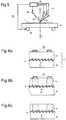
Bei einem zweiten Verfahren, das in den Fig. 6a, 6b und 6c dargestellt ist, wird zuerst ein Schichtverbund 2 aus wenigstens einer ersten Schicht 3 und einer Lackschicht 5 hergestellt. Falls die erste Schicht 3 eine stark reflektierende Schicht ist, dann ist die Schicht 3 mit Vorteil zwischen die Lackschicht 5 und eine weitere Schicht 8 eingebettet. Anschliessend wird der Fremdstoff als strukturierte Schicht 22 wiederum nach einem bekannten Verfahren aufgebracht (Fig. 6a). Bei einem nächsten Schritt wird der Schichtverbund 2 für eine vorbestimmte Zeitdauer einer erhöhten Temperatur ausgesetzt, die noch unterhalb des Erweichungspunktes der Lackschichten 3 und 5 liegt und beispielsweise 100° C beträgt, damit der Fremdstoff teilweise in die Schicht 5 hineindiffundiert (Fig. 6b). Die Zeitdauer ist vorzugsweise so lange gewählt, dass der Fremdstoff bis zu den Beugungsstrukturen 6 oder auch noch etwas weiter in die Schicht 3 hineindiffundiert. Es ist jedoch auch möglich, die gewünschte Information als Strukturen 7 zu schreiben, und optisch auszulesen, ohne dass der Fremdstoff bis zur Schicht 3 diffundiert. Bei Bedarf wird am Schluss die Schicht 22 wieder entfernt (Fig. 6c). Das maschinelle Lesen der Information erfolgt auch in diesem Fall von der Seite der Lackschicht 5.In a second method, which is shown in FIGS. 6a, 6b and 6c, a
Das zweite Verfahren eignet sich zur Individualisierung des Informationsträgers 1 mittels einer kleinen Einrichtung, die aus einem Schreibgerät zum Aufbringen der Schicht 22 auf den Schichtverbund 2, z.B. einem Tintenstrahldrucker oder einem Laserdrucker, und einem kleinen Heizgerät besteht. Dabei kann der Informationsträger 1 bereits vor der Individualisierung auf ein Dokument wie z.B. eine Identitätskarte oder ein Sicherheitspapier aufgebracht werden.The second method is suitable for individualizing the
Bei einem dritten Verfahren zur Herstellung eines derartigen Informationsträgers 1 wird ein Lack, der den Farbstoff als gelöste Teilchen enthält, nach einem bekannten Verfahren als unstrukturierte Schicht 5 auf die Schicht 3 bzw. 3a aufgebracht, in die vorgängig Beugungsstrukturen 6 z.B. durch Prägen, Abformen oder Abgiessen eingebracht wurden. Strukturen 7 werden erst bei der Individualisierung des Informationsträgers 1 gebildet, indem der Farbstoff durch lokales Erwärmen über eine dem Farbstoff eigene Grenztemperatur an der erwärmten Stelle eine lokal irreversible Umwandlung von einer transparenten Substanz in eine für das Licht zum Auslesen der Information absorbierende Substanz oder umgekehrt bewirkt. Die lokal veränderten Stellen und die unveränderten Stellen bilden zusammen die Strukturen 7. Beispielsweise ist die Lackschicht 5 vor dem Einschreiben der Information völlig transparent. Nach dem Einschreiben der Information ist die Lackschicht 5 an den lokal veränderten Stellen für das Licht zum Auslesen der Information undurchsichtig. Für das Lesegerät 15 wirkt die Veränderung der Transparenz gleich, wie wenn die Beugungsstruktur 6 in eine Mattstruktur umgewandelt wurde. Solche, ein thermochromes Verhalten aufweisende Farbstoffe sind z. B. aus den Schriften US-PS 2 663 654, US-PS 3 682 684 und EP 277 032 bekannt. Ein Vorteil dieses Verfahrens liegt darin, dass bei richtiger Dosierung der zugeführten Wärmeenergie die Oberfläche der Schichten 3, 5 unversehrt bleibt.In a third method for producing such an
Bestimmt die Differenz der Brechungindizes n3 und n5 der beiden Schichten 3 und 5 die optische Eigenschaft der Beugungsstruktur 6, dann ermöglicht ein Einbau des thermochromen Farbstoffs in der Lackschicht 5, oder in der Schicht 3, falls die Schicht 3 ebenfalls eine Lackschicht ist, beim Einschreiben den entsprechenden Brechungsindex einmal irreversibel zu ändern. Beim Auslesen der Information ist die Intensität der durch Beugungseffekte in den Photodetektor 17 gelenkten Lichtmenge davon abhängig, ob sich der Farbstoff an der lokalen Stelle durch Erwärmen umgewandelt hat und die Differenz der Brechungsindizes n3 und n5 lokal verändert ist.If the difference in the refractive indices n3 and n5 of the two
Das Lesegerät 15 kann die Information aus den Strukturen 7 auslesen, die als Muster der irreversibel veränderten Stellen auf dem Hintergrund der verbliebenen, unveränderten Schicht 3 bzw. 5 gebildet sind. Da das Lesegerät 15 zum Lesen der Information nur das an den Beugungsstrukturen 6 gebeugte Licht empfängt bzw. dessen Ferien feststellt, weisen diese Informationsträger den Vorteil auf, dass sie zwar einmal beschreibbar, jedoch nur mit grossem Aufwand nachzuahmen oder zu fälschen sind. Die Beugungsstrukturen 6 und die Unversehrtheit der Oberfläche ermöglichen auch dem Laien eine visuelle Überprüfung der Echtheit des Informationsträgers 1.The
Das lokale Erwärmen des Farbstoffes kann z.B. durch Bestrahlung mit intensivem Licht erfolgen. Mit Vorteil weist der Lichtstrahl eines Schreib-/Lesegerätes beim Einschreiben nicht nur eine höhere Intensität als das Licht zum Auslesen auf, sondern das Einschreiben erfolgt mit Licht, dessen Intensitätsmaximum in einem anderen Wellenlängenbereich liegt. Beispielsweise werden die Beugungsstrukturen 6 mit infrarotem Licht ausgelesen, während zum Einschreiben ein Lichtstrahl mit einer anderen, dem Farbstoff angepassten Wellenlänge eingesetzt wird.The dye can be heated locally, for example, by irradiation with intense light. Advantageously, the light beam of a read / write device not only has a higher intensity than the light for reading out when writing, but writing is done with light whose intensity maximum is in another wavelength range. For example, the
Ein Dokument, das mit einem Informationsträger versehen ist, der wenigstens aus den beiden Schichten 3 und 5 besteht, wobei eine der beiden Schichten 3, 5 mit einem Farbstoff dotiert ist, eignet sich besonders für Anwendungen, bei denen die Information dezentral eingeschrieben werden soll. Solche Anwendungen sind z.B. Ausweise aller Art oder auch eine optische Geldbörse, bei der der aktuelle Geldbetrag fortlaufend entlang einer Datenspur oder in einem zweidimensionalen Datenfeld eingeschrieben ist. Jeder Geldtransfer auf die Geldbörse oder von der Geldbörse wird von einem Schreib-/Lesegerät vorgenommen, wobei die Zahl der möglichen Transaktionen durch die Anzahl der optisch schreibbaren Bits vorgegeben ist.A document which is provided with an information carrier which consists at least of the two
Das in der Fig. 3 dargestellte Feld 10 kann anstelle oder zusätzlich zur Datenspur 12 ein zweidimensionales Datenfeld enthalten, wobei beim Auslesen mittels des Lesegerätes jeder beliebige xy-Datenpunkt des Datenfeldes adressierbar ist. Ein solches Datenfeld enthält wiederum erste und zweite Flächenelemente 13 bzw. 14. Die Flächenelemente 14, die zur Darstellung der maschinenlesbaren Information dienen, enthalten in der einfachsten Ausführung nur Beugungsstrukturen 6, die als Gitter mit vorbestimmtem Linienabstand, vorbestimmter Orientierung und vorbestimmter Profilform ausgebildet sind, damit sie das Licht des Leselichtstrahles in vorbestimmte Richtungen beugen. In einer weiteren Ausführung sind die zweiten Flächenelemente 14 in Unterelernente unterteilt. Die Unterelemente enthalten jeweils eine unterschiedliche Beugungsstruktur 6, die das Licht des Leselichtstrahles in unterschiedliche Richtungen beugt. Die Strukturierung der zweiten Schicht 4 zur Bildung der maschinenlesbaren Information kann dann so erfolgen, dass von beispielsweise zwei Unterelementen eines Flächenelementes 14 jeweils nur das eine mit der Schicht 4 bedeckt ist.The field 10 shown in FIG. 3 can contain a two-dimensional data field instead of or in addition to the
Zur Erzielung einer hohen Beugungseffizienz sind die Beugungsstrukturen 6 vorzugsweise als zweidimensionale Gitter ausgebildet, die durch einen konstanten Linienabstand und eine vorgegebene Profilform charakterisiert sind. Es ist jedoch auch möglich, einen Satz mit einer Anzahl von vorbestimmten Beugungsstrukturen 6 vorzusehen, die das Licht nicht in wenige ausgewählte Richtungen beugen, sondern die das Licht in vorbestimmte Raumwinkel beugen. In einem solchen Fall weist das dazugehörige Lesegerät anstelle einzelner Photodetektoren bevorzugt einen ein- oder zweidimensionalen Array an Photodetektoren auf, z.B. einen CCD-Sensor. Mit einem solchen CCD-Sensor ist die Intensitätsverteilung des in einen vorbestimmten Raumwinkel gebeugten Lichtes messbar.In order to achieve a high diffraction efficiency, the
Claims (15)
Translated fromGermanPriority Applications (7)
| Application Number | Priority Date | Filing Date | Title |
|---|---|---|---|
| DE59500254TDE59500254D1 (en) | 1995-03-16 | 1995-03-16 | Optical information carrier |
| EP95810177AEP0732667B1 (en) | 1995-03-16 | 1995-03-16 | Optical record carrier |
| AT95810177TATE153459T1 (en) | 1995-03-16 | 1995-03-16 | OPTICAL INFORMATION CARRIER |
| CA002171082ACA2171082C (en) | 1995-03-16 | 1996-03-05 | Optical information carrier |
| US08/613,860US5760961A (en) | 1995-03-16 | 1996-03-11 | Optical information carrier having diffractive features and diffraction modulation layers |
| JP8055609AJPH08286593A (en) | 1995-03-16 | 1996-03-13 | Optical information recording medium |
| AU48118/96AAU699421B2 (en) | 1995-03-16 | 1996-03-15 | Optical information carrier |
Applications Claiming Priority (1)
| Application Number | Priority Date | Filing Date | Title |
|---|---|---|---|
| EP95810177AEP0732667B1 (en) | 1995-03-16 | 1995-03-16 | Optical record carrier |
Publications (2)
| Publication Number | Publication Date |
|---|---|
| EP0732667A1true EP0732667A1 (en) | 1996-09-18 |
| EP0732667B1 EP0732667B1 (en) | 1997-05-21 |
Family
ID=8221715
Family Applications (1)
| Application Number | Title | Priority Date | Filing Date |
|---|---|---|---|
| EP95810177AExpired - LifetimeEP0732667B1 (en) | 1995-03-16 | 1995-03-16 | Optical record carrier |
Country Status (7)
| Country | Link |
|---|---|
| US (1) | US5760961A (en) |
| EP (1) | EP0732667B1 (en) |
| JP (1) | JPH08286593A (en) |
| AT (1) | ATE153459T1 (en) |
| AU (1) | AU699421B2 (en) |
| CA (1) | CA2171082C (en) |
| DE (1) | DE59500254D1 (en) |
Cited By (1)
| Publication number | Priority date | Publication date | Assignee | Title |
|---|---|---|---|---|
| EP1547807A3 (en)* | 2003-12-22 | 2007-02-07 | Giesecke & Devrient GmbH | Security element having a diffraction structure and method of manufacturing said element |
Families Citing this family (46)
| Publication number | Priority date | Publication date | Assignee | Title |
|---|---|---|---|---|
| US6005691A (en)* | 1996-12-11 | 1999-12-21 | Hewlett-Packard Company | High-security machine-readable holographic card |
| DE19721058A1 (en)* | 1997-05-20 | 1998-11-26 | Giesecke & Devrient Gmbh | Injection molded card with decorative layer |
| US6377970B1 (en) | 1998-03-31 | 2002-04-23 | Intel Corporation | Method and apparatus for computing a sum of packed data elements using SIMD multiply circuitry |
| US6243803B1 (en) | 1998-03-31 | 2001-06-05 | Intel Corporation | Method and apparatus for computing a packed absolute differences with plurality of sign bits using SIMD add circuitry |
| FI116086B (en)* | 2000-06-08 | 2005-09-15 | Avantone Oy | Check-marked paper or cardboard product and check-marked packaging |
| DE10036505A1 (en)* | 2000-07-27 | 2003-08-14 | Orga Kartensysteme Gmbh | Optically effective structure for personalizing cards and. Like., And methods for their production |
| JP4638022B2 (en)* | 2000-12-12 | 2011-02-23 | 株式会社トッパンTdkレーベル | Concealment seal and scratch media |
| DE10127980C1 (en)* | 2001-06-08 | 2003-01-16 | Ovd Kinegram Ag Zug | Diffractive security element |
| US6851608B1 (en)* | 2002-03-07 | 2005-02-08 | Commerciant, L.P. | System and method for uncontrolled velocity scanning |
| US7508608B2 (en) | 2004-11-17 | 2009-03-24 | Illumina, Inc. | Lithographically fabricated holographic optical identification element |
| JP4485949B2 (en)* | 2002-08-20 | 2010-06-23 | シヴェラ コーポレイション | Grating-based coded microparticles for multiplex experiments |
| US7164533B2 (en) | 2003-01-22 | 2007-01-16 | Cyvera Corporation | Hybrid random bead/chip based microarray |
| US7901630B2 (en) | 2002-08-20 | 2011-03-08 | Illumina, Inc. | Diffraction grating-based encoded microparticle assay stick |
| US7441703B2 (en) | 2002-08-20 | 2008-10-28 | Illumina, Inc. | Optical reader for diffraction grating-based encoded optical identification elements |
| US7872804B2 (en) | 2002-08-20 | 2011-01-18 | Illumina, Inc. | Encoded particle having a grating with variations in the refractive index |
| AU2003265583C1 (en)* | 2002-08-20 | 2009-05-21 | Cyvera Corporation | Diffraction grating-based optical identification element |
| US7900836B2 (en) | 2002-08-20 | 2011-03-08 | Illumina, Inc. | Optical reader system for substrates having an optically readable code |
| US7923260B2 (en) | 2002-08-20 | 2011-04-12 | Illumina, Inc. | Method of reading encoded particles |
| US7619819B2 (en) | 2002-08-20 | 2009-11-17 | Illumina, Inc. | Method and apparatus for drug product tracking using encoded optical identification elements |
| US7349158B2 (en)* | 2002-09-12 | 2008-03-25 | Cyvera Corporation | Diffraction grating-based encoded micro-particles for multiplexed experiments |
| US7092160B2 (en) | 2002-09-12 | 2006-08-15 | Illumina, Inc. | Method of manufacturing of diffraction grating-based optical identification element |
| EP1540590A1 (en)* | 2002-09-12 | 2005-06-15 | Cyvera Corporation | Assay stick comprising coded microbeads |
| US20100255603A9 (en) | 2002-09-12 | 2010-10-07 | Putnam Martin A | Method and apparatus for aligning microbeads in order to interrogate the same |
| WO2004025561A1 (en)* | 2002-09-12 | 2004-03-25 | Cyvera Corporation | Chemical synthesis using diffraction grating-based encoded optical elements |
| AU2003267192A1 (en) | 2002-09-12 | 2004-04-30 | Cyvera Corporation | Method and apparatus for aligning elongated microbeads in order to interrogate the same |
| EP1540592A1 (en)* | 2002-09-12 | 2005-06-15 | Cyvera Corporation | Method and apparatus for labeling using diffraction grating-based encoded optical identification elements |
| DE10328760B4 (en)* | 2003-06-25 | 2007-05-24 | Ovd Kinegram Ag | Optical security element |
| US7433123B2 (en) | 2004-02-19 | 2008-10-07 | Illumina, Inc. | Optical identification element having non-waveguide photosensitive substrate with diffraction grating therein |
| JP2006084944A (en)* | 2004-09-17 | 2006-03-30 | Sumitomo Electric Ind Ltd | Hologram sheet and manufacturing method thereof, hologram seal, hologram card and manufacturing method thereof |
| US20060082850A1 (en)* | 2004-10-18 | 2006-04-20 | Weaver Samuel P | Covert surface relief hologram design, fabrication and optical reconstruction for security applications |
| WO2006055735A2 (en) | 2004-11-16 | 2006-05-26 | Illumina, Inc | Scanner having spatial light modulator |
| ATE459933T1 (en) | 2004-11-16 | 2010-03-15 | Illumina Inc | METHOD AND APPARATUS FOR READING CODED MICROBALLS |
| US7604173B2 (en) | 2004-11-16 | 2009-10-20 | Illumina, Inc. | Holographically encoded elements for microarray and other tagging labeling applications, and method and apparatus for making and reading the same |
| FR2893424B1 (en)* | 2005-11-16 | 2008-01-25 | Arjowiggins Soc Par Actions Si | OPTICAL STRUCTURE, IN PARTICULAR FOR A DOCUMENT OF SECURITY AND / OR VALUE. |
| US7623624B2 (en) | 2005-11-22 | 2009-11-24 | Illumina, Inc. | Method and apparatus for labeling using optical identification elements characterized by X-ray diffraction |
| US7830575B2 (en) | 2006-04-10 | 2010-11-09 | Illumina, Inc. | Optical scanner with improved scan time |
| US8133638B2 (en)* | 2006-05-30 | 2012-03-13 | Brady Worldwide, Inc. | All-polymer grating microstructure |
| JP2008083599A (en)* | 2006-09-28 | 2008-04-10 | Toppan Printing Co Ltd | Optical element and display body using the same |
| ES2534234T3 (en)* | 2009-03-27 | 2015-04-20 | Hueck Folien Ges.M.B.H. | Security element, particularly security label with a tamper detection system |
| PL2267686T3 (en)* | 2009-05-07 | 2014-04-30 | Hueck Folien Gmbh | Safety label with authenticity and manipulation evidence |
| WO2013097028A1 (en)* | 2011-12-28 | 2013-07-04 | Canadian Bank Note Company, Limited | Improved method for printing an image onto a thermoplastic substrate, pre-forming plate used therefor and security instrument made therefrom |
| US9434205B2 (en) | 2014-09-12 | 2016-09-06 | Canadian Bank Note Company, Limited | Method for laminating a protective layer over a printed thermoplastic substrate and security document made therefrom |
| US10802321B2 (en)* | 2017-07-20 | 2020-10-13 | Benq Materials Corporation | Optical film for liquid crystal display |
| DE102019003947A1 (en)* | 2019-06-06 | 2020-12-10 | Giesecke+Devrient Currency Technology Gmbh | Method for producing an optically variable security element |
| DE102021001582A1 (en)* | 2021-03-25 | 2022-09-29 | Giesecke+Devrient Currency Technology Gmbh | Optically variable security element, manufacturing process and embossing arrangement |
| US12298529B2 (en)* | 2022-02-22 | 2025-05-13 | Northrop Grumman Systems Corporation | Spectrally-selective optical element |
Citations (7)
| Publication number | Priority date | Publication date | Assignee | Title |
|---|---|---|---|---|
| US3703407A (en)* | 1970-12-15 | 1972-11-21 | Rca Corp | Relief phase holograms |
| DE3233197A1 (en)* | 1981-10-27 | 1983-05-05 | LGZ Landis & Gyr Zug AG, 6301 Zug | DOCUMENT WITH A SECURITY CHARACTERISTIC AND METHOD FOR CHECKING THE DOCUMENT FOR AUTHENTICITY |
| EP0201323A2 (en)* | 1985-05-07 | 1986-11-12 | Dai Nippon Insatsu Kabushiki Kaisha | Article incorporating a transparent hologramm |
| EP0264277A2 (en)* | 1986-10-15 | 1988-04-20 | Kyodo Printing Co., Ltd. | Optical recording card having hologram contained therein and method of producing the same |
| WO1991006925A1 (en)* | 1989-10-26 | 1991-05-16 | Amblehurst Limited | Optical device |
| EP0570120A2 (en)* | 1992-04-23 | 1993-11-18 | Flexcon Company Inc. | Optical authentication device |
| WO1994025288A1 (en)* | 1993-04-24 | 1994-11-10 | Leonhard Kurz Gmbh & Co. | Decorative covering structure and its use |
Family Cites Families (9)
| Publication number | Priority date | Publication date | Assignee | Title |
|---|---|---|---|---|
| US4576439A (en)* | 1982-09-15 | 1986-03-18 | Rca Corporation | Reflective diffractive authenticating device |
| US4921319A (en)* | 1989-01-23 | 1990-05-01 | American Bank Note Holographics, Inc. | Surface relief hologram structure with reflection from an air interface |
| US5522623A (en)* | 1990-03-29 | 1996-06-04 | Technical Systems Corp. | Coded identification card and other standardized documents |
| GB9019784D0 (en)* | 1990-09-10 | 1990-10-24 | Amblehurst Ltd | Security device |
| DE4033300C2 (en)* | 1990-10-19 | 1994-06-23 | Gao Ges Automation Org | Multi-layer, card-shaped data carrier and method for producing the same |
| US5379131A (en)* | 1991-12-11 | 1995-01-03 | Dai Nippon Printing Co., Ltd. | Method of preventing forgery of diffraction grating pattern and forgery-proof diffraction grating pattern recording structure |
| US5432329A (en)* | 1992-02-07 | 1995-07-11 | American Bank Note Holographics | Automated holographic optical recognition and decoding system for verification |
| US5549774A (en)* | 1992-05-11 | 1996-08-27 | Avery Dennison Corporation | Method of enhancing the visibility of diffraction pattern surface embossment |
| JPH06110382A (en)* | 1992-09-30 | 1994-04-22 | Dainippon Printing Co Ltd | Hologram, correctness confirmation method and confirmation device using the hologram |
- 1995
- 1995-03-16DEDE59500254Tpatent/DE59500254D1/ennot_activeExpired - Lifetime
- 1995-03-16ATAT95810177Tpatent/ATE153459T1/ennot_activeIP Right Cessation
- 1995-03-16EPEP95810177Apatent/EP0732667B1/ennot_activeExpired - Lifetime
- 1996
- 1996-03-05CACA002171082Apatent/CA2171082C/ennot_activeExpired - Fee Related
- 1996-03-11USUS08/613,860patent/US5760961A/ennot_activeExpired - Fee Related
- 1996-03-13JPJP8055609Apatent/JPH08286593A/enactivePending
- 1996-03-15AUAU48118/96Apatent/AU699421B2/ennot_activeCeased
Patent Citations (7)
| Publication number | Priority date | Publication date | Assignee | Title |
|---|---|---|---|---|
| US3703407A (en)* | 1970-12-15 | 1972-11-21 | Rca Corp | Relief phase holograms |
| DE3233197A1 (en)* | 1981-10-27 | 1983-05-05 | LGZ Landis & Gyr Zug AG, 6301 Zug | DOCUMENT WITH A SECURITY CHARACTERISTIC AND METHOD FOR CHECKING THE DOCUMENT FOR AUTHENTICITY |
| EP0201323A2 (en)* | 1985-05-07 | 1986-11-12 | Dai Nippon Insatsu Kabushiki Kaisha | Article incorporating a transparent hologramm |
| EP0264277A2 (en)* | 1986-10-15 | 1988-04-20 | Kyodo Printing Co., Ltd. | Optical recording card having hologram contained therein and method of producing the same |
| WO1991006925A1 (en)* | 1989-10-26 | 1991-05-16 | Amblehurst Limited | Optical device |
| EP0570120A2 (en)* | 1992-04-23 | 1993-11-18 | Flexcon Company Inc. | Optical authentication device |
| WO1994025288A1 (en)* | 1993-04-24 | 1994-11-10 | Leonhard Kurz Gmbh & Co. | Decorative covering structure and its use |
Cited By (1)
| Publication number | Priority date | Publication date | Assignee | Title |
|---|---|---|---|---|
| EP1547807A3 (en)* | 2003-12-22 | 2007-02-07 | Giesecke & Devrient GmbH | Security element having a diffraction structure and method of manufacturing said element |
Also Published As
| Publication number | Publication date |
|---|---|
| JPH08286593A (en) | 1996-11-01 |
| AU4811896A (en) | 1996-09-26 |
| CA2171082C (en) | 2006-11-07 |
| DE59500254D1 (en) | 1997-06-26 |
| ATE153459T1 (en) | 1997-06-15 |
| EP0732667B1 (en) | 1997-05-21 |
| AU699421B2 (en) | 1998-12-03 |
| US5760961A (en) | 1998-06-02 |
| CA2171082A1 (en) | 1996-09-17 |
Similar Documents
| Publication | Publication Date | Title |
|---|---|---|
| EP0732667B1 (en) | Optical record carrier | |
| DE69620636T2 (en) | OPTICAL INFORMATION CARRIER | |
| AT392439B (en) | ID CARD AND METHOD FOR THE PRODUCTION THEREOF | |
| EP0741370B1 (en) | Method for applying a security element on a substrate | |
| EP1697146B1 (en) | Data support with identifications written thereon by means of a laser beam and method for production thereof | |
| EP1716545B1 (en) | Object of value comprising a moire pattern | |
| EP3112948B1 (en) | Method and device for verifying holograms with watermark-like structure | |
| EP1972463B1 (en) | Security element | |
| DE2555214A1 (en) | DOCUMENT | |
| DE102006006323B4 (en) | Multi-layer body with an optically machine-readable identifier | |
| DE19924750A1 (en) | Reading arrangement for information strips with optically coded information | |
| DE102006023084A1 (en) | Value document with security element | |
| EP0718795B1 (en) | Optically machine readable data carrier | |
| CH691750A5 (en) | Optical information carrier made of composite laminate with carrier foil | |
| EP1718475B1 (en) | Security element comprising a lens grid and method for the production thereof | |
| DE102007044486B4 (en) | Security element to increase the security against forgery of a security document and security document | |
| EP2215529B1 (en) | Method and device for producing holograms having an individually exposed watermark-type structure | |
| EP3406458A1 (en) | Security element with reflective surface area | |
| AT404696B (en) | Information medium with heat-sensitive lattice structures | |
| EP2167317B1 (en) | Printing device | |
| EP2214914B1 (en) | Method for producing a security feature for a document and corresponding document | |
| DE102007063504A1 (en) | Individualized hologram manufacturing method for e.g. passport, involves impressing modulated coherent light at weakly and strongly scattered regions of master so that background pattern is detectable by individualization information | |
| DE60120737T2 (en) | IRISING MATERIALS AND DEVICES | |
| CH690529A5 (en) | Optical information carrier made of composite laminate with carrier foil | |
| EP3429867B1 (en) | Card-type data carrier |
Legal Events
| Date | Code | Title | Description |
|---|---|---|---|
| GRAG | Despatch of communication of intention to grant | Free format text:ORIGINAL CODE: EPIDOS AGRA | |
| PUAI | Public reference made under article 153(3) epc to a published international application that has entered the european phase | Free format text:ORIGINAL CODE: 0009012 | |
| 17P | Request for examination filed | Effective date:19951011 | |
| AK | Designated contracting states | Kind code of ref document:A1 Designated state(s):AT CH DE FR GB LI NL | |
| AX | Request for extension of the european patent | Free format text:LT;SI | |
| RAX | Requested extension states of the european patent have changed | Free format text:LT;SI | |
| GRAH | Despatch of communication of intention to grant a patent | Free format text:ORIGINAL CODE: EPIDOS IGRA | |
| GRAH | Despatch of communication of intention to grant a patent | Free format text:ORIGINAL CODE: EPIDOS IGRA | |
| GRAA | (expected) grant | Free format text:ORIGINAL CODE: 0009210 | |
| AK | Designated contracting states | Kind code of ref document:B1 Designated state(s):AT CH DE FR GB LI NL | |
| AX | Request for extension of the european patent | Free format text:LT;SI | |
| REF | Corresponds to: | Ref document number:153459 Country of ref document:AT Date of ref document:19970615 Kind code of ref document:T | |
| REG | Reference to a national code | Ref country code:CH Ref legal event code:EP | |
| GBT | Gb: translation of ep patent filed (gb section 77(6)(a)/1977) | Effective date:19970522 | |
| REF | Corresponds to: | Ref document number:59500254 Country of ref document:DE Date of ref document:19970626 | |
| ET | Fr: translation filed | ||
| PLBE | No opposition filed within time limit | Free format text:ORIGINAL CODE: 0009261 | |
| STAA | Information on the status of an ep patent application or granted ep patent | Free format text:STATUS: NO OPPOSITION FILED WITHIN TIME LIMIT | |
| 26N | No opposition filed | ||
| REG | Reference to a national code | Ref country code:CH Ref legal event code:PUE Owner name:ELECTROWATT TECHNOLOGY INNOVATION AG TRANSFER- OVD Ref country code:CH Ref legal event code:PFA Free format text:LANDIS & GYR TECHNOLOGY INNOVATION AG TRANSFER- ELECTROWATT TECHNOLOGY INNOVATION AG Ref country code:CH Ref legal event code:NV Representative=s name:ELECTROWATT TECHNOLOGY INNOVATION AG C-IPR, 4470 | |
| NLS | Nl: assignments of ep-patents | Owner name:OVD KINEGRAM AG | |
| NLT1 | Nl: modifications of names registered in virtue of documents presented to the patent office pursuant to art. 16 a, paragraph 1 | Owner name:ELECTROWATT TECHNOLOGY INNOVATION AG | |
| REG | Reference to a national code | Ref country code:FR Ref legal event code:TP | |
| REG | Reference to a national code | Ref country code:CH Ref legal event code:NV Representative=s name:PATENTANWALTSBUERO DR. URS FALK | |
| REG | Reference to a national code | Ref country code:GB Ref legal event code:732E | |
| REG | Reference to a national code | Ref country code:GB Ref legal event code:IF02 | |
| PGFP | Annual fee paid to national office [announced via postgrant information from national office to epo] | Ref country code:NL Payment date:20060320 Year of fee payment:12 | |
| PGFP | Annual fee paid to national office [announced via postgrant information from national office to epo] | Ref country code:GB Payment date:20060323 Year of fee payment:12 | |
| PGFP | Annual fee paid to national office [announced via postgrant information from national office to epo] | Ref country code:AT Payment date:20060324 Year of fee payment:12 | |
| PG25 | Lapsed in a contracting state [announced via postgrant information from national office to epo] | Ref country code:AT Free format text:LAPSE BECAUSE OF NON-PAYMENT OF DUE FEES Effective date:20070316 | |
| GBPC | Gb: european patent ceased through non-payment of renewal fee | Effective date:20070316 | |
| NLV4 | Nl: lapsed or anulled due to non-payment of the annual fee | Effective date:20071001 | |
| PG25 | Lapsed in a contracting state [announced via postgrant information from national office to epo] | Ref country code:NL Free format text:LAPSE BECAUSE OF NON-PAYMENT OF DUE FEES Effective date:20071001 | |
| PG25 | Lapsed in a contracting state [announced via postgrant information from national office to epo] | Ref country code:GB Free format text:LAPSE BECAUSE OF NON-PAYMENT OF DUE FEES Effective date:20070316 | |
| PGFP | Annual fee paid to national office [announced via postgrant information from national office to epo] | Ref country code:FR Payment date:20070321 Year of fee payment:13 | |
| REG | Reference to a national code | Ref country code:FR Ref legal event code:ST Effective date:20081125 | |
| PG25 | Lapsed in a contracting state [announced via postgrant information from national office to epo] | Ref country code:FR Free format text:LAPSE BECAUSE OF NON-PAYMENT OF DUE FEES Effective date:20080331 | |
| PGFP | Annual fee paid to national office [announced via postgrant information from national office to epo] | Ref country code:DE Payment date:20130320 Year of fee payment:19 Ref country code:CH Payment date:20130319 Year of fee payment:19 | |
| REG | Reference to a national code | Ref country code:DE Ref legal event code:R119 Ref document number:59500254 Country of ref document:DE | |
| REG | Reference to a national code | Ref country code:CH Ref legal event code:PL | |
| REG | Reference to a national code | Ref country code:DE Ref legal event code:R119 Ref document number:59500254 Country of ref document:DE Effective date:20141001 | |
| PG25 | Lapsed in a contracting state [announced via postgrant information from national office to epo] | Ref country code:CH Free format text:LAPSE BECAUSE OF NON-PAYMENT OF DUE FEES Effective date:20140331 Ref country code:LI Free format text:LAPSE BECAUSE OF NON-PAYMENT OF DUE FEES Effective date:20140331 Ref country code:DE Free format text:LAPSE BECAUSE OF NON-PAYMENT OF DUE FEES Effective date:20141001 |