EP0724776B1 - Method for stitch bonding of wires to integrated circuit bonding pads - Google Patents
Method for stitch bonding of wires to integrated circuit bonding padsDownload PDFInfo
- Publication number
- EP0724776B1 EP0724776B1EP95930924AEP95930924AEP0724776B1EP 0724776 B1EP0724776 B1EP 0724776B1EP 95930924 AEP95930924 AEP 95930924AEP 95930924 AEP95930924 AEP 95930924AEP 0724776 B1EP0724776 B1EP 0724776B1
- Authority
- EP
- European Patent Office
- Prior art keywords
- capillary
- bonding
- bonding pad
- integrated circuit
- wire
- Prior art date
- Legal status (The legal status is an assumption and is not a legal conclusion. Google has not performed a legal analysis and makes no representation as to the accuracy of the status listed.)
- Expired - Lifetime
Links
- 238000000034methodMethods0.000titleclaimsabstractdescription26
- 238000003466weldingMethods0.000claimsdescription10
- 238000002161passivationMethods0.000abstractdescription16
- 238000007796conventional methodMethods0.000description5
- 230000007797corrosionEffects0.000description5
- 238000005260corrosionMethods0.000description5
- 239000000463materialSubstances0.000description4
- 239000000758substrateSubstances0.000description4
- XAGFODPZIPBFFR-UHFFFAOYSA-NaluminiumChemical compound[Al]XAGFODPZIPBFFR-UHFFFAOYSA-N0.000description2
- 229910052782aluminiumInorganic materials0.000description2
- PCHJSUWPFVWCPO-UHFFFAOYSA-NgoldChemical compound[Au]PCHJSUWPFVWCPO-UHFFFAOYSA-N0.000description2
- 229910052737goldInorganic materials0.000description2
- 239000010931goldSubstances0.000description2
- 238000004519manufacturing processMethods0.000description2
- RYGMFSIKBFXOCR-UHFFFAOYSA-NCopperChemical compound[Cu]RYGMFSIKBFXOCR-UHFFFAOYSA-N0.000description1
- 230000015572biosynthetic processEffects0.000description1
- 239000011248coating agentSubstances0.000description1
- 238000000576coating methodMethods0.000description1
- 230000006835compressionEffects0.000description1
- 238000007906compressionMethods0.000description1
- 238000010276constructionMethods0.000description1
- 229910052802copperInorganic materials0.000description1
- 239000010949copperSubstances0.000description1
- 238000005336crackingMethods0.000description1
- 230000000694effectsEffects0.000description1
- 238000004806packaging method and processMethods0.000description1
- 230000001681protective effectEffects0.000description1
- 239000004065semiconductorSubstances0.000description1
- 150000003377silicon compoundsChemical class0.000description1
- 238000013519translationMethods0.000description1
- 230000014616translationEffects0.000description1
Images


Classifications
- H—ELECTRICITY
- H01—ELECTRIC ELEMENTS
- H01L—SEMICONDUCTOR DEVICES NOT COVERED BY CLASS H10
- H01L24/00—Arrangements for connecting or disconnecting semiconductor or solid-state bodies; Methods or apparatus related thereto
- H01L24/80—Methods for connecting semiconductor or other solid state bodies using means for bonding being attached to, or being formed on, the surface to be connected
- H01L24/85—Methods for connecting semiconductor or other solid state bodies using means for bonding being attached to, or being formed on, the surface to be connected using a wire connector
- B—PERFORMING OPERATIONS; TRANSPORTING
- B23—MACHINE TOOLS; METAL-WORKING NOT OTHERWISE PROVIDED FOR
- B23K—SOLDERING OR UNSOLDERING; WELDING; CLADDING OR PLATING BY SOLDERING OR WELDING; CUTTING BY APPLYING HEAT LOCALLY, e.g. FLAME CUTTING; WORKING BY LASER BEAM
- B23K20/00—Non-electric welding by applying impact or other pressure, with or without the application of heat, e.g. cladding or plating
- B23K20/002—Non-electric welding by applying impact or other pressure, with or without the application of heat, e.g. cladding or plating specially adapted for particular articles or work
- B23K20/004—Wire welding
- B23K20/005—Capillary welding
- H—ELECTRICITY
- H01—ELECTRIC ELEMENTS
- H01L—SEMICONDUCTOR DEVICES NOT COVERED BY CLASS H10
- H01L21/00—Processes or apparatus adapted for the manufacture or treatment of semiconductor or solid state devices or of parts thereof
- H01L21/02—Manufacture or treatment of semiconductor devices or of parts thereof
- H01L21/04—Manufacture or treatment of semiconductor devices or of parts thereof the devices having potential barriers, e.g. a PN junction, depletion layer or carrier concentration layer
- H01L21/50—Assembly of semiconductor devices using processes or apparatus not provided for in a single one of the groups H01L21/18 - H01L21/326 or H10D48/04 - H10D48/07 e.g. sealing of a cap to a base of a container
- H01L21/60—Attaching or detaching leads or other conductive members, to be used for carrying current to or from the device in operation
- H01L21/607—Attaching or detaching leads or other conductive members, to be used for carrying current to or from the device in operation involving the application of mechanical vibrations, e.g. ultrasonic vibrations
- H—ELECTRICITY
- H01—ELECTRIC ELEMENTS
- H01L—SEMICONDUCTOR DEVICES NOT COVERED BY CLASS H10
- H01L24/00—Arrangements for connecting or disconnecting semiconductor or solid-state bodies; Methods or apparatus related thereto
- H01L24/01—Means for bonding being attached to, or being formed on, the surface to be connected, e.g. chip-to-package, die-attach, "first-level" interconnects; Manufacturing methods related thereto
- H01L24/02—Bonding areas ; Manufacturing methods related thereto
- H01L24/03—Manufacturing methods
- H—ELECTRICITY
- H01—ELECTRIC ELEMENTS
- H01L—SEMICONDUCTOR DEVICES NOT COVERED BY CLASS H10
- H01L24/00—Arrangements for connecting or disconnecting semiconductor or solid-state bodies; Methods or apparatus related thereto
- H01L24/01—Means for bonding being attached to, or being formed on, the surface to be connected, e.g. chip-to-package, die-attach, "first-level" interconnects; Manufacturing methods related thereto
- H01L24/02—Bonding areas ; Manufacturing methods related thereto
- H01L24/04—Structure, shape, material or disposition of the bonding areas prior to the connecting process
- H01L24/05—Structure, shape, material or disposition of the bonding areas prior to the connecting process of an individual bonding area
- H—ELECTRICITY
- H01—ELECTRIC ELEMENTS
- H01L—SEMICONDUCTOR DEVICES NOT COVERED BY CLASS H10
- H01L24/00—Arrangements for connecting or disconnecting semiconductor or solid-state bodies; Methods or apparatus related thereto
- H01L24/01—Means for bonding being attached to, or being formed on, the surface to be connected, e.g. chip-to-package, die-attach, "first-level" interconnects; Manufacturing methods related thereto
- H01L24/42—Wire connectors; Manufacturing methods related thereto
- H01L24/47—Structure, shape, material or disposition of the wire connectors after the connecting process
- H01L24/48—Structure, shape, material or disposition of the wire connectors after the connecting process of an individual wire connector
- H—ELECTRICITY
- H01—ELECTRIC ELEMENTS
- H01L—SEMICONDUCTOR DEVICES NOT COVERED BY CLASS H10
- H01L24/00—Arrangements for connecting or disconnecting semiconductor or solid-state bodies; Methods or apparatus related thereto
- H01L24/74—Apparatus for manufacturing arrangements for connecting or disconnecting semiconductor or solid-state bodies
- H01L24/78—Apparatus for connecting with wire connectors
- H—ELECTRICITY
- H01—ELECTRIC ELEMENTS
- H01L—SEMICONDUCTOR DEVICES NOT COVERED BY CLASS H10
- H01L2224/00—Indexing scheme for arrangements for connecting or disconnecting semiconductor or solid-state bodies and methods related thereto as covered by H01L24/00
- H01L2224/01—Means for bonding being attached to, or being formed on, the surface to be connected, e.g. chip-to-package, die-attach, "first-level" interconnects; Manufacturing methods related thereto
- H01L2224/02—Bonding areas; Manufacturing methods related thereto
- H01L2224/0212—Auxiliary members for bonding areas, e.g. spacers
- H01L2224/02122—Auxiliary members for bonding areas, e.g. spacers being formed on the semiconductor or solid-state body
- H01L2224/02163—Auxiliary members for bonding areas, e.g. spacers being formed on the semiconductor or solid-state body on the bonding area
- H01L2224/02165—Reinforcing structures
- H01L2224/02166—Collar structures
- H—ELECTRICITY
- H01—ELECTRIC ELEMENTS
- H01L—SEMICONDUCTOR DEVICES NOT COVERED BY CLASS H10
- H01L2224/00—Indexing scheme for arrangements for connecting or disconnecting semiconductor or solid-state bodies and methods related thereto as covered by H01L24/00
- H01L2224/01—Means for bonding being attached to, or being formed on, the surface to be connected, e.g. chip-to-package, die-attach, "first-level" interconnects; Manufacturing methods related thereto
- H01L2224/02—Bonding areas; Manufacturing methods related thereto
- H01L2224/04—Structure, shape, material or disposition of the bonding areas prior to the connecting process
- H01L2224/04042—Bonding areas specifically adapted for wire connectors, e.g. wirebond pads
- H—ELECTRICITY
- H01—ELECTRIC ELEMENTS
- H01L—SEMICONDUCTOR DEVICES NOT COVERED BY CLASS H10
- H01L2224/00—Indexing scheme for arrangements for connecting or disconnecting semiconductor or solid-state bodies and methods related thereto as covered by H01L24/00
- H01L2224/01—Means for bonding being attached to, or being formed on, the surface to be connected, e.g. chip-to-package, die-attach, "first-level" interconnects; Manufacturing methods related thereto
- H01L2224/02—Bonding areas; Manufacturing methods related thereto
- H01L2224/04—Structure, shape, material or disposition of the bonding areas prior to the connecting process
- H01L2224/05—Structure, shape, material or disposition of the bonding areas prior to the connecting process of an individual bonding area
- H01L2224/05001—Internal layers
- H01L2224/05073—Single internal layer
- H—ELECTRICITY
- H01—ELECTRIC ELEMENTS
- H01L—SEMICONDUCTOR DEVICES NOT COVERED BY CLASS H10
- H01L2224/00—Indexing scheme for arrangements for connecting or disconnecting semiconductor or solid-state bodies and methods related thereto as covered by H01L24/00
- H01L2224/01—Means for bonding being attached to, or being formed on, the surface to be connected, e.g. chip-to-package, die-attach, "first-level" interconnects; Manufacturing methods related thereto
- H01L2224/02—Bonding areas; Manufacturing methods related thereto
- H01L2224/04—Structure, shape, material or disposition of the bonding areas prior to the connecting process
- H01L2224/05—Structure, shape, material or disposition of the bonding areas prior to the connecting process of an individual bonding area
- H01L2224/0554—External layer
- H01L2224/05599—Material
- H01L2224/056—Material with a principal constituent of the material being a metal or a metalloid, e.g. boron [B], silicon [Si], germanium [Ge], arsenic [As], antimony [Sb], tellurium [Te] and polonium [Po], and alloys thereof
- H01L2224/05617—Material with a principal constituent of the material being a metal or a metalloid, e.g. boron [B], silicon [Si], germanium [Ge], arsenic [As], antimony [Sb], tellurium [Te] and polonium [Po], and alloys thereof the principal constituent melting at a temperature of greater than or equal to 400°C and less than 950°C
- H01L2224/05624—Aluminium [Al] as principal constituent
- H—ELECTRICITY
- H01—ELECTRIC ELEMENTS
- H01L—SEMICONDUCTOR DEVICES NOT COVERED BY CLASS H10
- H01L2224/00—Indexing scheme for arrangements for connecting or disconnecting semiconductor or solid-state bodies and methods related thereto as covered by H01L24/00
- H01L2224/01—Means for bonding being attached to, or being formed on, the surface to be connected, e.g. chip-to-package, die-attach, "first-level" interconnects; Manufacturing methods related thereto
- H01L2224/42—Wire connectors; Manufacturing methods related thereto
- H01L2224/44—Structure, shape, material or disposition of the wire connectors prior to the connecting process
- H01L2224/45—Structure, shape, material or disposition of the wire connectors prior to the connecting process of an individual wire connector
- H01L2224/45001—Core members of the connector
- H01L2224/45099—Material
- H01L2224/451—Material with a principal constituent of the material being a metal or a metalloid, e.g. boron (B), silicon (Si), germanium (Ge), arsenic (As), antimony (Sb), tellurium (Te) and polonium (Po), and alloys thereof
- H01L2224/45117—Material with a principal constituent of the material being a metal or a metalloid, e.g. boron (B), silicon (Si), germanium (Ge), arsenic (As), antimony (Sb), tellurium (Te) and polonium (Po), and alloys thereof the principal constituent melting at a temperature of greater than or equal to 400°C and less than 950°C
- H01L2224/45124—Aluminium (Al) as principal constituent
- H—ELECTRICITY
- H01—ELECTRIC ELEMENTS
- H01L—SEMICONDUCTOR DEVICES NOT COVERED BY CLASS H10
- H01L2224/00—Indexing scheme for arrangements for connecting or disconnecting semiconductor or solid-state bodies and methods related thereto as covered by H01L24/00
- H01L2224/01—Means for bonding being attached to, or being formed on, the surface to be connected, e.g. chip-to-package, die-attach, "first-level" interconnects; Manufacturing methods related thereto
- H01L2224/42—Wire connectors; Manufacturing methods related thereto
- H01L2224/44—Structure, shape, material or disposition of the wire connectors prior to the connecting process
- H01L2224/45—Structure, shape, material or disposition of the wire connectors prior to the connecting process of an individual wire connector
- H01L2224/45001—Core members of the connector
- H01L2224/45099—Material
- H01L2224/451—Material with a principal constituent of the material being a metal or a metalloid, e.g. boron (B), silicon (Si), germanium (Ge), arsenic (As), antimony (Sb), tellurium (Te) and polonium (Po), and alloys thereof
- H01L2224/45138—Material with a principal constituent of the material being a metal or a metalloid, e.g. boron (B), silicon (Si), germanium (Ge), arsenic (As), antimony (Sb), tellurium (Te) and polonium (Po), and alloys thereof the principal constituent melting at a temperature of greater than or equal to 950°C and less than 1550°C
- H01L2224/45144—Gold (Au) as principal constituent
- H—ELECTRICITY
- H01—ELECTRIC ELEMENTS
- H01L—SEMICONDUCTOR DEVICES NOT COVERED BY CLASS H10
- H01L2224/00—Indexing scheme for arrangements for connecting or disconnecting semiconductor or solid-state bodies and methods related thereto as covered by H01L24/00
- H01L2224/01—Means for bonding being attached to, or being formed on, the surface to be connected, e.g. chip-to-package, die-attach, "first-level" interconnects; Manufacturing methods related thereto
- H01L2224/42—Wire connectors; Manufacturing methods related thereto
- H01L2224/44—Structure, shape, material or disposition of the wire connectors prior to the connecting process
- H01L2224/45—Structure, shape, material or disposition of the wire connectors prior to the connecting process of an individual wire connector
- H01L2224/45001—Core members of the connector
- H01L2224/45099—Material
- H01L2224/451—Material with a principal constituent of the material being a metal or a metalloid, e.g. boron (B), silicon (Si), germanium (Ge), arsenic (As), antimony (Sb), tellurium (Te) and polonium (Po), and alloys thereof
- H01L2224/45138—Material with a principal constituent of the material being a metal or a metalloid, e.g. boron (B), silicon (Si), germanium (Ge), arsenic (As), antimony (Sb), tellurium (Te) and polonium (Po), and alloys thereof the principal constituent melting at a temperature of greater than or equal to 950°C and less than 1550°C
- H01L2224/45147—Copper (Cu) as principal constituent
- H—ELECTRICITY
- H01—ELECTRIC ELEMENTS
- H01L—SEMICONDUCTOR DEVICES NOT COVERED BY CLASS H10
- H01L2224/00—Indexing scheme for arrangements for connecting or disconnecting semiconductor or solid-state bodies and methods related thereto as covered by H01L24/00
- H01L2224/01—Means for bonding being attached to, or being formed on, the surface to be connected, e.g. chip-to-package, die-attach, "first-level" interconnects; Manufacturing methods related thereto
- H01L2224/42—Wire connectors; Manufacturing methods related thereto
- H01L2224/47—Structure, shape, material or disposition of the wire connectors after the connecting process
- H01L2224/48—Structure, shape, material or disposition of the wire connectors after the connecting process of an individual wire connector
- H01L2224/4805—Shape
- H01L2224/4809—Loop shape
- H01L2224/48091—Arched
- H—ELECTRICITY
- H01—ELECTRIC ELEMENTS
- H01L—SEMICONDUCTOR DEVICES NOT COVERED BY CLASS H10
- H01L2224/00—Indexing scheme for arrangements for connecting or disconnecting semiconductor or solid-state bodies and methods related thereto as covered by H01L24/00
- H01L2224/01—Means for bonding being attached to, or being formed on, the surface to be connected, e.g. chip-to-package, die-attach, "first-level" interconnects; Manufacturing methods related thereto
- H01L2224/42—Wire connectors; Manufacturing methods related thereto
- H01L2224/47—Structure, shape, material or disposition of the wire connectors after the connecting process
- H01L2224/48—Structure, shape, material or disposition of the wire connectors after the connecting process of an individual wire connector
- H01L2224/481—Disposition
- H01L2224/48135—Connecting between different semiconductor or solid-state bodies, i.e. chip-to-chip
- H01L2224/48137—Connecting between different semiconductor or solid-state bodies, i.e. chip-to-chip the bodies being arranged next to each other, e.g. on a common substrate
- H—ELECTRICITY
- H01—ELECTRIC ELEMENTS
- H01L—SEMICONDUCTOR DEVICES NOT COVERED BY CLASS H10
- H01L2224/00—Indexing scheme for arrangements for connecting or disconnecting semiconductor or solid-state bodies and methods related thereto as covered by H01L24/00
- H01L2224/01—Means for bonding being attached to, or being formed on, the surface to be connected, e.g. chip-to-package, die-attach, "first-level" interconnects; Manufacturing methods related thereto
- H01L2224/42—Wire connectors; Manufacturing methods related thereto
- H01L2224/47—Structure, shape, material or disposition of the wire connectors after the connecting process
- H01L2224/48—Structure, shape, material or disposition of the wire connectors after the connecting process of an individual wire connector
- H01L2224/484—Connecting portions
- H01L2224/48463—Connecting portions the connecting portion on the bonding area of the semiconductor or solid-state body being a ball bond
- H01L2224/48465—Connecting portions the connecting portion on the bonding area of the semiconductor or solid-state body being a ball bond the other connecting portion not on the bonding area being a wedge bond, i.e. ball-to-wedge, regular stitch
- H—ELECTRICITY
- H01—ELECTRIC ELEMENTS
- H01L—SEMICONDUCTOR DEVICES NOT COVERED BY CLASS H10
- H01L2224/00—Indexing scheme for arrangements for connecting or disconnecting semiconductor or solid-state bodies and methods related thereto as covered by H01L24/00
- H01L2224/01—Means for bonding being attached to, or being formed on, the surface to be connected, e.g. chip-to-package, die-attach, "first-level" interconnects; Manufacturing methods related thereto
- H01L2224/42—Wire connectors; Manufacturing methods related thereto
- H01L2224/47—Structure, shape, material or disposition of the wire connectors after the connecting process
- H01L2224/48—Structure, shape, material or disposition of the wire connectors after the connecting process of an individual wire connector
- H01L2224/484—Connecting portions
- H01L2224/4847—Connecting portions the connecting portion on the bonding area of the semiconductor or solid-state body being a wedge bond
- H01L2224/48471—Connecting portions the connecting portion on the bonding area of the semiconductor or solid-state body being a wedge bond the other connecting portion not on the bonding area being a ball bond, i.e. wedge-to-ball, reverse stitch
- H—ELECTRICITY
- H01—ELECTRIC ELEMENTS
- H01L—SEMICONDUCTOR DEVICES NOT COVERED BY CLASS H10
- H01L2224/00—Indexing scheme for arrangements for connecting or disconnecting semiconductor or solid-state bodies and methods related thereto as covered by H01L24/00
- H01L2224/01—Means for bonding being attached to, or being formed on, the surface to be connected, e.g. chip-to-package, die-attach, "first-level" interconnects; Manufacturing methods related thereto
- H01L2224/42—Wire connectors; Manufacturing methods related thereto
- H01L2224/47—Structure, shape, material or disposition of the wire connectors after the connecting process
- H01L2224/48—Structure, shape, material or disposition of the wire connectors after the connecting process of an individual wire connector
- H01L2224/485—Material
- H01L2224/48505—Material at the bonding interface
- H01L2224/48599—Principal constituent of the connecting portion of the wire connector being Gold (Au)
- H01L2224/486—Principal constituent of the connecting portion of the wire connector being Gold (Au) with a principal constituent of the bonding area being a metal or a metalloid, e.g. boron (B), silicon (Si), germanium (Ge), arsenic (As), antimony (Sb), tellurium (Te) and polonium (Po), and alloys thereof
- H01L2224/48617—Principal constituent of the connecting portion of the wire connector being Gold (Au) with a principal constituent of the bonding area being a metal or a metalloid, e.g. boron (B), silicon (Si), germanium (Ge), arsenic (As), antimony (Sb), tellurium (Te) and polonium (Po), and alloys thereof the principal constituent melting at a temperature of greater than or equal to 400°C and less than 950 °C
- H01L2224/48624—Aluminium (Al) as principal constituent
- H—ELECTRICITY
- H01—ELECTRIC ELEMENTS
- H01L—SEMICONDUCTOR DEVICES NOT COVERED BY CLASS H10
- H01L2224/00—Indexing scheme for arrangements for connecting or disconnecting semiconductor or solid-state bodies and methods related thereto as covered by H01L24/00
- H01L2224/01—Means for bonding being attached to, or being formed on, the surface to be connected, e.g. chip-to-package, die-attach, "first-level" interconnects; Manufacturing methods related thereto
- H01L2224/42—Wire connectors; Manufacturing methods related thereto
- H01L2224/47—Structure, shape, material or disposition of the wire connectors after the connecting process
- H01L2224/48—Structure, shape, material or disposition of the wire connectors after the connecting process of an individual wire connector
- H01L2224/485—Material
- H01L2224/48505—Material at the bonding interface
- H01L2224/48699—Principal constituent of the connecting portion of the wire connector being Aluminium (Al)
- H01L2224/487—Principal constituent of the connecting portion of the wire connector being Aluminium (Al) with a principal constituent of the bonding area being a metal or a metalloid, e.g. boron (B), silicon (Si), germanium (Ge), arsenic (As), antimony (Sb), tellurium (Te) and polonium (Po), and alloys thereof
- H01L2224/48717—Principal constituent of the connecting portion of the wire connector being Aluminium (Al) with a principal constituent of the bonding area being a metal or a metalloid, e.g. boron (B), silicon (Si), germanium (Ge), arsenic (As), antimony (Sb), tellurium (Te) and polonium (Po), and alloys thereof the principal constituent melting at a temperature of greater than or equal to 400°C and less than 950 °C
- H01L2224/48724—Aluminium (Al) as principal constituent
- H—ELECTRICITY
- H01—ELECTRIC ELEMENTS
- H01L—SEMICONDUCTOR DEVICES NOT COVERED BY CLASS H10
- H01L2224/00—Indexing scheme for arrangements for connecting or disconnecting semiconductor or solid-state bodies and methods related thereto as covered by H01L24/00
- H01L2224/01—Means for bonding being attached to, or being formed on, the surface to be connected, e.g. chip-to-package, die-attach, "first-level" interconnects; Manufacturing methods related thereto
- H01L2224/42—Wire connectors; Manufacturing methods related thereto
- H01L2224/47—Structure, shape, material or disposition of the wire connectors after the connecting process
- H01L2224/48—Structure, shape, material or disposition of the wire connectors after the connecting process of an individual wire connector
- H01L2224/485—Material
- H01L2224/48505—Material at the bonding interface
- H01L2224/48799—Principal constituent of the connecting portion of the wire connector being Copper (Cu)
- H01L2224/488—Principal constituent of the connecting portion of the wire connector being Copper (Cu) with a principal constituent of the bonding area being a metal or a metalloid, e.g. boron (B), silicon (Si), germanium (Ge), arsenic (As), antimony (Sb), tellurium (Te) and polonium (Po), and alloys thereof
- H01L2224/48817—Principal constituent of the connecting portion of the wire connector being Copper (Cu) with a principal constituent of the bonding area being a metal or a metalloid, e.g. boron (B), silicon (Si), germanium (Ge), arsenic (As), antimony (Sb), tellurium (Te) and polonium (Po), and alloys thereof the principal constituent melting at a temperature of greater than or equal to 400°C and less than 950 °C
- H01L2224/48824—Aluminium (Al) as principal constituent
- H—ELECTRICITY
- H01—ELECTRIC ELEMENTS
- H01L—SEMICONDUCTOR DEVICES NOT COVERED BY CLASS H10
- H01L2224/00—Indexing scheme for arrangements for connecting or disconnecting semiconductor or solid-state bodies and methods related thereto as covered by H01L24/00
- H01L2224/01—Means for bonding being attached to, or being formed on, the surface to be connected, e.g. chip-to-package, die-attach, "first-level" interconnects; Manufacturing methods related thereto
- H01L2224/42—Wire connectors; Manufacturing methods related thereto
- H01L2224/47—Structure, shape, material or disposition of the wire connectors after the connecting process
- H01L2224/49—Structure, shape, material or disposition of the wire connectors after the connecting process of a plurality of wire connectors
- H01L2224/491—Disposition
- H01L2224/4912—Layout
- H01L2224/49175—Parallel arrangements
- H—ELECTRICITY
- H01—ELECTRIC ELEMENTS
- H01L—SEMICONDUCTOR DEVICES NOT COVERED BY CLASS H10
- H01L2224/00—Indexing scheme for arrangements for connecting or disconnecting semiconductor or solid-state bodies and methods related thereto as covered by H01L24/00
- H01L2224/74—Apparatus for manufacturing arrangements for connecting or disconnecting semiconductor or solid-state bodies and for methods related thereto
- H01L2224/78—Apparatus for connecting with wire connectors
- H01L2224/7825—Means for applying energy, e.g. heating means
- H01L2224/783—Means for applying energy, e.g. heating means by means of pressure
- H01L2224/78301—Capillary
- H01L2224/78302—Shape
- H—ELECTRICITY
- H01—ELECTRIC ELEMENTS
- H01L—SEMICONDUCTOR DEVICES NOT COVERED BY CLASS H10
- H01L2224/00—Indexing scheme for arrangements for connecting or disconnecting semiconductor or solid-state bodies and methods related thereto as covered by H01L24/00
- H01L2224/74—Apparatus for manufacturing arrangements for connecting or disconnecting semiconductor or solid-state bodies and for methods related thereto
- H01L2224/78—Apparatus for connecting with wire connectors
- H01L2224/7825—Means for applying energy, e.g. heating means
- H01L2224/783—Means for applying energy, e.g. heating means by means of pressure
- H01L2224/78313—Wedge
- H—ELECTRICITY
- H01—ELECTRIC ELEMENTS
- H01L—SEMICONDUCTOR DEVICES NOT COVERED BY CLASS H10
- H01L2224/00—Indexing scheme for arrangements for connecting or disconnecting semiconductor or solid-state bodies and methods related thereto as covered by H01L24/00
- H01L2224/74—Apparatus for manufacturing arrangements for connecting or disconnecting semiconductor or solid-state bodies and for methods related thereto
- H01L2224/78—Apparatus for connecting with wire connectors
- H01L2224/788—Means for moving parts
- H01L2224/78821—Upper part of the bonding apparatus, i.e. bonding head, e.g. capillary or wedge
- H01L2224/78822—Rotational mechanism
- H—ELECTRICITY
- H01—ELECTRIC ELEMENTS
- H01L—SEMICONDUCTOR DEVICES NOT COVERED BY CLASS H10
- H01L2224/00—Indexing scheme for arrangements for connecting or disconnecting semiconductor or solid-state bodies and methods related thereto as covered by H01L24/00
- H01L2224/80—Methods for connecting semiconductor or other solid state bodies using means for bonding being attached to, or being formed on, the surface to be connected
- H01L2224/85—Methods for connecting semiconductor or other solid state bodies using means for bonding being attached to, or being formed on, the surface to be connected using a wire connector
- H01L2224/852—Applying energy for connecting
- H01L2224/85201—Compression bonding
- H01L2224/85205—Ultrasonic bonding
- H—ELECTRICITY
- H01—ELECTRIC ELEMENTS
- H01L—SEMICONDUCTOR DEVICES NOT COVERED BY CLASS H10
- H01L24/00—Arrangements for connecting or disconnecting semiconductor or solid-state bodies; Methods or apparatus related thereto
- H01L24/01—Means for bonding being attached to, or being formed on, the surface to be connected, e.g. chip-to-package, die-attach, "first-level" interconnects; Manufacturing methods related thereto
- H01L24/42—Wire connectors; Manufacturing methods related thereto
- H01L24/44—Structure, shape, material or disposition of the wire connectors prior to the connecting process
- H01L24/45—Structure, shape, material or disposition of the wire connectors prior to the connecting process of an individual wire connector
- H—ELECTRICITY
- H01—ELECTRIC ELEMENTS
- H01L—SEMICONDUCTOR DEVICES NOT COVERED BY CLASS H10
- H01L24/00—Arrangements for connecting or disconnecting semiconductor or solid-state bodies; Methods or apparatus related thereto
- H01L24/01—Means for bonding being attached to, or being formed on, the surface to be connected, e.g. chip-to-package, die-attach, "first-level" interconnects; Manufacturing methods related thereto
- H01L24/42—Wire connectors; Manufacturing methods related thereto
- H01L24/47—Structure, shape, material or disposition of the wire connectors after the connecting process
- H01L24/49—Structure, shape, material or disposition of the wire connectors after the connecting process of a plurality of wire connectors
- H—ELECTRICITY
- H01—ELECTRIC ELEMENTS
- H01L—SEMICONDUCTOR DEVICES NOT COVERED BY CLASS H10
- H01L2924/00—Indexing scheme for arrangements or methods for connecting or disconnecting semiconductor or solid-state bodies as covered by H01L24/00
- H01L2924/01—Chemical elements
- H01L2924/01005—Boron [B]
- H—ELECTRICITY
- H01—ELECTRIC ELEMENTS
- H01L—SEMICONDUCTOR DEVICES NOT COVERED BY CLASS H10
- H01L2924/00—Indexing scheme for arrangements or methods for connecting or disconnecting semiconductor or solid-state bodies as covered by H01L24/00
- H01L2924/01—Chemical elements
- H01L2924/01006—Carbon [C]
- H—ELECTRICITY
- H01—ELECTRIC ELEMENTS
- H01L—SEMICONDUCTOR DEVICES NOT COVERED BY CLASS H10
- H01L2924/00—Indexing scheme for arrangements or methods for connecting or disconnecting semiconductor or solid-state bodies as covered by H01L24/00
- H01L2924/01—Chemical elements
- H01L2924/01013—Aluminum [Al]
- H—ELECTRICITY
- H01—ELECTRIC ELEMENTS
- H01L—SEMICONDUCTOR DEVICES NOT COVERED BY CLASS H10
- H01L2924/00—Indexing scheme for arrangements or methods for connecting or disconnecting semiconductor or solid-state bodies as covered by H01L24/00
- H01L2924/01—Chemical elements
- H01L2924/01014—Silicon [Si]
- H—ELECTRICITY
- H01—ELECTRIC ELEMENTS
- H01L—SEMICONDUCTOR DEVICES NOT COVERED BY CLASS H10
- H01L2924/00—Indexing scheme for arrangements or methods for connecting or disconnecting semiconductor or solid-state bodies as covered by H01L24/00
- H01L2924/01—Chemical elements
- H01L2924/01029—Copper [Cu]
- H—ELECTRICITY
- H01—ELECTRIC ELEMENTS
- H01L—SEMICONDUCTOR DEVICES NOT COVERED BY CLASS H10
- H01L2924/00—Indexing scheme for arrangements or methods for connecting or disconnecting semiconductor or solid-state bodies as covered by H01L24/00
- H01L2924/01—Chemical elements
- H01L2924/01075—Rhenium [Re]
- H—ELECTRICITY
- H01—ELECTRIC ELEMENTS
- H01L—SEMICONDUCTOR DEVICES NOT COVERED BY CLASS H10
- H01L2924/00—Indexing scheme for arrangements or methods for connecting or disconnecting semiconductor or solid-state bodies as covered by H01L24/00
- H01L2924/01—Chemical elements
- H01L2924/01079—Gold [Au]
- H—ELECTRICITY
- H01—ELECTRIC ELEMENTS
- H01L—SEMICONDUCTOR DEVICES NOT COVERED BY CLASS H10
- H01L2924/00—Indexing scheme for arrangements or methods for connecting or disconnecting semiconductor or solid-state bodies as covered by H01L24/00
- H01L2924/10—Details of semiconductor or other solid state devices to be connected
- H01L2924/11—Device type
- H01L2924/14—Integrated circuits
Definitions
- the present inventionrelates generally to a method of packaging of integrated circuits and more particularly to bonding wires to integrated circuit bonding pads.
- MCMmulti-chip modules
- MCPmulti-chip packages
- the ball-stitch techniquehas been of limited use for bonding wires with both ends connected to integrated circuit bonding pads because capillary tips are typically larger in diameter than the bonding pads.
- the capillary tipcan crack the protective passivation layer(s) surrounding the pads and coating the chip thus permitting corrosion of the integrated circuit underneath.
- the tipitself can also damage the integrated circuit while cracking the passivation layer(s).
- FIG. 1shows a bonding capillary tip 10 forming a ball bond 15 on a bonding pad 20.
- the bonding capillary tip 10has a face 25 with a face surface.
- the face 25surrounds an opening of the capillary through which a wire bonding material exudes to form the ball bond 15.
- Goldis a typical wire bonding material used for making ball bonds.
- the bonding pad 20resides at a surface of an integrated circuit chip 30. Although the bonding pad 20 is shown as having only two layers, it may normally have four or five layers. A layer of the bonding pad 20 may typically be made of an aluminum/silicon compound.
- the integrated circuit chip 30has a passivation layer 35 on its exterior. The passivation layer 35 protects the integrated circuit underneath from damage and corrosion. If the passivation layer 35 were to become cracked or damaged, the circuit on the integrated circuit chip 30 would be exposed. Additionally, the act of damaging the passivation layer 35 could very well damage the substrate beneath the passivation layer and therefore damage the integrated circuit directly.
- a bonding wire 45is exuded from the bonding capillary tip 10 as it is positioned in proximity to second bonding pad 40 as shown in Fig. 2.
- the bonding wire 45trails out of the opening 50 of the bonding capillary during this positioning step.
- the second bonding pad 40has generally been on a second integrated circuit chip 55 with its own passivation layer 60.
- Fig. 3shows a conventional attempt to make a stitch bond on the second bonding pad 40. Notice that the face 25 of the bonding capillary tip 10 has penetrated the passivation layer 60. Thus, the ultrasonic welding of the bonding wire 45 to form a stitch bond 65 on the second bonding pad 40 will leave a damaged passivation layer 60 with the concomitant problem of an exposed integrated circuit on the chip 55.
- a better method for welding bonding wires to bonding pads with both ball and stitch bondsis desirable. Such a method would permit the usage of a single wire bonding machine to create both ball and stitch bonds with the same bonding wire.
- This transference of a technique previously used primarily to connect integrated circuit chips to lead frameswill allow one wire bonding machine both to connect multiple integrated circuit chips to each other and to connect chips to a lead frame. If this new technique were to leave the passivation layers intact, the corrosion and other damage problems caused by current attempts to stitch bond to bonding pads would be obviated.
- European Patent Specification 3270shows a stitch bonding apparatus in which a planar face surface of a bonding capillary and a bonding pad are angled with respect to one another so that one side of the bonding capillary face touches the pad first to control the capillary height and corresponding compression of a wire under the opposite side of the bonding capillary face.
- the anglingmay be achieved by an angled face surface or by setting the bonding pad platform and capillary axis at an angle other than perpendicular.
- EP-534,604shows an apparatus for making ball and stitch bonds in which the capillary has an asymmetric tip.
- a method of bonding a wire to integrated circuit pads using a bonding capillarycomprising using the capillary to form a ball bond by positioning the bonding capillary in proximity to a ball bonding pad such that the capillary is substantially perpendicular to the ball bonding pad and welding a ball end of the bonding wire exuding out of the capillary opening to the ball bonding pad to form a ball bond, bringing the capillary and exuding wire in to proximity to a bonding pad on an integrated circuit die by translating one of the capillary and bonding pad with respect to one another and welding the wire to the surface of the bonding pad to form a stitch bond, characterised in that the face surface of the capillary tip is cylindrically
- This inventionshould be particularly useful for electrically connecting integrated circuit dies to each other in multi-chip packages (MCP's).
- MCP'smulti-chip packages
- a bonding wirewill electrically connect two dies with a ball bond on one die and a stitch bond on the other die without damaging either die.
- a method for connecting integrated circuit bonding pads by bonding wires having both ball and stitch bondswill be disclosed. This technique significantly reduces or obviate the problems associated with damaged passivation layers and provides reliable stitch wire bonds.
- the method of the present inventionis particularly useful in the manufacturer of multi-chip packages (MCP's). In MCP's the integrated circuit chips are generally connected to each other as well as being connected to a lead frame.
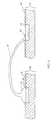
- Fig. 4shows a bonding wire 45 connecting a first bonding pad 20 and a second bonding pad 40 resulting from the method of the present invention.
- the ball or first bond 15is generally formed before the second or stitch bond 65.
- the ball bond 15may be formed by conventional methods as described in the background section.
- the stitch bond 65is formed by a new technique for stitch bonds.
- integrated circuit chips 30 and 55will generally be distinct, it may be desirable for the bonding wire 45 to connect bonding pads 20 and 40 on the same integrated circuit chip.
- the passivation layers 35 and 60are left intact. Therefore, the corrosion and damaged problems associated with conventional methods are avoided.
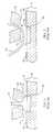
- Fig. 5is a diagrammatic representation of a multi-chip package 80 having bonding wires 45 made in accordance with the method of the present invention.
- all of the bonding wires 45have ball bonds on the two integrated circuit chips 30 and stitch bonds on the integrated circuit chips 55.
- the bonding wires 45may connect bonding pads on the same integrated circuit chips (not shown).
- the chips 30 and 55are all on a die attach pad (DAP) 85.
- DAPdie attach pad
- the integrated circuit chips 30 and 35will be connected to leads 90 of a lead frame to permit electrical connections to external circuitry.
- the stitch bond 65will generally be formed after the formation of the first or ball bond 15.
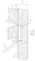
- the bonding capillary 10will be positioned in proximity to the second bonding pad 40 on an integrated chip 55.
- the bonding capillaryis a small conduit which defines a capillary axis 70 along its length.
- the capillary axis 70is aligned with the opening of the bonding capillary 55 through which the bonding wire 45 exudes.
- the opening 55will be circular.
- the capillary tipis also has a face 25 on its distal end which is used as a striking surface during ultrasonic welding.
- the face 25will be assumed to be cylindrically symmetric about the capillary axis 70 and have essentially one face surface about the opening 55.
- a face plane 72can be constructed perpendicular to the capillary axis 70.
- the face surfacewill have a face angle phi ( ⁇ ) with respect to the face plane 72.
- a capillary diameter Dis defined as the projection of the face 25 onto the face plane 72.
- the technique of the inventionis particularly useful when the diameter D of the capillary tip 10 is larger than a width W BP of the second bonding pad 40. In that case, the capillary will be more prone to damage passivation layers 60 surrounding the bonding pad 40.
- the face width W Fhas generally been approximately the same size as the second bonding pad width W BP .
- the capillary tip 10is tilted at an angle theta ( ⁇ ) with respect to a perpendicular 75 to a surface of the second bonding pad 40 as shown in Fig 6.
- the tilt angle theta ( ⁇ )is preferably less than the face angle phi ( ⁇ ). Face angles phi ( ⁇ ) are generally less than about 8° for production bonding machines although other face angles are possible. In a preferred embodiment, the tilt angle theta ( ⁇ ) is less than about 4°.
- the bonding capillary tip 10is tilted generally in the direction of the ball bond 15 formed on the first bonding pad 20.
- a direction vector 77points from the second bonding pad 40 to the first bonding pad 20 (not shown) having the ball bond 15. If the bonding capillary tip 10 were to have moved from the first bonding pad to the second bonding pad in a direct path during the positioning step, the capillary axis 70 would be tilted in a plane (of the page) containing the perpendicular 75 and the direction vector 77 as shown in Fig. 6.
- a welding step of a second end of the bonding wire 45can now be performed without damaging the passivation layer 60.
- the weldingwill be performed by ultrasonic means.
- a bonding wire 45will electrically connect a first bonding pad 20 of a first integrated circuit chip 30 to a second bonding pad 40 of a second integrated circuit chip 55 without the inherit corrosion and circuit damage problems of conventional techniques.
- the wire bonding apparatus 95includes a transducer assembly 100 and a capillary holder 105.
- the capillary holder 105is supported by a table 110 pivotable about a first axis.
- the table 110resides on a second table 115 which is pivotable about a second axis.
- the combination of the first table 110 and the second table 115permits pivoting of the capillary holder 105 and the capillary tip 10 itself about two axes.
- the capillary tip 10is angularly orientable about two axes.
- the transducer assembly 100may be translated using conventional methods used by conventional wiring bonding machines.
- a work holder 120 which supports the integrated circuit chips 30 and 55may be pivotable about one or two axes. In this way, conventional methods for translating the transducer assembly 100 can be used in conjunction with the pivotable work holder 120.
- pivotal work holders 120 or pivoting tables 110 and 115may be constructed.
- the work holder 120may be pivotal about a first axis and the capillary holder 105 and capillary 10 may be pivotal about a second axis by action of the table 115.
- the work holder 120may be translatable while the transducer assembly stays fixed, or the transducer assembly 100 may be translatable relative to a fixed work holder 120.
- the tables 110 and 115 with the work holder 120should be capable of angularly orienting and translating one of the capillary tip 10 and the integrated circuit bonding pads 20 and 40 relative to the other.
- a servo mechanismcan be used to control the angular orientations and translations of the transducer assembly 100, the first table 110, the second table 115, and the work holder 120.
- the wire bonding apparatus 95can form the stitch bonds 65 in two directions at various locations on integrated circuit dies 55.
- the wire bonding apparatuscan also perform ball bonds 15 on tilted bonding pads 20 by tilting the capillary tip 10 to match the tilt of the pad 20.
- the stitch bondmay not occur after the ball bond. It is possible that the ball and stitch bonds may be performed on the same integrated circuit die instead of different ones. Although gold has been described as the wire bonding material, other suitable materials such as aluminum and copper may be used. For some applications, it may be desirable to use face angles of greater than 8° and the tilt angles of greater than 4°. Also, the support for angularly orienting and translating the capillary tip relative to the bonding pads may take a different form than the described tables or pivotal work holder. Additionally, the integrated circuit chips need not all be supported by the same work holder, and the chips may be on other substrates such as jumper chips, connection substrates, or printed circuit boards instead a die attach pad.
- connection substratesmay be used in conjunction with the bonding wires of the present invention.
- the facemay be faceted to form in effect multiple face surfaces about the opening of the bonding capillary.
- the capillary openingmay have a cross section deviating from a circular one such as a square or polygonal cross section.
Landscapes
- Engineering & Computer Science (AREA)
- Computer Hardware Design (AREA)
- Microelectronics & Electronic Packaging (AREA)
- Power Engineering (AREA)
- Manufacturing & Machinery (AREA)
- Mechanical Engineering (AREA)
- Physics & Mathematics (AREA)
- Condensed Matter Physics & Semiconductors (AREA)
- General Physics & Mathematics (AREA)
- Wire Bonding (AREA)
Abstract
Description
- The present invention relates generally to a method of packaging of integrated circuits andmore particularly to bonding wires to integrated circuit bonding pads.
- Semiconductor integrated circuits are currently mass produced for a broad range ofpurposes. Therefore, continual cost and quality improvements in their manufacturer arevaluable and could have broad applicability.
- In recent years, multi-chip modules (MCM's) or multi-chip packages (MCP's)containing more than one integrated circuit die have become widely used because complexcomponents can be made by simply connecting multiple dies to each other within a singlepackage. The terms multi-chip module (MCM) and multi-chip package (MCP) will beconsidered synonymous throughout this application.
- To connect dies to each other in MCP's, one must connect the bonding pads ofdifferent dies. The ball-stitch technique has been of limited use for bonding wires with bothends connected to integrated circuit bonding pads because capillary tips are typically largerin diameter than the bonding pads. The capillary tip can crack the protective passivationlayer(s) surrounding the pads and coating the chip thus permitting corrosion of theintegrated circuit underneath. The tip itself can also damage the integrated circuit whilecracking the passivation layer(s).
- A conventional attempt to use ball-stitch bonding to connect integrated circuitbonding pads to each other is illustrated in Figs. 1-3. Fig. 1 shows a bonding
capillary tip 10 forming aball bond 15 on abonding pad 20. The bondingcapillary tip 10 has aface 25with a face surface. Theface 25 surrounds an opening of the capillary through which awire bonding material exudes to form theball bond 15. Gold is a typical wire bondingmaterial used for making ball bonds. - The
bonding pad 20 resides at a surface of an integratedcircuit chip 30. Althoughthebonding pad 20 is shown as having only two layers, it may normally have four or fivelayers. A layer of thebonding pad 20 may typically be made of an aluminum/siliconcompound. In addition to the bonding pad, theintegrated circuit chip 30 has apassivation layer 35 on itsexterior. Thepassivation layer 35 protects the integrated circuit underneath from damage andcorrosion. If thepassivation layer 35 were to become cracked or damaged, the circuit on theintegratedcircuit chip 30 would be exposed. Additionally, the act of damaging thepassivationlayer 35 could very well damage the substrate beneath the passivation layer and thereforedamage the integrated circuit directly. - After forming the ball or
first bond 15 of a bonding wire as shown in Fig. 1, abonding wire 45 is exuded from the bondingcapillary tip 10 as it is positioned in proximity tosecondbonding pad 40 as shown in Fig. 2. The bondingwire 45 trails out of the opening 50 of thebonding capillary during this positioning step. Generally, in the construction of MCP's, onewants to connect bonding pads of distinct integrated circuit dies. Therefore, thesecondbonding pad 40 has generally been on a second integratedcircuit chip 55 with itsownpassivation layer 60. - Fig. 3 shows a conventional attempt to make a stitch bond on the
second bonding pad 40.Notice that theface 25 of the bondingcapillary tip 10 has penetrated thepassivation layer 60.Thus, the ultrasonic welding of thebonding wire 45 to form astitch bond 65 on thesecondbonding pad 40 will leave a damagedpassivation layer 60 with the concomitant problem of anexposed integrated circuit on thechip 55. - A better method for welding bonding wires to bonding pads with both ball and stitch bondsis desirable. Such a method would permit the usage of a single wire bonding machine to createboth ball and stitch bonds with the same bonding wire. This transference of a techniquepreviously used primarily to connect integrated circuit chips to lead frames will allow one wirebonding machine both to connect multiple integrated circuit chips to each other and to connectchips to a lead frame. If this new technique were to leave the passivation layers intact, thecorrosion and other damage problems caused by current attempts to stitch bond to bondingpads would be obviated.
- European Patent Specification 3270 shows a stitch bonding apparatus in which a planar face surface of a bonding capillary and a bonding pad are angled with respect to one another so thatone side of the bonding capillary face touches the pad first to control the capillary height andcorresponding compression of a wire under the opposite side of the bonding capillary face.The angling may be achieved by an angled face surface or by setting the bonding pad platformand capillary axis at an angle other than perpendicular. EP-534,604 shows an apparatus formaking ball and stitch bonds in which the capillary has an asymmetric tip.
- According to the invention as claimed in claim 1 there is provided a method of bonding a wire to integrated circuitpads using a bonding capillary, the bonding capillary having a bore along the capillary axisterminating in an opening at the tip of the capillary through which a bonding wire exudes andthe tip of the capillary having a face surface surrounding the opening, the method comprisingusing the capillary to form a ball bond by positioning the bonding capillary in proximity to aball bonding pad such that the capillary is substantially perpendicular to the ball bonding padand welding a ball end of the bonding wire exuding out of the capillary opening to the ballbonding pad to form a ball bond, bringing the capillary and exuding wire in to proximity to abonding pad on an integrated circuit die by translating one of the capillary and bonding padwith respect to one another and welding the wire to the surface of the bonding pad to form astitch bond, characterised in that the face surface of the capillary tip is cylindrically symmetricaland angled to recede away from the opening to define a face surface oriented at a face anglewith respect to a face plane perpendicular to the capillary axis, and in that in bringing thecapillary and wire proximate the bonding pad the capillary and die are tilted with respect to oneanother by an angle less than the face angle such that a portion of the face surface overlyingthe bonding wire is rotated towards the bonding pad and the opposite portion of the facesurface is rotated away from the surface of the die to reduce or eliminate contact therewith.
- In this way, a stitch bond can be formed at the bonding pad without damaging the integratedcircuit die.
- This invention should be particularly useful for electrically connecting integrated circuit diesto each other in multi-chip packages (MCP's). In a preferred embodiment, a bonding wire willelectrically connect two dies with a ball bond on one die and a stitch bond on the other diewithout damaging either die.
- The invention, together with further objects and advantages thereof, may best be understoodby reference to the following description taken in conjunction with the accompanying drawingsin which:
- FIGURE 1 is a diagrammatical side cross-section of a capillary tip forming a conventional ballbond to an integrated circuit bonding pad.
- FIGURE 2 is a diagrammatic side cross-section of a capillary tip prior to forming aconventional stitch bond to an integrated circuit bonding pad.
- FIGURE 3 is a diagrammatic side cross-section of a capillary tip forming a conventional stitchbond to an integrated circuit bonding pad.
- FIGURE 4 is a diagrammatic side cross-section of a bonding wire having both a ball bond anda stitch bond and formed by the method of the present invention.
- FIGURE 5 is a perspective view of a multi-chip package with bonding pads connected bywires having ball and stitch bonds.
- FIGURE 6 is a diagrammatic side cross section of a tilted capillary tip positioned inproximity to an integrated circuit bonding pad illustrating positioning and tilting steps of thepresent invention.
- FIGURE 7 is a diagrammatic side cross section of a capillary tip forming a stitchbond to an integrated circuit bonding pad illustrating a welding step of the presentinvention.
- FIGURE 8 is a perspective view of a representation of a wire bonding machine not forming part of the claimedinvention.
- A method for connecting integrated circuit bonding pads by bonding wires havingboth ball and stitch bonds will be disclosed. This technique significantly reduces or obviatethe problems associated with damaged passivation layers and provides reliable stitch wirebonds. The method of the present invention is particularly useful in the manufacturer ofmulti-chip packages (MCP's). In MCP's the integrated circuit chips are generallyconnected to each other as well as being connected to a lead frame.
- Fig. 4 shows a
bonding wire 45 connecting afirst bonding pad 20 and asecondbonding pad 40 resulting from the method of the present invention. The ball orfirst bond 15 is generally formed before the second orstitch bond 65. Theball bond 15 may beformed by conventional methods as described in the background section. However, thestitch bond 65 is formed by a new technique for stitch bonds. Althoughintegrated circuitchips bonding wire 45 toconnectbonding pads passivation layers - Fig. 5 is a diagrammatic representation of a
multi-chip package 80 havingbondingwires 45 made in accordance with the method of the present invention. For illustrativepurposes only, all of thebonding wires 45 have ball bonds on the two integratedcircuitchips 30 and stitch bonds on the integratedcircuit chips 55. As previously noted, thebonding wires 45 may connect bonding pads on the same integrated circuit chips (notshown). In Fig. 5 thechips integrated circuit chips - Beginning with Fig. 6, a method of the invention for forming a
stitch bond 65 on asecond bonding pad 40 will be described in detail. As just described, thestitch bond 65will generally be formed after the formation of the first orball bond 15. In a positioningstep, thebonding capillary 10 will be positioned in proximity to thesecond bonding pad 40on anintegrated chip 55. - Although Fig. 6 shows a dramatic enlargement of a
capillary tip 10, the bondingcapillary is a small conduit which defines acapillary axis 70 along its length. Thecapillaryaxis 70 is aligned with the opening of thebonding capillary 55 through which thebondingwire 45 exudes. In a preferred embodiment, theopening 55 will be circular. The capillarytip is also has aface 25 on its distal end which is used as a striking surface during ultrasonicwelding. For illustrative purposes, theface 25 will be assumed to be cylindricallysymmetric about thecapillary axis 70 and have essentially one face surface about theopening 55. Aface plane 72 can be constructed perpendicular to thecapillary axis 70.Thus defined, the face surface will have a face angle phi () with respect to theface plane 72. - In the art, a capillary diameter D is defined as the projection of the
face 25 onto theface plane 72. The technique of the invention is particularly useful when the diameter D ofthecapillary tip 10 is larger than a width WBP of thesecond bonding pad 40. In that case,the capillary will be more prone to damage passivation layers 60 surrounding thebondingpad 40. - One could also define a face width WF (as shown in Fig. 7) of the capillary tip as alength along the surface of the
face 25 directed radially outward from thecapillary opening 55. For production bonding machines and conventional integrated circuit dies, the facewidth WF has generally been approximately the same size as the second bonding pad widthWBP. - In a tilting step, the
capillary tip 10 is tilted at an angle theta () with respect to aperpendicular 75 to a surface of thesecond bonding pad 40 as shown in Fig 6. The tiltangle theta () is preferably less than the face angle phi (). Face angles phi () aregenerally less than about 8° for production bonding machines although other face angles arepossible. In a preferred embodiment, the tilt angle theta () is less than about 4°. - In another preferred embodiment, the
bonding capillary tip 10 is tilted generally inthe direction of theball bond 15 formed on thefirst bonding pad 20. In Fig. 6 adirectionvector 77 points from thesecond bonding pad 40 to the first bonding pad 20 (not shown)having theball bond 15. If thebonding capillary tip 10 were to have moved from the first bonding pad to the second bonding pad in a direct path during the positioning step, thecapillary axis 70 would be tilted in a plane (of the page) containing the perpendicular 75 andthedirection vector 77 as shown in Fig. 6. - As shown in Fig. 7, by tilting the
bonding capillary tip 10, a welding step of asecond end of thebonding wire 45 can now be performed without damaging thepassivationlayer 60. In a preferred embodiment, the welding will be performed by ultrasonic means.In this way, abonding wire 45 will electrically connect afirst bonding pad 20 of a firstintegrated circuit chip 30 to asecond bonding pad 40 of a secondintegrated circuit chip 55without the inherit corrosion and circuit damage problems of conventional techniques. - A
wire bonding apparatus 95 suitable for forming the ball bonds and the stitchbonds not forming part of the claimed invention is shown in Fig. 8. Thewire bondingapparatus 95 includes atransducer assembly 100 and acapillary holder 105. In a preferredembodiment, thecapillary holder 105 is supported by a table 110 pivotable about a firstaxis. In another preferred embodiment, the table 110 resides on a second table 115 whichis pivotable about a second axis. The combination of the first table 110 and the second table115 permits pivoting of thecapillary holder 105 and thecapillary tip 10 itself about twoaxes. Thus, thecapillary tip 10 is angularly orientable about two axes. Thetransducerassembly 100 may be translated using conventional methods used by conventional wiringbonding machines. - Alternatively, a
work holder 120 which supports theintegrated circuit chips transducer assembly 100 can be used in conjunction with thepivotable workholder 120. - Alternatively, other combinations of
pivotal work holders 120 or pivoting tables 110and 115 may be constructed. For example, thework holder 120 may be pivotal about afirst axis and thecapillary holder 105 and capillary 10 may be pivotal about a second axisby action of the table 115. Likewise, thework holder 120 may be translatable while thetransducer assembly stays fixed, or thetransducer assembly 100 may be translatable relativeto afixed work holder 120. Collectively, the tables 110 and 115 with thework holder 120should be capable of angularly orienting and translating one of thecapillary tip 10 and theintegratedcircuit bonding pads transducer assembly 100, the first table 110, the second table 115, and thework holder 120. - By translating the
capillary tip 10 and pivoting the tip about two axes, thewirebonding apparatus 95 can form thestitch bonds 65 in two directions at various locations onintegrated circuit dies 55. The wire bonding apparatus can also performball bonds 15 ontiltedbonding pads 20 by tilting thecapillary tip 10 to match the tilt of thepad 20. - The stitchbond may not occur after the ball bond. It is possible that the ball and stitch bonds may beperformed on the same integrated circuit die instead of different ones. Although gold hasbeen described as the wire bonding material, other suitable materials such as aluminum andcopper may be used. For some applications, it may be desirable to use face angles ofgreater than 8° and the tilt angles of greater than 4°. Also, the support for angularlyorienting and translating the capillary tip relative to the bonding pads may take a differentform than the described tables or pivotal work holder. Additionally, the integrated circuitchips need not all be supported by the same work holder, and the chips may be on othersubstrates such as jumper chips, connection substrates, or printed circuit boards instead adie attach pad. Other connections between integrated circuit chips such as through jumperchips and connection substrates may be used in conjunction with the bonding wires of thepresent invention. The face may be faceted to form in effect multiple face surfaces about theopening of the bonding capillary. Additionally, the capillary opening may have a crosssection deviating from a circular one such as a square or polygonal cross section.
Claims (5)
- A method of bonding a wire (45) to integrated circuit pads (20, 40) using a bondingcapillary (10), the bonding capillary having a bore along the capillary axis terminating in anopening at the tip of the capillary through which a bonding wire exudes and the tip of thecapillary having a face surface (25) surrounding the opening,characterised in that the face surface of the capillary tip is cylindrically symmetrical and angledto recede away from the opening to define a face surface oriented at a face angle with respectto a face plane perpendicular to the capillary axis, andin that in bringing the capillary and wireproximate the bonding pad the capillary and die are tilted with respect to one another by anangle less than the face angle but greater than zero such that a portion of the face surface overlying the bonding wireis rotated towards the bonding pad and the opposite portion of the face surface is rotated awayfrom the surface of the die to reduce or eliminate contact therewith.the method comprising using the capillary to form a ball bond by positioning the bondingcapillary in proximity to a ball bonding pad (20) such that the capillary is substantiallyperpendicular to the ball bonding pad and welding a ball end of the bonding wire exuding outof the capillary opening to the ball bonding pad to form a ball bond,bringing the capillary and exuding wire in to proximity to a bonding pad (40) on an integratedcircuit die by translating one of the capillary and bonding pad with respect to one another andwelding the wire to the surface of the bonding pad to form a stitch bond (65),
- A method according to claim 1 wherein the ball bonding pad and the bonding pad for thestitch bond are on separate integrated circuit dies.
- A method according to any preceding claim in which the tilting is of the top of the capillaryaxis in the direction towards the first bonding pad.
- A method according to any preceding claim in which the face surface capillary tip is angled away from the opening by less than 8°.
- A method according to any preceding claim in which the die and capillary are tilted in therange of 0° to 4°.
Applications Claiming Priority (3)
| Application Number | Priority Date | Filing Date | Title |
|---|---|---|---|
| US08/293,822US5437405A (en) | 1994-08-22 | 1994-08-22 | Method and apparatus for stitch bonding of wires to integrated circuit bonding pads |
| PCT/US1995/010719WO1996006455A1 (en) | 1994-08-22 | 1995-08-17 | Method and apparatus for stitch bonding of wires to integrated circuit bonding pads |
| US293822 | 1999-04-16 |
Publications (2)
| Publication Number | Publication Date |
|---|---|
| EP0724776A1 EP0724776A1 (en) | 1996-08-07 |
| EP0724776B1true EP0724776B1 (en) | 2001-10-31 |
Family
ID=23130741
Family Applications (1)
| Application Number | Title | Priority Date | Filing Date |
|---|---|---|---|
| EP95930924AExpired - LifetimeEP0724776B1 (en) | 1994-08-22 | 1995-08-17 | Method for stitch bonding of wires to integrated circuit bonding pads |
Country Status (5)
| Country | Link |
|---|---|
| US (1) | US5437405A (en) |
| EP (1) | EP0724776B1 (en) |
| KR (1) | KR100349727B1 (en) |
| DE (1) | DE69523557T2 (en) |
| WO (1) | WO1996006455A1 (en) |
Families Citing this family (26)
| Publication number | Priority date | Publication date | Assignee | Title |
|---|---|---|---|---|
| US5702049A (en)* | 1995-06-07 | 1997-12-30 | West Bond Inc. | Angled wire bonding tool and alignment method |
| US5813590A (en)* | 1995-12-18 | 1998-09-29 | Micron Technology, Inc. | Extended travel wire bonding machine |
| US5843809A (en)* | 1996-01-24 | 1998-12-01 | Lsi Logic Corporation | Lead frames for trench drams |
| US5938105A (en)* | 1997-01-15 | 1999-08-17 | National Semiconductor Corporation | Encapsulated ball bonding apparatus and method |
| US6065667A (en)* | 1997-01-15 | 2000-05-23 | National Semiconductor Corporation | Method and apparatus for fine pitch wire bonding |
| WO1999033100A1 (en)* | 1997-12-19 | 1999-07-01 | Toto Ltd. | Wire bonding capillary |
| JP2000082717A (en)* | 1998-09-07 | 2000-03-21 | Shinkawa Ltd | Wire bonding method |
| US6158647A (en)* | 1998-09-29 | 2000-12-12 | Micron Technology, Inc. | Concave face wire bond capillary |
| JP4010432B2 (en)* | 1999-01-29 | 2007-11-21 | ローム株式会社 | Wire bonding method and apparatus for electronic parts |
| US20080197172A1 (en)* | 1999-02-25 | 2008-08-21 | Reiber Steven F | Bonding Tool |
| US7389905B2 (en)* | 1999-02-25 | 2008-06-24 | Reiber Steven F | Flip chip bonding tool tip |
| US20070131661A1 (en)* | 1999-02-25 | 2007-06-14 | Reiber Steven F | Solder ball placement system |
| US7124927B2 (en)* | 1999-02-25 | 2006-10-24 | Reiber Steven F | Flip chip bonding tool and ball placement capillary |
| US20060261132A1 (en)* | 1999-02-25 | 2006-11-23 | Reiber Steven F | Low range bonding tool |
| US6910612B2 (en)* | 2001-07-17 | 2005-06-28 | Kulicke & Soffa Investments, Inc. | Capillary with contained inner chamfer |
| US6715658B2 (en)* | 2001-07-17 | 2004-04-06 | Kulicke & Soffa Investments, Inc. | Ultra fine pitch capillary |
| US20040036171A1 (en)* | 2002-08-22 | 2004-02-26 | Farnworth Warren M. | Method and apparatus for enabling a stitch wire bond in the absence of discrete bump formation, semiconductor device assemblies and electronic systems including same |
| JP3765778B2 (en)* | 2002-08-29 | 2006-04-12 | ローム株式会社 | Capillary for wire bonding and wire bonding method using the same |
| US7249702B2 (en)* | 2003-12-04 | 2007-07-31 | Kulicke And Soffa Industries, Inc. | Multi-part capillary |
| US20070085085A1 (en)* | 2005-08-08 | 2007-04-19 | Reiber Steven F | Dissipative pick and place tools for light wire and LED displays |
| US20070296056A1 (en)* | 2006-06-27 | 2007-12-27 | Texas Instruments Incorporated | Integrated Circuits Having Controlled Inductances |
| JP4596011B2 (en)* | 2008-01-09 | 2010-12-08 | トヨタ自動車株式会社 | Semiconductor device |
| JP4625858B2 (en)* | 2008-09-10 | 2011-02-02 | 株式会社カイジョー | Wire bonding method, wire bonding apparatus, and wire bonding control program |
| KR20140135319A (en)* | 2013-05-15 | 2014-11-26 | 삼성전자주식회사 | Wire-bonding method and semiconductor package formed by using the method |
| CN110100314B (en)* | 2017-06-09 | 2022-08-09 | 富士电机株式会社 | Semiconductor device and method for manufacturing semiconductor device |
| JP7679289B2 (en)* | 2020-12-23 | 2025-05-19 | スカイワークス ソリューションズ,インコーポレイテッド | Apparatus and method for tool mark free stitch bonding - Patents.com |
Family Cites Families (8)
| Publication number | Priority date | Publication date | Assignee | Title |
|---|---|---|---|---|
| FR2412943A1 (en)* | 1977-12-20 | 1979-07-20 | Thomson Csf | PROCESS FOR MAKING CONNECTIONS OF A SEMICONDUCTOR DEVICE ON A BASE, APPARATUS FOR IMPLEMENTING THE PROCESS, AND SEMICONDUCTOR DEVICE OBTAINED BY THIS PROCESS |
| US4475681A (en)* | 1982-05-24 | 1984-10-09 | The Micromanipulator Co., Inc. | Bonder apparatus |
| FR2555813B1 (en)* | 1983-09-28 | 1986-06-20 | Hitachi Ltd | SEMICONDUCTOR DEVICE AND METHOD FOR MANUFACTURING SUCH A DEVICE |
| JPH0734449B2 (en)* | 1987-11-30 | 1995-04-12 | 三菱電機株式会社 | Electrode junction structure of semiconductor device |
| JPH01273325A (en)* | 1988-04-25 | 1989-11-01 | Toshiba Corp | Manufacture of capillary and semiconductor device using the capillary |
| JPH02125631A (en)* | 1988-11-04 | 1990-05-14 | Hitachi Ltd | Semiconductor device, manufacturing method thereof, and wire bonding device used therein |
| US5111989A (en)* | 1991-09-26 | 1992-05-12 | Kulicke And Soffa Investments, Inc. | Method of making low profile fine wire interconnections |
| US5328079A (en)* | 1993-03-19 | 1994-07-12 | National Semiconductor Corporation | Method of and arrangement for bond wire connecting together certain integrated circuit components |
- 1994
- 1994-08-22USUS08/293,822patent/US5437405A/ennot_activeExpired - Lifetime
- 1995
- 1995-08-17WOPCT/US1995/010719patent/WO1996006455A1/enactiveIP Right Grant
- 1995-08-17EPEP95930924Apatent/EP0724776B1/ennot_activeExpired - Lifetime
- 1995-08-17DEDE69523557Tpatent/DE69523557T2/ennot_activeExpired - Fee Related
- 1995-08-17KRKR1019960702058Apatent/KR100349727B1/ennot_activeExpired - Fee Related
Also Published As
| Publication number | Publication date |
|---|---|
| EP0724776A1 (en) | 1996-08-07 |
| DE69523557T2 (en) | 2002-08-08 |
| KR100349727B1 (en) | 2002-12-26 |
| US5437405A (en) | 1995-08-01 |
| KR960706189A (en) | 1996-11-08 |
| DE69523557D1 (en) | 2001-12-06 |
| WO1996006455A1 (en) | 1996-02-29 |
Similar Documents
| Publication | Publication Date | Title |
|---|---|---|
| EP0724776B1 (en) | Method for stitch bonding of wires to integrated circuit bonding pads | |
| US5465899A (en) | Method and apparatus for fine pitch wire bonding using a shaved capillary | |
| JP4860128B2 (en) | Wire bonding method | |
| JP2004221257A (en) | Wire bonding method and wire bonding apparatus | |
| US7021520B2 (en) | Stacked chip connection using stand off stitch bonding | |
| JPH02123685A (en) | Method of bonding wire containing gold with solder | |
| US6112973A (en) | Angled transducer-dual head bonder for optimum ultrasonic power application and flexibility for tight pitch leadframe | |
| US5495976A (en) | Tilted wedge bonding tool | |
| JPH10512399A (en) | Method for electrically connecting a semiconductor chip to at least one contact surface | |
| JPH05326601A (en) | Wire bonding method | |
| JPH04255237A (en) | Manufacturing method of semiconductor device | |
| US6076686A (en) | Support structure for use during package removal from a multi-layer integrated circuit device | |
| JP2000174047A (en) | Flip chip package bump forming method, bonding tool and flip chip package component | |
| JP3202193B2 (en) | Wire bonding method | |
| JPH11214424A (en) | Wedge bonding method and apparatus, and semiconductor device | |
| KR200292328Y1 (en) | Semiconductor package | |
| JPH10125710A (en) | Wire bonding | |
| US6131792A (en) | Balancing of x and y axis bonding by 45 degree capillary positioning | |
| JPS61117847A (en) | Formation of bonding metallic projection | |
| JPH08250545A (en) | Semiconductor device and manufacture thereof | |
| JP2000012598A (en) | Capillary, wire bonding method and apparatus using the same, and method of manufacturing semiconductor device | |
| JPH05326609A (en) | Wire bonder and bonding method for semiconductor device | |
| JPH0611066B2 (en) | Wire bonding equipment | |
| JPH02277251A (en) | Wire bonding method and device | |
| JPH04256330A (en) | Wire bonding method and wire bonding device |
Legal Events
| Date | Code | Title | Description |
|---|---|---|---|
| PUAI | Public reference made under article 153(3) epc to a published international application that has entered the european phase | Free format text:ORIGINAL CODE: 0009012 | |
| 17P | Request for examination filed | Effective date:19960503 | |
| AK | Designated contracting states | Kind code of ref document:A1 Designated state(s):DE FR GB | |
| 17Q | First examination report despatched | Effective date:19961204 | |
| RIC1 | Information provided on ipc code assigned before grant | Free format text:7H 01L 21/607 A, 7H 01L 21/603 B | |
| RTI1 | Title (correction) | Free format text:METHOD FOR STITCH BONDING OF WIRES TO INTEGRATED CIRCUIT BONDING PADS | |
| GRAG | Despatch of communication of intention to grant | Free format text:ORIGINAL CODE: EPIDOS AGRA | |
| GRAG | Despatch of communication of intention to grant | Free format text:ORIGINAL CODE: EPIDOS AGRA | |
| GRAH | Despatch of communication of intention to grant a patent | Free format text:ORIGINAL CODE: EPIDOS IGRA | |
| GRAH | Despatch of communication of intention to grant a patent | Free format text:ORIGINAL CODE: EPIDOS IGRA | |
| GRAA | (expected) grant | Free format text:ORIGINAL CODE: 0009210 | |
| AK | Designated contracting states | Kind code of ref document:B1 Designated state(s):DE FR GB | |
| PG25 | Lapsed in a contracting state [announced via postgrant information from national office to epo] | Ref country code:FR Free format text:LAPSE BECAUSE OF FAILURE TO SUBMIT A TRANSLATION OF THE DESCRIPTION OR TO PAY THE FEE WITHIN THE PRESCRIBED TIME-LIMIT Effective date:20011031 | |
| REF | Corresponds to: | Ref document number:69523557 Country of ref document:DE Date of ref document:20011206 | |
| REG | Reference to a national code | Ref country code:GB Ref legal event code:IF02 | |
| PG25 | Lapsed in a contracting state [announced via postgrant information from national office to epo] | Ref country code:GB Free format text:LAPSE BECAUSE OF NON-PAYMENT OF DUE FEES Effective date:20020817 | |
| PLBE | No opposition filed within time limit | Free format text:ORIGINAL CODE: 0009261 | |
| STAA | Information on the status of an ep patent application or granted ep patent | Free format text:STATUS: NO OPPOSITION FILED WITHIN TIME LIMIT | |
| 26N | No opposition filed | ||
| GBPC | Gb: european patent ceased through non-payment of renewal fee | Effective date:20020817 | |
| PGFP | Annual fee paid to national office [announced via postgrant information from national office to epo] | Ref country code:DE Payment date:20071001 Year of fee payment:13 | |
| PG25 | Lapsed in a contracting state [announced via postgrant information from national office to epo] | Ref country code:DE Free format text:LAPSE BECAUSE OF NON-PAYMENT OF DUE FEES Effective date:20090303 |