EP0720225B1 - Lateral power MOSFET having metal strap layer to reduce distributed resistance and method of fabricating the same - Google Patents
Lateral power MOSFET having metal strap layer to reduce distributed resistance and method of fabricating the sameDownload PDFInfo
- Publication number
- EP0720225B1 EP0720225B1EP95309533AEP95309533AEP0720225B1EP 0720225 B1EP0720225 B1EP 0720225B1EP 95309533 AEP95309533 AEP 95309533AEP 95309533 AEP95309533 AEP 95309533AEP 0720225 B1EP0720225 B1EP 0720225B1
- Authority
- EP
- European Patent Office
- Prior art keywords
- layer
- conductive line
- metal
- integrated circuit
- metal strap
- Prior art date
- Legal status (The legal status is an assumption and is not a legal conclusion. Google has not performed a legal analysis and makes no representation as to the accuracy of the status listed.)
- Expired - Lifetime
Links
- 229910052751metalInorganic materials0.000titleclaimsdescription174
- 239000002184metalSubstances0.000titleclaimsdescription174
- 238000004519manufacturing processMethods0.000titledescription5
- 239000010410layerSubstances0.000claimsdescription195
- 238000002161passivationMethods0.000claimsdescription34
- 238000000034methodMethods0.000claimsdescription30
- PXHVJJICTQNCMI-UHFFFAOYSA-NNickelChemical compound[Ni]PXHVJJICTQNCMI-UHFFFAOYSA-N0.000claimsdescription28
- PCHJSUWPFVWCPO-UHFFFAOYSA-NgoldChemical compound[Au]PCHJSUWPFVWCPO-UHFFFAOYSA-N0.000claimsdescription20
- 229910052737goldInorganic materials0.000claimsdescription20
- 239000010931goldSubstances0.000claimsdescription20
- 229910052759nickelInorganic materials0.000claimsdescription14
- 238000000151depositionMethods0.000claimsdescription13
- 239000000758substrateSubstances0.000claimsdescription12
- HCHKCACWOHOZIP-UHFFFAOYSA-NZincChemical compound[Zn]HCHKCACWOHOZIP-UHFFFAOYSA-N0.000claimsdescription10
- RTAQQCXQSZGOHL-UHFFFAOYSA-NTitaniumChemical compound[Ti]RTAQQCXQSZGOHL-UHFFFAOYSA-N0.000claimsdescription9
- 238000005530etchingMethods0.000claimsdescription9
- 229910052719titaniumInorganic materials0.000claimsdescription9
- 239000010936titaniumSubstances0.000claimsdescription9
- 229910052725zincInorganic materials0.000claimsdescription9
- 239000011701zincSubstances0.000claimsdescription9
- 229910052782aluminiumInorganic materials0.000claimsdescription4
- XAGFODPZIPBFFR-UHFFFAOYSA-NaluminiumChemical compound[Al]XAGFODPZIPBFFR-UHFFFAOYSA-N0.000claimsdescription4
- 239000000463materialSubstances0.000claimsdescription3
- 238000007747platingMethods0.000claims4
- 239000004065semiconductorSubstances0.000claims3
- 239000002344surface layerSubstances0.000claims3
- 210000000746body regionAnatomy0.000description7
- 229910021420polycrystalline siliconInorganic materials0.000description7
- 229920005591polysiliconPolymers0.000description7
- XUIMIQQOPSSXEZ-UHFFFAOYSA-NSiliconChemical compound[Si]XUIMIQQOPSSXEZ-UHFFFAOYSA-N0.000description4
- 238000013461designMethods0.000description4
- 238000009792diffusion processMethods0.000description4
- 239000007943implantSubstances0.000description4
- 229910052710siliconInorganic materials0.000description4
- 239000010703siliconSubstances0.000description4
- KRHYYFGTRYWZRS-UHFFFAOYSA-NFluoraneChemical compoundFKRHYYFGTRYWZRS-UHFFFAOYSA-N0.000description3
- -1aluminum-copper-siliconChemical compound0.000description3
- 230000008901benefitEffects0.000description3
- 230000015572biosynthetic processEffects0.000description3
- 239000002019doping agentSubstances0.000description3
- 230000000694effectsEffects0.000description3
- 239000011521glassSubstances0.000description3
- 238000012545processingMethods0.000description3
- VEXZGXHMUGYJMC-UHFFFAOYSA-NHydrochloric acidChemical compoundClVEXZGXHMUGYJMC-UHFFFAOYSA-N0.000description2
- BQCADISMDOOEFD-UHFFFAOYSA-NSilverChemical compound[Ag]BQCADISMDOOEFD-UHFFFAOYSA-N0.000description2
- QAOWNCQODCNURD-UHFFFAOYSA-NSulfuric acidChemical compoundOS(O)(=O)=OQAOWNCQODCNURD-UHFFFAOYSA-N0.000description2
- 229910052796boronInorganic materials0.000description2
- 239000004020conductorSubstances0.000description2
- 238000005336crackingMethods0.000description2
- 230000008021depositionEffects0.000description2
- 238000010586diagramMethods0.000description2
- 238000007772electroless platingMethods0.000description2
- 238000009713electroplatingMethods0.000description2
- 239000011229interlayerSubstances0.000description2
- 229910021645metal ionInorganic materials0.000description2
- 238000012856packingMethods0.000description2
- 230000003071parasitic effectEffects0.000description2
- 229920002120photoresistant polymerPolymers0.000description2
- BASFCYQUMIYNBI-UHFFFAOYSA-NplatinumChemical compound[Pt]BASFCYQUMIYNBI-UHFFFAOYSA-N0.000description2
- 230000009467reductionEffects0.000description2
- 229910052709silverInorganic materials0.000description2
- 239000004332silverSubstances0.000description2
- 239000002356single layerSubstances0.000description2
- 125000006850spacer groupChemical group0.000description2
- XLYOFNOQVPJJNP-UHFFFAOYSA-NwaterSubstancesOXLYOFNOQVPJJNP-UHFFFAOYSA-N0.000description2
- ZOXJGFHDIHLPTG-UHFFFAOYSA-NBoronChemical compound[B]ZOXJGFHDIHLPTG-UHFFFAOYSA-N0.000description1
- 241000282461Canis lupusSpecies0.000description1
- XFXPMWWXUTWYJX-UHFFFAOYSA-NCyanideChemical compoundN#[C-]XFXPMWWXUTWYJX-UHFFFAOYSA-N0.000description1
- 241000206607Porphyra umbilicalisSpecies0.000description1
- 229910052581Si3N4Inorganic materials0.000description1
- QFSBUAQADJMBQB-UHFFFAOYSA-J[Ni+4].P(=O)([O-])([O-])P(=O)([O-])[O-]Chemical compound[Ni+4].P(=O)([O-])([O-])P(=O)([O-])[O-]QFSBUAQADJMBQB-UHFFFAOYSA-J0.000description1
- CSDREXVUYHZDNP-UHFFFAOYSA-NalumanylidynesiliconChemical compound[Al].[Si]CSDREXVUYHZDNP-UHFFFAOYSA-N0.000description1
- 229910052787antimonyInorganic materials0.000description1
- WATWJIUSRGPENY-UHFFFAOYSA-Nantimony atomChemical compound[Sb]WATWJIUSRGPENY-UHFFFAOYSA-N0.000description1
- 239000005380borophosphosilicate glassSubstances0.000description1
- 238000005229chemical vapour depositionMethods0.000description1
- 230000000295complement effectEffects0.000description1
- 239000002131composite materialSubstances0.000description1
- 235000014510cookyNutrition0.000description1
- 230000007423decreaseEffects0.000description1
- 238000011982device technologyMethods0.000description1
- 238000001312dry etchingMethods0.000description1
- 239000002355dual-layerSubstances0.000description1
- 230000008020evaporationEffects0.000description1
- 238000001704evaporationMethods0.000description1
- 238000010438heat treatmentMethods0.000description1
- 238000002513implantationMethods0.000description1
- 150000002500ionsChemical class0.000description1
- 238000002955isolationMethods0.000description1
- 238000001465metallisationMethods0.000description1
- QPJSUIGXIBEQAC-UHFFFAOYSA-Nn-(2,4-dichloro-5-propan-2-yloxyphenyl)acetamideChemical compoundCC(C)OC1=CC(NC(C)=O)=C(Cl)C=C1ClQPJSUIGXIBEQAC-UHFFFAOYSA-N0.000description1
- 150000004767nitridesChemical class0.000description1
- 238000009828non-uniform distributionMethods0.000description1
- 230000003647oxidationEffects0.000description1
- 238000007254oxidation reactionMethods0.000description1
- 238000004806packaging method and processMethods0.000description1
- 229910052697platinumInorganic materials0.000description1
- 230000002028prematureEffects0.000description1
- 238000007665saggingMethods0.000description1
- HQVNEWCFYHHQES-UHFFFAOYSA-Nsilicon nitrideChemical compoundN12[Si]34N5[Si]62N3[Si]51N64HQVNEWCFYHHQES-UHFFFAOYSA-N0.000description1
- 238000004544sputter depositionMethods0.000description1
- 239000000126substanceSubstances0.000description1
- 239000002699waste materialSubstances0.000description1
- 238000001039wet etchingMethods0.000description1
- NWONKYPBYAMBJT-UHFFFAOYSA-Lzinc sulfateChemical compound[Zn+2].[O-]S([O-])(=O)=ONWONKYPBYAMBJT-UHFFFAOYSA-L0.000description1
Images


Classifications
- H—ELECTRICITY
- H01—ELECTRIC ELEMENTS
- H01L—SEMICONDUCTOR DEVICES NOT COVERED BY CLASS H10
- H01L24/00—Arrangements for connecting or disconnecting semiconductor or solid-state bodies; Methods or apparatus related thereto
- H01L24/01—Means for bonding being attached to, or being formed on, the surface to be connected, e.g. chip-to-package, die-attach, "first-level" interconnects; Manufacturing methods related thereto
- H01L24/02—Bonding areas ; Manufacturing methods related thereto
- H01L24/04—Structure, shape, material or disposition of the bonding areas prior to the connecting process
- H01L24/06—Structure, shape, material or disposition of the bonding areas prior to the connecting process of a plurality of bonding areas
- H—ELECTRICITY
- H01—ELECTRIC ELEMENTS
- H01L—SEMICONDUCTOR DEVICES NOT COVERED BY CLASS H10
- H01L23/00—Details of semiconductor or other solid state devices
- H01L23/48—Arrangements for conducting electric current to or from the solid state body in operation, e.g. leads, terminal arrangements ; Selection of materials therefor
- H01L23/482—Arrangements for conducting electric current to or from the solid state body in operation, e.g. leads, terminal arrangements ; Selection of materials therefor consisting of lead-in layers inseparably applied to the semiconductor body (electrodes)
- H01L23/4824—Pads with extended contours, e.g. grid structure, branch structure, finger structure
- H—ELECTRICITY
- H01—ELECTRIC ELEMENTS
- H01L—SEMICONDUCTOR DEVICES NOT COVERED BY CLASS H10
- H01L24/00—Arrangements for connecting or disconnecting semiconductor or solid-state bodies; Methods or apparatus related thereto
- H01L24/01—Means for bonding being attached to, or being formed on, the surface to be connected, e.g. chip-to-package, die-attach, "first-level" interconnects; Manufacturing methods related thereto
- H01L24/02—Bonding areas ; Manufacturing methods related thereto
- H01L24/03—Manufacturing methods
- H—ELECTRICITY
- H01—ELECTRIC ELEMENTS
- H01L—SEMICONDUCTOR DEVICES NOT COVERED BY CLASS H10
- H01L24/00—Arrangements for connecting or disconnecting semiconductor or solid-state bodies; Methods or apparatus related thereto
- H01L24/01—Means for bonding being attached to, or being formed on, the surface to be connected, e.g. chip-to-package, die-attach, "first-level" interconnects; Manufacturing methods related thereto
- H01L24/02—Bonding areas ; Manufacturing methods related thereto
- H01L24/04—Structure, shape, material or disposition of the bonding areas prior to the connecting process
- H01L24/05—Structure, shape, material or disposition of the bonding areas prior to the connecting process of an individual bonding area
- H—ELECTRICITY
- H01—ELECTRIC ELEMENTS
- H01L—SEMICONDUCTOR DEVICES NOT COVERED BY CLASS H10
- H01L24/00—Arrangements for connecting or disconnecting semiconductor or solid-state bodies; Methods or apparatus related thereto
- H01L24/01—Means for bonding being attached to, or being formed on, the surface to be connected, e.g. chip-to-package, die-attach, "first-level" interconnects; Manufacturing methods related thereto
- H01L24/42—Wire connectors; Manufacturing methods related thereto
- H01L24/47—Structure, shape, material or disposition of the wire connectors after the connecting process
- H01L24/48—Structure, shape, material or disposition of the wire connectors after the connecting process of an individual wire connector
- H—ELECTRICITY
- H10—SEMICONDUCTOR DEVICES; ELECTRIC SOLID-STATE DEVICES NOT OTHERWISE PROVIDED FOR
- H10D—INORGANIC ELECTRIC SEMICONDUCTOR DEVICES
- H10D30/00—Field-effect transistors [FET]
- H10D30/60—Insulated-gate field-effect transistors [IGFET]
- H10D30/601—Insulated-gate field-effect transistors [IGFET] having lightly-doped drain or source extensions, e.g. LDD IGFETs or DDD IGFETs
- H10D30/603—Insulated-gate field-effect transistors [IGFET] having lightly-doped drain or source extensions, e.g. LDD IGFETs or DDD IGFETs having asymmetry in the channel direction, e.g. lateral high-voltage MISFETs having drain offset region or extended drain IGFETs [EDMOS]
- H—ELECTRICITY
- H10—SEMICONDUCTOR DEVICES; ELECTRIC SOLID-STATE DEVICES NOT OTHERWISE PROVIDED FOR
- H10D—INORGANIC ELECTRIC SEMICONDUCTOR DEVICES
- H10D30/00—Field-effect transistors [FET]
- H10D30/60—Insulated-gate field-effect transistors [IGFET]
- H10D30/64—Double-diffused metal-oxide semiconductor [DMOS] FETs
- H10D30/66—Vertical DMOS [VDMOS] FETs
- H10D30/663—Vertical DMOS [VDMOS] FETs having both source contacts and drain contacts on the same surface, i.e. up-drain VDMOS
- H—ELECTRICITY
- H10—SEMICONDUCTOR DEVICES; ELECTRIC SOLID-STATE DEVICES NOT OTHERWISE PROVIDED FOR
- H10D—INORGANIC ELECTRIC SEMICONDUCTOR DEVICES
- H10D62/00—Semiconductor bodies, or regions thereof, of devices having potential barriers
- H10D62/10—Shapes, relative sizes or dispositions of the regions of the semiconductor bodies; Shapes of the semiconductor bodies
- H10D62/17—Semiconductor regions connected to electrodes not carrying current to be rectified, amplified or switched, e.g. channel regions
- H10D62/213—Channel regions of field-effect devices
- H10D62/221—Channel regions of field-effect devices of FETs
- H10D62/235—Channel regions of field-effect devices of FETs of IGFETs
- H10D62/299—Channel regions of field-effect devices of FETs of IGFETs having lateral doping variations
- H10D62/307—Channel regions of field-effect devices of FETs of IGFETs having lateral doping variations the doping variations being parallel to the channel lengths
- H—ELECTRICITY
- H10—SEMICONDUCTOR DEVICES; ELECTRIC SOLID-STATE DEVICES NOT OTHERWISE PROVIDED FOR
- H10D—INORGANIC ELECTRIC SEMICONDUCTOR DEVICES
- H10D64/00—Electrodes of devices having potential barriers
- H10D64/20—Electrodes characterised by their shapes, relative sizes or dispositions
- H10D64/23—Electrodes carrying the current to be rectified, amplified, oscillated or switched, e.g. sources, drains, anodes or cathodes
- H10D64/251—Source or drain electrodes for field-effect devices
- H10D64/252—Source or drain electrodes for field-effect devices for vertical or pseudo-vertical devices
- H—ELECTRICITY
- H10—SEMICONDUCTOR DEVICES; ELECTRIC SOLID-STATE DEVICES NOT OTHERWISE PROVIDED FOR
- H10D—INORGANIC ELECTRIC SEMICONDUCTOR DEVICES
- H10D64/00—Electrodes of devices having potential barriers
- H10D64/20—Electrodes characterised by their shapes, relative sizes or dispositions
- H10D64/23—Electrodes carrying the current to be rectified, amplified, oscillated or switched, e.g. sources, drains, anodes or cathodes
- H10D64/251—Source or drain electrodes for field-effect devices
- H10D64/257—Source or drain electrodes for field-effect devices for lateral devices wherein the source or drain electrodes are characterised by top-view geometrical layouts, e.g. interdigitated, semi-circular, annular or L-shaped electrodes
- H—ELECTRICITY
- H01—ELECTRIC ELEMENTS
- H01L—SEMICONDUCTOR DEVICES NOT COVERED BY CLASS H10
- H01L2224/00—Indexing scheme for arrangements for connecting or disconnecting semiconductor or solid-state bodies and methods related thereto as covered by H01L24/00
- H01L2224/01—Means for bonding being attached to, or being formed on, the surface to be connected, e.g. chip-to-package, die-attach, "first-level" interconnects; Manufacturing methods related thereto
- H01L2224/02—Bonding areas; Manufacturing methods related thereto
- H01L2224/04—Structure, shape, material or disposition of the bonding areas prior to the connecting process
- H01L2224/04042—Bonding areas specifically adapted for wire connectors, e.g. wirebond pads
- H—ELECTRICITY
- H01—ELECTRIC ELEMENTS
- H01L—SEMICONDUCTOR DEVICES NOT COVERED BY CLASS H10
- H01L2224/00—Indexing scheme for arrangements for connecting or disconnecting semiconductor or solid-state bodies and methods related thereto as covered by H01L24/00
- H01L2224/01—Means for bonding being attached to, or being formed on, the surface to be connected, e.g. chip-to-package, die-attach, "first-level" interconnects; Manufacturing methods related thereto
- H01L2224/02—Bonding areas; Manufacturing methods related thereto
- H01L2224/04—Structure, shape, material or disposition of the bonding areas prior to the connecting process
- H01L2224/05—Structure, shape, material or disposition of the bonding areas prior to the connecting process of an individual bonding area
- H01L2224/05001—Internal layers
- H01L2224/05099—Material
- H01L2224/051—Material with a principal constituent of the material being a metal or a metalloid, e.g. boron [B], silicon [Si], germanium [Ge], arsenic [As], antimony [Sb], tellurium [Te] and polonium [Po], and alloys thereof
- H01L2224/05138—Material with a principal constituent of the material being a metal or a metalloid, e.g. boron [B], silicon [Si], germanium [Ge], arsenic [As], antimony [Sb], tellurium [Te] and polonium [Po], and alloys thereof the principal constituent melting at a temperature of greater than or equal to 950°C and less than 1550°C
- H01L2224/05155—Nickel [Ni] as principal constituent
- H—ELECTRICITY
- H01—ELECTRIC ELEMENTS
- H01L—SEMICONDUCTOR DEVICES NOT COVERED BY CLASS H10
- H01L2224/00—Indexing scheme for arrangements for connecting or disconnecting semiconductor or solid-state bodies and methods related thereto as covered by H01L24/00
- H01L2224/01—Means for bonding being attached to, or being formed on, the surface to be connected, e.g. chip-to-package, die-attach, "first-level" interconnects; Manufacturing methods related thereto
- H01L2224/02—Bonding areas; Manufacturing methods related thereto
- H01L2224/04—Structure, shape, material or disposition of the bonding areas prior to the connecting process
- H01L2224/05—Structure, shape, material or disposition of the bonding areas prior to the connecting process of an individual bonding area
- H01L2224/0554—External layer
- H01L2224/0555—Shape
- H01L2224/05552—Shape in top view
- H01L2224/05554—Shape in top view being square
- H—ELECTRICITY
- H01—ELECTRIC ELEMENTS
- H01L—SEMICONDUCTOR DEVICES NOT COVERED BY CLASS H10
- H01L2224/00—Indexing scheme for arrangements for connecting or disconnecting semiconductor or solid-state bodies and methods related thereto as covered by H01L24/00
- H01L2224/01—Means for bonding being attached to, or being formed on, the surface to be connected, e.g. chip-to-package, die-attach, "first-level" interconnects; Manufacturing methods related thereto
- H01L2224/02—Bonding areas; Manufacturing methods related thereto
- H01L2224/04—Structure, shape, material or disposition of the bonding areas prior to the connecting process
- H01L2224/05—Structure, shape, material or disposition of the bonding areas prior to the connecting process of an individual bonding area
- H01L2224/0554—External layer
- H01L2224/0555—Shape
- H01L2224/05556—Shape in side view
- H—ELECTRICITY
- H01—ELECTRIC ELEMENTS
- H01L—SEMICONDUCTOR DEVICES NOT COVERED BY CLASS H10
- H01L2224/00—Indexing scheme for arrangements for connecting or disconnecting semiconductor or solid-state bodies and methods related thereto as covered by H01L24/00
- H01L2224/01—Means for bonding being attached to, or being formed on, the surface to be connected, e.g. chip-to-package, die-attach, "first-level" interconnects; Manufacturing methods related thereto
- H01L2224/02—Bonding areas; Manufacturing methods related thereto
- H01L2224/04—Structure, shape, material or disposition of the bonding areas prior to the connecting process
- H01L2224/05—Structure, shape, material or disposition of the bonding areas prior to the connecting process of an individual bonding area
- H01L2224/0554—External layer
- H01L2224/05599—Material
- H—ELECTRICITY
- H01—ELECTRIC ELEMENTS
- H01L—SEMICONDUCTOR DEVICES NOT COVERED BY CLASS H10
- H01L2224/00—Indexing scheme for arrangements for connecting or disconnecting semiconductor or solid-state bodies and methods related thereto as covered by H01L24/00
- H01L2224/01—Means for bonding being attached to, or being formed on, the surface to be connected, e.g. chip-to-package, die-attach, "first-level" interconnects; Manufacturing methods related thereto
- H01L2224/02—Bonding areas; Manufacturing methods related thereto
- H01L2224/04—Structure, shape, material or disposition of the bonding areas prior to the connecting process
- H01L2224/06—Structure, shape, material or disposition of the bonding areas prior to the connecting process of a plurality of bonding areas
- H01L2224/0601—Structure
- H01L2224/0603—Bonding areas having different sizes, e.g. different heights or widths
- H—ELECTRICITY
- H01—ELECTRIC ELEMENTS
- H01L—SEMICONDUCTOR DEVICES NOT COVERED BY CLASS H10
- H01L2224/00—Indexing scheme for arrangements for connecting or disconnecting semiconductor or solid-state bodies and methods related thereto as covered by H01L24/00
- H01L2224/01—Means for bonding being attached to, or being formed on, the surface to be connected, e.g. chip-to-package, die-attach, "first-level" interconnects; Manufacturing methods related thereto
- H01L2224/42—Wire connectors; Manufacturing methods related thereto
- H01L2224/44—Structure, shape, material or disposition of the wire connectors prior to the connecting process
- H01L2224/45—Structure, shape, material or disposition of the wire connectors prior to the connecting process of an individual wire connector
- H01L2224/45001—Core members of the connector
- H01L2224/45099—Material
- H01L2224/451—Material with a principal constituent of the material being a metal or a metalloid, e.g. boron (B), silicon (Si), germanium (Ge), arsenic (As), antimony (Sb), tellurium (Te) and polonium (Po), and alloys thereof
- H01L2224/45117—Material with a principal constituent of the material being a metal or a metalloid, e.g. boron (B), silicon (Si), germanium (Ge), arsenic (As), antimony (Sb), tellurium (Te) and polonium (Po), and alloys thereof the principal constituent melting at a temperature of greater than or equal to 400°C and less than 950°C
- H01L2224/45124—Aluminium (Al) as principal constituent
- H—ELECTRICITY
- H01—ELECTRIC ELEMENTS
- H01L—SEMICONDUCTOR DEVICES NOT COVERED BY CLASS H10
- H01L2224/00—Indexing scheme for arrangements for connecting or disconnecting semiconductor or solid-state bodies and methods related thereto as covered by H01L24/00
- H01L2224/01—Means for bonding being attached to, or being formed on, the surface to be connected, e.g. chip-to-package, die-attach, "first-level" interconnects; Manufacturing methods related thereto
- H01L2224/42—Wire connectors; Manufacturing methods related thereto
- H01L2224/44—Structure, shape, material or disposition of the wire connectors prior to the connecting process
- H01L2224/45—Structure, shape, material or disposition of the wire connectors prior to the connecting process of an individual wire connector
- H01L2224/45001—Core members of the connector
- H01L2224/45099—Material
- H01L2224/451—Material with a principal constituent of the material being a metal or a metalloid, e.g. boron (B), silicon (Si), germanium (Ge), arsenic (As), antimony (Sb), tellurium (Te) and polonium (Po), and alloys thereof
- H01L2224/45138—Material with a principal constituent of the material being a metal or a metalloid, e.g. boron (B), silicon (Si), germanium (Ge), arsenic (As), antimony (Sb), tellurium (Te) and polonium (Po), and alloys thereof the principal constituent melting at a temperature of greater than or equal to 950°C and less than 1550°C
- H01L2224/45144—Gold (Au) as principal constituent
- H—ELECTRICITY
- H01—ELECTRIC ELEMENTS
- H01L—SEMICONDUCTOR DEVICES NOT COVERED BY CLASS H10
- H01L2224/00—Indexing scheme for arrangements for connecting or disconnecting semiconductor or solid-state bodies and methods related thereto as covered by H01L24/00
- H01L2224/01—Means for bonding being attached to, or being formed on, the surface to be connected, e.g. chip-to-package, die-attach, "first-level" interconnects; Manufacturing methods related thereto
- H01L2224/42—Wire connectors; Manufacturing methods related thereto
- H01L2224/47—Structure, shape, material or disposition of the wire connectors after the connecting process
- H01L2224/48—Structure, shape, material or disposition of the wire connectors after the connecting process of an individual wire connector
- H01L2224/4805—Shape
- H01L2224/4809—Loop shape
- H01L2224/48091—Arched
- H—ELECTRICITY
- H01—ELECTRIC ELEMENTS
- H01L—SEMICONDUCTOR DEVICES NOT COVERED BY CLASS H10
- H01L2224/00—Indexing scheme for arrangements for connecting or disconnecting semiconductor or solid-state bodies and methods related thereto as covered by H01L24/00
- H01L2224/01—Means for bonding being attached to, or being formed on, the surface to be connected, e.g. chip-to-package, die-attach, "first-level" interconnects; Manufacturing methods related thereto
- H01L2224/42—Wire connectors; Manufacturing methods related thereto
- H01L2224/47—Structure, shape, material or disposition of the wire connectors after the connecting process
- H01L2224/48—Structure, shape, material or disposition of the wire connectors after the connecting process of an individual wire connector
- H01L2224/481—Disposition
- H01L2224/48151—Connecting between a semiconductor or solid-state body and an item not being a semiconductor or solid-state body, e.g. chip-to-substrate, chip-to-passive
- H01L2224/48221—Connecting between a semiconductor or solid-state body and an item not being a semiconductor or solid-state body, e.g. chip-to-substrate, chip-to-passive the body and the item being stacked
- H01L2224/48225—Connecting between a semiconductor or solid-state body and an item not being a semiconductor or solid-state body, e.g. chip-to-substrate, chip-to-passive the body and the item being stacked the item being non-metallic, e.g. insulating substrate with or without metallisation
- H01L2224/48227—Connecting between a semiconductor or solid-state body and an item not being a semiconductor or solid-state body, e.g. chip-to-substrate, chip-to-passive the body and the item being stacked the item being non-metallic, e.g. insulating substrate with or without metallisation connecting the wire to a bond pad of the item
- H—ELECTRICITY
- H01—ELECTRIC ELEMENTS
- H01L—SEMICONDUCTOR DEVICES NOT COVERED BY CLASS H10
- H01L2224/00—Indexing scheme for arrangements for connecting or disconnecting semiconductor or solid-state bodies and methods related thereto as covered by H01L24/00
- H01L2224/01—Means for bonding being attached to, or being formed on, the surface to be connected, e.g. chip-to-package, die-attach, "first-level" interconnects; Manufacturing methods related thereto
- H01L2224/42—Wire connectors; Manufacturing methods related thereto
- H01L2224/47—Structure, shape, material or disposition of the wire connectors after the connecting process
- H01L2224/48—Structure, shape, material or disposition of the wire connectors after the connecting process of an individual wire connector
- H01L2224/484—Connecting portions
- H01L2224/48463—Connecting portions the connecting portion on the bonding area of the semiconductor or solid-state body being a ball bond
- H—ELECTRICITY
- H01—ELECTRIC ELEMENTS
- H01L—SEMICONDUCTOR DEVICES NOT COVERED BY CLASS H10
- H01L2224/00—Indexing scheme for arrangements for connecting or disconnecting semiconductor or solid-state bodies and methods related thereto as covered by H01L24/00
- H01L2224/01—Means for bonding being attached to, or being formed on, the surface to be connected, e.g. chip-to-package, die-attach, "first-level" interconnects; Manufacturing methods related thereto
- H01L2224/42—Wire connectors; Manufacturing methods related thereto
- H01L2224/47—Structure, shape, material or disposition of the wire connectors after the connecting process
- H01L2224/48—Structure, shape, material or disposition of the wire connectors after the connecting process of an individual wire connector
- H01L2224/485—Material
- H01L2224/48505—Material at the bonding interface
- H01L2224/48599—Principal constituent of the connecting portion of the wire connector being Gold (Au)
- H01L2224/486—Principal constituent of the connecting portion of the wire connector being Gold (Au) with a principal constituent of the bonding area being a metal or a metalloid, e.g. boron (B), silicon (Si), germanium (Ge), arsenic (As), antimony (Sb), tellurium (Te) and polonium (Po), and alloys thereof
- H01L2224/48638—Principal constituent of the connecting portion of the wire connector being Gold (Au) with a principal constituent of the bonding area being a metal or a metalloid, e.g. boron (B), silicon (Si), germanium (Ge), arsenic (As), antimony (Sb), tellurium (Te) and polonium (Po), and alloys thereof the principal constituent melting at a temperature of greater than or equal to 950°C and less than 1550°C
- H01L2224/48644—Gold (Au) as principal constituent
- H—ELECTRICITY
- H01—ELECTRIC ELEMENTS
- H01L—SEMICONDUCTOR DEVICES NOT COVERED BY CLASS H10
- H01L2224/00—Indexing scheme for arrangements for connecting or disconnecting semiconductor or solid-state bodies and methods related thereto as covered by H01L24/00
- H01L2224/01—Means for bonding being attached to, or being formed on, the surface to be connected, e.g. chip-to-package, die-attach, "first-level" interconnects; Manufacturing methods related thereto
- H01L2224/42—Wire connectors; Manufacturing methods related thereto
- H01L2224/47—Structure, shape, material or disposition of the wire connectors after the connecting process
- H01L2224/48—Structure, shape, material or disposition of the wire connectors after the connecting process of an individual wire connector
- H01L2224/485—Material
- H01L2224/48505—Material at the bonding interface
- H01L2224/48699—Principal constituent of the connecting portion of the wire connector being Aluminium (Al)
- H01L2224/487—Principal constituent of the connecting portion of the wire connector being Aluminium (Al) with a principal constituent of the bonding area being a metal or a metalloid, e.g. boron (B), silicon (Si), germanium (Ge), arsenic (As), antimony (Sb), tellurium (Te) and polonium (Po), and alloys thereof
- H01L2224/48738—Principal constituent of the connecting portion of the wire connector being Aluminium (Al) with a principal constituent of the bonding area being a metal or a metalloid, e.g. boron (B), silicon (Si), germanium (Ge), arsenic (As), antimony (Sb), tellurium (Te) and polonium (Po), and alloys thereof the principal constituent melting at a temperature of greater than or equal to 950°C and less than 1550°C
- H01L2224/48744—Gold (Au) as principal constituent
- H—ELECTRICITY
- H01—ELECTRIC ELEMENTS
- H01L—SEMICONDUCTOR DEVICES NOT COVERED BY CLASS H10
- H01L2224/00—Indexing scheme for arrangements for connecting or disconnecting semiconductor or solid-state bodies and methods related thereto as covered by H01L24/00
- H01L2224/01—Means for bonding being attached to, or being formed on, the surface to be connected, e.g. chip-to-package, die-attach, "first-level" interconnects; Manufacturing methods related thereto
- H01L2224/42—Wire connectors; Manufacturing methods related thereto
- H01L2224/47—Structure, shape, material or disposition of the wire connectors after the connecting process
- H01L2224/49—Structure, shape, material or disposition of the wire connectors after the connecting process of a plurality of wire connectors
- H01L2224/491—Disposition
- H01L2224/4912—Layout
- H01L2224/49175—Parallel arrangements
- H—ELECTRICITY
- H01—ELECTRIC ELEMENTS
- H01L—SEMICONDUCTOR DEVICES NOT COVERED BY CLASS H10
- H01L2224/00—Indexing scheme for arrangements for connecting or disconnecting semiconductor or solid-state bodies and methods related thereto as covered by H01L24/00
- H01L2224/80—Methods for connecting semiconductor or other solid state bodies using means for bonding being attached to, or being formed on, the surface to be connected
- H01L2224/85—Methods for connecting semiconductor or other solid state bodies using means for bonding being attached to, or being formed on, the surface to be connected using a wire connector
- H01L2224/8538—Bonding interfaces outside the semiconductor or solid-state body
- H01L2224/85399—Material
- H01L2224/854—Material with a principal constituent of the material being a metal or a metalloid, e.g. boron (B), silicon (Si), germanium (Ge), arsenic (As), antimony (Sb), tellurium (Te) and polonium (Po), and alloys thereof
- H01L2224/85438—Material with a principal constituent of the material being a metal or a metalloid, e.g. boron (B), silicon (Si), germanium (Ge), arsenic (As), antimony (Sb), tellurium (Te) and polonium (Po), and alloys thereof the principal constituent melting at a temperature of greater than or equal to 950°C and less than 1550°C
- H01L2224/85444—Gold (Au) as principal constituent
- H—ELECTRICITY
- H01—ELECTRIC ELEMENTS
- H01L—SEMICONDUCTOR DEVICES NOT COVERED BY CLASS H10
- H01L24/00—Arrangements for connecting or disconnecting semiconductor or solid-state bodies; Methods or apparatus related thereto
- H01L24/01—Means for bonding being attached to, or being formed on, the surface to be connected, e.g. chip-to-package, die-attach, "first-level" interconnects; Manufacturing methods related thereto
- H01L24/42—Wire connectors; Manufacturing methods related thereto
- H01L24/44—Structure, shape, material or disposition of the wire connectors prior to the connecting process
- H01L24/45—Structure, shape, material or disposition of the wire connectors prior to the connecting process of an individual wire connector
- H—ELECTRICITY
- H01—ELECTRIC ELEMENTS
- H01L—SEMICONDUCTOR DEVICES NOT COVERED BY CLASS H10
- H01L24/00—Arrangements for connecting or disconnecting semiconductor or solid-state bodies; Methods or apparatus related thereto
- H01L24/01—Means for bonding being attached to, or being formed on, the surface to be connected, e.g. chip-to-package, die-attach, "first-level" interconnects; Manufacturing methods related thereto
- H01L24/42—Wire connectors; Manufacturing methods related thereto
- H01L24/47—Structure, shape, material or disposition of the wire connectors after the connecting process
- H01L24/49—Structure, shape, material or disposition of the wire connectors after the connecting process of a plurality of wire connectors
- H—ELECTRICITY
- H01—ELECTRIC ELEMENTS
- H01L—SEMICONDUCTOR DEVICES NOT COVERED BY CLASS H10
- H01L2924/00—Indexing scheme for arrangements or methods for connecting or disconnecting semiconductor or solid-state bodies as covered by H01L24/00
- H01L2924/0001—Technical content checked by a classifier
- H01L2924/00014—Technical content checked by a classifier the subject-matter covered by the group, the symbol of which is combined with the symbol of this group, being disclosed without further technical details
- H—ELECTRICITY
- H01—ELECTRIC ELEMENTS
- H01L—SEMICONDUCTOR DEVICES NOT COVERED BY CLASS H10
- H01L2924/00—Indexing scheme for arrangements or methods for connecting or disconnecting semiconductor or solid-state bodies as covered by H01L24/00
- H01L2924/01—Chemical elements
- H01L2924/01005—Boron [B]
- H—ELECTRICITY
- H01—ELECTRIC ELEMENTS
- H01L—SEMICONDUCTOR DEVICES NOT COVERED BY CLASS H10
- H01L2924/00—Indexing scheme for arrangements or methods for connecting or disconnecting semiconductor or solid-state bodies as covered by H01L24/00
- H01L2924/01—Chemical elements
- H01L2924/01006—Carbon [C]
- H—ELECTRICITY
- H01—ELECTRIC ELEMENTS
- H01L—SEMICONDUCTOR DEVICES NOT COVERED BY CLASS H10
- H01L2924/00—Indexing scheme for arrangements or methods for connecting or disconnecting semiconductor or solid-state bodies as covered by H01L24/00
- H01L2924/01—Chemical elements
- H01L2924/01013—Aluminum [Al]
- H—ELECTRICITY
- H01—ELECTRIC ELEMENTS
- H01L—SEMICONDUCTOR DEVICES NOT COVERED BY CLASS H10
- H01L2924/00—Indexing scheme for arrangements or methods for connecting or disconnecting semiconductor or solid-state bodies as covered by H01L24/00
- H01L2924/01—Chemical elements
- H01L2924/01014—Silicon [Si]
- H—ELECTRICITY
- H01—ELECTRIC ELEMENTS
- H01L—SEMICONDUCTOR DEVICES NOT COVERED BY CLASS H10
- H01L2924/00—Indexing scheme for arrangements or methods for connecting or disconnecting semiconductor or solid-state bodies as covered by H01L24/00
- H01L2924/01—Chemical elements
- H01L2924/01015—Phosphorus [P]
- H—ELECTRICITY
- H01—ELECTRIC ELEMENTS
- H01L—SEMICONDUCTOR DEVICES NOT COVERED BY CLASS H10
- H01L2924/00—Indexing scheme for arrangements or methods for connecting or disconnecting semiconductor or solid-state bodies as covered by H01L24/00
- H01L2924/01—Chemical elements
- H01L2924/01022—Titanium [Ti]
- H—ELECTRICITY
- H01—ELECTRIC ELEMENTS
- H01L—SEMICONDUCTOR DEVICES NOT COVERED BY CLASS H10
- H01L2924/00—Indexing scheme for arrangements or methods for connecting or disconnecting semiconductor or solid-state bodies as covered by H01L24/00
- H01L2924/01—Chemical elements
- H01L2924/01023—Vanadium [V]
- H—ELECTRICITY
- H01—ELECTRIC ELEMENTS
- H01L—SEMICONDUCTOR DEVICES NOT COVERED BY CLASS H10
- H01L2924/00—Indexing scheme for arrangements or methods for connecting or disconnecting semiconductor or solid-state bodies as covered by H01L24/00
- H01L2924/01—Chemical elements
- H01L2924/01028—Nickel [Ni]
- H—ELECTRICITY
- H01—ELECTRIC ELEMENTS
- H01L—SEMICONDUCTOR DEVICES NOT COVERED BY CLASS H10
- H01L2924/00—Indexing scheme for arrangements or methods for connecting or disconnecting semiconductor or solid-state bodies as covered by H01L24/00
- H01L2924/01—Chemical elements
- H01L2924/01029—Copper [Cu]
- H—ELECTRICITY
- H01—ELECTRIC ELEMENTS
- H01L—SEMICONDUCTOR DEVICES NOT COVERED BY CLASS H10
- H01L2924/00—Indexing scheme for arrangements or methods for connecting or disconnecting semiconductor or solid-state bodies as covered by H01L24/00
- H01L2924/01—Chemical elements
- H01L2924/0103—Zinc [Zn]
- H—ELECTRICITY
- H01—ELECTRIC ELEMENTS
- H01L—SEMICONDUCTOR DEVICES NOT COVERED BY CLASS H10
- H01L2924/00—Indexing scheme for arrangements or methods for connecting or disconnecting semiconductor or solid-state bodies as covered by H01L24/00
- H01L2924/01—Chemical elements
- H01L2924/01047—Silver [Ag]
- H—ELECTRICITY
- H01—ELECTRIC ELEMENTS
- H01L—SEMICONDUCTOR DEVICES NOT COVERED BY CLASS H10
- H01L2924/00—Indexing scheme for arrangements or methods for connecting or disconnecting semiconductor or solid-state bodies as covered by H01L24/00
- H01L2924/01—Chemical elements
- H01L2924/01051—Antimony [Sb]
- H—ELECTRICITY
- H01—ELECTRIC ELEMENTS
- H01L—SEMICONDUCTOR DEVICES NOT COVERED BY CLASS H10
- H01L2924/00—Indexing scheme for arrangements or methods for connecting or disconnecting semiconductor or solid-state bodies as covered by H01L24/00
- H01L2924/01—Chemical elements
- H01L2924/01072—Hafnium [Hf]
- H—ELECTRICITY
- H01—ELECTRIC ELEMENTS
- H01L—SEMICONDUCTOR DEVICES NOT COVERED BY CLASS H10
- H01L2924/00—Indexing scheme for arrangements or methods for connecting or disconnecting semiconductor or solid-state bodies as covered by H01L24/00
- H01L2924/01—Chemical elements
- H01L2924/01074—Tungsten [W]
- H—ELECTRICITY
- H01—ELECTRIC ELEMENTS
- H01L—SEMICONDUCTOR DEVICES NOT COVERED BY CLASS H10
- H01L2924/00—Indexing scheme for arrangements or methods for connecting or disconnecting semiconductor or solid-state bodies as covered by H01L24/00
- H01L2924/01—Chemical elements
- H01L2924/01078—Platinum [Pt]
- H—ELECTRICITY
- H01—ELECTRIC ELEMENTS
- H01L—SEMICONDUCTOR DEVICES NOT COVERED BY CLASS H10
- H01L2924/00—Indexing scheme for arrangements or methods for connecting or disconnecting semiconductor or solid-state bodies as covered by H01L24/00
- H01L2924/01—Chemical elements
- H01L2924/01079—Gold [Au]
- H—ELECTRICITY
- H01—ELECTRIC ELEMENTS
- H01L—SEMICONDUCTOR DEVICES NOT COVERED BY CLASS H10
- H01L2924/00—Indexing scheme for arrangements or methods for connecting or disconnecting semiconductor or solid-state bodies as covered by H01L24/00
- H01L2924/049—Nitrides composed of metals from groups of the periodic table
- H01L2924/0504—14th Group
- H01L2924/05042—Si3N4
- H—ELECTRICITY
- H01—ELECTRIC ELEMENTS
- H01L—SEMICONDUCTOR DEVICES NOT COVERED BY CLASS H10
- H01L2924/00—Indexing scheme for arrangements or methods for connecting or disconnecting semiconductor or solid-state bodies as covered by H01L24/00
- H01L2924/10—Details of semiconductor or other solid state devices to be connected
- H01L2924/11—Device type
- H01L2924/13—Discrete devices, e.g. 3 terminal devices
- H01L2924/1304—Transistor
- H01L2924/1306—Field-effect transistor [FET]
- H01L2924/13091—Metal-Oxide-Semiconductor Field-Effect Transistor [MOSFET]
- H—ELECTRICITY
- H01—ELECTRIC ELEMENTS
- H01L—SEMICONDUCTOR DEVICES NOT COVERED BY CLASS H10
- H01L2924/00—Indexing scheme for arrangements or methods for connecting or disconnecting semiconductor or solid-state bodies as covered by H01L24/00
- H01L2924/10—Details of semiconductor or other solid state devices to be connected
- H01L2924/11—Device type
- H01L2924/14—Integrated circuits
- H—ELECTRICITY
- H01—ELECTRIC ELEMENTS
- H01L—SEMICONDUCTOR DEVICES NOT COVERED BY CLASS H10
- H01L2924/00—Indexing scheme for arrangements or methods for connecting or disconnecting semiconductor or solid-state bodies as covered by H01L24/00
- H01L2924/19—Details of hybrid assemblies other than the semiconductor or other solid state devices to be connected
- H01L2924/1901—Structure
- H01L2924/1904—Component type
- H01L2924/19043—Component type being a resistor
- H—ELECTRICITY
- H10—SEMICONDUCTOR DEVICES; ELECTRIC SOLID-STATE DEVICES NOT OTHERWISE PROVIDED FOR
- H10D—INORGANIC ELECTRIC SEMICONDUCTOR DEVICES
- H10D30/00—Field-effect transistors [FET]
- H10D30/60—Insulated-gate field-effect transistors [IGFET]
- H10D30/64—Double-diffused metal-oxide semiconductor [DMOS] FETs
- H10D30/65—Lateral DMOS [LDMOS] FETs
Definitions
- This inventionrelates to lateral power MOSFETs fabricated in the form of an integrated circuit and, in particular, to an integrated circuit which has reduced resistances in internal buses and other conduction paths linking the MOSFETs and other components to each other and to external devices.
- the total resistance of a power MOSFET when it is turned onis generally the sum of the resistance of the metal conductors (bonding wires, buses, etc.) And the channel resistance.
- the performance of power MOSFETs fabricated as integrated circuits (ICS)has suffered in comparison with the performance of their discrete counterparts because of the resistance of the metal conductors. This problem was overcome temporarily by the introduction of dual-layer metallisation into power ICs. More recently, however, further reductions in the channel resistance of vertical and lateral power MOSFETs have once again focused attention on the resistance of the metal interconnects. In some cases, for example, where cross-chip busing is required, the metal resistance can exceed the resistance of the silicon devices.
- the metal layersare deposited by sputtering, chemical vapor deposition, or evaporation and are overlain by a passivation layer which is typically formed of silicon nitride or some type of glass (e.g., borophosphosilicate glass).
- a passivation layertypically formed of silicon nitride or some type of glass (e.g., borophosphosilicate glass).
- reducing the size of the cellsforces the first metal layer to a tighter pitch and smaller contacts.
- this pitch requirementreduces the thickness of the first metal layer to 1 ⁇ m or below, even as low as 0.3 ⁇ m.
- a thick first metal layermay complicate the planarization process needed to avoid step coverage problems in the second metal layer.
- Increasing the thickness of the second metal layeralso presents problems, particularly in the etching process. Beyond a thickness of 2 ⁇ m, dry etching becomes difficult due to the need for a thick photoresist and due to complexities in the metal etch process itself (i.e., redeposition of etched materials, changes in gas stoichiometry, heating, etc.). Wet etching suffers from lift off of the resist, which leads to notching ("mouse biting") and requires very large metal-to-metal spacing (for example, 15 ⁇ m for a 4 ⁇ m thick metal layer) and a large metal overlap of vias. A metal layer meeting these requirements is useless in the logic areas of the IC, because the minimum line widths and spacing permitted yield too large a pitch and too few interconnects per unit area to allow for dense packing of logic.
- Metal resistanceimpacts two areas of power IC design in particular: (i) the buses between devices and along the edge of the die, and (ii) the conductive fingers within a given lateral power device.
- the metalacts as a series resistance element. Its contribution to total resistance can be calculated by the number of squares times its sheet resistance.
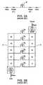
- the driveconsists of six transistors, three high-side and three low-side. All three low-side MOSFETs A LSS , B LSS , and C LSS must have a low resistance connection to the ground pad of the IC.
- a HSS , B HSS , and C HSSmust share a common low-resistance bus to a V DD pad.
- Each phasehas an output pad (A out , B out and C out ) located schematically at the common node between the high-side and low-side MOSFET.
- a out , B out and C outlocated schematically at the common node between the high-side and low-side MOSFET.
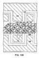
- the output padscannot be located in the center of the die, as shown in Fig. 1B.
- "Deep" bond wires, i.e., bond wires which extend from the edge of the die (where the leadframe is located) to the center of the dieare generally forbidden. The risk of a "deep” bond wire shorting to the surface of the die or to another bond wire is too great.
- FIG. 2Aillustrates an idealized model of a MOSFET M having a bond wire resistance R wire , a lumped metal finger resistance R metal and a MOSFET channel resistance.
- the assumption that the finger resistance can be "lumped"is disproved by reference to Fig. 2B, which shows MOSFETs M A -M F connected in parallel between a drain finger D and a source finger S. Drain finger D contains five squares designated 1d-5d, and source finger S contains five squares designated 1s-5s.
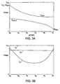
- Fig. 3Aillustrates the voltage drop along source finger S (V source ) and drain finger D (V drain ) when a known current I is forced through the network.
- V sourcesource
- drain finger Ddrain
- the voltage along each fingervaries parabolically as more MOSFETs feed current into the finger.
- V drainsource finger potentials at that point
- V drain - V sourcethe voltage across the MOSFETs (M A and M F ) is a relatively large percentage of the terminal potential (V DD ).
- each MOSFETcan be considered as a linear resistance.
- the current through any given MOSFETis then V ds /R ds , wherein V ds is the voltage across the particular MOSFET and R ds is the resistance of the MOSFET.
- the curve C 1 of Fig. 3Billustrates the voltage V ds across each of MOSFETs M A -M F . It is clear from Fig. 3B that MOSFETs M C and M D at the center of the fingers carry less current than those at the ends. Because they conduct a smaller percentage of the total current, these MOSFETs behave as if they have a higher resistance than the MOSFETs located towards the ends of the fingers. Making a finger even longer adds even more cells to the center that do not carry much current, so the equivalent resistance for a given area of the die increases. As a result, without including any effects due to the gate bias or current saturation of the MOSFETs, the influence of metal finger resistance is to increase the total device resistance nonlinearly with increasing finger length. Fig. 3B also shows the voltage drop that would prevail across each of MOSFETs M A -M F in the ideal model with no parasitic resistance (curve C 3 ) and in the lumped resistance model illustrated in Fig. 2A (curve C 2 ).
- the distributed resistance along finger Sincreases the voltage at the end of the finger (MOSFET M A ) and therefore reduces the level of gate drive.
- a lower gate drive voltage (V gs )means that the MOSFET will have a higher resistance and saturate sooner.
- triangular or wedge-shaped buseshave been used to avoid electromigration (a reliability problem resulting from high current densities in a soft metal such as aluminum). This tends to equalize the voltage drops between the MOSFETs along a given bus or finger (i.e., the cross-sectional area of the bus increases in the direction of the pad), but the restrictions imposed on the layout by triangular buses are incompatible with today's high-density device technology.
- the bus resistance problemis two-dimensional: not only does the metal contribute to resistance along a finger (perpendicular to the die edge), but it also adds a distributed effect in the metal source bus and drain bus along the edge of the die. Any attempt to make triangles out of the bus would result in a waste of area having consequences worse than the distributed resistance problem that it was intended to overcome.
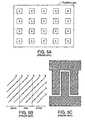
- Fig. 5Aillustrates an array of tightly packed device cells built into a rectilinear grid. some of the advantages of this pattern are discussed in U.S. Patent No. 5,412,239.
- the polysilicon gateis fabricated in a "cookie cutter" geometry, i.e., a sheet with a rectilinear array of openings, the source contacts and drain contacts extending through the openings (labeled S for source, D for drain) in an alternating fashion.
- the traces of the first metal layerare arranged in a diagonal pattern to connect with all contacts of like type (drain or source). Again S designates a source metal trace; D designates a drain metal trace. Then, as shown in Fig.
- the second metal layerincludes interdigitated fingers which are arranged in a pattern parallel to the cells such that alternating fingers are connected through vias to the underlying source and drain cells.
- via connections between the first and second metal layersoccur in alternating "stripes".
- Under a drain stripeonly vias to "drain" first metal buses are included. (This is shown as the central region in Fig. 5B.) Current in first metal layer source buses in this region must flow laterally to the nearest via under a second metal layer source bus.
- the metal strapincludes a relatively thick layer of nickel which is plated electrolessly onto the bus or other conductive path.
- the buscan be formed of an aluminum layer, which might comprise aluminum-silicon or aluminum-copper-silicon. Since the passivation layer does not overlie the metal strap layer, the thickness of the metal strap may be increased to, for example, 20 to 30 ⁇ m without causing cracking in the passivation layer.
- the passivation layeris etched so as to form a longitudinal channel or trench over the bus or other conductive path.
- contact with the busis improved by first depositing or planting an adhesion layer of a metal such as zinc, titanium or platinum.
- the metal strapis then deposited on the thin layer, preferably by electroless plating.
- Another metal layere.g., a gold or silver layer
- Covering the metal strap layer with a thin of metal such as gold or silverallows conventional wire bonding directly to the metal strap at the edge of the die, eliminating the need for special packaging techniques.
- a thick gold layeris substituted for the thick nickel layer. This allows a bond wire to be attached directly to the thick layer.
- the metal strapvirtually eliminates the resistance of the underlying bus or other conductive path, reducing the interconnect sheet resistance by a factor of 5 to 30 as compared with conventional interconnect arrangements.
- a metal strap overlying a bus or fingermay be used to reduce resistance in any IC which includes single or multiple metal layers. This structure is particularly useful, however, in reducing the on-resistance of lateral power devices integrated with logic or control circuitry in power ICs.
- the ICmay include both conventional metal buses covered by a passivation layer as well as buses overlain by a metal strap layer. While the buses which have an overlying metal strap layer may have to be spaced somewhat more widely than is normal, other buses can be conventionally spaced. In this way, high current buses can be mixed with submicron interconnects without comprising tight design rules.
- the fabrication of a metal strap layer on buses which are located at the edge of the diereduces the need for an excessive number of wire bonds to minimize the distributed resistance in these buses.
- Fig. 1Aillustrates a circuit diagram of a conventional three-phase push-pull motor driver.
- Fig. 1Billustrates a possible layout of an IC die which contains the motor driver of Fig. 1A.
- Fig. 1Cillustrates an alternative layout of an IC die which contains the motor driver of Fig. 1A.
- Fig. 2Aillustrates an idealized model of a MOSFET having a bond wire resistance, a lumped metal finger resistance and a channel resistance.
- Fig. 2Billustrates a conventional arrangement of parallel MOSFETs connected between two conductive fingers.
- Fig. 2Cis an equivalent circuit diagram of the arrangement shown in Fig. 2B.
- Fig. 3Ais a graph showing the voltage along the conductive fingers illustrated in Fig. 2B.
- Fig. 3Bis a graph illustrating the voltage across each of the MOSFETs shown in Fig. 2B, as compared with the voltage that would exist under a lumped resistance model and the voltage that would exist absent all parasitic resistances.
- Fig. 4illustrates an interdigitated arrangement of two buses.
- Fig. 5Aillustrates a rectilinear array of MOSFET cells.
- Fig. 5Billustrates the layout of the buses in the first metal layer above the rectilinear array of MOSFET cells.
- Fig. 5Cillustrates the buses in the second metal layer above the rectilinear array of cells.
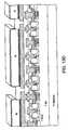
- Fig. 6Aillustrates a top view of a bus arrangement which includes a plurality of interdigitated fingers.
- Fig. 6Billustrates a cross-sectional view of two of the adjacent fingers shown in Fig. 6A.
- Fig. 6Cillustrates an alternative arrangement including a first metal layer and a second metal layer to which a metal strap layer is applied.
- Fig. 7illustrates a cross-sectional view of the use of metal straps in accordance with this invention in a quasi-vertical double-diffused MOSFET device.
- Fig. 8illustrates a top view of the device shown in Fig. 7, illustrating the cross section 7-7 at which Fig. 7 is taken.
- Figs. 9A-9Dillustrate steps in a process which may be used to fabricate a device of the kind illustrated in Figs 7 and 8.
- Fig. 10Aillustrates a cross-sectional view of a closed-cell lateral device including metal straps in accordance with this invention.
- Fig. 10Billustrates a top view of a device similar to that shown in Fig. 10A.
- Figs. 10C-10Eillustrate detailed views of the closed-cell lateral device shown in Figs. 10A and 10B.
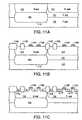
- Figs. 11A-11Dillustrate steps in a process of fabricating a device of the kind shown in Figs. 10A and 10B.
- Fig. 12illustrates a cross-sectional view of a device similar to the devices shown in Figs. 10A and 10B, but having a greater number of cells in each well.
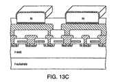
- Fig. 13Aillustrates a conventional NMOS device including a metal strap of the invention.
- Fig. 13Billustrates a device similar to that shown in Fig. 13A except that N-type drift regions have been formed adjacent the N+ regions in each cell of the device.
- Fig. 13Cillustrates a power NMOS device which has a source-body short in each of the source cells.
- Fig. 13Dillustrates a lateral device including a double-diffused P body region and an N-drift region.
- Fig. 13Eillustrates a lateral device equivalent to the quasi-vertical device shown in Fig. 7.
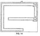
- Fig. 14illustrates a non-power IC having metal straps over the ground and voltage supply (V DD ) buses.
- Fig. 15illustrates a cross-sectional view of a relatively wide, saddle-shaped metal strap.
- Fig. 16illustrates a segmented metal strap.
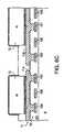
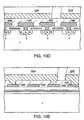
- Fig. 6Aillustrates a top view of a conductive metal layer 60 which is overlain by a metal strap layer 61.
- Metal layer 60includes conductive lines 60A, 60C and 60E, which extend from a bus 60H, and conductive lines 60B, 60D and 60F, which extend from a bus 60G. Lines 60A-60F are arranged in the form of interdigitated fingers. Wires 62 and 63 are bonded to buses 60G and 60H, respectively, at bond locations 62B and 63B.
- Fig. 6Billustrates a cross-sectional view of lines 60D and 60E taken at cross section 6B-6B shown in Fig. 6A.
- Underlying the structureis a silicon substrate 64 over which is formed an oxide layer 65.
- Metal layer 60represented by lines 60D and 60E, is formed on top of oxide layer 65.
- a passivation layer 66overlies oxide layer 65 and covers the edges of lines 60D and 60E.
- Metal strap layer 61includes metal straps 61A and 61D, which overlie lines 60D and 60E, respectively.
- Metal strap layer 61is not covered by passivation layer 66. Rather, passivation layer 66 abuts side edges 61Aa and 61Ab of strap 61A, for example.
- Straps 61A and 61Bare formed in longitudinal channels in passivation layer 66.
- metal strap layer 61includes a nickel laver 67, a thin titanium layer 68 and a thin gold layer 69.
- Titanium layer 68is deposited on top of lines 60D and 60E to improve the adhesion between metal layer 60 and nickel layer 67.
- Gold layer 69is deposited on the top and side surfaces of nickel layer 67 to facilitate wire bonding.
- metal layer 60may be, for example, a second metal layer.
- the underlying first metal layeris not shown.
- Fig. 6Cis a cross-sectional view showing a first metal layer 70 which includes conductive lines 70A-70G.
- Lines 70A-70Gcould be arranged in the manner of the diagonal buses shown in Fig. 5B, for example.
- the lines of the first metal layercould be arranged in an interdigitated comb-like pattern.
- a second metal layer 71includes buses 71A and 71B. Vias connect bus 71A to lines 70A and 70C, and connect bus 71B to lines 70D and 70F.
- a metal strap layer 72is plated on top of buses 71A and 71B.
- Fig. 6Cillustrates how a relatively fine pitch in the lines of the first metal layer can be combined with a larger pitch in the buses of the second metal layer.
- structures according to this inventiondecouple the pitch of the first metal layer lines from the power busing rules entirely.
- the lines of the first metal layerhave no design rules related to the metal straps of the second metal layer.
- a thin second metal layer with tight line-to-line spacingcan be used because the low-resistance is achieved by depositing the thick metal only where the second metal lines are drawn at a wide dimension.
- the processbegins after passivation layer 66 has been formed.
- a thin layer of titaniumis deposited after the passivation layer has been masked and etched.
- the titaniumis then masked and etched into a feature size which is slightly larger than the openings formed in the passivation layer in step 2 above (i.e., the titanium layer slightly overlaps the passivation layer).
- Goldmay be plated on the titanium layer or an intervening layer of nickel may first be deposited. The overlap protects metal layer 60 from damage resulting from later etching or other processing steps.
- Figs. 7 and 8illustrate how a metal strap layer according to this invention may be used to minimize distributed resistance in a power device.
- Fig 7is a view taken at cross-section 7-7 shown in the plan view of Fig. 8.
- Fig. 8shows a drain metal strap 75 which is interdigitated with a source metal strap 78.
- Underlying drain metal strap 75are a second metal bus 76A (hatched lines) and a first metal bus 77A.
- Underlying source metal strap 78are a second metal bus 76B (hatched lines) and a first metal bus 77B.
- the dots in Fig. 8represent vias between the first and second metal layers.
- the structure of the power deviceis shown in Fig. 7.
- Buses 77A and 77Bare part of a first metal layer, and buses 76A and 76B are part of a second metal layer.
- the second metal layer(buses 76A and 76B) is connected to the first metal layer (buses 77A and 77B) through vias in the interlayer dielectric.
- the first metal layerincludes relatively wide buses similar to bus 77B, which connect to the source/body regions of the MOSFET (P body regions 73A-73F) and relatively narrow buses similar to bus 77A, which connect to the drain (N+ sinker 70 and buried layer 71), whereas the pitch of the second metal layer (buses 76A and 76B) is more evenly divided between the source and drain lines.
- a passivation layer 79is deposited on the second metal layer, except for channels down the center of buses 76A and 76B, and then metal straps 75 and 78 are deposited, as described above, including layers of zinc, nickel and gold.
- Figs. 9A-9Dillustrate a sequence of processing steps which yield a device similar to the device illustrated in Figs. 7 and 8.
- a P-type substrate 80is implanted with boron ions at a dose of about 5 x 10 14 cm -2 to form a P+ region where P buried layer 81 is to be located, and with a similar implant of antimony to form an N+ region where N+ buried layer 71 is to be located.
- P substrate 80may have a resistivity of, for example, 4 ohm-cm.
- N-type epitaxial layer 72is grown on the top surface of substrate 80, having a resistivity of from 0.3 to 10 ohm-cm and a thickness of from 2 to 15 ⁇ m.
- the resistivity of N-epitaxial layer 72is around 2 ohm-cm and its thickness is from 5 to 8 ⁇ m.
- a heavily doped P+ sinker and a heavily doped N+ sinkerare then formed and diffused to overlap the up-diffusing P+ and N+ regions, respectively, to form N+ buried layer 71 and N+ sinker 70 as well as a P buried layer 81 and a P isolation region 82.
- a P-type well diffusion and a thick LOCOS field oxidemay be formed to facilitate fabrication of conventional CMOS devices.
- a gate oxidation layer 83is formed and a layer of polysilicon is deposited, doped and etched to form a polysilicon gate 84.
- P-body regions 85A and 85Bare then implanted (for example, at a dose of from 1 to 10 x 10 13 cm -2 boron) and diffused to a depth of from 0.9 to 4 ⁇ m.
- P-body regions 85A and 85Bare self-aligned with gate 84.
- P-body regions 85A and 85Bcan be in the form of individual islands surrounded by gate 84 or in the form of long stripes on either side of gate 84.
- N+ and P+ implantsare introduced through a mask, at dosages of 5 x 10 15 cm -2 and 9 x 10 13 cm -2 , respectively, to form P+ and N+ contact regions.
- Fig. 9Dsurface oxide layers are then masked and etched to form contacts to the N+ drain and the N+/P+ source/body regions.
- Aluminum-copper-silicon(for example, 96%, 2%, 2%) is then sputtered, masked and etched to form buses 77A and 77B.
- viasare opened to buses 77A and 77B, and a second metal layer including buses 76A and 76B is deposited to a thickness from 0.6 to 4 ⁇ m, with a thickness of 0.8 to 1 ⁇ m being preferred.
- Nitride or glass passivation layer 79is then deposited and masked to form channels where metal straps 75 and 78 may be formed.
- Figs. 10A-10Eillustrate how this invention may be applied to a closed-cell lateral device of the kind illustrated in Figs. 5A-5C.
- Fig. 10Aillustrates a modified cross-sectional view of the alternating source and drain cells, with each cell having a lightly doped (N-) region to limit field strength at the P-N junction.
- the cellsare formed in a P epitaxial layer.
- a first metal layerincludes lines 100A-100F, which are arranged diagonally as shown in the broken-away top view of Fig. 10B.
- the second metal layerincludes a drain bus 101A and a source bus 101B.
- the second metal layerincludes other source and drain buses which are interdigitated in the manner shown in Fig. 10B.
- Fig. 10Ais "modified" in that the vias between the buses 101A and 101B and the lines 100A-100F are shown as being in the same cross-sectional plane as the metal contacts from the lines 100A-100F to the individual source and drain regions. As shown in Fig. B, wherein the vias between the buses 101A and 101B and the lines 100A-100F are shaded, this is not the case. This is made even clearer in the detailed top view of Fig. 10C, and in the detailed cross-section views shown in Figs. 10D and 10E, which are taken at cross sections 10D-10D and 10E-10E, respectively, shown in Fig. 10C.
- buses 101A and 101BIn contact with the top surface of buses 101A and 101B are metal straps 102A and 102B in accordance with this invention. With this arrangement, the resistance between any point on buses 102A and 102B and any other point on the same bus (e.g., a bonding wire connection) is very low.
- Figs. 11A-11Dillustrate the fabrication of two devices of the kind shown in Figs. 10A and 10B, one device being an N-channel device and the other device being a P-channel device.
- the P-channel deviceis fabricated within an N-well region while the N-channel device is fabricated within a P-epitaxial layer in which a P-well may optionally be included.
- the processbegins with a P-type substrate 110 (resistivity 2 to 20 ohm-cm) in which N-type dopant is implanted at a dosage of 1 to 5 x 10 15 cm -2 .
- a P-type epitaxial layer 111is then grown on the top surface of P substrate 110, and by diffusion an N buried layer 112 is formed at the junction between P substrate 110 and P epitaxial layer 111.
- N-type dopantis then implanted in the top surface of P epitaxial layer 111 to form an N well 113 for the P-channel device.
- a P well 114may be formed similarly by implanting P-type dopant.
- the resulting structureis shown in Fig. 11A for the N-channel device.
- LOCOS oxide regions 115A-115Dare formed at the top surface of P epitaxial layer 111.
- a gate oxide layerfrom 100 to 2000 ⁇ thick (preferably 175 to 400 ⁇ thick) is grown.
- a polysilicon layeris deposited, doped and etched to form gates 116A-116D.
- N well 113 and P well 114are implanted in N well 113 and P well 114, respectively.
- the P+ regions in N well 113are self aligned with gates 116A and 116B and form the source and drain diffusions for the power PMOS device.
- a photoresist maskis used to hold the N+ regions 1 to 2 ⁇ m back from gates 116C and 116D, and a blanket N- drift implant forms a lightly doped drain (LDD) arrangement, the composite structure of the N+ and N- regions forming the source and drain diffusions of the power NMOS device.
- LDDlightly doped drain
- the N+ regionmay abut the polysilicon gate thereby eliminating the drift (N-) region.
- the N-drift implantcan precede formation of an oxide sidewall spacer on the polysilicon gate.
- the N+ implantationis then held away from the gate by the sidewall oxide, forming a 0.25 ⁇ m drift length on both the source and drain.
- An N+ contact region 117Ais formed in N well 113 and a P+ contact region 117B is formed in P well 114.
- Fig. 11Dshows a first metal layer including diagonal buses 118A-118F, each of which is connected through a via to one of the P+ or drifted N+ regions.
- An additional diagonal bus 118Gis connected to the N+ contact region in N well 113, and an additional diagonal bus 118H is connected to the P+ contact region in P well 114.
- the second metal layerincludes buses 119A and 119B, which are interdigitated as shown in Fig. 10B. If the full extent of the PMOS and NMOS devices were shown, a second bus in the second metal layer would be shown connected to line 118B in the PMOS device; similarly, a second bus in the second metal layer would be shown connected to line 118E in the NMOS device. Metal straps (not shown in Fig. 11D) are then plated on the top surface of buses 119A and 119B.
- Fig. 12illustrates a cross-sectional view of a similar complementary pair of devices, having a greater number of cells in each well, showing metal straps 120A-120D plated on the top of buses 121A-121D, respectively.
- Figs. 13A-13Eillustrate other devices to which the principles of this invention may be applied.
- Fig. 13Ashows a conventional NMOS device constructed in a P well.
- the device shown in Fig. 13Bis similar, but sidewall spacers have been used to form short (e.g., 0.2 ⁇ m) lightly doped N-type drift regions adjacent the N+ regions.
- the formation and purpose of lightly doped drains (LDDs)are described in Wolf, Silicon Processing For The VLSI Era , Vol. 2, Lattice Press (1990), pp. 354-360.
- Fig. 13Cillustrates a power NMOS device which has a N+/P+ source/body short in each of the source cells.
- Fig. 13Ashows a conventional NMOS device constructed in a P well.
- the device shown in Fig. 13Bis similar, but sidewall spacers have been used to form short (e.g., 0.2 ⁇ m) lightly doped N-type drift regions adjacent the
- FIG. 13Dillustrates a lateral device formed in a P-type epitaxial layer, where the double-diffused P body region is used to prevent channel punchthrough and an implanted N-drift region is optimized for some voltage, e.g., 60 V.
- Fig. 13Eis the lateral equivalent of the quasi-vertical device shown in Fig. 7.
- the metal strap layeris made too wide, it may tend to form in a "saddle" shape, as shown in Fig. 15, because the electroplating solution near the center of the strap tends to become depleted of metal ions.
- This problemcan be alleviated by limiting the width of the strap to about 25 ⁇ m or less.
- the strapcan be formed in longitudinal segments, as shown in the top view of Fig. 16, which allows the metal ions to gain access to the central portion of the strap through the "joints" between the segments. While the resistance of the bus increases slightly if this technique is used, the overall distributed resistance is still much less than it would be absent a metal strap layer.
- segmenting the metal straphas the added benefit of reducing stress due to dissimilar temperature coefficients of expansion between the thick metal and the underlying silicon.
- the technique of this inventionis applicable to other types of lateral power devices. Moreover, the technique is not limited to power devices.
- the main bus in an ICmay also benefit from a low distributed resistance.
- the ground bus 140may have over 30 squares of resistance associated with it. For a 1 ⁇ m thick second metal layer with 30 ⁇ /sq., this resistance amounts to nearly 1 ohm. Using a 30 ⁇ m thick nickel and 1 ⁇ m gold plated bus, this resistance falls to around 1.8 m ⁇ /sq. or a total resistance of only 60 ⁇ m ⁇ .
- the reduced resistanceimproves efficiency, reduces the risk of CMOS latch-up, reduces "ground bounce” (i.e., a change in the voltage along the length of a ground bus line as current in the bus line changes during normal operation) and improves the switching waveforms of high current buffer outputs.
- ground bouncei.e., a change in the voltage along the length of a ground bus line as current in the bus line changes during normal operation
- the use of a thick single or multiple layer sandwich of metal, after the passivation layer is formed, to substantially eliminate the resistance of thin metal buses in a lateral power deviceis not limited to any particular formation process, and it includes any deposition or electroless or electroplating process.
Landscapes
- Engineering & Computer Science (AREA)
- Computer Hardware Design (AREA)
- Microelectronics & Electronic Packaging (AREA)
- Power Engineering (AREA)
- Physics & Mathematics (AREA)
- Condensed Matter Physics & Semiconductors (AREA)
- General Physics & Mathematics (AREA)
- Manufacturing & Machinery (AREA)
- Insulated Gate Type Field-Effect Transistor (AREA)
- Internal Circuitry In Semiconductor Integrated Circuit Devices (AREA)
- Metal-Oxide And Bipolar Metal-Oxide Semiconductor Integrated Circuits (AREA)
- Semiconductor Integrated Circuits (AREA)
Description
- This application is related to Applicant's copendingand simultaneously filed European application which claimspriority from US Application Ser. No. 08/367,486, filed onDecember 30 1994.
- This invention relates to lateral power MOSFETsfabricated in the form of an integrated circuit and, inparticular, to an integrated circuit which has reducedresistances in internal buses and other conduction pathslinking the MOSFETs and other components to each other andto external devices.
- The total resistance of a power MOSFET when it isturned on is generally the sum of the resistance of themetal conductors (bonding wires, buses, etc.) And thechannel resistance. The performance of power MOSFETsfabricated as integrated circuits (ICS) has suffered incomparison with the performance of their discretecounterparts because of the resistance of the metalconductors. This problem was overcome temporarily by theintroduction of dual-layer metallisation into power ICs.More recently, however, further reductions in the channelresistance of vertical and lateral power MOSFETs have onceagain focused attention on the resistance of the metalinterconnects. In some cases, for example, where cross-chipbusing is required, the metal resistance can exceed theresistance of the silicon devices.
- In a conventional IC power MOSFET, the metallayers are deposited by sputtering, chemical vapordeposition, or evaporation and are overlain by apassivation layer which is typically formed of siliconnitride or some type of glass (e.g.,borophosphosilicate glass). Increasing the thicknessof metal layers so fabricated to minimize theircontribution to resistance is in many ways incompatiblewith the desire for increased packing density withinthe IC. Moreover, even at a thickness of 1 µm, a sheetresistance of 30 mΩ/square can present a significantproblem in the design of a 50 mΩ lateral power MOSFET.As operating voltages decline from 12 V to 5 V, andeven to 3 V, the size of the individual device cellshas been reduced. In a closed-cell array ofalternating source and drain cells, for example, whichis currently the preferred structure, reducing the sizeof the cells forces the first metal layer to a tighterpitch and smaller contacts. In some embodiments, thispitch requirement reduces the thickness of the firstmetal layer to 1 µm or below, even as low as 0.3 µm.Moreover, a thick first metal layer may complicate theplanarization process needed to avoid step coverageproblems in the second metal layer.
- Increasing the thickness of the second metal layeralso presents problems, particularly in the etchingprocess. Beyond a thickness of 2 µm, dry etchingbecomes difficult due to the need for a thickphotoresist and due to complexities in the metal etchprocess itself (i.e., redeposition of etched materials,changes in gas stoichiometry, heating, etc.). Wetetching suffers from lift off of the resist, whichleads to notching ("mouse biting") and requires verylarge metal-to-metal spacing (for example, 15 µm for a4 µm thick metal layer) and a large metal overlap ofvias. A metal layer meeting these requirements is useless in the logic areas of the IC, because theminimum line widths and spacing permitted yield toolarge a pitch and too few interconnects per unit areato allow for dense packing of logic.
- Metal resistance impacts two areas of power ICdesign in particular: (i) the buses between devices andalong the edge of the die, and (ii) the conductivefingers within a given lateral power device. In thebuses between devices the metal acts as a seriesresistance element. Its contribution to totalresistance can be calculated by the number of squarestimes its sheet resistance. Consider, for example, thethree-phase push-pull motor driver shown in Fig. 1A.The drive consists of six transistors, three high-sideand three low-side. All three low-side MOSFETs ALSS,BLSS, and CLSS must have a low resistance connection tothe ground pad of the IC. Likewise, all three high-sidedevices, AHSS, BHSS, and CHSS must share a common low-resistancebus to a VDD pad. Each phase has an outputpad (Aout, Bout and Cout) located schematically at thecommon node between the high-side and low-side MOSFET.Thus, at least five power pads are required.Unfortunately, the output pads cannot be located in thecenter of the die, as shown in Fig. 1B. "Deep" bondwires, i.e., bond wires which extend from the edge ofthe die (where the leadframe is located) to the centerof the die are generally forbidden. The risk of a"deep" bond wire shorting to the surface of the die orto another bond wire is too great. Another risk issagging of the wire where it touches the "scribestreet" causing a short to ground (a failure referredto as "wire wash"). In thin profile surface-mountpackages, a deep bond wire may even protrude throughthe top of the plastic package. Moreover, a singlebond wire may exhibit a resistance of over 50 mΩ. Forthese and other reasons, the bond pads in an IC must generally be located near the edge of the die.
- Continuing the example, rearranging the push-pullstages to place the output pads near the edge of thedie, as shown in Fig. 1C, further lengthens the groundand VDD bus lines, thereby increasing their resistance.The net result is that no layout satisfies the need forlow-resistance VDD, ground and output connectionswithout increasing the number of power-related padsfrom five to at least seven.
- The resistive contributions of the metal within adevice are even more complex. Fig. 2A illustrates anidealized model of a MOSFET M having a bond wireresistance Rwire, a lumped metal finger resistance Rmetaland a MOSFET channel resistance. The assumption thatthe finger resistance can be "lumped" is disproved byreference to Fig. 2B, which shows MOSFETs MA-MFconnected in parallel between a drain finger D and asource finger S. Drain finger D contains five squaresdesignated 1d-5d, and source finger S contains fivesquares designated 1s-5s.
- Assume for the moment that MOSFETs MA-MF all carrythe same current. Notice that, on the source side, themetal square labeled 5s must conduct the current of allsix MOSFETs.
Square 5d on the drain side carries onlythe current of MOSFET MF. Instead, the square labeled1d must handle all of the current. Since more currentis flowing insquare 1d on the drain side and square 5son the source side, the voltage drop in these squaresis higher than in the other squares. The equivalentcircuit is shown in Fig. 2C, wherein the distributedresistances represented bysquares 1d-5d and 1s-5s areshown between the individual MOSFETs. Because of thisdistributed resistance, the MOSFETs cannot beconsidered in parallel nor can the current through thembe considered uniform. The net result is that theequivalent resistance of the network can be higher than the model of the simple lumped resistance of the metalfinger added to the parallel resistances of theMOSFETs. - Fig. 3A illustrates the voltage drop along sourcefinger S (Vsource) and drain finger D (Vdrain) when a knowncurrent I is forced through the network. As expected,most of the voltage drop occurs at one end of sourcefinger S and at the other end of the drain finger D.The voltage along each finger varies parabolically asmore MOSFETs feed current into the finger. Given thenonlinear variation of Vsource and Vdrain, the voltage acrossany given MOSFET is the difference between the drainand source finger potentials at that point (Vdrain -Vsource). Note that, at the two ends, the voltage acrossthe MOSFETs (MA and MF) is a relatively large percentageof the terminal potential (VDD). Halfway down thefingers, however, the voltage drops along each fingerbecome significant, and the voltage across the centralMOSFETs (MC and MD) falls to a minimum. If we assumethat the current density is low enough to preventsaturation in any MOSFET, then each MOSFET can beconsidered as a linear resistance. The current throughany given MOSFET is then Vds/Rds, wherein Vds is thevoltage across the particular MOSFET and Rds is theresistance of the MOSFET.
- The curve C1 of Fig. 3B illustrates the voltage Vdsacross each of MOSFETs MA-MF. It is clear from Fig. 3Bthat MOSFETs MC and MD at the center of the fingerscarry less current than those at the ends. Becausethey conduct a smaller percentage of the total current,these MOSFETs behave as if they have a higherresistance than the MOSFETs located towards the ends ofthe fingers. Making a finger even longer adds evenmore cells to the center that do not carry muchcurrent, so the equivalent resistance for a given areaof the die increases. As a result, without including any effects due to the gate bias or current saturationof the MOSFETs, the influence of metal fingerresistance is to increase the total device resistancenonlinearly with increasing finger length. Fig. 3Balso shows the voltage drop that would prevail acrosseach of MOSFETs MA-MF in the ideal model with noparasitic resistance (curve C3) and in the lumpedresistance model illustrated in Fig. 2A (curve C2).
- As the voltage between the gate and source pads isincreased by external circuit conditions, the devicesat the ends of the fingers go into current saturationfirst, placing an increased conduction burden on thecells along the center of the fingers. The lattercells then go into saturation sooner than they wouldotherwise, and the effect cascades. This phenomenonpoints up the second problem with finger resistance,i.e., the non-uniform current leads to prematuresaturation of the individual MOSFETs, a smaller regionof linear operation, and a non-uniform distribution ofpower along the metal fingers S and D.
- In addition, the distributed resistance alongfinger S increases the voltage at the end of the finger(MOSFET MA) and therefore reduces the level of gatedrive. The farther away the device is from the gatepad, the larger the reduction on gate drive. A lowergate drive voltage (Vgs) means that the MOSFET will havea higher resistance and saturate sooner.
- In the prior art, triangular or wedge-shaped buseshave been used to avoid electromigration (a reliabilityproblem resulting from high current densities in a softmetal such as aluminum). This tends to equalize thevoltage drops between the MOSFETs along a given bus orfinger (i.e., the cross-sectional area of the busincreases in the direction of the pad), but therestrictions imposed on the layout by triangular busesare incompatible with today's high-density device technology. Moreover, as the interdigitated busarrangement shown in Fig. 4 indicates, the busresistance problem is two-dimensional: not only doesthe metal contribute to resistance along a finger(perpendicular to the die edge), but it also adds adistributed effect in the metal source bus and drainbus along the edge of the die. Any attempt to maketriangles out of the bus would result in a waste ofarea having consequences worse than the distributedresistance problem that it was intended to overcome.
- Fig. 5A illustrates an array of tightly packeddevice cells built into a rectilinear grid. some ofthe advantages of this pattern are discussed in U.S.Patent No. 5,412,239.The polysilicon gate is fabricated in a "cookie cutter"geometry, i.e., a sheet with a rectilinear array ofopenings, the source contacts and drain contactsextending through the openings (labeled S for source, Dfor drain) in an alternating fashion. As shown in Fig.5B, the traces of the first metal layer are arranged ina diagonal pattern to connect with all contacts of liketype (drain or source). Again S designates a sourcemetal trace; D designates a drain metal trace. Then,as shown in Fig. 5C, the second metal layer includesinterdigitated fingers which are arranged in a patternparallel to the cells such that alternating fingers areconnected through vias to the underlying source anddrain cells. In other words, via connections betweenthe first and second metal layers occur in alternating"stripes". Under a drain stripe, only vias to "drain"first metal buses are included. (This is shown as thecentral region in Fig. 5B.) Current in first metallayer source buses in this region must flow laterallyto the nearest via under a second metal layer sourcebus.
- What is needed, then, is a means to conduct high currents in an IC power device at low values of laterallydistributed resistance. The technique should place minimumrestrictions on the geometric patterns of the polysilicongate and first metal layer so as to allow them to beoptimized for achieving the minimum device resistance in agiven area. Furthermore, extremely thick passivated metalmust be avoided to prevent cracking of the passivant overmetal steps. Such cracks may create reliability problems.
- In accordance with this invention there is provided alateral integrated circuit die according to
claim 1. - In a preferred embodiment, the metal strap includes a relatively thick layer of nickel which is plated electrolessly onto the bus or other conductive path. The bus can be formed of an aluminum layer, which might comprisealuminum-silicon or aluminum-copper-silicon. Since thepassivation layer does not overlie the metal strap layer,the thickness of the metal strap may be increased to, forexample, 20 to 30 µm without causing cracking in thepassivation layer.
- In a method of fabricating this arrangement, thepassivation layer is etched so as to form a longitudinalchannel or trench over the bus or other conductive path. Ina preferred method, contact with the bus is improved byfirst depositing or planting an adhesion layer of a metalsuch as zinc, titanium or platinum. The metal strap is thendeposited on the thin layer, preferably by electrolessplating. Another metal layer (e.g., a gold or silver layer)can be deposited on the top surface of the metal strap.Covering the metal strap layer with a thin of metalsuch as gold or silver allows conventional wire bondingdirectly to the metal strap at the edge of the die,eliminating the need for special packaging techniques.
- In another embodiment, a thick gold layer issubstituted for the thick nickel layer. This allows abond wire to be attached directly to the thick layer.
- The metal strap virtually eliminates theresistance of the underlying bus or other conductivepath, reducing the interconnect sheet resistance by afactor of 5 to 30 as compared with conventionalinterconnect arrangements. The need for "deep" bonds,i.e., long wire bonds extending into the interior ofthe die, is also eliminated.
- A metal strap overlying a bus or finger maybe used to reduce resistance in any IC which includessingle or multiple metal layers. This structure isparticularly useful, however, in reducing the on-resistanceof lateral power devices integrated withlogic or control circuitry in power ICs. The IC mayinclude both conventional metal buses covered by apassivation layer as well as buses overlain by a metalstrap layer. While the buses which have an overlyingmetal strap layer may have to be spaced somewhat morewidely than is normal, other buses can beconventionally spaced. In this way, high current busescan be mixed with submicron interconnects withoutcomprising tight design rules. The fabrication of ametal strap layer on buses which are located at theedge of the die reduces the need for an excessivenumber of wire bonds to minimize the distributedresistance in these buses.
- Fig. 1A illustrates a circuit diagram of aconventional three-phase push-pull motor driver.
- Fig. 1B illustrates a possible layout of an IC diewhich contains the motor driver of Fig. 1A.
- Fig. 1C illustrates an alternative layout of an ICdie which contains the motor driver of Fig. 1A.
- Fig. 2A illustrates an idealized model of a MOSFEThaving a bond wire resistance, a lumped metal fingerresistance and a channel resistance.
- Fig. 2B illustrates a conventional arrangement ofparallel MOSFETs connected between two conductivefingers.
- Fig. 2C is an equivalent circuit diagram of thearrangement shown in Fig. 2B.
- Fig. 3A is a graph showing the voltage along theconductive fingers illustrated in Fig. 2B.
- Fig. 3B is a graph illustrating the voltage acrosseach of the MOSFETs shown in Fig. 2B, as compared withthe voltage that would exist under a lumped resistancemodel and the voltage that would exist absent allparasitic resistances.
- Fig. 4 illustrates an interdigitated arrangementof two buses.
- Fig. 5A illustrates a rectilinear array of MOSFETcells.
- Fig. 5B illustrates the layout of the buses in thefirst metal layer above the rectilinear array of MOSFETcells.
- Fig. 5C illustrates the buses in the second metallayer above the rectilinear array of cells.
- Fig. 6A illustrates a top view of a busarrangement which includes a plurality ofinterdigitated fingers.
- Fig. 6B illustrates a cross-sectional view of twoof the adjacent fingers shown in Fig. 6A.
- Fig. 6C illustrates an alternative arrangement including a first metal layer and a second metal layerto which a metal strap layer is applied.
- Fig. 7 illustrates a cross-sectional view of theuse of metal straps in accordance with this inventionin a quasi-vertical double-diffused MOSFET device.
- Fig. 8 illustrates a top view of the device shownin Fig. 7, illustrating the cross section 7-7 at whichFig. 7 is taken.
- Figs. 9A-9D illustrate steps in a process whichmay be used to fabricate a device of the kindillustrated in Figs 7 and 8.
- Fig. 10A illustrates a cross-sectional view of aclosed-cell lateral device including metal straps inaccordance with this invention.
- Fig. 10B illustrates a top view of a devicesimilar to that shown in Fig. 10A.
- Figs. 10C-10E illustrate detailed views of theclosed-cell lateral device shown in Figs. 10A and 10B.
- Figs. 11A-11D illustrate steps in a process offabricating a device of the kind shown in Figs. 10A and10B.
- Fig. 12 illustrates a cross-sectional view of adevice similar to the devices shown in Figs. 10A and10B, but having a greater number of cells in each well.
- Fig. 13A illustrates a conventional NMOS deviceincluding a metal strap of the invention.
- Fig. 13B illustrates a device similar to thatshown in Fig. 13A except that N-type drift regions havebeen formed adjacent the N+ regions in each cell of thedevice.
- Fig. 13C illustrates a power NMOS device which hasa source-body short in each of the source cells.
- Fig. 13D illustrates a lateral device including adouble-diffused P body region and an N-drift region.
- Fig. 13E illustrates a lateral device equivalentto the quasi-vertical device shown in Fig. 7.
- Fig. 14 illustrates a non-power IC having metalstraps over the ground and voltage supply (VDD) buses.
- Fig. 15 illustrates a cross-sectional view of arelatively wide, saddle-shaped metal strap.
- Fig. 16 illustrates a segmented metal strap.
- Fig. 6A illustrates a top view of a
conductivemetal layer 60 which is overlain by ametal strap layer 61.Metal layer 60 includesconductive lines bus 60H, andconductivelines bus 60G.Lines 60A-60F are arranged in the form ofinterdigitated fingers.Wires buses bond locations - Fig. 6B illustrates a cross-sectional view of
lines cross section 6B-6B shown inFig. 6A. Underlying the structure is asiliconsubstrate 64 over which is formed anoxide layer 65.Metal layer 60, represented bylines oxide layer 65. Apassivation layer 66 overliesoxide layer 65 and covers the edges oflines Metal strap layer 61 includesmetalstraps 61A and 61D, which overlielines Metal strap layer 61 is not covered bypassivation layer 66. Rather,passivation layer 66abuts side edges 61Aa and 61Ab ofstrap 61A, forexample.Straps passivation layer 66. In this embodiment,metal strap layer 61 includes anickel laver 67, athintitanium layer 68 and athin gold layer 69.Titanium layer 68is deposited on top oflines metal layer 60 andnickel layer 67.Gold layer 69 is deposited on the top and side surfacesofnickel layer 67 to facilitate wire bonding. - In Figs. 6A and 6B,
metal layer 60 may be, forexample, a second metal layer. The underlying firstmetal layer is not shown. - Fig. 6C is a cross-sectional view showing a
firstmetal layer 70 which includesconductive lines 70A-70G.Lines 70A-70G could be arranged in the manner of thediagonal buses shown in Fig. 5B, for example.Alternatively, the lines of the first metal layer couldbe arranged in an interdigitated comb-like pattern. Asecond metal layer 71 includesbuses bus 71A tolines bus 71B tolines metal strap layer 72 isplated on top ofbuses - The following is a description of a process forforming
metal strap layer 61. The process begins afterpassivation layer 66 has been formed. - 1. The same mask that is used to form the padopenings in
passivation layer 66 is used to define thelocations ofmetal straps lines - 2.
Passivation layer 66 is etched with a wetchemical or dry etchant to form longitudinal channelsoverlines - 3. The exposed surfaces of
lines - 4. A zincate solution is used to electrolesslyplate a thin layer of zinc, and the zinc layer isetched back with sulfuric acid. This step may berepeated several times to form a smooth, uniform zinclayer. The result is
zinc layer 68, which ispreferably a monolayer. - 5.
Nickel layer 67 is plated electrolessly,using a hypophosphate nickel solution, to a targetthickness (e.g., 12-25 µm). - 6. The exposed surface of
nickel layer 67 isrinsed with water. - 7. The wafer is immersed in a gold solution toplate a thin gold layer 0.1 to 0.3 µm thick on
nickellayer 67. - 8. The gold layer is cleaned with hydrochloricacid.
- 9. Gold is plated on thin gold layerelectrolessly using an autocatalytic cyanide /goldsolution. The result is
gold layer 69. - 10. A final water rinse is performed. After dieattach, wires are bonded to the exposed gold,preferably near the edge of the die. Gold or aluminumwires may be used.
- Further information on this process is containedin Lawrence Durani,Engineering Handbook, 4th Ed., pg.438.
- In an alternative process, a thin layer oftitanium is deposited after the passivation layer hasbeen masked and etched. The titanium is then maskedand etched into a feature size which is slightly largerthan the openings formed in the passivation layer in
step 2 above (i.e., the titanium layer slightlyoverlaps the passivation layer). Gold may be plated onthe titanium layer or an intervening layer of nickelmay first be deposited. The overlap protectsmetallayer 60 from damage resulting from later etching orother processing steps. - Figs. 7 and 8 illustrate how a metal strap layeraccording to this invention may be used to minimizedistributed resistance in a power device. Fig7 is a view taken at cross-section 7-7 shown in theplan view of Fig. 8. Fig. 8 shows a
drain metal strap 75 which is interdigitated with asource metal strap 78. Underlyingdrain metal strap 75 are asecond metalbus 76A (hatched lines) and afirst metal bus 77A.Underlyingsource metal strap 78 are asecond metal bus 76B (hatched lines) and afirst metal bus 77B. Thedots in Fig. 8 represent vias between the first andsecond metal layers. - The structure of the power device is shownin Fig. 7. Current flows from
drain metal strap 75throughbuses N+ sinker 70, an N+buriedlayer 71, anN epitaxial region 72, and thenthrough channel regions in each ofP body regions 73A-73F.Conduction in the channel regions is controlledby gate 74A-74D. Current leaves the channel regions inP body regions 73A-73F and flows through N+ regions(not numbered) andbuses metalstrap 78, which is in contact withbus 76B.Buses buses - The second metal layer (
buses buses bus 77B, which connect to the source/body regions ofthe MOSFET (P body regions 73A-73F) and relativelynarrow buses similar tobus 77A, which connect to thedrain (N+ sinker 70 and buried layer 71), whereas thepitch of the second metal layer (buses passivation layer 79 is deposited on the second metallayer, except for channels down the center ofbuses - Figs. 9A-9D illustrate a sequence of processingsteps which yield a device similar to the deviceillustrated in Figs. 7 and 8. As shown in Fig. 9A, aP-
type substrate 80 is implanted with boron ions at adose of about 5 x 1014 cm-2 to form a P+ region where Pburiedlayer 81 is to be located, and with a similarimplant of antimony to form an N+ region where N+buriedlayer 71 is to be located.P substrate 80 mayhave a resistivity of, for example, 4 ohm-cm. N-typeepitaxial layer 72 is grown on the top surface ofsubstrate 80, having a resistivity of from 0.3 to 10ohm-cm and a thickness of from 2 to 15 µm. Preferably,the resistivity of N-epitaxial layer 72 is around 2ohm-cm and its thickness is from 5 to 8 µm. A heavilydoped P+ sinker and a heavily doped N+ sinker are thenformed and diffused to overlap the up-diffusing P+ andN+ regions, respectively, to form N+ buriedlayer 71andN+ sinker 70 as well as a P buriedlayer 81 and aPisolation region 82. In other areas (not shown) aP-type well diffusion and a thick LOCOS field oxide may be formed to facilitate fabrication of conventionalCMOS devices. - As shown in Fig. 9B, a
gate oxidation layer 83 isformed and a layer of polysilicon is deposited, dopedand etched to form apolysilicon gate 84. P-bodyregions body regions gate 84. P-body regions gate 84 or in the form of long stripes oneither side ofgate 84. - Next, as shown in Fig. 9C, N+ and P+ implants areintroduced through a mask, at dosages of 5 x 1015 cm-2and 9 x 1013 cm-2, respectively, to form P+ and N+contact regions.
- As shown in Fig. 9D, surface oxide layers are thenmasked and etched to form contacts to the N+ drain andthe N+/P+ source/body regions. Aluminum-copper-silicon(for example, 96%, 2%, 2%) is then sputtered, maskedand etched to form
buses buses layerincluding buses glass passivation layer 79 isthen deposited and masked to form channels where metalstraps 75 and 78 may be formed. - Figs. 10A-10E illustrate how this invention may beapplied to a closed-cell lateral device of the kindillustrated in Figs. 5A-5C. Fig. 10A illustrates amodified cross-sectional view of the alternating sourceand drain cells, with each cell having a lightly doped(N-) region to limit field strength at the P-Njunction. The cells are formed in a P epitaxial layer. A first metal layer includes
lines 100A-100F, which arearranged diagonally as shown in the broken-away topview of Fig. 10B. The second metal layer includes adrain bus 101A and asource bus 101B. The second metallayer includes other source and drain buses which areinterdigitated in the manner shown in Fig. 10B. - Fig. 10A is "modified" in that the vias betweenthe
buses lines 100A-100F areshown as being in the same cross-sectional plane as themetal contacts from thelines 100A-100F to theindividual source and drain regions. As shown in Fig.B, wherein the vias between thebuses lines 100A-100F are shaded, this is not the case.This is made even clearer in the detailed top view ofFig. 10C, and in the detailed cross-section views shownin Figs. 10D and 10E, which are taken atcross sections 10D-10D and 10E-10E, respectively, shown in Fig. 10C. - In contact with the top surface of
buses metal straps buses - Figs. 11A-11D illustrate the fabrication of twodevices of the kind shown in Figs. 10A and 10B, onedevice being an N-channel device and the other devicebeing a P-channel device. In the cross-sectional viewsof Figs. 10A and 10B, the P-channel device isfabricated within an N-well region while the N-channeldevice is fabricated within a P-epitaxial layer inwhich a P-well may optionally be included.
- The process begins with a P-type substrate 110(
resistivity 2 to 20 ohm-cm) in which N-type dopant isimplanted at a dosage of 1 to 5 x 1015 cm-2. A P-typeepitaxial layer 111 is then grown on the top surface ofP substrate 110, and by diffusion an N buriedlayer 112 is formed at the junction betweenP substrate 110 andPepitaxial layer 111. N-type dopant is then implantedin the top surface ofP epitaxial layer 111 to form anN well 113 for the P-channel device. A P well 114 maybe formed similarly by implanting P-type dopant. Theresulting structure is shown in Fig. 11A for the N-channeldevice. - As shown in Fig. 11B,
LOCOS oxide regions 115A-115Dare formed at the top surface ofP epitaxial layer 111. Next, a gate oxide layer from 100 to 2000 Å thick(preferably 175 to 400 Å thick) is grown. Apolysilicon layer is deposited, doped and etched toformgates 116A-116D. - As shown in Fig. 11C, P+ regions and N+ regionsare implanted in N well 113 and P well 114,respectively. The P+ regions in N well 113 are selfaligned with
gates N+regions 1 to 2 µm back fromgates N+ contact region 117A is formed in N well113 and aP+ contact region 117B is formed in P well114. - Fig. 11D shows a first metal layer including
diagonal buses 118A-118F, each of which is connectedthrough a via to one of the P+ or drifted N+ regions. An additionaldiagonal bus 118G is connected to the N+contact region in N well 113, and an additionaldiagonal bus 118H is connected to the P+ contact regionin P well 114. - The second metal layer includes
buses buses - Fig. 12 illustrates a cross-sectional view of asimilar complementary pair of devices, having a greaternumber of cells in each well, showing
metal straps 120A-120D plated on the top ofbuses 121A-121D,respectively. - Figs. 13A-13E illustrate other devices to whichthe principles of this invention may be applied. Fig.13A shows a conventional NMOS device constructed in a Pwell. The device shown in Fig. 13B is similar, butsidewall spacers have been used to form short (e.g.,0.2 µm) lightly doped N-type drift regions adjacent theN+ regions. The formation and purpose of lightly dopeddrains (LDDs) are described in Wolf,Silicon ProcessingFor The VLSI Era, Vol. 2, Lattice Press (1990), pp.354-360. Fig. 13Cillustrates a power NMOS device which has a N+/P+source/body short in each of the source cells. Fig.13D illustrates a lateral device formed in a P-typeepitaxial layer, where the double-diffused P bodyregion is used to prevent channel punchthrough and animplanted N-drift region is optimized for some voltage,e.g., 60 V. Finally, Fig. 13E is the lateralequivalent of the quasi-vertical device shown in Fig. 7.
- If the metal strap layer is made too wide, it maytend to form in a "saddle" shape, as shown in Fig. 15,because the electroplating solution near the center ofthe strap tends to become depleted of metal ions. Thisproblem can be alleviated by limiting the width of thestrap to about 25 µm or less. Alternatively, the strapcan be formed in longitudinal segments, as shown in thetop view of Fig. 16, which allows the metal ions togain access to the central portion of the strap throughthe "joints" between the segments. While theresistance of the bus increases slightly if thistechnique is used, the overall distributed resistanceis still much less than it would be absent a metalstrap layer. Moreover, segmenting the metal strap hasthe added benefit of reducing stress due to dissimilartemperature coefficients of expansion between the thickmetal and the underlying silicon.
- The technique of this invention, using a metalstrap layer and conventional wire bonds, is applicableto other types of lateral power devices. Moreover, thetechnique is not limited to power devices. The mainbus in an IC may also benefit from a low distributedresistance. For example, in the IC shown in Fig. 14,the
ground bus 140 may have over 30 squares ofresistance associated with it. For a 1 µm thick secondmetal layer with 30 Ω/sq., this resistance amounts tonearly 1 ohm. Using a 30 µm thick nickel and 1 µm goldplated bus, this resistance falls to around 1.8 mΩ/sq.or a total resistance of only 60 µm Ω. The reducedresistance improves efficiency, reduces the risk ofCMOS latch-up, reduces "ground bounce" (i.e., a changein the voltage along the length of a ground bus line ascurrent in the bus line changes during normaloperation) and improves the switching waveforms of highcurrent buffer outputs. - Theuse of a thick single or multiple layer sandwich ofmetal, after the passivation layer is formed, tosubstantially eliminate the resistance of thin metalbuses in a lateral power device is notlimited to any particular formation process, and itincludes any deposition orelectroless or electroplating process.
Claims (36)
- A lateral integrated circuit die comprising:a substrate (64) comprising a semiconductormaterial, said substrate (64) having a top surface;a conductive line (60D, 71A, 76B) above said topsurface and having a length extending generallyparallel to said top surface;a metal strap (61A, 72, 78) formed on a surface ofsaid conductive line (60D, 71A, 76B), said metal strap(61A, 72, 78) having a length extending generallyparallel to said top surface, and covering saidconductive line (60D, 71A, 76B)said conductive line (60D, 71A, 76B) and saidmetal strap (61A, 72, 78) being for conducting acurrent flow primarily in a direction parallel to saidtop surface of said substrate (64); anda passivation layer (66, 79) forming a portion ofa top surface of said die, said die beingcharacterisedin that said metal strap covers said conductive line along itswhole extension and without covering areas of thesurrounding structure and a upper surface of said metal strap (61A, 72,78) is located at a level above an upper surface ofsaid passivation layer (66, 79) such that saidpassivation layer (66, 79) does not overlap said uppersurface of said metal strap (61A, 72, 78).
- The lateral integrated circuit die of Claim 1wherein a side edge of said conductive line (60D, 71A, 76B)extends laterally beyond a side edge of said metal strap(61A, 72, 78), said passivation layer (66, 79) covering aportion of said surface of said conductive line (60D, 71A,76B).
- The lateral integrated circuit die of Claim 1wherein said upper surface of said passivation layer (66,79) abuts a side edge of said metal strap (61A, 72, 78).
- The lateral integrated circuit die of Claim 1wherein said metal strap (61A, 72, 78) comprises a nickellayer (67).
- The lateral integrated circuit die of Claim 1wherein said metal strap (61A, 72, 78) comprises an adhesionlayer (68) in contact with said conductive line (60D, 71A,76B).
- The lateral integrated circuit die of Claim 5wherein said adhesion layer (68) comprises titanium.
- The lateral integrated circuit die of Claim 5wherein said adhesion layer (68) comprises zinc.
- The lateral integrated circuit die of Claim 1wherein said metal strap (61A, 72, 78) comprises a surfacelayer (69) covering a top surface of said metal strap (61A,72, 78).
- The lateral integrated circuit die of Claim 8wherein said surface layer (69) comprises gold.
- The lateral integrated circuit die of Claim 8further comprising a wire (62) bonded to said surface layer.
- The lateral integrated circuit die of Claim 10wherein said wire (62) comprises gold.
- The lateral integrated circuit die of Claim 10wherein said wire (62) comprises aluminum.
- The lateral integrated circuit die of Claim 1wherein said conductive line (71A, 76B) is included in a second metal layer, said die further comprising anunderlying first metal layer which includes at least asecond conductive line (70A, 77B) and a via extendingbetween said conductive line (71A, 76B) and said secondconductive line (70A, 77B) so as to form an electricallyconductive connection between said conductive line (71A,76B) and said second conductive line (70A, 77B).
- The lateral integrated circuit die of Claim 13wherein said first metal layer includes a third conductiveline (70C) and a second via extending between said thirdconductive line (70C) and said conductive line (71A).
- The lateral integrated circuit die of Claim 14wherein said second metal layer includes a fourth conductiveline (71B), a pitch between said second and third conductivelines (70A, 70C) being less than a pitch between saidconductive line (71A) and said fourth conductive line (71B).
- The lateral integrated circuit die of Claim 14wherein said first metal layer includes a fourth conductiveline (70B) between said second and third conductive lines(70A, 70C), said fourth conductive line (70B) not beingelectrically connected to either of said second and third conductivelines (70A, 70C).
- The lateral integrated circuit die of Claim 13wherein said second metal layer further comprises a thirdconductive line (71B, 76A) and said first metal layerfurther comprises a fourth conductive line (70D, 77A)substantially parallel to said second conductive line (70A,77B), a second via extending between said third conductiveline (71B, 76A) and said fourth conductive line (70D, 77A)so as to form an electrically conductive connection betweensaid third conductive line (71B, 76A) and said fourth conductive line (70D, 77A).
- The lateral integrated circuit die of anypreceding claim further comprising a power MOSFET>
- The lateral integrated circuit die of Claim 1further comprising a second conductive line (61B), each ofsaid first and second conductive lines (61A, 61B) havingfingers that are interdigitated with fingers of the otherconductive line.
- The lateral integrated circuit die of anypreceding claim wherein said metal strap (61A, 72, 78) islocated only in areas of said die where there is an openingin said passivation layer.
- The lateral integrated circuit die of anypreceding claim wherein said metal strap (61A, 72, 78) isfrom 20 to 30 µm thick.
- A process of fabricating a lateral integratedcircuit comprising the following steps:forming a semiconductor device in a semiconductorsubstrate;forming an insulating layer over said substrate;forming a via through the insulating layer;forming a conductive line (76A) over saidinsulating layer for making electrical contact withsaid device through the via;forming a passivation layer (79) over saidinsulating layer and said conductive line (76A)characterised by;etching said passivation layer so as to form a longitudinal channel over said conductive line andthereby create an exposed surface of said conductiveline (76A); anddepositing a metal strap layer (75) on saidexposed surface wherein depositing a metal strap layer(75) includes plating a metal layer, said metal straplayer (75) covering said conductive line (76A) alongits whole extension and without covering areas of the surrounding structure said metal strap layer (75) havingan upper surface located at a level above an uppersurface of said passivation layer (79) such that said passivation layer (79) does not overlapsaid upper surface of said metal strap layer (75).
- The process of claim 22, wherein the step ofetching the passivation layer is performed with a wetetchant.
- The process of claim 22, wherein the step ofetching the passivation layer is performed with a dryetchant.
- The process of claim 22, wherein the step ofetching the passivation layer is performed with a reactiveion etch.
- The process of any one of claims 22 to 25, whereinthe step of depositing said metal strap layer includesplating a nickel layer (67).
- The process of claim 26, wherein the step ofdepositing said metal strap layer includes plating a layerof zinc (68) on said conductive path.
- The process of any one of claims 22 to 25, whereinthe step of depositing said metal strap layer includesplating a gold layer (69) on said nickel layer (67).
- The process of claim 22, wherein the step ofetching the passivation layer includes etching a pad forattaching the bonding wire to said device.
- The process of claim 22, wherein the step ofdepositing said metal strap layer includes depositing anadhesion layer which overlaps an edge of said passivationlayer.
- The process of claim 30, wherein the step ofdepositing the adhesion layer includes depositing a metallayer on said exposed surface and on said passivation layerand then etching said metal layer to a size larger than saidlongitudinal channel.
- The process of claim 31, or the device of claim 5,wherein said adhesion layer comprises titanium.
- The process of claim 31, wherein said adhesionlayer comprises zinc.
- The lateral integrated circuit die of any one ofclaims 1 to 21, wherein said metal strap is more than 12 µmthick.
- The lateral integrated circuit die of any one ofclaims 1 to 21, wherein said metal strap is more than 20 µmthick.
- The lateral integrated circuit die of any one ofclaims 1 to 21 or claim 35, wherein said metal strap is lessthan 30 µm thick.
Applications Claiming Priority (2)
| Application Number | Priority Date | Filing Date | Title |
|---|---|---|---|
| US367388 | 1989-06-16 | ||
| US08/367,388US5767546A (en) | 1994-12-30 | 1994-12-30 | Laternal power mosfet having metal strap layer to reduce distributed resistance |
Publications (3)
| Publication Number | Publication Date |
|---|---|
| EP0720225A2 EP0720225A2 (en) | 1996-07-03 |
| EP0720225A3 EP0720225A3 (en) | 1996-07-17 |
| EP0720225B1true EP0720225B1 (en) | 2004-10-27 |
Family
ID=23446966
Family Applications (1)
| Application Number | Title | Priority Date | Filing Date |
|---|---|---|---|
| EP95309533AExpired - LifetimeEP0720225B1 (en) | 1994-12-30 | 1995-12-29 | Lateral power MOSFET having metal strap layer to reduce distributed resistance and method of fabricating the same |
Country Status (4)
| Country | Link |
|---|---|
| US (3) | US5767546A (en) |
| EP (1) | EP0720225B1 (en) |
| JP (2) | JPH08264785A (en) |
| DE (1) | DE69533691T2 (en) |
Cited By (96)
| Publication number | Priority date | Publication date | Assignee | Title |
|---|---|---|---|---|
| US6818973B1 (en) | 2002-09-09 | 2004-11-16 | Amkor Technology, Inc. | Exposed lead QFP package fabricated through the use of a partial saw process |
| US6844615B1 (en) | 2003-03-13 | 2005-01-18 | Amkor Technology, Inc. | Leadframe package for semiconductor devices |
| US6846704B2 (en) | 2001-03-27 | 2005-01-25 | Amkor Technology, Inc. | Semiconductor package and method for manufacturing the same |
| US6873041B1 (en) | 2001-11-07 | 2005-03-29 | Amkor Technology, Inc. | Power semiconductor package with strap |
| US6873032B1 (en) | 2001-04-04 | 2005-03-29 | Amkor Technology, Inc. | Thermally enhanced chip scale lead on chip semiconductor package and method of making same |
| US6879034B1 (en) | 2003-05-01 | 2005-04-12 | Amkor Technology, Inc. | Semiconductor package including low temperature co-fired ceramic substrate |
| US6893900B1 (en) | 1998-06-24 | 2005-05-17 | Amkor Technology, Inc. | Method of making an integrated circuit package |
| US6897550B1 (en) | 2003-06-11 | 2005-05-24 | Amkor Technology, Inc. | Fully-molded leadframe stand-off feature |
| US6919620B1 (en) | 2002-09-17 | 2005-07-19 | Amkor Technology, Inc. | Compact flash memory card with clamshell leadframe |
| US6921967B2 (en) | 2003-09-24 | 2005-07-26 | Amkor Technology, Inc. | Reinforced die pad support structure |
| US6927483B1 (en) | 2003-03-07 | 2005-08-09 | Amkor Technology, Inc. | Semiconductor package exhibiting efficient lead placement |
| US6953988B2 (en) | 2000-03-25 | 2005-10-11 | Amkor Technology, Inc. | Semiconductor package |
| US6965159B1 (en) | 2001-09-19 | 2005-11-15 | Amkor Technology, Inc. | Reinforced lead-frame assembly for interconnecting circuits within a circuit module |
| US6965157B1 (en) | 1999-11-09 | 2005-11-15 | Amkor Technology, Inc. | Semiconductor package with exposed die pad and body-locking leadframe |
| US6967395B1 (en) | 2001-03-20 | 2005-11-22 | Amkor Technology, Inc. | Mounting for a package containing a chip |
| US7001799B1 (en) | 2003-03-13 | 2006-02-21 | Amkor Technology, Inc. | Method of making a leadframe for semiconductor devices |
| US7005326B1 (en) | 1998-06-24 | 2006-02-28 | Amkor Technology, Inc. | Method of making an integrated circuit package |
| US7008825B1 (en) | 2003-05-27 | 2006-03-07 | Amkor Technology, Inc. | Leadframe strip having enhanced testability |
| US7030474B1 (en) | 1998-06-24 | 2006-04-18 | Amkor Technology, Inc. | Plastic integrated circuit package and method and leadframe for making the package |
| US7045396B2 (en) | 1999-12-16 | 2006-05-16 | Amkor Technology, Inc. | Stackable semiconductor package and method for manufacturing same |
| US7045883B1 (en) | 2001-04-04 | 2006-05-16 | Amkor Technology, Inc. | Thermally enhanced chip scale lead on chip semiconductor package and method of making same |
| US7045882B2 (en) | 2000-12-29 | 2006-05-16 | Amkor Technology, Inc. | Semiconductor package including flip chip |
| US7057268B1 (en) | 2004-01-27 | 2006-06-06 | Amkor Technology, Inc. | Cavity case with clip/plug for use on multi-media card |
| US7057280B2 (en) | 1998-11-20 | 2006-06-06 | Amkor Technology, Inc. | Leadframe having lead locks to secure leads to encapsulant |
| US7064009B1 (en) | 2001-04-04 | 2006-06-20 | Amkor Technology, Inc. | Thermally enhanced chip scale lead on chip semiconductor package and method of making same |
| US7067908B2 (en) | 1999-10-15 | 2006-06-27 | Amkor Technology, Inc. | Semiconductor package having improved adhesiveness and ground bonding |
| US7071541B1 (en) | 1998-06-24 | 2006-07-04 | Amkor Technology, Inc. | Plastic integrated circuit package and method and leadframe for making the package |
| US7091594B1 (en) | 2004-01-28 | 2006-08-15 | Amkor Technology, Inc. | Leadframe type semiconductor package having reduced inductance and its manufacturing method |
| US7095103B1 (en) | 2003-05-01 | 2006-08-22 | Amkor Technology, Inc. | Leadframe based memory card |
| US7102208B1 (en) | 1999-10-15 | 2006-09-05 | Amkor Technology, Inc. | Leadframe and semiconductor package with improved solder joint strength |
| US7112474B1 (en) | 1998-06-24 | 2006-09-26 | Amkor Technology, Inc. | Method of making an integrated circuit package |
| US7115445B2 (en) | 1999-10-15 | 2006-10-03 | Amkor Technology, Inc. | Semiconductor package having reduced thickness |
| US7138707B1 (en) | 2003-10-21 | 2006-11-21 | Amkor Technology, Inc. | Semiconductor package including leads and conductive posts for providing increased functionality |
| US7144517B1 (en) | 2003-11-07 | 2006-12-05 | Amkor Technology, Inc. | Manufacturing method for leadframe and for semiconductor package using the leadframe |
| US7170150B2 (en) | 2001-03-27 | 2007-01-30 | Amkor Technology, Inc. | Lead frame for semiconductor package |
| US7183630B1 (en) | 2002-04-15 | 2007-02-27 | Amkor Technology, Inc. | Lead frame with plated end leads |
| US7190062B1 (en) | 2004-06-15 | 2007-03-13 | Amkor Technology, Inc. | Embedded leadframe semiconductor package |
| US7192807B1 (en) | 2002-11-08 | 2007-03-20 | Amkor Technology, Inc. | Wafer level package and fabrication method |
| US7202554B1 (en) | 2004-08-19 | 2007-04-10 | Amkor Technology, Inc. | Semiconductor package and its manufacturing method |
| US7211879B1 (en) | 2003-11-12 | 2007-05-01 | Amkor Technology, Inc. | Semiconductor package with chamfered corners and method of manufacturing the same |
| US7245007B1 (en) | 2003-09-18 | 2007-07-17 | Amkor Technology, Inc. | Exposed lead interposer leadframe package |
| US7253503B1 (en) | 1999-11-05 | 2007-08-07 | Amkor Technology, Inc. | Integrated circuit device packages and substrates for making the packages |
| US7332375B1 (en) | 1998-06-24 | 2008-02-19 | Amkor Technology, Inc. | Method of making an integrated circuit package |
| US7361533B1 (en) | 2002-11-08 | 2008-04-22 | Amkor Technology, Inc. | Stacked embedded leadframe |
| US7473584B1 (en) | 2004-10-22 | 2009-01-06 | Amkor Technology, Inc. | Method for fabricating a fan-in leadframe semiconductor package |
| US7485952B1 (en) | 2001-09-19 | 2009-02-03 | Amkor Technology, Inc. | Drop resistant bumpers for fully molded memory cards |
| US7507603B1 (en) | 2005-12-02 | 2009-03-24 | Amkor Technology, Inc. | Etch singulated semiconductor package |
| US7572681B1 (en) | 2005-12-08 | 2009-08-11 | Amkor Technology, Inc. | Embedded electronic component package |
| US7598598B1 (en) | 2003-02-05 | 2009-10-06 | Amkor Technology, Inc. | Offset etched corner leads for semiconductor package |
| US7687899B1 (en) | 2007-08-07 | 2010-03-30 | Amkor Technology, Inc. | Dual laminate package structure with embedded elements |
| US7687893B2 (en) | 2006-12-27 | 2010-03-30 | Amkor Technology, Inc. | Semiconductor package having leadframe with exposed anchor pads |
| US7723210B2 (en) | 2002-11-08 | 2010-05-25 | Amkor Technology, Inc. | Direct-write wafer level chip scale package |
| US7723852B1 (en) | 2008-01-21 | 2010-05-25 | Amkor Technology, Inc. | Stacked semiconductor package and method of making same |
| US7768135B1 (en) | 2008-04-17 | 2010-08-03 | Amkor Technology, Inc. | Semiconductor package with fast power-up cycle and method of making same |
| US7777351B1 (en) | 2007-10-01 | 2010-08-17 | Amkor Technology, Inc. | Thin stacked interposer package |
| US7808084B1 (en) | 2008-05-06 | 2010-10-05 | Amkor Technology, Inc. | Semiconductor package with half-etched locking features |
| US7829990B1 (en) | 2007-01-18 | 2010-11-09 | Amkor Technology, Inc. | Stackable semiconductor package including laminate interposer |
| US7847392B1 (en) | 2008-09-30 | 2010-12-07 | Amkor Technology, Inc. | Semiconductor device including leadframe with increased I/O |
| US7847386B1 (en) | 2007-11-05 | 2010-12-07 | Amkor Technology, Inc. | Reduced size stacked semiconductor package and method of making the same |
| US7875963B1 (en) | 2008-11-21 | 2011-01-25 | Amkor Technology, Inc. | Semiconductor device including leadframe having power bars and increased I/O |
| US7902660B1 (en) | 2006-05-24 | 2011-03-08 | Amkor Technology, Inc. | Substrate for semiconductor device and manufacturing method thereof |
| US7956453B1 (en) | 2008-01-16 | 2011-06-07 | Amkor Technology, Inc. | Semiconductor package with patterning layer and method of making same |
| US7960818B1 (en) | 2009-03-04 | 2011-06-14 | Amkor Technology, Inc. | Conformal shield on punch QFN semiconductor package |
| US7968998B1 (en) | 2006-06-21 | 2011-06-28 | Amkor Technology, Inc. | Side leaded, bottom exposed pad and bottom exposed lead fusion quad flat semiconductor package |
| US7977774B2 (en) | 2007-07-10 | 2011-07-12 | Amkor Technology, Inc. | Fusion quad flat semiconductor package |
| US7982297B1 (en) | 2007-03-06 | 2011-07-19 | Amkor Technology, Inc. | Stackable semiconductor package having partially exposed semiconductor die and method of fabricating the same |
| US7982298B1 (en) | 2008-12-03 | 2011-07-19 | Amkor Technology, Inc. | Package in package semiconductor device |
| US7989933B1 (en) | 2008-10-06 | 2011-08-02 | Amkor Technology, Inc. | Increased I/O leadframe and semiconductor device including same |
| US8008758B1 (en) | 2008-10-27 | 2011-08-30 | Amkor Technology, Inc. | Semiconductor device with increased I/O leadframe |
| US8026589B1 (en) | 2009-02-23 | 2011-09-27 | Amkor Technology, Inc. | Reduced profile stackable semiconductor package |
| US8058715B1 (en) | 2009-01-09 | 2011-11-15 | Amkor Technology, Inc. | Package in package device for RF transceiver module |
| US8067821B1 (en) | 2008-04-10 | 2011-11-29 | Amkor Technology, Inc. | Flat semiconductor package with half package molding |
| US8072050B1 (en) | 2008-11-18 | 2011-12-06 | Amkor Technology, Inc. | Semiconductor device with increased I/O leadframe including passive device |
| US8089145B1 (en) | 2008-11-17 | 2012-01-03 | Amkor Technology, Inc. | Semiconductor device including increased capacity leadframe |
| US8089159B1 (en) | 2007-10-03 | 2012-01-03 | Amkor Technology, Inc. | Semiconductor package with increased I/O density and method of making the same |
| US8125064B1 (en) | 2008-07-28 | 2012-02-28 | Amkor Technology, Inc. | Increased I/O semiconductor package and method of making same |
| US8184453B1 (en) | 2008-07-31 | 2012-05-22 | Amkor Technology, Inc. | Increased capacity semiconductor package |
| US8294276B1 (en) | 2010-05-27 | 2012-10-23 | Amkor Technology, Inc. | Semiconductor device and fabricating method thereof |
| US8324511B1 (en) | 2010-04-06 | 2012-12-04 | Amkor Technology, Inc. | Through via nub reveal method and structure |
| US8390130B1 (en) | 2011-01-06 | 2013-03-05 | Amkor Technology, Inc. | Through via recessed reveal structure and method |
| US8410585B2 (en) | 2000-04-27 | 2013-04-02 | Amkor Technology, Inc. | Leadframe and semiconductor package made using the leadframe |
| US8440554B1 (en) | 2010-08-02 | 2013-05-14 | Amkor Technology, Inc. | Through via connected backside embedded circuit features structure and method |
| US8487445B1 (en) | 2010-10-05 | 2013-07-16 | Amkor Technology, Inc. | Semiconductor device having through electrodes protruding from dielectric layer |
| US8552548B1 (en) | 2011-11-29 | 2013-10-08 | Amkor Technology, Inc. | Conductive pad on protruding through electrode semiconductor device |
| US8575742B1 (en) | 2009-04-06 | 2013-11-05 | Amkor Technology, Inc. | Semiconductor device with increased I/O leadframe including power bars |
| US8648450B1 (en) | 2011-01-27 | 2014-02-11 | Amkor Technology, Inc. | Semiconductor device including leadframe with a combination of leads and lands |
| US8674485B1 (en) | 2010-12-08 | 2014-03-18 | Amkor Technology, Inc. | Semiconductor device including leadframe with downsets |
| US8680656B1 (en) | 2009-01-05 | 2014-03-25 | Amkor Technology, Inc. | Leadframe structure for concentrated photovoltaic receiver package |
| US8791501B1 (en) | 2010-12-03 | 2014-07-29 | Amkor Technology, Inc. | Integrated passive device structure and method |
| US8796561B1 (en) | 2009-10-05 | 2014-08-05 | Amkor Technology, Inc. | Fan out build up substrate stackable package and method |
| US8853836B1 (en) | 1998-06-24 | 2014-10-07 | Amkor Technology, Inc. | Integrated circuit package and method of making the same |
| US8937381B1 (en) | 2009-12-03 | 2015-01-20 | Amkor Technology, Inc. | Thin stackable package and method |
| US9048298B1 (en) | 2012-03-29 | 2015-06-02 | Amkor Technology, Inc. | Backside warpage control structure and fabrication method |
| US9129943B1 (en) | 2012-03-29 | 2015-09-08 | Amkor Technology, Inc. | Embedded component package and fabrication method |
| US9184118B2 (en) | 2013-05-02 | 2015-11-10 | Amkor Technology Inc. | Micro lead frame structure having reinforcing portions and method |
| US9184148B2 (en) | 2013-10-24 | 2015-11-10 | Amkor Technology, Inc. | Semiconductor package and method therefor |
Families Citing this family (88)
| Publication number | Priority date | Publication date | Assignee | Title |
|---|---|---|---|---|
| US5767546A (en)* | 1994-12-30 | 1998-06-16 | Siliconix Incorporated | Laternal power mosfet having metal strap layer to reduce distributed resistance |
| EP0766309A3 (en)* | 1995-08-28 | 1998-04-29 | Texas Instruments Incorporated | Field effect transistor which multi-level metallisation related to integrated circuits |
| FR2759493B1 (en)* | 1997-02-12 | 2001-01-26 | Motorola Semiconducteurs | SEMICONDUCTOR POWER DEVICE |
| US5841688A (en)* | 1997-06-27 | 1998-11-24 | Texas Instruments Incorporated | Matched delay word line strap |
| US6081033A (en)* | 1997-07-29 | 2000-06-27 | Micron Technology, Inc. | Interconnections for semiconductor circuits |
| JP3109478B2 (en)* | 1998-05-27 | 2000-11-13 | 日本電気株式会社 | Semiconductor device |
| US6040626A (en)* | 1998-09-25 | 2000-03-21 | International Rectifier Corp. | Semiconductor package |
| JP2000150667A (en) | 1998-11-10 | 2000-05-30 | Hitachi Ltd | Semiconductor integrated circuit device |
| US6965165B2 (en)* | 1998-12-21 | 2005-11-15 | Mou-Shiung Lin | Top layers of metal for high performance IC's |
| US7381642B2 (en)* | 2004-09-23 | 2008-06-03 | Megica Corporation | Top layers of metal for integrated circuits |
| JP3308505B2 (en)* | 1999-04-19 | 2002-07-29 | セイコーインスツルメンツ株式会社 | Semiconductor device |
| US6521521B1 (en)* | 1999-06-18 | 2003-02-18 | Fu Sheng Industrial Co., Ltd. | Bonding pad structure and method for fabricating the same |
| US6349038B1 (en)* | 1999-09-21 | 2002-02-19 | Dell Usa, L.P. | EMC characteristics of a printed circuit board |
| JP2001094094A (en) | 1999-09-21 | 2001-04-06 | Hitachi Ltd | Semiconductor device and method of manufacturing the same |
| US6319755B1 (en) | 1999-12-01 | 2001-11-20 | Amkor Technology, Inc. | Conductive strap attachment process that allows electrical connector between an integrated circuit die and leadframe |
| US6639308B1 (en) | 1999-12-16 | 2003-10-28 | Amkor Technology, Inc. | Near chip size semiconductor package |
| US6566164B1 (en) | 2000-12-07 | 2003-05-20 | Amkor Technology, Inc. | Exposed copper strap in a semiconductor package |
| US6825543B2 (en)* | 2000-12-28 | 2004-11-30 | Canon Kabushiki Kaisha | Semiconductor device, method for manufacturing the same, and liquid jet apparatus |
| US6545345B1 (en) | 2001-03-20 | 2003-04-08 | Amkor Technology, Inc. | Mounting for a package containing a chip |
| US6455905B1 (en)* | 2001-04-05 | 2002-09-24 | Ericsson Inc. | Single chip push-pull power transistor device |
| EP1423878A2 (en)* | 2001-08-29 | 2004-06-02 | Koninklijke Philips Electronics N.V. | Integrated circuit device with bump bridges and method for making the same |
| US6523150B1 (en) | 2001-09-28 | 2003-02-18 | International Business Machines Corporation | Method of designing a voltage partitioned wirebond package |
| US6630715B2 (en)* | 2001-10-01 | 2003-10-07 | International Business Machines Corporation | Asymmetrical MOSFET layout for high currents and high speed operation |
| US6765247B2 (en)* | 2001-10-12 | 2004-07-20 | Intersil Americas, Inc. | Integrated circuit with a MOS structure having reduced parasitic bipolar transistor action |
| US6555883B1 (en)* | 2001-10-29 | 2003-04-29 | Power Integrations, Inc. | Lateral power MOSFET for high switching speeds |
| US6657255B2 (en)* | 2001-10-30 | 2003-12-02 | General Semiconductor, Inc. | Trench DMOS device with improved drain contact |
| ITMI20012284A1 (en) | 2001-10-30 | 2003-04-30 | St Microelectronics Srl | METHOD FOR IMPROVING THE ELECTRICAL CONNECTION BETWEEN AN ELECTRONIC POWER DEVICE AND ITS PACKAGE |
| TW536802B (en)* | 2002-04-22 | 2003-06-11 | United Microelectronics Corp | Structure and fabrication method of electrostatic discharge protection circuit |
| TWI232560B (en)* | 2002-04-23 | 2005-05-11 | Sanyo Electric Co | Semiconductor device and its manufacture |
| KR100481850B1 (en)* | 2002-05-22 | 2005-04-13 | 삼성전자주식회사 | Vertical double diffused mosfet and method of fabricating the same |
| JP4396200B2 (en)* | 2002-10-30 | 2010-01-13 | 株式会社デンソー | Semiconductor device |
| US7060545B1 (en)* | 2002-10-31 | 2006-06-13 | Micrel, Inc. | Method of making truncated power enhanced drift lateral DMOS device with ground strap |
| US6969909B2 (en)* | 2002-12-20 | 2005-11-29 | Vlt, Inc. | Flip chip FET device |
| US6798047B1 (en) | 2002-12-26 | 2004-09-28 | Amkor Technology, Inc. | Pre-molded leadframe |
| US7023090B2 (en)* | 2003-01-29 | 2006-04-04 | Taiwan Semiconductor Manufacturing Company, Ltd. | Bonding pad and via structure design |
| US6750545B1 (en) | 2003-02-28 | 2004-06-15 | Amkor Technology, Inc. | Semiconductor package capable of die stacking |
| JP2004363302A (en)* | 2003-06-04 | 2004-12-24 | Toshiba Corp | MOSFET |
| JP4397210B2 (en)* | 2003-10-20 | 2010-01-13 | ローム株式会社 | Semiconductor device |
| US7166867B2 (en) | 2003-12-05 | 2007-01-23 | International Rectifier Corporation | III-nitride device with improved layout geometry |
| JP4696532B2 (en)* | 2004-05-20 | 2011-06-08 | 株式会社デンソー | Power composite integrated semiconductor device and manufacturing method thereof |
| DE102004036734A1 (en)* | 2004-07-29 | 2006-03-23 | Konarka Technologies, Inc., Lowell | Cost-effective organic solar cell and method of manufacture |
| US20060113667A1 (en)* | 2004-11-30 | 2006-06-01 | Chok Chia | Bond pad structure for gold wire bonding to copper low K dielectric silicon devices |
| DE102004059389B4 (en)* | 2004-12-09 | 2012-02-23 | Infineon Technologies Ag | Semiconductor device with compensation metallization |
| JP2006269835A (en)* | 2005-03-24 | 2006-10-05 | Nec Electronics Corp | Semiconductor device |
| US7286437B2 (en)* | 2005-06-17 | 2007-10-23 | International Business Machines Corporation | Three dimensional twisted bitline architecture for multi-port memory |
| DE102005047104B3 (en)* | 2005-09-30 | 2007-05-31 | Infineon Technologies Ag | Semiconductor device with interconnected cell strips |
| US7560808B2 (en)* | 2005-10-19 | 2009-07-14 | Texas Instruments Incorporated | Chip scale power LDMOS device |
| US7514714B2 (en)* | 2006-02-16 | 2009-04-07 | Stmicroelectronics, Inc. | Thin film power MOS transistor, apparatus, and method |
| US8247870B2 (en)* | 2006-09-26 | 2012-08-21 | O2Micro, Inc. | Power MOSFET integration |
| US7586132B2 (en)* | 2007-06-06 | 2009-09-08 | Micrel, Inc. | Power FET with low on-resistance using merged metal layers |
| US8278712B2 (en)* | 2007-09-25 | 2012-10-02 | O2Micro Inc. | Power MOSFET integration |
| DE102007046556A1 (en)* | 2007-09-28 | 2009-04-02 | Infineon Technologies Austria Ag | Semiconductor device with copper metallizations |
| US7701065B2 (en)* | 2007-10-26 | 2010-04-20 | Infineon Technologies Ag | Device including a semiconductor chip having a plurality of electrodes |
| JP2009117705A (en)* | 2007-11-08 | 2009-05-28 | Sharp Corp | Integrated circuit |
| US8169081B1 (en) | 2007-12-27 | 2012-05-01 | Volterra Semiconductor Corporation | Conductive routings in integrated circuits using under bump metallization |
| TWI373653B (en)* | 2008-09-01 | 2012-10-01 | Au Optronics Corp | Conducting layer jump connection structure |
| KR101211683B1 (en)* | 2008-12-31 | 2012-12-12 | 에스케이하이닉스 주식회사 | Semiconductor integrated circuit |
| US20170117214A1 (en) | 2009-01-05 | 2017-04-27 | Amkor Technology, Inc. | Semiconductor device with through-mold via |
| AU2010281317A1 (en) | 2009-08-04 | 2012-02-23 | Gan Systems Inc. | Island matrixed gallium nitride microwave and power switching transistors |
| US9029866B2 (en) | 2009-08-04 | 2015-05-12 | Gan Systems Inc. | Gallium nitride power devices using island topography |
| US9818857B2 (en) | 2009-08-04 | 2017-11-14 | Gan Systems Inc. | Fault tolerant design for large area nitride semiconductor devices |
| US20110121438A1 (en) | 2009-11-23 | 2011-05-26 | Xilinx, Inc. | Extended under-bump metal layer for blocking alpha particles in a semiconductor device |
| US9691734B1 (en) | 2009-12-07 | 2017-06-27 | Amkor Technology, Inc. | Method of forming a plurality of electronic component packages |
| US8319255B2 (en)* | 2010-04-01 | 2012-11-27 | Texas Instruments Incorporated | Low side Zener reference voltage extended drain SCR clamps |
| EP2559064A4 (en) | 2010-04-13 | 2018-07-18 | GaN Systems Inc. | High density gallium nitride devices using island topology |
| TWI557183B (en) | 2015-12-16 | 2016-11-11 | 財團法人工業技術研究院 | Oxane composition, and photovoltaic device comprising the same |
| US8487371B2 (en)* | 2011-03-29 | 2013-07-16 | Fairchild Semiconductor Corporation | Vertical MOSFET transistor having source/drain contacts disposed on the same side and method for manufacturing the same |
| US8502313B2 (en) | 2011-04-21 | 2013-08-06 | Fairchild Semiconductor Corporation | Double layer metal (DLM) power MOSFET |
| US8502314B2 (en) | 2011-04-21 | 2013-08-06 | Fairchild Semiconductor Corporation | Multi-level options for power MOSFETS |
| US8713498B2 (en)* | 2011-08-24 | 2014-04-29 | Freescale Semiconductor, Inc. | Method and system for physical verification using network segment current |
| US8866278B1 (en) | 2011-10-10 | 2014-10-21 | Amkor Technology, Inc. | Semiconductor device with increased I/O configuration |
| US9704725B1 (en) | 2012-03-06 | 2017-07-11 | Amkor Technology, Inc. | Semiconductor device with leadframe configured to facilitate reduced burr formation |
| JP6245559B2 (en)* | 2012-10-11 | 2017-12-13 | ローム株式会社 | Nitride semiconductor device and manufacturing method thereof |
| US10236236B2 (en) | 2013-09-10 | 2019-03-19 | Delta Electronics, Inc. | Heterojunction semiconductor device for reducing parasitic capacitance |
| TWI577022B (en) | 2014-02-27 | 2017-04-01 | 台達電子工業股份有限公司 | Semiconductor device and semiconductor device package using the same |
| US10833185B2 (en)* | 2013-09-10 | 2020-11-10 | Delta Electronics, Inc. | Heterojunction semiconductor device having source and drain pads with improved current crowding |
| US10910491B2 (en) | 2013-09-10 | 2021-02-02 | Delta Electronics, Inc. | Semiconductor device having reduced capacitance between source and drain pads |
| US10665709B2 (en) | 2013-09-10 | 2020-05-26 | Delta Electronics, Inc. | Power semiconductor device integrated with ESD protection circuit under source pad, drain pad, and/or gate pad |
| US9673122B2 (en) | 2014-05-02 | 2017-06-06 | Amkor Technology, Inc. | Micro lead frame structure having reinforcing portions and method |
| JP6434274B2 (en)* | 2014-10-27 | 2018-12-05 | ローム株式会社 | Semiconductor device |
| JP6787908B2 (en)* | 2015-02-20 | 2020-11-18 | ヴィシェイ ジェネラル セミコンダクター,エルエルシーVishay General Semiconductor,Llc | GaN-based Schottky diode with large coupling pad and reduced contact resistance |
| US11289593B2 (en)* | 2015-07-31 | 2022-03-29 | Infineon Technologies Austria Ag | Breakdown resistant HEMT substrate and device |
| US10103258B2 (en)* | 2016-12-29 | 2018-10-16 | Texas Instruments Incorporated | Laterally diffused metal oxide semiconductor with gate poly contact within source window |
| TWI660506B (en)* | 2017-08-15 | 2019-05-21 | 台達電子工業股份有限公司 | Semiconductor device |
| US12027468B2 (en) | 2020-02-13 | 2024-07-02 | Texas Instruments Incorporated | Strapped copper interconnect for improved electromigration reliability |
| DE102020132602B4 (en) | 2020-05-13 | 2023-06-29 | Taiwan Semiconductor Manufacturing Co., Ltd. | SEMICONDUCTOR DEVICE WITH BURIED CONDUCTIVE FINGERS AND ITS METHOD OF MANUFACTURE |
| US12027461B2 (en) | 2020-05-13 | 2024-07-02 | Taiwan Semiconductor Manufacturing Company, Ltd. | Semiconductor device including buried conductive fingers and method of making the same |
| JP7665877B1 (en)* | 2023-06-27 | 2025-04-21 | ヌヴォトンテクノロジージャパン株式会社 | Semiconductor Device |
Family Cites Families (53)
| Publication number | Priority date | Publication date | Assignee | Title |
|---|---|---|---|---|
| US3667008A (en)* | 1970-10-29 | 1972-05-30 | Rca Corp | Semiconductor device employing two-metal contact and polycrystalline isolation means |
| JPS5314557A (en)* | 1976-07-26 | 1978-02-09 | Hitachi Ltd | Electrode structure in semiconductor device |
| JPS54973A (en)* | 1977-06-06 | 1979-01-06 | Hitachi Ltd | Semiconductor element |
| US4268849A (en)* | 1978-11-03 | 1981-05-19 | National Semiconductor Corporation | Raised bonding pad |
| JPS5851511A (en)* | 1981-09-22 | 1983-03-26 | Mitsubishi Electric Corp | Forming method for electrode of semiconductor device |
| JPS60225467A (en)* | 1984-04-23 | 1985-11-09 | Toshiba Corp | Vertical MOS gate input semiconductor device |
| US5310699A (en)* | 1984-08-28 | 1994-05-10 | Sharp Kabushiki Kaisha | Method of manufacturing a bump electrode |
| JPS61210668A (en)* | 1985-03-15 | 1986-09-18 | Toshiba Corp | Semiconductor device |
| US5270253A (en)* | 1986-01-27 | 1993-12-14 | Mitsubishi Denki Kabushiki Kaisha | Method of producing semiconductor device |
| US4767722A (en)* | 1986-03-24 | 1988-08-30 | Siliconix Incorporated | Method for making planar vertical channel DMOS structures |
| JPS63283040A (en)* | 1987-05-15 | 1988-11-18 | Toshiba Corp | Semiconductor device |
| US4864370A (en)* | 1987-11-16 | 1989-09-05 | Motorola, Inc. | Electrical contact for an LED |
| JPH01196852A (en)* | 1988-02-02 | 1989-08-08 | Seiko Epson Corp | Electrode wiring of semiconductor integrated circuit device |
| JPH01206668A (en)* | 1988-02-15 | 1989-08-18 | Toshiba Corp | Semiconductor device |
| JPH07120798B2 (en)* | 1988-03-18 | 1995-12-20 | 三洋電機株式会社 | Vertical MOSFET |
| JPH0224541U (en)* | 1988-07-30 | 1990-02-19 | ||
| JPH02268467A (en)* | 1989-04-10 | 1990-11-02 | New Japan Radio Co Ltd | Semiconductor integrated circuit |
| JPH03104230A (en)* | 1989-09-19 | 1991-05-01 | Fujitsu Ltd | Manufacturing method of semiconductor device |
| US5192989A (en)* | 1989-11-28 | 1993-03-09 | Nissan Motor Co., Ltd. | Lateral dmos fet device with reduced on resistance |
| US5023692A (en)* | 1989-12-07 | 1991-06-11 | Harris Semiconductor Patents, Inc. | Power MOSFET transistor circuit |
| JPH03278579A (en)* | 1990-03-28 | 1991-12-10 | Nec Corp | semiconductor equipment |
| US5321302A (en)* | 1990-07-25 | 1994-06-14 | Nec Corporation | Heterojunction bipolar transistor having base structure for improving both cut-off frequency and maximum oscillation frequency |
| EP0469214A1 (en)* | 1990-07-31 | 1992-02-05 | International Business Machines Corporation | Method of forming stacked conductive and/or resistive polysilicon lands in multilevel semiconductor chips and structures resulting therefrom |
| JPH04111324A (en)* | 1990-08-30 | 1992-04-13 | Hitachi Ltd | semiconductor equipment |
| JPH04130667A (en)* | 1990-09-20 | 1992-05-01 | Nec Ic Microcomput Syst Ltd | semiconductor element |
| JP2731040B2 (en)* | 1991-02-05 | 1998-03-25 | 三菱電機株式会社 | Method for manufacturing semiconductor device |
| JP3264517B2 (en)* | 1991-07-04 | 2002-03-11 | シャープ株式会社 | Vertical structure heterojunction bipolar transistor |
| JPH05102143A (en)* | 1991-10-04 | 1993-04-23 | Toshiba Corp | Method for forming wiring of semiconductor device |
| JPH05218036A (en)* | 1992-02-04 | 1993-08-27 | Fujitsu Ltd | Semiconductor device |
| JPH0621055A (en)* | 1992-07-06 | 1994-01-28 | Seiko Epson Corp | Semiconductor device and manufacturing method thereof |
| US5315156A (en)* | 1992-11-30 | 1994-05-24 | Sgs-Thomson Microelectronics, Inc. | Transistor device layout |
| US5359220A (en)* | 1992-12-22 | 1994-10-25 | Hughes Aircraft Company | Hybrid bipolar/field-effect power transistor in group III-V material system |
| JP3156417B2 (en)* | 1993-02-02 | 2001-04-16 | 松下電器産業株式会社 | Method for forming electrodes of semiconductor device |
| JPH06296012A (en)* | 1993-04-08 | 1994-10-21 | Matsushita Electron Corp | Semiconductor device and its manufacture |
| US5412239A (en)* | 1993-05-14 | 1995-05-02 | Siliconix Incorporated | Contact geometry for improved lateral MOSFET |
| US5355008A (en)* | 1993-11-19 | 1994-10-11 | Micrel, Inc. | Diamond shaped gate mesh for cellular MOS transistor array |
| US5473193A (en)* | 1994-01-06 | 1995-12-05 | Harris Corporation | Package for parallel subelement semiconductor devices |
| US5508229A (en)* | 1994-05-24 | 1996-04-16 | National Semiconductor Corporation | Method for forming solder bumps in semiconductor devices |
| US5405794A (en)* | 1994-06-14 | 1995-04-11 | Philips Electronics North America Corporation | Method of producing VDMOS device of increased power density |
| US5468984A (en)* | 1994-11-02 | 1995-11-21 | Texas Instruments Incorporated | ESD protection structure using LDMOS diodes with thick copper interconnect |
| US5767546A (en)* | 1994-12-30 | 1998-06-16 | Siliconix Incorporated | Laternal power mosfet having metal strap layer to reduce distributed resistance |
| US5654589A (en)* | 1995-06-06 | 1997-08-05 | Advanced Micro Devices, Incorporated | Landing pad technology doubled up as local interconnect and borderless contact for deep sub-half micrometer IC application |
| JPH097373A (en)* | 1995-06-20 | 1997-01-10 | Oki Electric Ind Co Ltd | Semiconductor memory device |
| JPH0955425A (en)* | 1995-08-10 | 1997-02-25 | Mitsubishi Electric Corp | Semiconductor device having multilayer Al wiring structure and method of manufacturing the same |
| US5616519A (en)* | 1995-11-02 | 1997-04-01 | Chartered Semiconductor Manufacturing Pte Ltd. | Non-etch back SOG process for hot aluminum metallizations |
| US5639692A (en)* | 1996-04-08 | 1997-06-17 | Chartered Semiconductor Manufacturing Pte, Ltd. | Non-etch back SOG process using a metal via stud |
| US5949144A (en)* | 1996-05-20 | 1999-09-07 | Harris Corporation | Pre-bond cavity air bridge |
| US5801093A (en)* | 1996-06-13 | 1998-09-01 | Taiwan Semiconductor Manufacturing Company, Ltd. | Process for creating vias using pillar technology |
| US5985746A (en)* | 1996-11-21 | 1999-11-16 | Lsi Logic Corporation | Process for forming self-aligned conductive plugs in multiple insulation levels in integrated circuit structures and resulting product |
| US5953635A (en)* | 1996-12-19 | 1999-09-14 | Intel Corporation | Interlayer dielectric with a composite dielectric stack |
| US5970375A (en)* | 1997-05-03 | 1999-10-19 | Advanced Micro Devices, Inc. | Semiconductor fabrication employing a local interconnect |
| US6060386A (en)* | 1997-08-21 | 2000-05-09 | Micron Technology, Inc. | Method and apparatus for forming features in holes, trenches and other voids in the manufacturing of microelectronic devices |
| US5891797A (en)* | 1997-10-20 | 1999-04-06 | Micron Technology, Inc. | Method of forming a support structure for air bridge wiring of an integrated circuit |
- 1994
- 1994-12-30USUS08/367,388patent/US5767546A/ennot_activeExpired - Lifetime
- 1995
- 1995-12-28JPJP7353915Apatent/JPH08264785A/enactivePending
- 1995-12-29EPEP95309533Apatent/EP0720225B1/ennot_activeExpired - Lifetime
- 1995-12-29DEDE69533691Tpatent/DE69533691T2/ennot_activeExpired - Lifetime
- 1997
- 1997-08-06USUS08/907,276patent/US5945709A/ennot_activeExpired - Lifetime
- 1999
- 1999-03-08USUS09/264,602patent/US6159841A/ennot_activeExpired - Lifetime
- 2008
- 2008-02-14JPJP2008033544Apatent/JP5161603B2/ennot_activeExpired - Lifetime
Cited By (152)
| Publication number | Priority date | Publication date | Assignee | Title |
|---|---|---|---|---|
| US7030474B1 (en) | 1998-06-24 | 2006-04-18 | Amkor Technology, Inc. | Plastic integrated circuit package and method and leadframe for making the package |
| US7560804B1 (en) | 1998-06-24 | 2009-07-14 | Amkor Technology, Inc. | Integrated circuit package and method of making the same |
| US7332375B1 (en) | 1998-06-24 | 2008-02-19 | Amkor Technology, Inc. | Method of making an integrated circuit package |
| US7005326B1 (en) | 1998-06-24 | 2006-02-28 | Amkor Technology, Inc. | Method of making an integrated circuit package |
| US9224676B1 (en) | 1998-06-24 | 2015-12-29 | Amkor Technology, Inc. | Integrated circuit package and method of making the same |
| US6893900B1 (en) | 1998-06-24 | 2005-05-17 | Amkor Technology, Inc. | Method of making an integrated circuit package |
| US7112474B1 (en) | 1998-06-24 | 2006-09-26 | Amkor Technology, Inc. | Method of making an integrated circuit package |
| US7071541B1 (en) | 1998-06-24 | 2006-07-04 | Amkor Technology, Inc. | Plastic integrated circuit package and method and leadframe for making the package |
| US8853836B1 (en) | 1998-06-24 | 2014-10-07 | Amkor Technology, Inc. | Integrated circuit package and method of making the same |
| US8963301B1 (en) | 1998-06-24 | 2015-02-24 | Amkor Technology, Inc. | Integrated circuit package and method of making the same |
| US7057280B2 (en) | 1998-11-20 | 2006-06-06 | Amkor Technology, Inc. | Leadframe having lead locks to secure leads to encapsulant |
| US7564122B2 (en) | 1998-11-20 | 2009-07-21 | Amkor Technology, Inc. | Semiconductor package and method of making using leadframe having lead locks to secure leads to encapsulant |
| US7115445B2 (en) | 1999-10-15 | 2006-10-03 | Amkor Technology, Inc. | Semiconductor package having reduced thickness |
| US7102208B1 (en) | 1999-10-15 | 2006-09-05 | Amkor Technology, Inc. | Leadframe and semiconductor package with improved solder joint strength |
| US7067908B2 (en) | 1999-10-15 | 2006-06-27 | Amkor Technology, Inc. | Semiconductor package having improved adhesiveness and ground bonding |
| US7535085B2 (en) | 1999-10-15 | 2009-05-19 | Amkor Technology, Inc. | Semiconductor package having improved adhesiveness and ground bonding |
| US7321162B1 (en) | 1999-10-15 | 2008-01-22 | Amkor Technology, Inc. | Semiconductor package having reduced thickness |
| US7253503B1 (en) | 1999-11-05 | 2007-08-07 | Amkor Technology, Inc. | Integrated circuit device packages and substrates for making the packages |
| US6965157B1 (en) | 1999-11-09 | 2005-11-15 | Amkor Technology, Inc. | Semiconductor package with exposed die pad and body-locking leadframe |
| US7045396B2 (en) | 1999-12-16 | 2006-05-16 | Amkor Technology, Inc. | Stackable semiconductor package and method for manufacturing same |
| US6953988B2 (en) | 2000-03-25 | 2005-10-11 | Amkor Technology, Inc. | Semiconductor package |
| US8410585B2 (en) | 2000-04-27 | 2013-04-02 | Amkor Technology, Inc. | Leadframe and semiconductor package made using the leadframe |
| US9362210B2 (en) | 2000-04-27 | 2016-06-07 | Amkor Technology, Inc. | Leadframe and semiconductor package made using the leadframe |
| US7045882B2 (en) | 2000-12-29 | 2006-05-16 | Amkor Technology, Inc. | Semiconductor package including flip chip |
| US6967395B1 (en) | 2001-03-20 | 2005-11-22 | Amkor Technology, Inc. | Mounting for a package containing a chip |
| US7928542B2 (en) | 2001-03-27 | 2011-04-19 | Amkor Technology, Inc. | Lead frame for semiconductor package |
| US8102037B2 (en) | 2001-03-27 | 2012-01-24 | Amkor Technology, Inc. | Leadframe for semiconductor package |
| US6846704B2 (en) | 2001-03-27 | 2005-01-25 | Amkor Technology, Inc. | Semiconductor package and method for manufacturing the same |
| US7170150B2 (en) | 2001-03-27 | 2007-01-30 | Amkor Technology, Inc. | Lead frame for semiconductor package |
| US7521294B2 (en) | 2001-03-27 | 2009-04-21 | Amkor Technology, Inc. | Lead frame for semiconductor package |
| US7064009B1 (en) | 2001-04-04 | 2006-06-20 | Amkor Technology, Inc. | Thermally enhanced chip scale lead on chip semiconductor package and method of making same |
| US6873032B1 (en) | 2001-04-04 | 2005-03-29 | Amkor Technology, Inc. | Thermally enhanced chip scale lead on chip semiconductor package and method of making same |
| US7045883B1 (en) | 2001-04-04 | 2006-05-16 | Amkor Technology, Inc. | Thermally enhanced chip scale lead on chip semiconductor package and method of making same |
| US6965159B1 (en) | 2001-09-19 | 2005-11-15 | Amkor Technology, Inc. | Reinforced lead-frame assembly for interconnecting circuits within a circuit module |
| US6998702B1 (en) | 2001-09-19 | 2006-02-14 | Amkor Technology, Inc. | Front edge chamfer feature for fully-molded memory cards |
| US7176062B1 (en) | 2001-09-19 | 2007-02-13 | Amkor Technology, Inc. | Lead-frame method and assembly for interconnecting circuits within a circuit module |
| US7485952B1 (en) | 2001-09-19 | 2009-02-03 | Amkor Technology, Inc. | Drop resistant bumpers for fully molded memory cards |
| US6873041B1 (en) | 2001-11-07 | 2005-03-29 | Amkor Technology, Inc. | Power semiconductor package with strap |
| US7183630B1 (en) | 2002-04-15 | 2007-02-27 | Amkor Technology, Inc. | Lead frame with plated end leads |
| US6818973B1 (en) | 2002-09-09 | 2004-11-16 | Amkor Technology, Inc. | Exposed lead QFP package fabricated through the use of a partial saw process |
| US6995459B2 (en) | 2002-09-09 | 2006-02-07 | Amkor Technology, Inc. | Semiconductor package with increased number of input and output pins |
| US7211471B1 (en) | 2002-09-09 | 2007-05-01 | Amkor Technology, Inc. | Exposed lead QFP package fabricated through the use of a partial saw process |
| US6919620B1 (en) | 2002-09-17 | 2005-07-19 | Amkor Technology, Inc. | Compact flash memory card with clamshell leadframe |
| US7692286B1 (en) | 2002-11-08 | 2010-04-06 | Amkor Technology, Inc. | Two-sided fan-out wafer escape package |
| US8501543B1 (en) | 2002-11-08 | 2013-08-06 | Amkor Technology, Inc. | Direct-write wafer level chip scale package |
| US8119455B1 (en) | 2002-11-08 | 2012-02-21 | Amkor Technology, Inc. | Wafer level package fabrication method |
| US7247523B1 (en) | 2002-11-08 | 2007-07-24 | Amkor Technology, Inc. | Two-sided wafer escape package |
| US8188584B1 (en) | 2002-11-08 | 2012-05-29 | Amkor Technology, Inc. | Direct-write wafer level chip scale package |
| US8298866B1 (en) | 2002-11-08 | 2012-10-30 | Amkor Technology, Inc. | Wafer level package and fabrication method |
| US7192807B1 (en) | 2002-11-08 | 2007-03-20 | Amkor Technology, Inc. | Wafer level package and fabrication method |
| US7361533B1 (en) | 2002-11-08 | 2008-04-22 | Amkor Technology, Inc. | Stacked embedded leadframe |
| US7420272B1 (en) | 2002-11-08 | 2008-09-02 | Amkor Technology, Inc. | Two-sided wafer escape package |
| US7932595B1 (en) | 2002-11-08 | 2011-04-26 | Amkor Technology, Inc. | Electronic component package comprising fan-out traces |
| US8486764B1 (en) | 2002-11-08 | 2013-07-16 | Amkor Technology, Inc. | Wafer level package and fabrication method |
| US8691632B1 (en) | 2002-11-08 | 2014-04-08 | Amkor Technology, Inc. | Wafer level package and fabrication method |
| US8710649B1 (en) | 2002-11-08 | 2014-04-29 | Amkor Technology, Inc. | Wafer level package and fabrication method |
| US8952522B1 (en) | 2002-11-08 | 2015-02-10 | Amkor Technology, Inc. | Wafer level package and fabrication method |
| US9054117B1 (en) | 2002-11-08 | 2015-06-09 | Amkor Technology, Inc. | Wafer level package and fabrication method |
| US7723210B2 (en) | 2002-11-08 | 2010-05-25 | Amkor Technology, Inc. | Direct-write wafer level chip scale package |
| US7714431B1 (en) | 2002-11-08 | 2010-05-11 | Amkor Technology, Inc. | Electronic component package comprising fan-out and fan-in traces |
| US9406645B1 (en) | 2002-11-08 | 2016-08-02 | Amkor Technology, Inc. | Wafer level package and fabrication method |
| US7598598B1 (en) | 2003-02-05 | 2009-10-06 | Amkor Technology, Inc. | Offset etched corner leads for semiconductor package |
| US6927483B1 (en) | 2003-03-07 | 2005-08-09 | Amkor Technology, Inc. | Semiconductor package exhibiting efficient lead placement |
| US6844615B1 (en) | 2003-03-13 | 2005-01-18 | Amkor Technology, Inc. | Leadframe package for semiconductor devices |
| US7001799B1 (en) | 2003-03-13 | 2006-02-21 | Amkor Technology, Inc. | Method of making a leadframe for semiconductor devices |
| US7095103B1 (en) | 2003-05-01 | 2006-08-22 | Amkor Technology, Inc. | Leadframe based memory card |
| US6879034B1 (en) | 2003-05-01 | 2005-04-12 | Amkor Technology, Inc. | Semiconductor package including low temperature co-fired ceramic substrate |
| US7008825B1 (en) | 2003-05-27 | 2006-03-07 | Amkor Technology, Inc. | Leadframe strip having enhanced testability |
| US6897550B1 (en) | 2003-06-11 | 2005-05-24 | Amkor Technology, Inc. | Fully-molded leadframe stand-off feature |
| US7245007B1 (en) | 2003-09-18 | 2007-07-17 | Amkor Technology, Inc. | Exposed lead interposer leadframe package |
| US6921967B2 (en) | 2003-09-24 | 2005-07-26 | Amkor Technology, Inc. | Reinforced die pad support structure |
| US7138707B1 (en) | 2003-10-21 | 2006-11-21 | Amkor Technology, Inc. | Semiconductor package including leads and conductive posts for providing increased functionality |
| US7144517B1 (en) | 2003-11-07 | 2006-12-05 | Amkor Technology, Inc. | Manufacturing method for leadframe and for semiconductor package using the leadframe |
| US7214326B1 (en) | 2003-11-07 | 2007-05-08 | Amkor Technology, Inc. | Increased capacity leadframe and semiconductor package using the same |
| US7211879B1 (en) | 2003-11-12 | 2007-05-01 | Amkor Technology, Inc. | Semiconductor package with chamfered corners and method of manufacturing the same |
| US7057268B1 (en) | 2004-01-27 | 2006-06-06 | Amkor Technology, Inc. | Cavity case with clip/plug for use on multi-media card |
| US7091594B1 (en) | 2004-01-28 | 2006-08-15 | Amkor Technology, Inc. | Leadframe type semiconductor package having reduced inductance and its manufacturing method |
| US7190062B1 (en) | 2004-06-15 | 2007-03-13 | Amkor Technology, Inc. | Embedded leadframe semiconductor package |
| US7202554B1 (en) | 2004-08-19 | 2007-04-10 | Amkor Technology, Inc. | Semiconductor package and its manufacturing method |
| US7473584B1 (en) | 2004-10-22 | 2009-01-06 | Amkor Technology, Inc. | Method for fabricating a fan-in leadframe semiconductor package |
| US7732899B1 (en) | 2005-12-02 | 2010-06-08 | Amkor Technology, Inc. | Etch singulated semiconductor package |
| US7507603B1 (en) | 2005-12-02 | 2009-03-24 | Amkor Technology, Inc. | Etch singulated semiconductor package |
| US7572681B1 (en) | 2005-12-08 | 2009-08-11 | Amkor Technology, Inc. | Embedded electronic component package |
| US7977163B1 (en) | 2005-12-08 | 2011-07-12 | Amkor Technology, Inc. | Embedded electronic component package fabrication method |
| US7902660B1 (en) | 2006-05-24 | 2011-03-08 | Amkor Technology, Inc. | Substrate for semiconductor device and manufacturing method thereof |
| US8441110B1 (en) | 2006-06-21 | 2013-05-14 | Amkor Technology, Inc. | Side leaded, bottom exposed pad and bottom exposed lead fusion quad flat semiconductor package |
| US7968998B1 (en) | 2006-06-21 | 2011-06-28 | Amkor Technology, Inc. | Side leaded, bottom exposed pad and bottom exposed lead fusion quad flat semiconductor package |
| US8089141B1 (en) | 2006-12-27 | 2012-01-03 | Amkor Technology, Inc. | Semiconductor package having leadframe with exposed anchor pads |
| US7687893B2 (en) | 2006-12-27 | 2010-03-30 | Amkor Technology, Inc. | Semiconductor package having leadframe with exposed anchor pads |
| US7829990B1 (en) | 2007-01-18 | 2010-11-09 | Amkor Technology, Inc. | Stackable semiconductor package including laminate interposer |
| US7982297B1 (en) | 2007-03-06 | 2011-07-19 | Amkor Technology, Inc. | Stackable semiconductor package having partially exposed semiconductor die and method of fabricating the same |
| US8304866B1 (en) | 2007-07-10 | 2012-11-06 | Amkor Technology, Inc. | Fusion quad flat semiconductor package |
| US7977774B2 (en) | 2007-07-10 | 2011-07-12 | Amkor Technology, Inc. | Fusion quad flat semiconductor package |
| US7687899B1 (en) | 2007-08-07 | 2010-03-30 | Amkor Technology, Inc. | Dual laminate package structure with embedded elements |
| US8283767B1 (en) | 2007-08-07 | 2012-10-09 | Amkor Technology, Inc. | Dual laminate package structure with embedded elements |
| US7872343B1 (en) | 2007-08-07 | 2011-01-18 | Amkor Technology, Inc. | Dual laminate package structure with embedded elements |
| US7777351B1 (en) | 2007-10-01 | 2010-08-17 | Amkor Technology, Inc. | Thin stacked interposer package |
| US8319338B1 (en) | 2007-10-01 | 2012-11-27 | Amkor Technology, Inc. | Thin stacked interposer package |
| US8089159B1 (en) | 2007-10-03 | 2012-01-03 | Amkor Technology, Inc. | Semiconductor package with increased I/O density and method of making the same |
| US8227921B1 (en) | 2007-10-03 | 2012-07-24 | Amkor Technology, Inc. | Semiconductor package with increased I/O density and method of making same |
| US7847386B1 (en) | 2007-11-05 | 2010-12-07 | Amkor Technology, Inc. | Reduced size stacked semiconductor package and method of making the same |
| US7956453B1 (en) | 2008-01-16 | 2011-06-07 | Amkor Technology, Inc. | Semiconductor package with patterning layer and method of making same |
| US8729710B1 (en) | 2008-01-16 | 2014-05-20 | Amkor Technology, Inc. | Semiconductor package with patterning layer and method of making same |
| US7723852B1 (en) | 2008-01-21 | 2010-05-25 | Amkor Technology, Inc. | Stacked semiconductor package and method of making same |
| US8067821B1 (en) | 2008-04-10 | 2011-11-29 | Amkor Technology, Inc. | Flat semiconductor package with half package molding |
| US8084868B1 (en) | 2008-04-17 | 2011-12-27 | Amkor Technology, Inc. | Semiconductor package with fast power-up cycle and method of making same |
| US7768135B1 (en) | 2008-04-17 | 2010-08-03 | Amkor Technology, Inc. | Semiconductor package with fast power-up cycle and method of making same |
| US7808084B1 (en) | 2008-05-06 | 2010-10-05 | Amkor Technology, Inc. | Semiconductor package with half-etched locking features |
| US8125064B1 (en) | 2008-07-28 | 2012-02-28 | Amkor Technology, Inc. | Increased I/O semiconductor package and method of making same |
| US8184453B1 (en) | 2008-07-31 | 2012-05-22 | Amkor Technology, Inc. | Increased capacity semiconductor package |
| US8299602B1 (en) | 2008-09-30 | 2012-10-30 | Amkor Technology, Inc. | Semiconductor device including leadframe with increased I/O |
| US7847392B1 (en) | 2008-09-30 | 2010-12-07 | Amkor Technology, Inc. | Semiconductor device including leadframe with increased I/O |
| US8432023B1 (en) | 2008-10-06 | 2013-04-30 | Amkor Technology, Inc. | Increased I/O leadframe and semiconductor device including same |
| US7989933B1 (en) | 2008-10-06 | 2011-08-02 | Amkor Technology, Inc. | Increased I/O leadframe and semiconductor device including same |
| US8823152B1 (en) | 2008-10-27 | 2014-09-02 | Amkor Technology, Inc. | Semiconductor device with increased I/O leadframe |
| US8008758B1 (en) | 2008-10-27 | 2011-08-30 | Amkor Technology, Inc. | Semiconductor device with increased I/O leadframe |
| US8089145B1 (en) | 2008-11-17 | 2012-01-03 | Amkor Technology, Inc. | Semiconductor device including increased capacity leadframe |
| US8072050B1 (en) | 2008-11-18 | 2011-12-06 | Amkor Technology, Inc. | Semiconductor device with increased I/O leadframe including passive device |
| US7875963B1 (en) | 2008-11-21 | 2011-01-25 | Amkor Technology, Inc. | Semiconductor device including leadframe having power bars and increased I/O |
| US8188579B1 (en) | 2008-11-21 | 2012-05-29 | Amkor Technology, Inc. | Semiconductor device including leadframe having power bars and increased I/O |
| US7982298B1 (en) | 2008-12-03 | 2011-07-19 | Amkor Technology, Inc. | Package in package semiconductor device |
| US8680656B1 (en) | 2009-01-05 | 2014-03-25 | Amkor Technology, Inc. | Leadframe structure for concentrated photovoltaic receiver package |
| US8058715B1 (en) | 2009-01-09 | 2011-11-15 | Amkor Technology, Inc. | Package in package device for RF transceiver module |
| US8558365B1 (en) | 2009-01-09 | 2013-10-15 | Amkor Technology, Inc. | Package in package device for RF transceiver module |
| US8026589B1 (en) | 2009-02-23 | 2011-09-27 | Amkor Technology, Inc. | Reduced profile stackable semiconductor package |
| US7960818B1 (en) | 2009-03-04 | 2011-06-14 | Amkor Technology, Inc. | Conformal shield on punch QFN semiconductor package |
| US8729682B1 (en) | 2009-03-04 | 2014-05-20 | Amkor Technology, Inc. | Conformal shield on punch QFN semiconductor package |
| US8575742B1 (en) | 2009-04-06 | 2013-11-05 | Amkor Technology, Inc. | Semiconductor device with increased I/O leadframe including power bars |
| US8796561B1 (en) | 2009-10-05 | 2014-08-05 | Amkor Technology, Inc. | Fan out build up substrate stackable package and method |
| US8937381B1 (en) | 2009-12-03 | 2015-01-20 | Amkor Technology, Inc. | Thin stackable package and method |
| US9324614B1 (en) | 2010-04-06 | 2016-04-26 | Amkor Technology, Inc. | Through via nub reveal method and structure |
| US8324511B1 (en) | 2010-04-06 | 2012-12-04 | Amkor Technology, Inc. | Through via nub reveal method and structure |
| US8294276B1 (en) | 2010-05-27 | 2012-10-23 | Amkor Technology, Inc. | Semiconductor device and fabricating method thereof |
| US8440554B1 (en) | 2010-08-02 | 2013-05-14 | Amkor Technology, Inc. | Through via connected backside embedded circuit features structure and method |
| US9159672B1 (en) | 2010-08-02 | 2015-10-13 | Amkor Technology, Inc. | Through via connected backside embedded circuit features structure and method |
| US8900995B1 (en) | 2010-10-05 | 2014-12-02 | Amkor Technology, Inc. | Semiconductor device and manufacturing method thereof |
| US8487445B1 (en) | 2010-10-05 | 2013-07-16 | Amkor Technology, Inc. | Semiconductor device having through electrodes protruding from dielectric layer |
| US8791501B1 (en) | 2010-12-03 | 2014-07-29 | Amkor Technology, Inc. | Integrated passive device structure and method |
| US8674485B1 (en) | 2010-12-08 | 2014-03-18 | Amkor Technology, Inc. | Semiconductor device including leadframe with downsets |
| US9082833B1 (en) | 2011-01-06 | 2015-07-14 | Amkor Technology, Inc. | Through via recessed reveal structure and method |
| US8390130B1 (en) | 2011-01-06 | 2013-03-05 | Amkor Technology, Inc. | Through via recessed reveal structure and method |
| US8648450B1 (en) | 2011-01-27 | 2014-02-11 | Amkor Technology, Inc. | Semiconductor device including leadframe with a combination of leads and lands |
| US9508631B1 (en) | 2011-01-27 | 2016-11-29 | Amkor Technology, Inc. | Semiconductor device including leadframe with a combination of leads and lands and method |
| US9275939B1 (en) | 2011-01-27 | 2016-03-01 | Amkor Technology, Inc. | Semiconductor device including leadframe with a combination of leads and lands and method |
| US8552548B1 (en) | 2011-11-29 | 2013-10-08 | Amkor Technology, Inc. | Conductive pad on protruding through electrode semiconductor device |
| US9431323B1 (en) | 2011-11-29 | 2016-08-30 | Amkor Technology, Inc. | Conductive pad on protruding through electrode |
| US8981572B1 (en) | 2011-11-29 | 2015-03-17 | Amkor Technology, Inc. | Conductive pad on protruding through electrode semiconductor device |
| US9048298B1 (en) | 2012-03-29 | 2015-06-02 | Amkor Technology, Inc. | Backside warpage control structure and fabrication method |
| US9129943B1 (en) | 2012-03-29 | 2015-09-08 | Amkor Technology, Inc. | Embedded component package and fabrication method |
| US9184118B2 (en) | 2013-05-02 | 2015-11-10 | Amkor Technology Inc. | Micro lead frame structure having reinforcing portions and method |
| US9184148B2 (en) | 2013-10-24 | 2015-11-10 | Amkor Technology, Inc. | Semiconductor package and method therefor |
| US9543235B2 (en) | 2013-10-24 | 2017-01-10 | Amkor Technology, Inc. | Semiconductor package and method therefor |
Also Published As
| Publication number | Publication date |
|---|---|
| DE69533691T2 (en) | 2006-02-02 |
| JP2008124516A (en) | 2008-05-29 |
| JPH08264785A (en) | 1996-10-11 |
| EP0720225A2 (en) | 1996-07-03 |
| JP5161603B2 (en) | 2013-03-13 |
| US6159841A (en) | 2000-12-12 |
| US5945709A (en) | 1999-08-31 |
| US5767546A (en) | 1998-06-16 |
| DE69533691D1 (en) | 2004-12-02 |
| EP0720225A3 (en) | 1996-07-17 |
Similar Documents
| Publication | Publication Date | Title |
|---|---|---|
| EP0720225B1 (en) | Lateral power MOSFET having metal strap layer to reduce distributed resistance and method of fabricating the same | |
| US6066877A (en) | Vertical power MOSFET having thick metal layer to reduce distributed resistance | |
| JP4263255B2 (en) | LDMOS transistors with thick copper interconnects | |
| US5859456A (en) | Multiple transistor integrated circuit with thick copper interconnect | |
| US11069635B2 (en) | Radio frequency transistor amplifiers and other multi-cell transistors having isolation structures | |
| JPH08255908A (en) | ESD protection structure using LDMOS diodes with thick copper interconnects | |
| EP2465141B1 (en) | Gallium nitride microwave and power switching transistors with matrix layout | |
| US6372586B1 (en) | Method for LDMOS transistor with thick copper interconnect | |
| EP0557253A2 (en) | VDMOS transistor with improved breakdown characteristics | |
| CN101202266A (en) | Chip scale package, method of manufacturing the same, and high power integrated circuit device | |
| DE112010003051T5 (en) | Shielded contacts in a shielded gate MOSFET | |
| JPH04229661A (en) | Insulated gate bipolar transistor and its manufacturing method | |
| EP2001049A1 (en) | Power fet with low on-resistance using merged metal layers | |
| US5801419A (en) | High frequency MOS device | |
| EP0660402B1 (en) | Power semiconductor device | |
| DE112021003392B4 (en) | Semiconductor component | |
| CN101645460B (en) | Semiconductor device having a spacer layer doped with slower diffusing atoms than substrate | |
| EP0755077A2 (en) | High power MOS guided devices and methods of manufacturing them | |
| EP4322222A1 (en) | Semiconductor device and method of manufacturing the same | |
| US20240347456A1 (en) | Vertical power semiconductor device comprising source or emitter pad | |
| DE102024102831A1 (en) | SEMICONDUCTORS WITH A VERTICAL DEVICE | |
| EP4278387A1 (en) | Vertical transistors with gate connection grid |
Legal Events
| Date | Code | Title | Description |
|---|---|---|---|
| PUAI | Public reference made under article 153(3) epc to a published international application that has entered the european phase | Free format text:ORIGINAL CODE: 0009012 | |
| PUAL | Search report despatched | Free format text:ORIGINAL CODE: 0009013 | |
| AK | Designated contracting states | Kind code of ref document:A2 Designated state(s):DE IT NL | |
| AK | Designated contracting states | Kind code of ref document:A3 Designated state(s):DE IT NL | |
| 17P | Request for examination filed | Effective date:19960829 | |
| 17Q | First examination report despatched | Effective date:19980709 | |
| GRAH | Despatch of communication of intention to grant a patent | Free format text:ORIGINAL CODE: EPIDOS IGRA | |
| GRAS | Grant fee paid | Free format text:ORIGINAL CODE: EPIDOSNIGR3 | |
| GRAA | (expected) grant | Free format text:ORIGINAL CODE: 0009210 | |
| AK | Designated contracting states | Kind code of ref document:B1 Designated state(s):DE IT NL | |
| REF | Corresponds to: | Ref document number:69533691 Country of ref document:DE Date of ref document:20041202 Kind code of ref document:P | |
| PLBE | No opposition filed within time limit | Free format text:ORIGINAL CODE: 0009261 | |
| STAA | Information on the status of an ep patent application or granted ep patent | Free format text:STATUS: NO OPPOSITION FILED WITHIN TIME LIMIT | |
| 26N | No opposition filed | Effective date:20050728 | |
| PGFP | Annual fee paid to national office [announced via postgrant information from national office to epo] | Ref country code:NL Payment date:20051129 Year of fee payment:11 | |
| PG25 | Lapsed in a contracting state [announced via postgrant information from national office to epo] | Ref country code:NL Free format text:LAPSE BECAUSE OF NON-PAYMENT OF DUE FEES Effective date:20070701 | |
| NLV4 | Nl: lapsed or anulled due to non-payment of the annual fee | Effective date:20070701 | |
| PGFP | Annual fee paid to national office [announced via postgrant information from national office to epo] | Ref country code:IT Payment date:20141223 Year of fee payment:20 Ref country code:DE Payment date:20141230 Year of fee payment:20 | |
| REG | Reference to a national code | Ref country code:DE Ref legal event code:R071 Ref document number:69533691 Country of ref document:DE |