EP0715779B1 - Circuit arrangement - Google Patents
Circuit arrangementDownload PDFInfo
- Publication number
- EP0715779B1 EP0715779B1EP95919603AEP95919603AEP0715779B1EP 0715779 B1EP0715779 B1EP 0715779B1EP 95919603 AEP95919603 AEP 95919603AEP 95919603 AEP95919603 AEP 95919603AEP 0715779 B1EP0715779 B1EP 0715779B1
- Authority
- EP
- European Patent Office
- Prior art keywords
- circuit arrangement
- impedance
- output terminals
- converter
- circuit
- Prior art date
- Legal status (The legal status is an assumption and is not a legal conclusion. Google has not performed a legal analysis and makes no representation as to the accuracy of the status listed.)
- Revoked
Links
- 230000001939inductive effectEffects0.000claimsabstractdescription16
- 239000003990capacitorSubstances0.000description22
- 230000000737periodic effectEffects0.000description4
- 238000010276constructionMethods0.000description2
- 238000007599dischargingMethods0.000description2
- 230000010354integrationEffects0.000description2
- 230000002411adverseEffects0.000description1
- 230000008878couplingEffects0.000description1
- 238000010168coupling processMethods0.000description1
- 238000005859coupling reactionMethods0.000description1
- 230000001627detrimental effectEffects0.000description1
- 238000001962electrophoresisMethods0.000description1
- 230000002349favourable effectEffects0.000description1
- QSHDDOUJBYECFT-UHFFFAOYSA-NmercuryChemical compound[Hg]QSHDDOUJBYECFT-UHFFFAOYSA-N0.000description1
- 229910052753mercuryInorganic materials0.000description1
- 238000009877renderingMethods0.000description1
Images
Classifications
- H—ELECTRICITY
- H02—GENERATION; CONVERSION OR DISTRIBUTION OF ELECTRIC POWER
- H02M—APPARATUS FOR CONVERSION BETWEEN AC AND AC, BETWEEN AC AND DC, OR BETWEEN DC AND DC, AND FOR USE WITH MAINS OR SIMILAR POWER SUPPLY SYSTEMS; CONVERSION OF DC OR AC INPUT POWER INTO SURGE OUTPUT POWER; CONTROL OR REGULATION THEREOF
- H02M1/00—Details of apparatus for conversion
- H02M1/42—Circuits or arrangements for compensating for or adjusting power factor in converters or inverters
- H02M1/4208—Arrangements for improving power factor of AC input
- H—ELECTRICITY
- H02—GENERATION; CONVERSION OR DISTRIBUTION OF ELECTRIC POWER
- H02M—APPARATUS FOR CONVERSION BETWEEN AC AND AC, BETWEEN AC AND DC, OR BETWEEN DC AND DC, AND FOR USE WITH MAINS OR SIMILAR POWER SUPPLY SYSTEMS; CONVERSION OF DC OR AC INPUT POWER INTO SURGE OUTPUT POWER; CONTROL OR REGULATION THEREOF
- H02M3/00—Conversion of DC power input into DC power output
- H02M3/02—Conversion of DC power input into DC power output without intermediate conversion into AC
- H02M3/04—Conversion of DC power input into DC power output without intermediate conversion into AC by static converters
- H02M3/10—Conversion of DC power input into DC power output without intermediate conversion into AC by static converters using discharge tubes with control electrode or semiconductor devices with control electrode
- H02M3/145—Conversion of DC power input into DC power output without intermediate conversion into AC by static converters using discharge tubes with control electrode or semiconductor devices with control electrode using devices of a triode or transistor type requiring continuous application of a control signal
- H02M3/155—Conversion of DC power input into DC power output without intermediate conversion into AC by static converters using discharge tubes with control electrode or semiconductor devices with control electrode using devices of a triode or transistor type requiring continuous application of a control signal using semiconductor devices only
- H—ELECTRICITY
- H02—GENERATION; CONVERSION OR DISTRIBUTION OF ELECTRIC POWER
- H02H—EMERGENCY PROTECTIVE CIRCUIT ARRANGEMENTS
- H02H9/00—Emergency protective circuit arrangements for limiting excess current or voltage without disconnection
- H02H9/001—Emergency protective circuit arrangements for limiting excess current or voltage without disconnection limiting speed of change of electric quantities, e.g. soft switching on or off
- H—ELECTRICITY
- H05—ELECTRIC TECHNIQUES NOT OTHERWISE PROVIDED FOR
- H05B—ELECTRIC HEATING; ELECTRIC LIGHT SOURCES NOT OTHERWISE PROVIDED FOR; CIRCUIT ARRANGEMENTS FOR ELECTRIC LIGHT SOURCES, IN GENERAL
- H05B41/00—Circuit arrangements or apparatus for igniting or operating discharge lamps
- H05B41/14—Circuit arrangements
- H05B41/26—Circuit arrangements in which the lamp is fed by power derived from DC by means of a converter, e.g. by high-voltage DC
- H05B41/28—Circuit arrangements in which the lamp is fed by power derived from DC by means of a converter, e.g. by high-voltage DC using static converters
- H05B41/282—Circuit arrangements in which the lamp is fed by power derived from DC by means of a converter, e.g. by high-voltage DC using static converters with semiconductor devices
- H05B41/285—Arrangements for protecting lamps or circuits against abnormal operating conditions
- H05B41/2851—Arrangements for protecting lamps or circuits against abnormal operating conditions for protecting the circuit against abnormal operating conditions
- H05B41/2856—Arrangements for protecting lamps or circuits against abnormal operating conditions for protecting the circuit against abnormal operating conditions against internal abnormal circuit conditions
- Y—GENERAL TAGGING OF NEW TECHNOLOGICAL DEVELOPMENTS; GENERAL TAGGING OF CROSS-SECTIONAL TECHNOLOGIES SPANNING OVER SEVERAL SECTIONS OF THE IPC; TECHNICAL SUBJECTS COVERED BY FORMER USPC CROSS-REFERENCE ART COLLECTIONS [XRACs] AND DIGESTS
- Y02—TECHNOLOGIES OR APPLICATIONS FOR MITIGATION OR ADAPTATION AGAINST CLIMATE CHANGE
- Y02B—CLIMATE CHANGE MITIGATION TECHNOLOGIES RELATED TO BUILDINGS, e.g. HOUSING, HOUSE APPLIANCES OR RELATED END-USER APPLICATIONS
- Y02B70/00—Technologies for an efficient end-user side electric power management and consumption
- Y02B70/10—Technologies improving the efficiency by using switched-mode power supplies [SMPS], i.e. efficient power electronics conversion e.g. power factor correction or reduction of losses in power supplies or efficient standby modes
Definitions
- the inventionrelates to a circuit arrangement for supplying a load which comprises a lamp, comprising means for generating a DC voltage provided with
- Such a circuit arrangementis known from European Patent 0323676.
- the output terminalsare coupled to a DC-AC converter for generating a current of alternating polarity from the DC voltage, which current can be used for supplying a lamp.
- the switching element of the DC-DC converteris rendered in turn conducting and non-conducting with high frequency during lamp operation. As a result, a DC voltage is present across the first capacitive means, with which the DC-AC converter is supplied.
- the known circuit arrangementis highly suitable for operating lamps, more in particular discharge lamps such as low-pressure mercury lamps.
- a disadvantage of the known circuit arrangementis that the first capacitive means are charged with a comparatively strong current when the circuit arrangement is switched on at a moment at which the supply voltage has a comparatively high value.
- This comparatively strong currentalso called inrush current hereinafter, can adversely affect the life of the first capacitive means and the life of other components which carry this current.
- the supply voltage sourcecomprises a safety cut-out
- a comparatively high inrush currentmay also cause the safety cut-out to interrupt the supply voltage.
- the inventionhas for its object to provide a circuit arrangement with which the amplitude of the current charging the first capacitive means immediately after switching-on of the circuit arrangement can be limited.
- a circuit arrangement as described in the opening paragraphis for this purpose characterized in that the output terminals are interconnected by a circuit branch which comprises a series arrangement of an impedance and the first capacitive means, which impedance is shunted by a further unidirectional element.
- a circuit arrangement according to the inventionWhen a circuit arrangement according to the invention is switched on, the current charging the first capacitive means flows through the impedance. Since this inrush current flows in the reverse direction of the further unidirectional element, the first unidirectional element carries no current. It is possible to limit said current to a desired value in that the impedance value is suitably chosen. It is achieved thereby that the inrush current is comparatively low.
- This comparatively low inrush currenthas a favourable effect on the life of the first capacitive means and of other components of the circuit arrangement which carry this inrush current.
- the comparatively low inrush currentalso prevents any safety cut-out which forms part of the supply voltage source from interrupting the supply voltage. If power is transmitted to the load from the first capacitive means, the current supplying this power flows substantially through the further unidirectional element, so that comparatively little power is dissipated in the impedance.
- a periodic charging current with a frequency twice the frequency of the AC voltageflows through the first capacitive means and the impedance, so that a finite power dissipation takes place in the impedance. It was found, however, that this power dissipation is comparatively small when the AC voltage is sinusoidal and the switching element of the DC-DC converter is so controlled that also a sinusoidal current is taken up from the supply voltage source in phase with the AC voltage.
- circuit arrangementsare known, for example from Japanese Patent Applications 59-191476 and 63-107457, which also comprise rectifying means and output terminals for connecting a load interconnected by a first circuit comprising a series arrangement of an impedance and capacitive means, while the impedance is shunted by a unidirectional element.
- no DC-DC converteris coupled between the rectifying means and the output terminals, as it is in a circuit arrangement according to the invention.
- circuit arrangement according to the inventionWhen a circuit arrangement according to the invention is supplied with a sinusoidal AC voltage, however, it is possible to cause the current taken up from the supply voltage source to be also approximately sinusoidal in shape and approximately in phase with the supply voltage through adjustment of the duty cycle of the switching element of the DC-DC converter.
- the peak shape of the current during stationary lamp operationleads to a comparatively high power dissipation in the impedance, in contrast to stationary lamp operation when a circuit arrangement according to the invention is used.
- the circuit arrangements described in Japanese Patent Applications 59-191476 and 63-107457use the power supplied by the supply voltage source less efficiently than does a circuit arrangement according to the invention.
- the impedancecomprises an ohmic resistor or an inductive element.
- An advantageous embodiment of a circuit arrangement according to the inventionis characterized in that the DC-DC converter comprises an up-converter. If the DC voltage present during stationary lamp operation between the output terminals is higher than the maximum amplitude of the AC voltage supplied by the supply voltage source, the up-converter is active over the entire range of the instantaneous amplitude of the full-wave rectified AC voltage which forms the input voltage for the DC-DC converter, so that the DC-DC converter may be of a comparatively simple construction. It can also be realised in a comparatively simple manner through adjustment of the duty cycle of the switching element that the current taken up from the supply voltage source is also approximately sinusoidal and approximately in phase with the AC voltage.
- the advantageous embodiment as a resulthas a high power factor, while the power dissipation in the impedance is comparatively low during stationary operation.
- a further advantageous embodiment of a circuit arrangement according to the inventionis characterized in that the circuit arrangement in addition comprises a DC-AC converter, coupled to the output terminals, for generating a current of alternating polarity. Since the load comprises a lamp, it is often desirable to supply this load with a current of alternating polarity. This prevents, for example, cataphoresis or an unequal load on the lamp electrodes in the case of discharge lamps. Especially when the frequency of this current of alternating polarity is comparatively high, it is advantageous when the circuit branch in addition comprises further inductive means, and the circuit arrangement comprises further capacitive means shunting the circuit branch.
- these further inductive means and further capacitive meanstogether form a filter by which the quantity of power dissipated in the impedance and in the first capacitive means by the current of alternating polarity is limited to a comparatively small quantity.
- the impedancecomprises an inductive element, it is possible to integrate this inductive element with the further inductive means into one component.
- the impedancecomprises an ohmic resistor, an integration of this ohmic resistor with the further inductive means into one component is also possible. This integration may be realised by means of a coil with an air core and (consequently) comparatively many turns. Owing to the many turns, such a coil has a comparatively high ohmic resistance in addition to a certain self-inductance.
- Another advantageous embodiment of a circuit arrangement according to the inventionis characterized in that the impedance is shunted by a switching element.
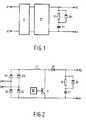
- K1 and K2form input terminals for connection to a supply voltage source.
- Iare rectifying means coupled to the input terminals for rectifying an AC voltage supplied by the supply voltage source.
- Output terminals of rectifying means Iare connected to respective input terminals of a DC-DC converter II.
- the construction of the DC-DC converteris not shown in Fig. 1.
- the DC-DC convertercomprises a switching element, first inductive means, and a first unidirectional element.
- Output terminals K3 and K4 of the DC-DC converter IIform output terminals of the means for generating a DC voltage for the connection of a load and are interconnected by a series arrangement of resistor R1 and capacitor C1 which in this embodiment form an impedance and first capacitive means, respectively.
- Resistor R1is shunted by diode D5 which in this embodiment forms a further unidirectional element.
- Resistor R1 and capacitor C1 in this embodimentform a circuit branch.
- the operation of the circuit shown in Fig. 1is as follows.
- the terminals K1 and K2are connected to a supply voltage source which delivers an AC voltage
- this AC voltageis rectified by the rectifying means I during stationary operation of the circuit arrangement.
- the rectified AC voltageis converted by the DC-DC converter into an output DC voltage consisting of a substantially constant DC voltage with a periodic voltage superimposed thereon with a frequency which is equal to twice the frequency of the AC voltage.
- This periodic voltageis caused by the alternation of charging of the capacitor C1 through resistor R1 and discharging of the capacitor C1 through diode D5.
- the loadis supplied with the discharging current of capacitor C1.
- Diodes D1, D2, D3 and D4form a diode bridge which in this embodiment forms rectifying means coupled to the input terminals.
- Control signal generator m, switching element S1, diode D6 and coil L1together form a DC-DC converter of the up-converter type, connected between the rectifying means and the output terminals.
- Diode D6 and coil L1form a first unidirectional element and first inductive means, respectively.
- the control signal generatorDuring stationary operation of the embodiment shown in Fig. 2, the control signal generator generates a high-frequency control signal for rendering the switching element S1 conducting and non-conducting. This transmutes the rectified AC voltage into the output DC voltage.
- the duty cycle of the control signalis proportional to the instantaneous value of the rectified AC voltage in order to improve the power factor of the circuit arrangement. This achieves at the same time that the power dissipated in the impedance is comparatively small during stationary lamp operation.
- the average value of the output AC voltageis also controlled through the duty cycle of the control signal.
- the circuit components which are necessary for realising these two control functionsare not shown in Fig. 2.
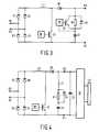
- the circuit arrangement shown in Fig. 3comprises, besides the circuit components corresponding to those also forming part of the circuit arrangement shown in Fig. 2, a switching element S2 which shunts the resistor R1.
- the circuit arrangementalso comprises a control circuit IV coupled to a control electrode of switching element S2.
- An input of control circuit IVis coupled to a common junction point of capacitor C1 and resistor R1. This coupling is indicated with a broken line in Fig. 3.
- the switching element S2is non-conducting and accordingly does not conduct the comparatively strong current with which capacitor C1 is charged.
- control circuit IVrenders the switching element S2 conducting so that the capacitor C1 is charged mainly through the switching element S2 during stationary operation, whereby power dissipation in resistor R1 during stationary operation is prevented.
- the operation of the circuit arrangement shown in Fig. 3corresponds to that of the circuit arrangement shown in Fig. 2 in all other respects.
- the circuit arrangement shown in Fig. 4differs from that shown in Fig. 2 in that a coil L2 is included in series with resistor R1 and forms further inductive means in this embodiment.
- Output terminals K3 and K4are in addition interconnected through a capacitor C2.
- the capacitor C2 in this embodimentforms further capacitive means.
- the output terminals K3 and K4are connected to respective inputs of DC-AC converter V.
- a lamp Lais connected to output terminals of the DC-AC converter V.
- the current with which capacitor C1 is chargedis limited by resistor R1 immediately after the connection of the input terminals K1 and K2 to the supply voltage source.
- the DC-AC convertergenerates a high-frequency current with which the lamp is supplied during stationary operation.
- the generation of the high-frequency current by the DC-AC convertercauses a high-frequency voltage component to be present across capacitor C1 and resistor R1 during stationary lamp operation.
- This high-frequency voltage componentgives rise to a further power dissipation in capacitor C1 and resistor R1.
- Coil L2 and capacitor C2act as a high-frequency filter, so that the amplitude of the high-frequency voltage component is comparatively low, as is the power dissipation caused by this voltage component.
- the capacitance of capacitor C1was 22 ⁇ F.
- the resistance of R1was approximately 20 Ohms
- the self-inductance of coil L2was 400 ⁇ H
- the capacitance of capacitor C2was 180 nF.
- the circuit arrangementwas supplied with a sinusoidal AC voltage with an effective value of 230 V.
- the duty cycle of the switching element of the up-converterwas proportional to the instantaneous amplitude of the full-wave rectified AC voltage. It was found that the inrush current was satisfactorily limited by the resistor R1.
- the power dissipated in the resistor during stationary lamp operationwas no more than approximately 0.34 W.
- the power dissipated in the resistor during stationary lamp operationwas approximately 1.95 W when the resistor R1, the capacitor C1, and the diode D5 were directly connected to the output of the diode bridge and the filter comprising coil L2 and capacitor C2 was omitted.
Landscapes
- Engineering & Computer Science (AREA)
- Power Engineering (AREA)
- Circuit Arrangements For Discharge Lamps (AREA)
- Dc-Dc Converters (AREA)
Abstract
Description
- input terminals for connection to a supply voltage source,
- rectifying means coupled to the input terminals for rectifying an AC voltagesupplied by the supply voltage source,
- output terminals for connection to the load,
- a DC-DC converter connected between the rectifying means and the outputterminals and provided with first inductive means, a first unidirectional element,and a switching element, and
- first capacitive means coupled to the output terminals.
Claims (8)
- A circuit arrangement for supplying a load which comprises a lamp,comprising means for generating a DC voltage provided withcharacterized in that the output terminals are interconnected by a circuit branch whichcomprises a series arrangement of an impedance (R1) and the first capacitive means, whichimpedance is shunted by a further unidirectional element (D5).input terminals (K1,K2) for connection to a supply voltage source,rectifying means (D1..D4) coupled to the input terminals for rectifying an AC voltagesupplied by the supply voltage source,output terminals for connection to the load,a DC-DC converter connected between the rectifying means and the outputterminals and provided with first inductive means, a first unidirectional element,and a switching element (S1), andfirst capacitive means (C1) coupled to the output terminals,
- A circuit arrangement as claimed in Claim 1, wherein the impedancecomprises an ohmic resistor.
- A circuit arrangement as claimed in Claim 1, wherein the impedancecomprises an inductive element.
- A circuit arrangement as claimed in any one of the preceding Claims,wherein the DC-DC converter comprises an up-converter.
- A circuit arrangement as claimed in any one or several of the precedingClaims, wherein the circuit arrangement in addition comprises a DC-AC converter coupled tothe output terminals for generating a current of alternating polarity.
- A circuit arrangement as claimed in Claim 5, wherein the circuit branchin addition comprises further inductive means, and the circuit arrangement comprises furthercapacitive means which shunt the circuit branch.
- A circuit arrangement as claimed in Claim 6, wherein the impedance andfurther inductive means have been integrated into one component.
- A circuit arrangement as claimed in any one or several of the precedingClaims, wherein the impedance is shunted by a switching element.
Priority Applications (1)
| Application Number | Priority Date | Filing Date | Title |
|---|---|---|---|
| EP95919603AEP0715779B1 (en) | 1994-06-28 | 1995-06-12 | Circuit arrangement |
Applications Claiming Priority (4)
| Application Number | Priority Date | Filing Date | Title |
|---|---|---|---|
| EP94201859 | 1994-06-28 | ||
| EP94201859 | 1994-06-28 | ||
| EP95919603AEP0715779B1 (en) | 1994-06-28 | 1995-06-12 | Circuit arrangement |
| PCT/IB1995/000467WO1996001002A1 (en) | 1994-06-28 | 1995-06-12 | Circuit arrangement |
Publications (2)
| Publication Number | Publication Date |
|---|---|
| EP0715779A1 EP0715779A1 (en) | 1996-06-12 |
| EP0715779B1true EP0715779B1 (en) | 1998-09-30 |
Family
ID=8216993
Family Applications (1)
| Application Number | Title | Priority Date | Filing Date |
|---|---|---|---|
| EP95919603ARevokedEP0715779B1 (en) | 1994-06-28 | 1995-06-12 | Circuit arrangement |
Country Status (8)
| Country | Link |
|---|---|
| US (1) | US6320357B1 (en) |
| EP (1) | EP0715779B1 (en) |
| JP (1) | JP3422999B2 (en) |
| KR (1) | KR100345589B1 (en) |
| CN (1) | CN1048830C (en) |
| DE (1) | DE69505091T2 (en) |
| ES (1) | ES2123986T3 (en) |
| WO (1) | WO1996001002A1 (en) |
Families Citing this family (30)
| Publication number | Priority date | Publication date | Assignee | Title |
|---|---|---|---|---|
| IL120348A (en) | 1997-02-27 | 2002-11-10 | Laser Ind Ltd | Light protection system |
| US8346337B2 (en) | 1998-04-30 | 2013-01-01 | Abbott Diabetes Care Inc. | Analyte monitoring device and methods of use |
| US8480580B2 (en) | 1998-04-30 | 2013-07-09 | Abbott Diabetes Care Inc. | Analyte monitoring device and methods of use |
| US8465425B2 (en) | 1998-04-30 | 2013-06-18 | Abbott Diabetes Care Inc. | Analyte monitoring device and methods of use |
| US8974386B2 (en) | 1998-04-30 | 2015-03-10 | Abbott Diabetes Care Inc. | Analyte monitoring device and methods of use |
| US8688188B2 (en) | 1998-04-30 | 2014-04-01 | Abbott Diabetes Care Inc. | Analyte monitoring device and methods of use |
| US6175752B1 (en) | 1998-04-30 | 2001-01-16 | Therasense, Inc. | Analyte monitoring device and methods of use |
| US9066695B2 (en) | 1998-04-30 | 2015-06-30 | Abbott Diabetes Care Inc. | Analyte monitoring device and methods of use |
| US6949816B2 (en) | 2003-04-21 | 2005-09-27 | Motorola, Inc. | Semiconductor component having first surface area for electrically coupling to a semiconductor chip and second surface area for electrically coupling to a substrate, and method of manufacturing same |
| DE19830368A1 (en)* | 1998-07-07 | 2000-02-03 | Patent Treuhand Ges Fuer Elektrische Gluehlampen Mbh | Electronic ballast with inrush current limitation |
| DE19832580A1 (en)* | 1998-07-08 | 2000-01-13 | Carros Werner Reinhold | D.c. controller for converting 120 Volts a.c., 60 Hz to 200 Volts d.c. for continuous universal and d.c. motor speed regulation achieves high output power with small size and wt. |
| DE29813902U1 (en) | 1998-07-23 | 1999-06-17 | Carros Werner Reinhold Dipl In | DC chopper |
| US6560471B1 (en) | 2001-01-02 | 2003-05-06 | Therasense, Inc. | Analyte monitoring device and methods of use |
| JP4159365B2 (en)* | 2001-03-16 | 2008-10-01 | コーニンクレッカ フィリップス エレクトロニクス エヌ ヴィ | DC-DC converter |
| EP1397068A2 (en) | 2001-04-02 | 2004-03-17 | Therasense, Inc. | Blood glucose tracking apparatus and methods |
| US6714429B2 (en)* | 2001-08-15 | 2004-03-30 | Astec International Limited | Active inrush current control for AC to DC converters |
| US6798177B1 (en)* | 2002-10-15 | 2004-09-28 | Arques Technology, Inc. | Boost-buck cascade converter for pulsating loads |
| JP4227491B2 (en)* | 2003-09-09 | 2009-02-18 | 株式会社リコー | Power supply circuit for digital camera |
| DE102004015004A1 (en)* | 2004-03-26 | 2005-10-13 | Enocean Gmbh | Arrangement with at least one electrical voltage source and a first voltage converter circuit |
| US20060132105A1 (en)* | 2004-12-16 | 2006-06-22 | Prasad Atluri R | Controlling inrush current |
| US20060274468A1 (en)* | 2005-06-03 | 2006-12-07 | Phadke Vijay G | Active inrush current control using a relay for AC to DC converters |
| WO2007143225A2 (en) | 2006-06-07 | 2007-12-13 | Abbott Diabetes Care, Inc. | Analyte monitoring system and method |
| CN100468932C (en)* | 2006-06-27 | 2009-03-11 | 致新科技股份有限公司 | Initial voltage establishing circuit for switching type voltage converter |
| US8299773B2 (en)* | 2009-07-10 | 2012-10-30 | Delta Electronics, Inc. | System and method for limiting input-current surge in a switching mode power supply |
| CN102652464B (en)* | 2009-12-11 | 2015-09-16 | 皇家飞利浦电子股份有限公司 | A driver circuit for driving a load circuit |
| DE102011089553A1 (en)* | 2011-12-22 | 2013-06-27 | Robert Bosch Gmbh | Electronic ballast for a gas discharge lamp |
| JP6463595B2 (en)* | 2013-04-18 | 2019-02-06 | 富士通コンポーネント株式会社 | Pulse motor drive circuit |
| JP6205281B2 (en)* | 2014-01-30 | 2017-09-27 | 新電元工業株式会社 | Power supply |
| FR3067872B1 (en)* | 2017-06-15 | 2020-03-06 | Valeo Vision | STABILIZED ELECTRICAL SUPPLY IN PULSE WIDTH MODULATION |
| DK3794908T3 (en)* | 2018-05-18 | 2022-03-14 | Signify Holding Bv | DISCHARGE CIRCUIT DESIGN TO REMOVE PIT CURRENT IN REPLACEMENT MODULES |
Citations (1)
| Publication number | Priority date | Publication date | Assignee | Title |
|---|---|---|---|---|
| EP0323676A1 (en)* | 1988-01-06 | 1989-07-12 | Koninklijke Philips Electronics N.V. | Electric arrangement for igniting and supplying a gas discharge lamp |
Family Cites Families (6)
| Publication number | Priority date | Publication date | Assignee | Title |
|---|---|---|---|---|
| US5019952A (en)* | 1989-11-20 | 1991-05-28 | General Electric Company | AC to DC power conversion circuit with low harmonic distortion |
| NZ243218A (en)* | 1991-06-19 | 1996-02-27 | Golden Power Electronics Pty L | Power supply for fluorescent lamp has capacitor bank connected between rectifier input and output to reduce harmonic distortion of ac supply current |
| DE4126865A1 (en)* | 1991-08-14 | 1993-02-18 | Hella Kg Hueck & Co | CIRCUIT ARRANGEMENT FOR STARTING AND OPERATING HIGH PRESSURE GAS DISCHARGE LAMPS |
| US5179508A (en) | 1991-10-15 | 1993-01-12 | International Business Machines Corp. | Standby boost converter |
| US5402331A (en)* | 1992-02-25 | 1995-03-28 | Matsushita Electric Works | Power device |
| JP3136451B2 (en)* | 1992-06-23 | 2001-02-19 | 株式会社小糸製作所 | Lighting circuit for vehicle discharge lamps |
- 1995
- 1995-06-12EPEP95919603Apatent/EP0715779B1/ennot_activeRevoked
- 1995-06-12DEDE69505091Tpatent/DE69505091T2/ennot_activeExpired - Fee Related
- 1995-06-12ESES95919603Tpatent/ES2123986T3/ennot_activeExpired - Lifetime
- 1995-06-12KRKR1019960700934Apatent/KR100345589B1/ennot_activeExpired - Fee Related
- 1995-06-12WOPCT/IB1995/000467patent/WO1996001002A1/ennot_activeApplication Discontinuation
- 1995-06-12CNCN95190691Apatent/CN1048830C/ennot_activeExpired - Fee Related
- 1995-06-12JPJP50297096Apatent/JP3422999B2/ennot_activeExpired - Fee Related
- 1997
- 1997-05-23USUS08/862,836patent/US6320357B1/ennot_activeExpired - Fee Related
Patent Citations (1)
| Publication number | Priority date | Publication date | Assignee | Title |
|---|---|---|---|---|
| EP0323676A1 (en)* | 1988-01-06 | 1989-07-12 | Koninklijke Philips Electronics N.V. | Electric arrangement for igniting and supplying a gas discharge lamp |
Also Published As
| Publication number | Publication date |
|---|---|
| CN1131476A (en) | 1996-09-18 |
| EP0715779A1 (en) | 1996-06-12 |
| DE69505091T2 (en) | 1999-05-20 |
| KR960704385A (en) | 1996-08-31 |
| DE69505091D1 (en) | 1998-11-05 |
| WO1996001002A1 (en) | 1996-01-11 |
| JPH09502599A (en) | 1997-03-11 |
| JP3422999B2 (en) | 2003-07-07 |
| CN1048830C (en) | 2000-01-26 |
| ES2123986T3 (en) | 1999-01-16 |
| KR100345589B1 (en) | 2002-11-11 |
| US6320357B1 (en) | 2001-11-20 |
Similar Documents
| Publication | Publication Date | Title |
|---|---|---|
| EP0715779B1 (en) | Circuit arrangement | |
| US4959591A (en) | Rectifier-inverter circuit with low harmonic feedback, particularly for operation of fluorescent lamps | |
| US5172033A (en) | Discharge lamp operating inverter circuit with electric dimmer utilizing frequency control of the inverter | |
| US6069453A (en) | Ballast circuit for reducing striations in a discharge lamp | |
| US6043606A (en) | Discharge lamp device having a preheating electrode circuit | |
| EP0838128B1 (en) | Circuit arrangement | |
| US5400241A (en) | High frequency discharge lamp | |
| US5986408A (en) | Discharge lamp with heating electrode circuit | |
| WO2002075908A1 (en) | Dc-dc converter. | |
| US5652480A (en) | Electronic ballast incorporating a clocked switching controller | |
| EP0599405B1 (en) | Low harmonic power supply for a discharge lamp | |
| EP0479196A1 (en) | Power supply circuit | |
| JPH09238466A (en) | Power supply device, discharge lamp lighting device and lighting device | |
| EP0860097B1 (en) | Circuit arrangement | |
| US6294882B1 (en) | Circuit arrangement with improved power-factor for feeding a discharge lamp | |
| US6310790B1 (en) | High frequency DC-DC down converter with power feedback for improved power factor | |
| US5589739A (en) | Hybrid ballast for high pressure discharge lamp | |
| JP3733675B2 (en) | Inverter device, discharge lamp lighting device and lighting device | |
| US5917717A (en) | Ballast dimmer with passive power feedback control | |
| US6492780B1 (en) | Lamp ballast system | |
| JPH07194142A (en) | Discharge lamp lighting device | |
| JPH06284739A (en) | Electric-discharge lamp lighting device | |
| JPS63245280A (en) | power supply | |
| JPH05219723A (en) | Power supply and discharge lamp lighting device | |
| JPH09504650A (en) | Circuit device |
Legal Events
| Date | Code | Title | Description |
|---|---|---|---|
| PUAI | Public reference made under article 153(3) epc to a published international application that has entered the european phase | Free format text:ORIGINAL CODE: 0009012 | |
| AK | Designated contracting states | Kind code of ref document:A1 Designated state(s):BE DE ES FR GB IT NL | |
| 17P | Request for examination filed | Effective date:19960711 | |
| GRAG | Despatch of communication of intention to grant | Free format text:ORIGINAL CODE: EPIDOS AGRA | |
| 17Q | First examination report despatched | Effective date:19971126 | |
| GRAG | Despatch of communication of intention to grant | Free format text:ORIGINAL CODE: EPIDOS AGRA | |
| GRAH | Despatch of communication of intention to grant a patent | Free format text:ORIGINAL CODE: EPIDOS IGRA | |
| GRAH | Despatch of communication of intention to grant a patent | Free format text:ORIGINAL CODE: EPIDOS IGRA | |
| GRAA | (expected) grant | Free format text:ORIGINAL CODE: 0009210 | |
| AK | Designated contracting states | Kind code of ref document:B1 Designated state(s):BE DE ES FR GB IT NL | |
| PG25 | Lapsed in a contracting state [announced via postgrant information from national office to epo] | Ref country code:NL Free format text:LAPSE BECAUSE OF FAILURE TO SUBMIT A TRANSLATION OF THE DESCRIPTION OR TO PAY THE FEE WITHIN THE PRESCRIBED TIME-LIMIT Effective date:19980930 Ref country code:BE Free format text:LAPSE BECAUSE OF FAILURE TO SUBMIT A TRANSLATION OF THE DESCRIPTION OR TO PAY THE FEE WITHIN THE PRESCRIBED TIME-LIMIT Effective date:19980930 | |
| REF | Corresponds to: | Ref document number:69505091 Country of ref document:DE Date of ref document:19981105 | |
| ET | Fr: translation filed | ||
| REG | Reference to a national code | Ref country code:ES Ref legal event code:FG2A Ref document number:2123986 Country of ref document:ES Kind code of ref document:T3 | |
| NLV1 | Nl: lapsed or annulled due to failure to fulfill the requirements of art. 29p and 29m of the patents act | ||
| PLBQ | Unpublished change to opponent data | Free format text:ORIGINAL CODE: EPIDOS OPPO | |
| PLBI | Opposition filed | Free format text:ORIGINAL CODE: 0009260 | |
| PLBF | Reply of patent proprietor to notice(s) of opposition | Free format text:ORIGINAL CODE: EPIDOS OBSO | |
| 26 | Opposition filed | Opponent name:OY HELVAR Effective date:19990629 | |
| PLBF | Reply of patent proprietor to notice(s) of opposition | Free format text:ORIGINAL CODE: EPIDOS OBSO | |
| REG | Reference to a national code | Ref country code:GB Ref legal event code:IF02 | |
| PGFP | Annual fee paid to national office [announced via postgrant information from national office to epo] | Ref country code:ES Payment date:20020610 Year of fee payment:8 | |
| PGFP | Annual fee paid to national office [announced via postgrant information from national office to epo] | Ref country code:FR Payment date:20020625 Year of fee payment:8 | |
| PGFP | Annual fee paid to national office [announced via postgrant information from national office to epo] | Ref country code:GB Payment date:20020628 Year of fee payment:8 | |
| PGFP | Annual fee paid to national office [announced via postgrant information from national office to epo] | Ref country code:DE Payment date:20020821 Year of fee payment:8 | |
| RDAH | Patent revoked | Free format text:ORIGINAL CODE: EPIDOS REVO | |
| REG | Reference to a national code | Ref country code:FR Ref legal event code:D6 | |
| REG | Reference to a national code | Ref country code:GB Ref legal event code:746 Effective date:20021111 | |
| RDAG | Patent revoked | Free format text:ORIGINAL CODE: 0009271 | |
| STAA | Information on the status of an ep patent application or granted ep patent | Free format text:STATUS: PATENT REVOKED | |
| 27W | Patent revoked | Effective date:20021116 | |
| GBC | Gb: translation of claims filed (gb section 78(7)/1977) | Free format text:20021116 |