EP0715334B1 - Plasma reactors for processing semiconductor wafers - Google Patents
Plasma reactors for processing semiconductor wafersDownload PDFInfo
- Publication number
- EP0715334B1 EP0715334B1EP95307269AEP95307269AEP0715334B1EP 0715334 B1EP0715334 B1EP 0715334B1EP 95307269 AEP95307269 AEP 95307269AEP 95307269 AEP95307269 AEP 95307269AEP 0715334 B1EP0715334 B1EP 0715334B1
- Authority
- EP
- European Patent Office
- Prior art keywords
- power
- chamber
- circuit
- plasma
- coupler
- Prior art date
- Legal status (The legal status is an assumption and is not a legal conclusion. Google has not performed a legal analysis and makes no representation as to the accuracy of the status listed.)
- Expired - Lifetime
Links
Images


Classifications
- H—ELECTRICITY
- H01—ELECTRIC ELEMENTS
- H01L—SEMICONDUCTOR DEVICES NOT COVERED BY CLASS H10
- H01L21/00—Processes or apparatus adapted for the manufacture or treatment of semiconductor or solid state devices or of parts thereof
- H01L21/02—Manufacture or treatment of semiconductor devices or of parts thereof
- H01L21/04—Manufacture or treatment of semiconductor devices or of parts thereof the devices having potential barriers, e.g. a PN junction, depletion layer or carrier concentration layer
- H01L21/18—Manufacture or treatment of semiconductor devices or of parts thereof the devices having potential barriers, e.g. a PN junction, depletion layer or carrier concentration layer the devices having semiconductor bodies comprising elements of Group IV of the Periodic Table or AIIIBV compounds with or without impurities, e.g. doping materials
- H—ELECTRICITY
- H01—ELECTRIC ELEMENTS
- H01J—ELECTRIC DISCHARGE TUBES OR DISCHARGE LAMPS
- H01J37/00—Discharge tubes with provision for introducing objects or material to be exposed to the discharge, e.g. for the purpose of examination or processing thereof
- H01J37/32—Gas-filled discharge tubes
- H01J37/32009—Arrangements for generation of plasma specially adapted for examination or treatment of objects, e.g. plasma sources
- H01J37/32082—Radio frequency generated discharge
- H01J37/32174—Circuits specially adapted for controlling the RF discharge
- H—ELECTRICITY
- H01—ELECTRIC ELEMENTS
- H01J—ELECTRIC DISCHARGE TUBES OR DISCHARGE LAMPS
- H01J37/00—Discharge tubes with provision for introducing objects or material to be exposed to the discharge, e.g. for the purpose of examination or processing thereof
- H01J37/32—Gas-filled discharge tubes
- H01J37/32009—Arrangements for generation of plasma specially adapted for examination or treatment of objects, e.g. plasma sources
- H01J37/32082—Radio frequency generated discharge
- H—ELECTRICITY
- H01—ELECTRIC ELEMENTS
- H01J—ELECTRIC DISCHARGE TUBES OR DISCHARGE LAMPS
- H01J37/00—Discharge tubes with provision for introducing objects or material to be exposed to the discharge, e.g. for the purpose of examination or processing thereof
- H01J37/32—Gas-filled discharge tubes
- H01J37/32917—Plasma diagnostics
- H01J37/32935—Monitoring and controlling tubes by information coming from the object and/or discharge
- H—ELECTRICITY
- H01—ELECTRIC ELEMENTS
- H01J—ELECTRIC DISCHARGE TUBES OR DISCHARGE LAMPS
- H01J37/00—Discharge tubes with provision for introducing objects or material to be exposed to the discharge, e.g. for the purpose of examination or processing thereof
- H01J37/32—Gas-filled discharge tubes
- H01J37/32917—Plasma diagnostics
- H01J37/3299—Feedback systems
- H—ELECTRICITY
- H05—ELECTRIC TECHNIQUES NOT OTHERWISE PROVIDED FOR
- H05H—PLASMA TECHNIQUE; PRODUCTION OF ACCELERATED ELECTRICALLY-CHARGED PARTICLES OR OF NEUTRONS; PRODUCTION OR ACCELERATION OF NEUTRAL MOLECULAR OR ATOMIC BEAMS
- H05H1/00—Generating plasma; Handling plasma
- H05H1/24—Generating plasma
- H05H1/46—Generating plasma using applied electromagnetic fields, e.g. high frequency or microwave energy
Definitions
- the inventionis related to high frequency capacitively coupled radio frequency (RF) plasma reactors for semiconductor wafers and in particular to improvements in the control of the RF source power level and to protection of the wafer pedestal from damage during chamber cleaning operations.
- RFradio frequency
- a plasma chamber 10 operating at a high RF frequency(e.g. 13.56 MHz) holds a semiconductor wafer or substrate (not shown) and performs a desired process on the wafer, such as plasma etching, plasma-enhanced chemical vapour deposition, or sputtering .
- RF poweris furnished to the chamber 10 by a conventional 13.56 MHz RF generator 12 via a transmission line 14 (such as a 50 ohm coaxial cable) and a variable RF match circuit 16.
- the convention al RF generator 12includes a 13.56 MHz RF power source 12a, an output stage 12b, and a conventional dual directional coupler 12c.
- the output stge 12bmatches the non-standard output impedance of the RF power circuit 12a to the industry standard characteristic impedance of the coaxial cable of 50 ohms.
- the dual directional coupler 12cprovides outputs 18a, 18b indicative of the forward and reflected RF power at the output of the output stage 12b.
- a conventional feedback control circuit 20governs the variable RF match circuit in such a manner as to minimize the VSWR, that is, to minimize the reflected RF power sensed at the reflected power output 18b of the dual directional coupler.
- the control circuitadjusts the variable RF match network so as to transform the impedance of the plasma chamber to the 50 ohm characteristic impedance of the coaxial cable. Since the plasma chamber impedance tends to vary during wafer processing, the variable RF match circuit 16 maintains an RF match by changing its impedance to compensate for fluctuations in the plasma chamber impedance.
- EP-A-0058820discloses such an RF generator system for supporting ionizing power to gases in a dry process wafer etching system.
- the generatorprovides power to the load via a transmission line and load impedance is automatically matched to the surge impedance of the transmission to provide maximum transfer of energy from the generator to the load.
- Voltages representative of input power and reflected powerare utilized to control a match circuit to cause load impedance to equal transmission time impedance.
- Feedback loop meansare also provided to maintain net load power at an extendably commanded level.
- JP-A-58 073848also discloses an arrangement for ensuring a constant power consumption irrespective of variation in local impedance by maintaining a constant difference between an incident wave power to the load and the reflected power from the load.
- variable RF match circuit and its feedback control circuit to maintain a low VSWRare essential for three reasons: (1) It provides a constant load impedance to the output stage of the RF generator, so that the generator will supply a constant RF power level to the plasma chamber. Fluctuations in the RF power level would cause instability and unpredictability in the semiconductor processing performed by the plasma chamber. (2) It avoids the high peak voltages associated with a high VSWR on the transmission line 14, which high voltages could damage the transmission line. (3) It avoids the high peak currents associated with a high VSWR on the transmission line, which currents could cause overheating of the transmission line which could change its characteristic impedance, thereby causing nonuniform chamber process conditions depending on the temperature history of the transmission line.
- variable RF match circuit 16is expensive and bulky. Furthermore, variable RF match networks which employ moving parts tend to be unreliable. However, at the high RF power levels of 1200 Watts required for chemical vapor deposition processes or 2000 Watts required for etch or chamber cleaning operations, the variable RF match network 14 has seemed indispensable at high RF frequencies on the order of 13.56 MHz.
- a low frequency (e.g., 350 kHz) RF generator 12'has a low frequency power circuit 12a' in lieu of the high frequency power circuit 12a of Figure 1A.
- the low frequency RF generator 12'is coupled through a fixed RF match network 30 to the plasma chamber 10. Because the RF frequency is so low, the transmission line between the RF generator and the plasma chamber generally is much shorter than a quarter wavelength, so that no standing wave pattern occurs in the transmission line. Therefore the above-mentioned problems (2) and (3) of excessive peak voltages and peak currents will not occur even if there is a mismatch between the plasma chamber impedance and the transmission line.
- a control circuit 32dynamically adjusts the power level of the RF power circuit 12a to maintain the delivered RF power (i.e. the difference between the forward power 18a and reflected power 18b) at a constant level. Since this control circuit makes the RF power level independent of moderate changes in load impedance, this design omits the variable RF match circuit and its feedback control 20, and substitutes a fixed RF match network 30.
- the fixed RF match network 30has a fixed output impedance which is selected to match the average impedance of the plasma inside the chamber 10 over time.
- the transmission line 14is short compared to a quarter wavelength, it does not matter which end of the transmission line the match network is connected to, so for convenience the fixed RF match circuit 30 can be included as a component within the RF power generator 12'.
- the control circuit 32includes a first subtractor node 34 which senses delivered RF power (i.e., the difference between the forward power and reflected power outputs 18a, 18b of the dual directional coupler 12c) and a second subtractor node 36 which senses the difference between the delivered RF power and a desired RF power set by the user.
- the desired power levelis depicted as a variable analog power source 38 applied to one input of the subtractor node 36, although the source 38 may be digital and the comparison may be carried out digitally by the subtraction node 36.
- the output of the second subtracter nodeis applied as an error signal to a control input of the RF power circuit 12a.
- the RF power circuit 12aresponds to the error signal by either increasing or decreasing the output power level, depending upon the sign of the error signal. This servos the power output level of the RF power circuit 12a to minimize or null the error signal so that the delivered power is maintained at the desired power level.
- the error signal applied to the control input of the RF power circuit 12ais zero in the absence of fluctuations in the plasma impedance.
- the low frequency RF plasma system of Figure 1Badvantageously avoids the need for an expensive, potentially unreliable, variable RF match circuit.
- a variable RF match circuitat higher RF frequencies, such as the commonly used frequency of 13.56 MHz.
- This inventionprovides a high frequency RF plasma system for processing a semiconductor substrate, comprising a plasma chamber adapted to receive a semiconductor substrate and a process gas therein, a coupling device for coupling RF energy to the process gas inside the chamber, and an RF power generator mounted adjacent to the plasma chamber, including an RF power source for producing RF energy, an RF impedance matching circuit connected between the RF power source and the coupling device, a power sensing coupler connected in series with the match circuit between the RF power source and the coupling device, said power sensing coupler having a measurement output indicating the amount of RF power delivered through the coupler, and a control circuit coupled to said measurement output of said power sensing coupler and connected to said RF power circuit (12a) to govern the amount of RF power produced by said RF power circuit so as to maintain the delivered power measured by the coupler at a predetermined level, wherein said RF power source produces RF energy having a frequency of at least 1 MHz, the power source having an output located at a distance from the coup
- the inventionprovides a plasma reactor system according to claim 9.
- the RF power source and fixed match circuitare mounted directly on the plasma chamber to minimize such distance.
- the inventionalso includes apparatus for detecting the endpoint of an etch or cleaning process by detecting when the reflected power or VSWR ceases to change as a function of the removal of the substance being etched or cleaned.
- Figure 1Ais a simplified block diagram of a high frequency plasma reactor and RF control system of the prior art.
- Figure 1Bis a simplified block diagram of a low frequency plasma reactor and RF control system of the prior art.
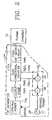
- Figure 2is a block diagram of a plasma reactor and RF control system of a first embodiment of the invention.
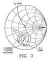
- Figure 3is a Smith chart corresponding to the embodiment of Figure 2.
- Figure 4is a block diagram of a plasma reactor and RF control system of a second embodiment of the invention.
- the present inventionmay be used with any plasma chamber for processing semiconductor wafers or substrates, such as plasma etch chambers and plasma-enhanced deposition chambers.
- the chambermay using any conventional device for electrically coupling RF power into the chamber, such as electrodes for capacitive coupling, a coil for inductive coupling, or an antenna for electromagnetic coupling of RF power into the chamber.
- the inventionemploys a novel high frequency RF generator 12" having the same topology as the prior art low frequency RF generator 12' of Figure 1B.
- a high frequencyis considered a frequency of at least 1 MHz.
- our designuses a fixed RF match and includes a control circuit 32 which maintains delivered RF power at a desired level.
- Our designhas a high frequency power source 12a in lieu of the low frequency power source 12' of Figure 1B.
- our designavoids the need for a variable RF match circuit by locating the RF generator a very short distance from the electrode, inductor, antenna, or other RF coupling device in the plasma chamber 10 to which the RF power is being delivered, specifically, a distance which is much less than an eighth of a wavelength at the frequency of the RF generator.
- the RF signalhas a wavelength in a typical coaxial transmission line of about 15 meters, so that an eighth of a wavelength would be aboue 2 meters.
- the RF generator 12"is mounted directly on the plasma chamber 10 so that there is negligible distance separating the two components. The elimination of a long transmission line between the RF generator and the plasma chamber allows us to substitute a relatively inexpensive, compact, and reliable fixed RF match circuit 30 in place of the much more expensive and often less reliable RF match circuit 16 used in conventional high frequency RF power systems.
- the use of a fixed RF matchmeans the RF generator will experience all fluctuations in the load impedance of the plasma chamber.
- the controller 32maintains a constant delivered power (forward power minus reflected power) in spite of changes in the plasma chamber load impedance during processes performed within the chamber.
- the principles for designing an RF match circuit to match the output impedance of an RF generator to the impedance of a loadare well known.
- the RF matchcontains inductors (L) and/or capacitors (C) whose values are chosen according to straightforward design equations to match given input and output impedances at a given frequency.
- Linductors
- Ccapacitors
- the design equationsare described in the following reference books, the complete contents of which are hereby incorporated by reference into this patent application: "Reflections-Transmission Lines and Antennas" by Walter Maxwell (1990); and “Radio Frequency Transistors - Principles and Practical Applications” by Norm Dye and Helge Granberg (1993).
- the RF match circuitshould be optimised to maintain the VSWR, caused by the impedance mismatch between the output impedance of the RF generator and the impedance of the plasma reactor load, below a value at which the RF generator can safely supply the required delivered power.
- Most RF generatorscan tolerate a higher VSWR when operating below their rated maximum output power. Therefore, the RF match L and C component values should be chosen to provide a relatively low VSWR during the plasma processes that require the highest RF power.
- the Smith chart of Figure 3illustrates the method used to optimise the RF match circuit 30 in our invention.
- the small squares on the chartrepresent the load impedance of the plasma chamber during different phases of a typical plasma-enhanced chemical vapour deposition (PECVD) process performed within the chamber.
- the small crosses on the chartrepresent the chamber load impedance during different phases of a typical plasma etch process used to clean the chamber between PECVD processes.
- the exemplary CVD processrequires 1200 watts of RF power, and the etch process requires 2000 watts of RF power, both at a frequency of 13.56 MHz.
- the commercially available RF generator used in our examplecan deliver 2000 watts to a load if the VSWR is 2 or less, and can deliver 1200 watts if the VSWR is 3 or less. If the L and C components of the RF match are chosen to match the 40 ohm RF generator output impedance to the chamber "center" impedance indicated by the large dot in Figure 3, then all the crosses fall within the VSWR - 2 circle, and all the squares fall within the VSWR - 3 circle. Therefore, designing the RF match to this "center" impedance accomplishes our objectives.
- the power level regulator circuit in the design shown in Figure 2is identical to the regulator circuit of the prior art system shown in Figure 1B.
- a conventional 50 ohm dual directional coupler 12cprovides the requisite measurements of forward and reflected power 18a, 18b to a control circuit 32.
- the first comparator or subtracter circuit 34determines the power delivered to the load (the plasma chamber) by subtracting the rectified and low pass filtered forward power signal 18a from the reflected power signal 18b.
- a second comparator or subtracter circuit 36compares the delivered power level as so determined with a value 38 representing the desired delivered power. The second comparator adjusts a control sent to the power source 12a according to whether the delivered power is too high or too low.
- the circuitry describedmay be implemented by conventional, straightforward techniques in analog or digital form, or by programming a general purpose microcomputer.
- a variation on the design shown in Figure 2would be to simplify the RF generator by eliminating the output stage 12b which converts the output impedance of the RF power source 12a to the 50 ohm industry standard impedance.
- the L and C components of the fixed RF match circuitthen would be chosen according to well known design equations to match the non-standard output impedance of the RF power source instead of matching 50 ohms.
- the complication presented by this variationis that the dual directional coupler also would have to be designed for this non-standard impedance. Dual directional coupler design principles are also extremely well known, so designing one for a non-standard impedance presents no conceptual difficulty, but it precludes using an "off the shelf" 50 ohm dual directional coupler.
- Figure 4illustrates a further variation of the invention in which the output stage 12b is eliminated as just described, and furthermore the respective positions within the topology of the RF generator circuit 12 of the dual directional coupler and the RF match are swapped.
- An advantage of the embodiment of Figure 4is that the measurements of forward and reflected power provided by the dual directional coupler 54 more accurately indicate the actual power delivered to the plasma chamber.
- the dual directional coupleris measuring the total power delivered to the match network 30 and the plasma chamber 10.
- the power actually delivered to the plasma chamberwill be 90-95% of the power indicated by the dual directional coupler as being delivered.
- the amount of powerwill vary within this range as the impedance presented by the plasma chamber varies under different plasma process conditions. Therefore, there may be up to a 5% unpredictability in the RF power delivered to the chamber.
- the coupler 54By locating the dual directional coupler 54 between the match network 52 and the chamber as shown in Figure 4, the coupler 54 will measure the power actually delivered to the plasma chamber. Therefore, the power delivered to the chamber will be more accurately controlled by the control circuit 32, thereby permitting more uniform and predictable processing of the semiconductor substrate in the chamber.
- the dual directional coupler 54must be designed to operate at the load impedance of the plasma reactor rather than the output impedance of the RF power source.
- control circuits of the embodiments of Figures 2 and 4permit the VSWR, and hence the reflected power to fluctuate rather than attempting to null the reflected power in response to fluctuations in the plasma impedance.
- this featureis exploited during etching or chamber cleaning operations to determine when the substance being etched has been completely removed, or when the chamber has been thoroughly cleaned, so that the etching or cleaning process may be terminated.
- any production waferis removed from the chamber, and then a strong etchant gas is introduced into the chamber while a high level of RF power is applied to the chamber to excite the etchant gas into a plasma state.
- a strong etchant gasis introduced into the chamber while a high level of RF power is applied to the chamber to excite the etchant gas into a plasma state.
- various unwanted depositsare removed from the chamber side walls and pedestal.
- the reactoris normally used to perform chemical vapor deposition of silicon nitride on production wafers, then silicon nitride deposits accumulate over many deposition cycles to the extent that they interfere with the chemical vapor deposition process during subsequent production cycles and must be removed before the reactor can be used again.
- the length of time that the chamber cleaning step must be performed to remove all unwanted depositsis difficult to determine, and so it is customary to perform the cleaning step for an excessive amount of time to guarantee removal of all deposits.
- the unwanted depositsare removed, continuing the chamber cleaning process will etch any exposed metal components within the chamber interior, such as the aluminum chamber walls, the aluminum gas inlet, and the aluminum wafer support pedestal. This etching eventually damages the chamber components to the point where they must be replaced. Therefore, the life of the chamber components could be extended if the etching could be stopped as soon as all the unwanted deposits were removed.
- Our solution to this problemis to sense the change in plasma chamber load impedance during the chamber cleaning operation.
- Such a change in plasma impedanceindicates the removal of deposits from the chamber interior surfaces, because the thickness of deposits on the chamber walls affects the impedance between the metal chamber components and the plasma body.
- our endpoint detection designsenses changes in the plasma impedance by sensing changes in the VSWR or the reflected power, as measured by the dual directional coupler 12c ( Figure 2 or 4). Initially during roughly the first ten seconds of a typical chamber cleaning process, there is no perceptible change in the plasma impedance because the incremental amount of deposits being removed represents a relatively small fraction of the total deposits.
- the plasma chamber load impedancebegins changing noticeably as the layer of deposits continues to diminish.
- the plasma impedancestops changing (or, the rate of change of the plasma impedance falls below a predetermined threshold).
- the completion of the chamber cleaning operationis signaled by the reflected RF power reaching a constant level (or by a reduction in the rate of change of the reflected power below the predetermined threshold). At this time, the chamber cleaning process may be halted.
- an alarm signal to halt the chamber cleaning operationis generated by a microprocessor 70 shown in Figure 4.
- the microprocessor 70is programmed to wait (during the first ten seconds of the chamber cleaning operation) until the plasma impedance first begins to change. Thereafter, the processor continuously determines whether the reflected RF power is changing at a rate of change exceeding a predetermined threshold rate (which, for example, may be zero). Once the rate of change is below the predetermined threshold for a minimum amount of time (e.g., one second), the alarm signal indicating completion of the chamber cleaning operation is transmitted.
- the microprocessor 70has an input port coupled through an analog-to-digital converter 72 to the reflected power output signal 18b from the dual directional coupler 54.
- the microprocessor 70samples the reflected power signal periodically and compares it with the value sampled during the previous processing cycle. If the difference falls below a predetermined value for a predetermined number of processing cycles, then the microprocessor 70 outputs a signal indicating to the user that the chamber cleaning operation is complete and should be halted to avoid excess wear on the chamber interior surfaces. Either the user must halt the chamber cleaning operation or else this signal may be employed to automatically halt the chamber cleaning operation as well as signalling the user. While a digital device (the microprocessor 70 and analog-to-digital converter 72) has been disclosed as providing the "completion-of-chamber clean" signal, the microprocessor 70 may be replaced by a dedicated logic circuit or else an analog circuit.
- the same endpoint detection processalso can be used in a plasma etch chamber to detect when a film being etched from a semiconductor substrate has been completely removed.
- the RF excitation circuit having a fixed RF match networkcan be use equally well with any means for coupling RF power to a plasma, such as a pair of electrodes for capacitively coupling power to the plasma, or an inductor or antenna for inductively coupling power to the plasma. Numerous designs for such power coupling devices are known in the art.
Landscapes
- Physics & Mathematics (AREA)
- Engineering & Computer Science (AREA)
- Plasma & Fusion (AREA)
- Chemical & Material Sciences (AREA)
- Analytical Chemistry (AREA)
- Spectroscopy & Molecular Physics (AREA)
- Electromagnetism (AREA)
- Condensed Matter Physics & Semiconductors (AREA)
- General Physics & Mathematics (AREA)
- Manufacturing & Machinery (AREA)
- Computer Hardware Design (AREA)
- Microelectronics & Electronic Packaging (AREA)
- Power Engineering (AREA)
- Drying Of Semiconductors (AREA)
- Plasma Technology (AREA)
Description
- The invention is related to high frequencycapacitively coupled radio frequency (RF) plasmareactors for semiconductor wafers and in particular toimprovements in the control of the RF source powerlevel and to protection of the wafer pedestal fromdamage during chamber cleaning operations.
- Referring to Figure 1A, there is shown a knownapparatus in which a
plasma chamber 10 operating at ahigh RF frequency (e.g. 13.56 MHz) holds asemiconductor wafer or substrate (not shown) andperforms a desired process on the wafer, such asplasma etching, plasma-enhanced chemical vapourdeposition, or sputtering . In order to maintain aplasma within thechamber 10 RF power is furnished tothechamber 10 by a conventional 13.56MHz RFgenerator 12 via a transmission line 14 (such as a 50ohm coaxial cable) and a variableRF match circuit 16.The convention alRF generator 12 includes a 13.56 MHzRF power source 12a, an output stage 12b, and aconventional dualdirectional coupler 12c. The outputstge 12b matches the non-standard output impedance oftheRF power circuit 12a to the industry standardcharacteristic impedance of the coaxial cable of 50ohms. The dualdirectional coupler 12c providesoutputs 18a, 18b indicative of the forward andreflected RF power at the output of the output stage12b. A conventionalfeedback control circuit 20governs the variable RF match circuit in such a manneras to minimize the VSWR, that is, to minimize thereflected RF power sensed at the reflected poweroutput 18b of the dual directional coupler.Specifically, the control circuit adjusts the variableRF match network so as to transform the impedance ofthe plasma chamber to the 50 ohm characteristicimpedance of the coaxial cable. Since the plasma chamber impedance tends to vary during waferprocessing, the variableRF match circuit 16 maintainsan RF match by changing its impedance to compensatefor fluctuations in the plasma chamber impedance. - EP-A-0058820 discloses such an RF generatorsystem for supporting ionizing power to gases in a dryprocess wafer etching system. The generator providespower to the load via a transmission line and loadimpedance is automatically matched to the surgeimpedance of the transmission to provide maximumtransfer of energy from the generator to the load.Voltages representative of input power and reflectedpower are utilized to control a match circuit to causeload impedance to equal transmission time impedance.Feedback loop means are also provided to maintain netload power at an extendably commanded level.JP-A-58 073848 also discloses an arrangement forensuring a constant power consumption irrespective ofvariation in local impedance by maintaining a constantdifference between an incident wave power to the loadand the reflected power from the load.
- The variable RF match circuit and its feedbackcontrol circuit to maintain a low VSWR are essentialfor three reasons: (1) It provides a constant loadimpedance to the output stage of the RF generator, sothat the generator will supply a constant RF powerlevel to the plasma chamber. Fluctuations in the RFpower level would cause instability andunpredictability in the semiconductor processingperformed by the plasma chamber. (2) It avoids thehigh peak voltages associated with a high VSWR on the
transmission line 14, which high voltages could damagethe transmission line. (3) It avoids the high peakcurrents associated with a high VSWR on thetransmission line, which currents could causeoverheating of the transmission line which couldchange its characteristic impedance, thereby causing nonuniform chamber process conditions depending on thetemperature history of the transmission line. - One problem with the system of Figure 1 is thatthe variable
RF match circuit 16 is expensive andbulky. Furthermore, variable RF match networks whichemploy moving parts tend to be unreliable. However,at the high RF power levels of 1200 Watts required forchemical vapor deposition processes or 2000 Wattsrequired for etch or chamber cleaning operations, thevariableRF match network 14 has seemed indispensableat high RF frequencies on the order of 13.56 MHz. - Referring to Figure 1B, a low frequency (e.g.,350 kHz) RF generator 12' has a low
frequency powercircuit 12a' in lieu of the highfrequency powercircuit 12a of Figure 1A. The low frequency RFgenerator 12' is coupled through a fixedRF matchnetwork 30 to theplasma chamber 10. Because the RFfrequency is so low, the transmission line between theRF generator and the plasma chamber generally is muchshorter than a quarter wavelength, so that no standingwave pattern occurs in the transmission line.Therefore the above-mentioned problems (2) and (3) ofexcessive peak voltages and peak currents will notoccur even if there is a mismatch between the plasmachamber impedance and the transmission line. - However, item (1), the effect of plasma chamberload impedance changes on RF power source outputlevel, still must be addressed. In one known lowfrequency (350 kHz) RF generator design shown inFigure 1B, a
control circuit 32 dynamically adjuststhe power level of theRF power circuit 12a tomaintain the delivered RF power (i.e. the differencebetween theforward power 18a and reflected power 18b)at a constant level. Since this control circuit makesthe RF power level independent of moderate changes inload impedance, this design omits the variable RFmatch circuit and itsfeedback control 20, andsubstitutes a fixedRF match network 30. The fixedRF match network 30 has a fixed output impedance which isselected to match the average impedance of the plasmainside thechamber 10 over time. Since the plasmaimpedance will necessarily fluctuate, there will be RFmismatching and loss of RF power due to powerreflection back to theRF generator 12. Thiscontrasts with the approach of Figure 1A in which thepower level of theRF circuit 12a is maintained at aconstant level and fluctuations in the plasmaimpedance are compensated by changing the impedance ofthevariable match circuit 16 to minimize thereflected RF power. - Since the
transmission line 14 is short comparedto a quarter wavelength, it does not matter which endof the transmission line the match network isconnected to, so for convenience the fixedRF matchcircuit 30 can be included as a component within theRF power generator 12'. - The
control circuit 32 includes afirstsubtractor node 34 which senses delivered RF power(i.e., the difference between the forward power andreflected power outputs 18a, 18b of the dualdirectional coupler 12c) and asecond subtractor node 36 which senses the difference between the deliveredRF power and a desired RF power set by the user. (Inthe diagram of Figure 2, the desired power level isdepicted as a variableanalog power source 38 appliedto one input of thesubtractor node 36, although thesource 38 may be digital and the comparison may becarried out digitally by thesubtraction node 36.)The output of the second subtracter node is applied asan error signal to a control input of theRF powercircuit 12a. TheRF power circuit 12a responds to theerror signal by either increasing or decreasing theoutput power level, depending upon the sign of theerror signal. This servos the power output level oftheRF power circuit 12a to minimize or null the errorsignal so that the delivered power is maintained at the desired power level. The error signal applied tothe control input of theRF power circuit 12a is zeroin the absence of fluctuations in the plasmaimpedance. - The low frequency RF plasma system of Figure 1Badvantageously avoids the need for an expensive,potentially unreliable, variable RF match circuit.However, it has not seemed possible to avoid the useof a variable RF match circuit at higher RFfrequencies, such as the commonly used frequency of13.56 MHz.
- This invention provides a high frequency RFplasma system for processing a semiconductorsubstrate, comprising a plasma chamber adapted toreceive a semiconductor substrate and a process gastherein, a coupling device for coupling RF energy tothe process gas inside the chamber, and an RF powergenerator mounted adjacent to the plasma chamber,including an RF power source for producing RF energy,an RF impedance matching circuit connected between theRF power source and the coupling device, a powersensing coupler connected in series with the matchcircuit between the RF power source and the couplingdevice, said power sensing coupler having ameasurement output indicating the amount of RF powerdelivered through the coupler, and a control circuitcoupled to said measurement output of said powersensing coupler and connected to said RF power circuit(12a) to govern the amount of RF power produced bysaid RF power circuit so as to maintain the deliveredpower measured by the coupler at a predeterminedlevel, wherein said RF power source produces RF energyhaving a frequency of at least 1 MHz, the power sourcehaving an output located at a distance from thecoupling device of substantially less than an eighthof a wavelength at said frequency; and in that the RFimpedance matching circuit has a fixed impedance.
- In a further aspect the invention provides a plasmareactor system according to claim 9.
- Preferably, the RF power source and fixed match circuit are mounted directly on the plasma chamber tominimize such distance.
- Optionally, the invention also includes apparatusfor detecting the endpoint of an etch or cleaningprocess by detecting when the reflected power or VSWRceases to change as a function of the removal of thesubstance being etched or cleaned.
- The following is a description of some specificembodiments of the invention, reference being made tothe accompanying drawings, in which:
- Figure 1A is a simplified block diagram of a highfrequency plasma reactor and RF control system of theprior art.
- Figure 1B is a simplified block diagram of a lowfrequency plasma reactor and RF control system of theprior art.
- Figure 2 is a block diagram of a plasma reactorand RF control system of a first embodiment of theinvention.
- Figure 3 is a Smith chart corresponding to theembodiment of Figure 2.
- Figure 4 is a block diagram of a plasma reactorand RF control system of a second embodiment of theinvention.
- The present invention may be used with any plasmachamber for processing semiconductor wafers orsubstrates, such as plasma etch chambers and plasma-enhanceddeposition chambers. The chamber may usingany conventional device for electrically coupling RFpower into the chamber, such as electrodes forcapacitive coupling, a coil for inductive coupling, oran antenna for electromagnetic coupling of RF powerinto the chamber.
- Referring to Figure 2, the invention employs anovel high
frequency RF generator 12" having the sametopology as the prior art low frequency RF generator 12' of Figure 1B. A high frequency is considered afrequency of at least 1 MHz. Like the prior art lowfrequency generator, but unlike the prior art highfrequency RF generator, our design uses a fixed RFmatch and includes acontrol circuit 32 whichmaintains delivered RF power at a desired level. Ourdesign has a highfrequency power source 12a in lieuof the low frequency power source 12' of Figure 1B. - Importantly, our design avoids the need for avariable RF match circuit by locating the RF generatora very short distance from the electrode, inductor,antenna, or other RF coupling device in the
plasmachamber 10 to which the RF power is being delivered,specifically, a distance which is much less than aneighth of a wavelength at the frequency of the RFgenerator. At a typical high RF frequency of 13 MHz,the RF signal has a wavelength in a typical coaxialtransmission line of about 15 meters, so that aneighth of a wavelength would be aboue 2 meters.Preferably, theRF generator 12" is mounted directlyon theplasma chamber 10 so that there is negligibledistance separating the two components. Theelimination of a long transmission line between the RFgenerator and the plasma chamber allows us tosubstitute a relatively inexpensive, compact, andreliable fixedRF match circuit 30 in place of themuch more expensive and often less reliableRF matchcircuit 16 used in conventional high frequency RFpower systems. - The use of a fixed RF match means the RFgenerator will experience all fluctuations in the loadimpedance of the plasma chamber. The
controller 32maintains a constant delivered power (forward powerminus reflected power) in spite of changes in theplasma chamber load impedance during processesperformed within the chamber. - The principles for designing an RF match circuitto match the output impedance of an RF generator to the impedance of a load are well known. The RF matchcontains inductors (L) and/or capacitors (C) whosevalues are chosen according to straightforward designequations to match given input and output impedancesat a given frequency. For example, the designequations are described in the following referencebooks, the complete contents of which are herebyincorporated by reference into this patentapplication: "Reflections-Transmission Lines andAntennas" by Walter Maxwell (1990); and "RadioFrequency Transistors - Principles and PracticalApplications" by Norm Dye and Helge Granberg (1993).
- The RF match circuit should be optimised tomaintain the VSWR, caused by the impedance mismatchbetween the output impedance of the RF generator andthe impedance of the plasma reactor load, below avalue at which the RF generator can safely supply therequired delivered power. Most RF generators cantolerate a higher VSWR when operating below theirrated maximum output power. Therefore, the RF match Land C component values should be chosen to provide arelatively low VSWR during the plasma processes thatrequire the highest RF power.
- The Smith chart of Figure 3 illustrates themethod used to optimise the
RF match circuit 30 in ourinvention. The small squares on the chart representthe load impedance of the plasma chamber duringdifferent phases of a typical plasma-enhanced chemicalvapour deposition (PECVD) process performed within thechamber. The small crosses on the chart represent thechamber load impedance during different phases of atypical plasma etch process used to clean the chamberbetween PECVD processes. The exemplary CVD processrequires 1200 watts of RF power, and the etch processrequires 2000 watts of RF power, both at a frequencyof 13.56 MHz. The commercially available RF generatorused in our example can deliver 2000 watts to a loadif the VSWR is 2 or less, and can deliver 1200 watts if the VSWR is 3 or less. If the L and C components ofthe RF match are chosen to match the 40 ohm RFgenerator output impedance to the chamber "center"impedance indicated by the large dot in Figure 3, thenall the crosses fall within the VSWR - 2 circle, andall the squares fall within the VSWR - 3 circle.Therefore, designing the RF match to this "center"impedance accomplishes our objectives. - The power level regulator circuit in the designshown in Figure 2 is identical to the regulatorcircuit of the prior art system shown in Figure 1B. Aconventional 50 ohm dual
directional coupler 12cprovides the requisite measurements of forward andreflectedpower 18a, 18b to acontrol circuit 32. Thefirst comparator orsubtracter circuit 34 determinesthe power delivered to the load (the plasma chamber)by subtracting the rectified and low pass filteredforward power signal 18a from the reflected powersignal 18b. A second comparator orsubtracter circuit 36 compares the delivered power level as so determinedwith avalue 38 representing the desired deliveredpower. The second comparator adjusts a control sent tothepower source 12a according to whether thedelivered power is too high or too low. The circuitrydescribed may be implemented by conventional,straightforward techniques in analog or digital form,or by programming a general purpose microcomputer. - A variation on the design shown in Figure 2 wouldbe to simplify the RF generator by eliminating theoutput stage 12b which converts the output impedanceof the
RF power source 12a to the 50 ohm industrystandard impedance. The L and C components of thefixed RF match circuit then would be chosen accordingto well known design equations to match the non-standardoutput impedance of the RF power sourceinstead of matching 50 ohms. The complicationpresented by this variation is that the dual directional coupler also would have to be designed forthis non-standard impedance. Dual directional couplerdesign principles are also extremely well known, sodesigning one for a non-standard impedance presents noconceptual difficulty, but it precludes using an "offthe shelf" 50 ohm dual directional coupler. - Figure 4 illustrates a further variation of theinvention in which the output stage 12b is eliminatedas just described, and furthermore the respectivepositions within the topology of the
RF generatorcircuit 12 of the dual directional coupler and the RFmatch are swapped. An advantage of the embodiment ofFigure 4 is that the measurements of forward andreflected power provided by the dualdirectionalcoupler 54 more accurately indicate the actual powerdelivered to the plasma chamber. - In the previously described embodiments in whichthe fixed
RF match network 30 is located between thedualdirectional coupler 12c and thereactor chamber 10 as shown in Figure 2, the dual directional coupleris measuring the total power delivered to thematchnetwork 30 and theplasma chamber 10. However, five toten percent of the delivered power typically will bedissipated in thematch network 30; consequently, thepower actually delivered to the plasma chamber will be90-95% of the power indicated by the dual directionalcoupler as being delivered. The amount of power willvary within this range as the impedance presented bythe plasma chamber varies under different plasmaprocess conditions. Therefore, there may be up to a5% unpredictability in the RF power delivered to thechamber. - By locating the dual
directional coupler 54between thematch network 52 and the chamber as shownin Figure 4, thecoupler 54 will measure the poweractually delivered to the plasma chamber. Therefore,the power delivered to the chamber will be moreaccurately controlled by thecontrol circuit 32, thereby permitting more uniform and predictableprocessing of the semiconductor substrate in thechamber. - In the Figure 4 embodiment, because there is noRF match circuit between the dual directional couplerand the plasma chamber, the dual
directional coupler 54 must be designed to operate at the load impedanceof the plasma reactor rather than the output impedanceof the RF power source. - As described above, the control circuits of theembodiments of Figures 2 and 4 permit the VSWR, andhence the reflected power to fluctuate rather thanattempting to null the reflected power in responseto fluctuations in the plasma impedance. In accordancewith another aspect of the invention, this feature isexploited during etching or chamber cleaningoperations to determine when the substance being etched has been completely removed, or when the chamber has been thoroughlycleaned, so that the etching or cleaning process may be terminated.
- In a conventional process for cleaning a deposition chamber, any production wafer isremoved from the chamber, and then a strong etchant gas is introduced into the chamber while ahigh level of RF power is applied to the chamber to excite the etchant gas into a plasma state. As aresult, various unwanted deposits are removed from the chamber side walls and pedestal. If forexample the reactor is normally used to perform chemical vapor deposition of silicon nitride onproduction wafers, then silicon nitride deposits accumulate over many deposition cycles to the extentthat they interfere with the chemical vapor deposition process during subsequent production cyclesand must be removed before the reactor can be used again.
- However, the length of time that the chamber cleaning step must be performed to remove allunwanted deposits is difficult to determine, and so it is customary to perform the cleaning step for anexcessive amount of time to guarantee removal of all deposits. Unfortunately, after the unwanteddeposits are removed, continuing the chamber cleaning process will etch any exposed metalcomponents within the chamber interior, such as the aluminum chamber walls, the aluminum gasinlet, and the aluminum wafer support pedestal. This etching eventually damages the chambercomponents to the point where they must be replaced. Therefore, the life of the chambercomponents could be extended if the etching could be stopped as soon as all the unwanted depositswere removed.
- Our solution to this problem is to sense the change in plasma chamber load impedance duringthe chamber cleaning operation. Such a change in plasma impedance indicates the removal ofdeposits from the chamber interior surfaces, because the thickness of deposits on the chamber wallsaffects the impedance between the metal chamber components and the plasma body. Specifically,our endpoint detection design senses changes in the plasma impedance by sensing changes in theVSWR or the reflected power, as measured by the dual
directional coupler 12c (Figure 2 or 4).Initially during roughly the first ten seconds of a typical chamber cleaning process, there is noperceptible change in the plasma impedance because the incremental amount of deposits beingremoved represents a relatively small fraction of the total deposits. Then, after the remaining layerof deposits becomes appreciably thinner, the plasma chamber load impedance begins changingnoticeably as the layer of deposits continues to diminish. Once all deposits or contamination havebeen removed from the chamber interior, the plasma impedance stops changing (or, the rate ofchange of the plasma impedance falls below a predetermined threshold). Thus, the completion ofthe chamber cleaning operation is signaled by the reflected RF power reaching a constant level (orby a reduction in the rate of change of the reflected power below the predetermined threshold). Atthis time, the chamber cleaning process may be halted. - For this purpose, an alarm signal to halt the chamber cleaning operation is generated by a
microprocessor 70 shown in Figure 4. Themicroprocessor 70 is programmed to wait (during the firstten seconds of the chamber cleaning operation) until the plasma impedance first begins to change.Thereafter, the processor continuously determines whether the reflected RF power is changing at arate of change exceeding a predetermined threshold rate (which, for example, may be zero). Oncethe rate of change is below the predetermined threshold for a minimum amount of time (e.g., onesecond), the alarm signal indicating completion of the chamber cleaning operation is transmitted. Inone embodiment, themicroprocessor 70 has an input port coupled through an analog-to-digitalconverter 72 to the reflected power output signal 18b from the dualdirectional coupler 54. Themicroprocessor 70 samples the reflected power signal periodically and compares it with the valuesampled during the previous processing cycle. If the difference falls below a predetermined valuefor a predetermined number of processing cycles, then themicroprocessor 70 outputs a signalindicating to the user that the chamber cleaning operation is complete and should be halted to avoidexcess wear on the chamber interior surfaces. Either the user must halt the chamber cleaningoperation or else this signal may be employed to automatically halt the chamber cleaning operationas well as signalling the user. While a digital device (themicroprocessor 70 and analog-to-digitalconverter 72) has been disclosed as providing the "completion-of-chamber clean" signal, themicroprocessor 70 may be replaced by a dedicated logic circuit or else an analog circuit. - The same endpoint detection process also can be used in a plasma etch chamber to detectwhen a film being etched from a semiconductor substrate has been completely removed.
- The RF excitation circuit having a fixed RF match network can be use equally well with anymeans for coupling RF power to a plasma, such as a pair of electrodes for capacitively couplingpower to the plasma, or an inductor or antenna for inductively coupling power to the plasma.Numerous designs for such power coupling devices are known in the art.
- While the invention has been described in detail by specific reference to preferredembodiments, it is understood that variations and modifications thereof may be made withoutdeparting from the scope of the invention as defined by the appended claims.
Claims (17)
- A high frequency RF plasma system for processinga semiconductor substrate, comprising:characterised in that said RF power sourceproduces RF energy having a frequency of at least 1MHz, the power source having an output located at adistance from the coupling device of substantiallyless than an eighth of a wavelength at said frequency;and in that the RF impedance matching circuit has afixed impedance.a plasma chamber (10) adapted to receive asemiconductor substrate and a process gas therein;a coupling device for coupling RF energy to theprocess gas inside the chamber; andan RF power generator (12") mounted adjacent tothe plasma chamber, includingan RF power source (12a) for producing RF energy;an RF impedance matching circuit (30) connectedbetween the RF power source and the coupling device;a power sensing coupler (12c) connected in serieswith the match circuit between the RF power source andthe coupling device, said power sensing coupler havinga measurement output indicating the amount of RF powerdelivered through the coupler; anda control circuit (32) coupled to saidmeasurement output of said power sensing coupler andconnected to said RF power circuit (12a) to govern theamount of RF power produced by said RF power circuitso as to maintain the delivered power measured by thecoupler at a predetermined level;
- A reactor system as claimed in Claim 1,
characterised in that said power sensing couplercomprises a dual directional coupler (12) whosemeasurement output includes:a forward signal output (18a) indicating theamount of power transmitted forward through thecoupler and,a reflected signal output (18b) indicating theamount of power reflected back through the coupler, sothat the difference between the forward and reflectedsignal outputs indicates the amount of RF powerdelivered through the coupler. - A reactor system as claimed in Claim 1,
characterised in that said power sensing coupler (12c)is connected in series between the power source (12a)and the matching circuit (30) whereby the measurementoutput of the coupler indicates the total RF powerdelivered to the matching circuit and the chamber. - A reactor system as claimed in Claim 1,
characterised in that said power sensing coupler (12c)is connected in series between the matching circuit(30) and the chamber (10), whereby the measurementoutput of the coupler indicates the RF power deliveredto the chamber. - A reactor system as claimed in Claim 3, furthercomprising an output stage (12b) connected betweensaid RF power circuit (12a) and said dual directionalcoupler (12c), said RF power circuit, said outputstage and said dual directional coupler being withinan RF generator and said fixed RF match circuit (30)being mounted directly on said RF generator.
- A reactor system as claimed in Claim 5,
characterised in that said output stage (12b) providesa predetermined output impedance, and in that saidfixed RF match circuit (30) has a reactance providing an RF match between said predetermined outputimpedance and an expected load impedance lying in arange of load impedances presented by a plasma in saidreactor chamber. - A reactor system as claimed in Claim 4,
characterised in that said fixed RF match circuit (30)has a reactance providing an RF match between anoutput impedance of said RF power circuit and anexpected load impedance lying in a range of loadimpedances presented by a plasma in said reactorchamber. - A reactor system as claimed in Claim 1, furthercomprising a sensor (70, 72) connected to said controlcircuit for sensing during a chamber cleaningoperating whether said power reflected back hasreached a stable level, indicative of a completeremoval of contamination from said reactor chamber.
- A plasma reactor system, comprising:characterised in that the RF power source is ahigh frequency source and in that the RF match circuitis a fixed RF match circuit cablelessly connectedbetween said RF power circuit and said RF couplingdevice.an RF plasma chamber (10) including an RFcoupling device for coupling RF power into a chamber;an RF power source (12a) on said RF plasmachamber, comprising:an RF power circuit (12a) providing an RF signalof a high frequency greater than 1 MHz;an RF match circuit (30); andsensing and control means (12c, 32) for sensingthe amount of RF power delivered by said RF powersource and for regulating the output power level ofsaid RF power circuit so as to maintain said RF powerdelivered at a desired level;
- A plasma reactor system as claimed in Claim 9,
characterised in that said high frequency is of theorder of about 13 MHz. - A plasma reactor system as claimed in Claim 9,
characterised in that said sensing and control meanscomprises:means (12c) for sensing forward power andreflected power at said fixed RF match circuit;means (34) for computing delivered Rf power as adifference between said forward power and reflectedpower;means (36) for comparing said delivered RF powerto a desired power level to produce an error signaland for changing the power produced by said RF powersource (12a) so as to null said error signal. - A plasma reactor system as claimed in Claim 11,
characterised in that said means for sensing (12c) isconnected to an RF input of said fixed RF matchcircuit (30). - A plasma reactor system as claimed in Claim 11,
characterised in that said means for sensing (54) isconnected to an RF output of said fixed RF matchcircuit (52). - A plasma reactor as claimed in Claim 9,
characterised in that said fixed RF match circuit (30)provides an approximate RF match between an outputimpedance of said reactor chamber. - A plasma reactor as claimed in Claim 14,
characterised in that said nominal impedance is a loadimpedance presented by a plasma within said reactorchamber (10) and lies in a range of load impedancespresented by said plasma under different operatingconditions of said reactor chamber. - A plasma reactor as claimed in Claim 15,
characterised in that said range corresponds to avoltage standing wave ratio between forward andreflected power not exceeding about 3:1. - A reactor system as claimed in claim 11, furthercomprising a sensor (70, 72) connected to said controlcircuit (32) for sensing during a chamber cleaningoperation whether said power reflected back hasreached a stable level, indicative of a completeremoval of contamination from said reactor chamber(10).
Applications Claiming Priority (2)
| Application Number | Priority Date | Filing Date | Title |
|---|---|---|---|
| US34835294A | 1994-11-30 | 1994-11-30 | |
| US348352 | 1994-11-30 |
Publications (3)
| Publication Number | Publication Date |
|---|---|
| EP0715334A2 EP0715334A2 (en) | 1996-06-05 |
| EP0715334A3 EP0715334A3 (en) | 1996-06-12 |
| EP0715334B1true EP0715334B1 (en) | 1999-04-14 |
Family
ID=23367639
Family Applications (1)
| Application Number | Title | Priority Date | Filing Date |
|---|---|---|---|
| EP95307269AExpired - LifetimeEP0715334B1 (en) | 1994-11-30 | 1995-10-13 | Plasma reactors for processing semiconductor wafers |
Country Status (5)
| Country | Link |
|---|---|
| US (1) | US5643364A (en) |
| EP (1) | EP0715334B1 (en) |
| JP (1) | JP3955110B2 (en) |
| KR (1) | KR100299154B1 (en) |
| DE (1) | DE69509046T2 (en) |
Cited By (1)
| Publication number | Priority date | Publication date | Assignee | Title |
|---|---|---|---|---|
| CN101494946B (en)* | 2008-01-22 | 2011-05-25 | 北京北方微电子基地设备工艺研究中心有限责任公司 | Impedance matcher |
Families Citing this family (105)
| Publication number | Priority date | Publication date | Assignee | Title |
|---|---|---|---|---|
| US5824606A (en)* | 1996-03-29 | 1998-10-20 | Lam Research Corporation | Methods and apparatuses for controlling phase difference in plasma processing systems |
| JP3279919B2 (en)* | 1996-05-14 | 2002-04-30 | 東京応化工業株式会社 | Simultaneous discharge device |
| US5909086A (en)* | 1996-09-24 | 1999-06-01 | Jump Technologies Limited | Plasma generator for generating unipolar plasma |
| US6017414A (en)* | 1997-03-31 | 2000-01-25 | Lam Research Corporation | Method of and apparatus for detecting and controlling in situ cleaning time of vacuum processing chambers |
| US6652717B1 (en) | 1997-05-16 | 2003-11-25 | Applied Materials, Inc. | Use of variable impedance to control coil sputter distribution |
| US6579426B1 (en) | 1997-05-16 | 2003-06-17 | Applied Materials, Inc. | Use of variable impedance to control coil sputter distribution |
| US8779322B2 (en) | 1997-06-26 | 2014-07-15 | Mks Instruments Inc. | Method and apparatus for processing metal bearing gases |
| US6924455B1 (en) | 1997-06-26 | 2005-08-02 | Applied Science & Technology, Inc. | Integrated plasma chamber and inductively-coupled toroidal plasma source |
| US7166816B1 (en)* | 1997-06-26 | 2007-01-23 | Mks Instruments, Inc. | Inductively-coupled torodial plasma source |
| US7569790B2 (en)* | 1997-06-26 | 2009-08-04 | Mks Instruments, Inc. | Method and apparatus for processing metal bearing gases |
| US6150628A (en)* | 1997-06-26 | 2000-11-21 | Applied Science And Technology, Inc. | Toroidal low-field reactive gas source |
| US6534007B1 (en) | 1997-08-01 | 2003-03-18 | Applied Komatsu Technology, Inc. | Method and apparatus for detecting the endpoint of a chamber cleaning |
| US6345588B1 (en) | 1997-08-07 | 2002-02-12 | Applied Materials, Inc. | Use of variable RF generator to control coil voltage distribution |
| DE19737244A1 (en)* | 1997-08-27 | 1999-03-04 | Harald Tobies | Device and method for regulating the phase position of high-frequency electrodes in plasma processes |
| US5929717A (en)* | 1998-01-09 | 1999-07-27 | Lam Research Corporation | Method of and apparatus for minimizing plasma instability in an RF processor |
| US6254738B1 (en)* | 1998-03-31 | 2001-07-03 | Applied Materials, Inc. | Use of variable impedance having rotating core to control coil sputter distribution |
| US6170492B1 (en) | 1998-06-15 | 2001-01-09 | Applied Materials, Inc. | Cleaning process end point determination using throttle valve position |
| US6255635B1 (en) | 1998-07-10 | 2001-07-03 | Ameritherm, Inc. | System and method for providing RF power to a load |
| TW434636B (en) | 1998-07-13 | 2001-05-16 | Applied Komatsu Technology Inc | RF matching network with distributed outputs |
| US6186154B1 (en) | 1998-12-07 | 2001-02-13 | Taiwan Semiconductor Manufacturing Company | Find end point of CLF3 clean by pressure change |
| JP3959200B2 (en)* | 1999-03-19 | 2007-08-15 | 株式会社東芝 | Semiconductor device manufacturing equipment |
| KR100320245B1 (en)* | 1999-11-19 | 2002-01-10 | 이석순 | Integrated Vibrating and sound producing device for portable communication terminal |
| US6326584B1 (en) | 1999-12-31 | 2001-12-04 | Litmas, Inc. | Methods and apparatus for RF power delivery |
| US6528751B1 (en)* | 2000-03-17 | 2003-03-04 | Applied Materials, Inc. | Plasma reactor with overhead RF electrode tuned to the plasma |
| US6543459B1 (en)* | 2000-04-07 | 2003-04-08 | Koninklijke Philips Electronics N.V. | Method of determining an end point for a remote microwave plasma cleaning system |
| US6508198B1 (en)* | 2000-05-11 | 2003-01-21 | Applied Materials Inc. | Automatic tuning in a tapped RF transformer inductive source of a plasma reactor for processing a semiconductor wafer |
| US6305316B1 (en)* | 2000-07-20 | 2001-10-23 | Axcelis Technologies, Inc. | Integrated power oscillator RF source of plasma immersion ion implantation system |
| JP2004505273A (en) | 2000-08-01 | 2004-02-19 | ボード・オブ・リージエンツ,ザ・ユニバーシテイ・オブ・テキサス・システム | Method for highly accurate sensing of gap and orientation between transparent template and substrate for transfer lithography |
| US6887339B1 (en)* | 2000-09-20 | 2005-05-03 | Applied Science And Technology, Inc. | RF power supply with integrated matching network |
| US6831742B1 (en) | 2000-10-23 | 2004-12-14 | Applied Materials, Inc | Monitoring substrate processing using reflected radiation |
| US6633391B1 (en) | 2000-11-07 | 2003-10-14 | Applied Materials, Inc | Monitoring of film characteristics during plasma-based semi-conductor processing using optical emission spectroscopy |
| US6603538B1 (en) | 2000-11-21 | 2003-08-05 | Applied Materials, Inc. | Method and apparatus employing optical emission spectroscopy to detect a fault in process conditions of a semiconductor processing system |
| US20020113601A1 (en)* | 2000-12-28 | 2002-08-22 | Swank John D. | VSWR monitor and alarm |
| US6726804B2 (en) | 2001-01-22 | 2004-04-27 | Liang-Guo Wang | RF power delivery for plasma processing using modulated power signal |
| JP2002252207A (en)* | 2001-02-22 | 2002-09-06 | Matsushita Electric Ind Co Ltd | High frequency power supply, plasma processing apparatus, plasma processing apparatus inspection method, and plasma processing method |
| DE10115658B4 (en)* | 2001-03-29 | 2005-08-04 | Singulus Technologies Ag | Component with an electromagnetic coil and a variable capacitance |
| US6920312B1 (en) | 2001-05-31 | 2005-07-19 | Lam Research Corporation | RF generating system with fast loop control |
| US6677711B2 (en) | 2001-06-07 | 2004-01-13 | Lam Research Corporation | Plasma processor method and apparatus |
| US7132996B2 (en)* | 2001-10-09 | 2006-11-07 | Plasma Control Systems Llc | Plasma production device and method and RF driver circuit |
| US7100532B2 (en)* | 2001-10-09 | 2006-09-05 | Plasma Control Systems, Llc | Plasma production device and method and RF driver circuit with adjustable duty cycle |
| US7084832B2 (en)* | 2001-10-09 | 2006-08-01 | Plasma Control Systems, Llc | Plasma production device and method and RF driver circuit with adjustable duty cycle |
| TW200300650A (en)* | 2001-11-27 | 2003-06-01 | Alps Electric Co Ltd | Plasma processing apparatus |
| US6932934B2 (en) | 2002-07-11 | 2005-08-23 | Molecular Imprints, Inc. | Formation of discontinuous films during an imprint lithography process |
| US7077992B2 (en) | 2002-07-11 | 2006-07-18 | Molecular Imprints, Inc. | Step and repeat imprint lithography processes |
| US20040149219A1 (en)* | 2002-10-02 | 2004-08-05 | Tomohiro Okumura | Plasma doping method and plasma doping apparatus |
| US8349241B2 (en) | 2002-10-04 | 2013-01-08 | Molecular Imprints, Inc. | Method to arrange features on a substrate to replicate features having minimal dimensional variability |
| KR100708313B1 (en)* | 2002-10-31 | 2007-04-17 | 세메스 주식회사 | Plasma processing apparatus and plasma processing method |
| JP4388287B2 (en)* | 2003-02-12 | 2009-12-24 | 東京エレクトロン株式会社 | Plasma processing apparatus and high-frequency power supply apparatus |
| US6781317B1 (en)* | 2003-02-24 | 2004-08-24 | Applied Science And Technology, Inc. | Methods and apparatus for calibration and metrology for an integrated RF generator system |
| US7431857B2 (en)* | 2003-08-15 | 2008-10-07 | Applied Materials, Inc. | Plasma generation and control using a dual frequency RF source |
| US20050106873A1 (en)* | 2003-08-15 | 2005-05-19 | Hoffman Daniel J. | Plasma chamber having multiple RF source frequencies |
| US7510665B2 (en)* | 2003-08-15 | 2009-03-31 | Applied Materials, Inc. | Plasma generation and control using dual frequency RF signals |
| US7838430B2 (en)* | 2003-10-28 | 2010-11-23 | Applied Materials, Inc. | Plasma control using dual cathode frequency mixing |
| US7157857B2 (en) | 2003-12-19 | 2007-01-02 | Advanced Energy Industries, Inc. | Stabilizing plasma and generator interactions |
| US20060027329A1 (en)* | 2004-08-09 | 2006-02-09 | Sinha Ashok K | Multi-frequency plasma enhanced process chamber having a torroidal plasma source |
| US7292045B2 (en)* | 2004-09-04 | 2007-11-06 | Applied Materials, Inc. | Detection and suppression of electrical arcing |
| JP4344886B2 (en)* | 2004-09-06 | 2009-10-14 | 東京エレクトロン株式会社 | Plasma processing equipment |
| US9011633B2 (en)* | 2005-11-17 | 2015-04-21 | Mks Instruments, Inc. | Broadband techniques to reduce the effects of impedance mismatch in plasma chambers |
| US7906058B2 (en)* | 2005-12-01 | 2011-03-15 | Molecular Imprints, Inc. | Bifurcated contact printing technique |
| US7803308B2 (en) | 2005-12-01 | 2010-09-28 | Molecular Imprints, Inc. | Technique for separating a mold from solidified imprinting material |
| US7670530B2 (en) | 2006-01-20 | 2010-03-02 | Molecular Imprints, Inc. | Patterning substrates employing multiple chucks |
| MY144847A (en) | 2005-12-08 | 2011-11-30 | Molecular Imprints Inc | Method and system for double-sided patterning of substrates |
| US8850980B2 (en) | 2006-04-03 | 2014-10-07 | Canon Nanotechnologies, Inc. | Tessellated patterns in imprint lithography |
| US8142850B2 (en) | 2006-04-03 | 2012-03-27 | Molecular Imprints, Inc. | Patterning a plurality of fields on a substrate to compensate for differing evaporation times |
| TW200801794A (en) | 2006-04-03 | 2008-01-01 | Molecular Imprints Inc | Method of concurrently patterning a substrate having a plurality of fields and a plurality of alignment marks |
| US7802978B2 (en) | 2006-04-03 | 2010-09-28 | Molecular Imprints, Inc. | Imprinting of partial fields at the edge of the wafer |
| US7547398B2 (en) | 2006-04-18 | 2009-06-16 | Molecular Imprints, Inc. | Self-aligned process for fabricating imprint templates containing variously etched features |
| US8012395B2 (en) | 2006-04-18 | 2011-09-06 | Molecular Imprints, Inc. | Template having alignment marks formed of contrast material |
| US8932430B2 (en) | 2011-05-06 | 2015-01-13 | Axcelis Technologies, Inc. | RF coupled plasma abatement system comprising an integrated power oscillator |
| US7902991B2 (en)* | 2006-09-21 | 2011-03-08 | Applied Materials, Inc. | Frequency monitoring to detect plasma process abnormality |
| US8120259B2 (en)* | 2007-04-19 | 2012-02-21 | Plasmart Co., Ltd. | Impedance matching methods and systems performing the same |
| KR100870121B1 (en)* | 2007-04-19 | 2008-11-25 | 주식회사 플라즈마트 | Impedance matching method and matching system for this method |
| KR100895689B1 (en)* | 2007-11-14 | 2009-04-30 | 주식회사 플라즈마트 | Impedance matching method and electrical device for this method |
| TWI440405B (en)* | 2007-10-22 | 2014-06-01 | New Power Plasma Co Ltd | Capacitively coupled plasma reactor |
| US7736914B2 (en)* | 2007-11-29 | 2010-06-15 | Applied Materials, Inc. | Plasma control using dual cathode frequency mixing and controlling the level of polymer formation |
| US8847561B2 (en)* | 2008-05-07 | 2014-09-30 | Advanced Energy Industries, Inc. | Apparatus, system, and method for controlling a matching network based on information characterizing a cable |
| US8324525B2 (en)* | 2008-05-29 | 2012-12-04 | Applied Materials, Inc. | Method of plasma load impedance tuning for engineered transients by synchronized modulation of a source power or bias power RF generator |
| US20090294275A1 (en)* | 2008-05-29 | 2009-12-03 | Applied Materials, Inc. | Method of plasma load impedance tuning by modulation of a source power or bias power rf generator |
| US8018164B2 (en)* | 2008-05-29 | 2011-09-13 | Applied Materials, Inc. | Plasma reactor with high speed plasma load impedance tuning by modulation of different unmatched frequency sources |
| US20090297404A1 (en)* | 2008-05-29 | 2009-12-03 | Applied Materials, Inc. | Plasma reactor with high speed plasma impedance tuning by modulation of source power or bias power |
| US8357264B2 (en)* | 2008-05-29 | 2013-01-22 | Applied Materials, Inc. | Plasma reactor with plasma load impedance tuning for engineered transients by synchronized modulation of a source power or bias power RF generator |
| US8002945B2 (en)* | 2008-05-29 | 2011-08-23 | Applied Materials, Inc. | Method of plasma load impedance tuning for engineered transients by synchronized modulation of an unmatched low power RF generator |
| US8337661B2 (en)* | 2008-05-29 | 2012-12-25 | Applied Materials, Inc. | Plasma reactor with plasma load impedance tuning for engineered transients by synchronized modulation of an unmatched low power RF generator |
| US7967944B2 (en)* | 2008-05-29 | 2011-06-28 | Applied Materials, Inc. | Method of plasma load impedance tuning by modulation of an unmatched low power RF generator |
| GB0823565D0 (en)* | 2008-12-24 | 2009-01-28 | Oxford Instr Plasma Technology | Signal generating system |
| US8674844B2 (en)* | 2009-03-19 | 2014-03-18 | Applied Materials, Inc. | Detecting plasma chamber malfunction |
| US8674606B2 (en)* | 2009-04-27 | 2014-03-18 | Advanced Energy Industries, Inc. | Detecting and preventing instabilities in plasma processes |
| US8670857B2 (en)* | 2010-02-02 | 2014-03-11 | Applied Materials, Inc. | Flexible process condition monitoring |
| US8461938B2 (en)* | 2010-10-29 | 2013-06-11 | Freescale Semiconductor, Inc. | Directional couplers for use in electronic devices, and methods of use thereof |
| DE102011080035A1 (en) | 2011-07-28 | 2013-01-31 | Hüttinger Elektronik Gmbh + Co. Kg | Method and device for protecting passive components connected to a high frequency generator |
| US9082589B2 (en)* | 2012-10-09 | 2015-07-14 | Novellus Systems, Inc. | Hybrid impedance matching for inductively coupled plasma system |
| US10431428B2 (en) | 2014-01-10 | 2019-10-01 | Reno Technologies, Inc. | System for providing variable capacitance |
| US9745660B2 (en)* | 2014-05-02 | 2017-08-29 | Reno Technologies, Inc. | Method for controlling a plasma chamber |
| US10950421B2 (en)* | 2014-04-21 | 2021-03-16 | Lam Research Corporation | Using modeling for identifying a location of a fault in an RF transmission system for a plasma system |
| US9386680B2 (en) | 2014-09-25 | 2016-07-05 | Applied Materials, Inc. | Detecting plasma arcs by monitoring RF reflected power in a plasma processing chamber |
| KR102344524B1 (en)* | 2015-08-28 | 2021-12-29 | 세메스 주식회사 | Apparatus for generating plasma, apparatus for treating substrate comprising the same, and method of controlling the same |
| US11515123B2 (en) | 2018-12-21 | 2022-11-29 | Advanced Energy Industries, Inc. | Apparatus and system for modulated plasma systems |
| US10720305B2 (en) | 2018-12-21 | 2020-07-21 | Advanced Energy Industries, Inc. | Plasma delivery system for modulated plasma systems |
| US11804362B2 (en)* | 2018-12-21 | 2023-10-31 | Advanced Energy Industries, Inc. | Frequency tuning for modulated plasma systems |
| KR102791775B1 (en) | 2019-05-07 | 2025-04-03 | 램 리써치 코포레이션 | Closed-loop multiple output radio frequency (rf) matching |
| KR20220038492A (en) | 2019-07-31 | 2022-03-28 | 램 리써치 코포레이션 | Radio Frequency (RADIO FREQUENCY) Power Generator with Multiple Output Ports |
| US11984298B2 (en) | 2019-12-02 | 2024-05-14 | Lam Research Corporation | Impedance transformation in radio-frequency-assisted plasma generation |
| US11670488B2 (en)* | 2020-01-10 | 2023-06-06 | COMET Technologies USA, Inc. | Fast arc detecting match network |
| US11994542B2 (en) | 2020-03-27 | 2024-05-28 | Lam Research Corporation | RF signal parameter measurement in an integrated circuit fabrication chamber |
| WO2021252353A1 (en) | 2020-06-12 | 2021-12-16 | Lam Research Corporation | Control of plasma formation by rf coupling structures |
Family Cites Families (14)
| Publication number | Priority date | Publication date | Assignee | Title |
|---|---|---|---|---|
| US3860507A (en)* | 1972-11-29 | 1975-01-14 | Rca Corp | Rf sputtering apparatus and method |
| US4375051A (en)* | 1981-02-19 | 1983-02-22 | The Perkin-Elmer Corporation | Automatic impedance matching between source and load |
| JPS5873848A (en)* | 1981-10-27 | 1983-05-04 | Shimadzu Corp | Stabilizer for high frequency induction coupling plasma |
| US4557819A (en)* | 1984-07-20 | 1985-12-10 | Varian Associates, Inc. | System for igniting and controlling a wafer processing plasma |
| JPH0798521B2 (en)* | 1986-08-20 | 1995-10-25 | 澁谷工業株式会社 | Rotary weight filling device |
| DE3923661A1 (en)* | 1989-07-18 | 1991-01-24 | Leybold Ag | CIRCUIT ARRANGEMENT FOR ADJUSTING THE IMPEDANCE OF A PLASMA LINE TO A HIGH FREQUENCY GENERATOR |
| US5108569A (en)* | 1989-11-30 | 1992-04-28 | Applied Materials, Inc. | Process and apparatus for forming stoichiometric layer of a metal compound by closed loop voltage controlled reactive sputtering |
| US5155547A (en)* | 1990-02-26 | 1992-10-13 | Leco Corporation | Power control circuit for inductively coupled plasma atomic emission spectroscopy |
| US5241152A (en)* | 1990-03-23 | 1993-08-31 | Anderson Glen L | Circuit for detecting and diverting an electrical arc in a glow discharge apparatus |
| US5103182A (en)* | 1990-04-02 | 1992-04-07 | Texas Instruments Incorporated | Electromagnetic wave measurement of conductive layers of a semiconductor wafer during processing in a fabrication chamber |
| JP3016821B2 (en)* | 1990-06-15 | 2000-03-06 | 東京エレクトロン株式会社 | Plasma processing method |
| US5288971A (en)* | 1991-08-09 | 1994-02-22 | Advanced Energy Industries, Inc. | System for igniting a plasma for thin film processing |
| US5478429A (en)* | 1993-01-20 | 1995-12-26 | Tokyo Electron Limited | Plasma process apparatus |
| US5473291A (en)* | 1994-11-16 | 1995-12-05 | Brounley Associates, Inc. | Solid state plasma chamber tuner |
- 1995
- 1995-10-13EPEP95307269Apatent/EP0715334B1/ennot_activeExpired - Lifetime
- 1995-10-13DEDE69509046Tpatent/DE69509046T2/ennot_activeExpired - Lifetime
- 1995-11-30KRKR1019950045146Apatent/KR100299154B1/ennot_activeExpired - Fee Related
- 1995-11-30JPJP31265995Apatent/JP3955110B2/ennot_activeExpired - Lifetime
- 1996
- 1996-05-02USUS08/641,948patent/US5643364A/ennot_activeExpired - Lifetime
Cited By (1)
| Publication number | Priority date | Publication date | Assignee | Title |
|---|---|---|---|---|
| CN101494946B (en)* | 2008-01-22 | 2011-05-25 | 北京北方微电子基地设备工艺研究中心有限责任公司 | Impedance matcher |
Also Published As
| Publication number | Publication date |
|---|---|
| US5643364A (en) | 1997-07-01 |
| EP0715334A2 (en) | 1996-06-05 |
| KR100299154B1 (en) | 2001-11-30 |
| DE69509046D1 (en) | 1999-05-20 |
| EP0715334A3 (en) | 1996-06-12 |
| DE69509046T2 (en) | 1999-10-21 |
| JPH08236412A (en) | 1996-09-13 |
| KR960019492A (en) | 1996-06-17 |
| JP3955110B2 (en) | 2007-08-08 |
Similar Documents
| Publication | Publication Date | Title |
|---|---|---|
| EP0715334B1 (en) | Plasma reactors for processing semiconductor wafers | |
| US5982099A (en) | Method of and apparatus for igniting a plasma in an r.f. plasma processor | |
| US5892198A (en) | Method of and apparatus for electronically controlling r.f. energy supplied to a vacuum plasma processor and memory for same | |
| US5543689A (en) | High frequency power source having corrected power output | |
| US20120000888A1 (en) | Methods and apparatus for radio frequency (rf) plasma processing | |
| EP0870317B1 (en) | Apparatus for controlling matching network of a vacuum plasma processor and memory for same | |
| US6677711B2 (en) | Plasma processor method and apparatus | |
| EP0840941B1 (en) | Method of and apparatus for controlling reactive impedances of a matching network connected between an rf source and an rf plasma processor | |
| US6174450B1 (en) | Methods and apparatus for controlling ion energy and plasma density in a plasma processing system | |
| US5866985A (en) | Stable matching networks for plasma tools | |
| US7292047B2 (en) | High-frequency power source | |
| US5325019A (en) | Control of plasma process by use of harmonic frequency components of voltage and current | |
| EP1023771B1 (en) | Electrical impedance matching system and method | |
| JP4455887B2 (en) | System and method for determining the state of a film in a plasma reactor using electrical characteristics | |
| US11398369B2 (en) | Method and apparatus for actively tuning a plasma power source | |
| US5175472A (en) | Power monitor of RF plasma | |
| US8241457B2 (en) | Plasma processing system, plasma measurement system, plasma measurement method, and plasma control system | |
| TW407396B (en) | Method of and apparatus for minimizing plasma instability in an RF processor | |
| US20190318915A1 (en) | Plasma generating method | |
| KR19980042054A (en) | Plasma processing apparatus and method for filtering high frequency generated in the plasma enclosure | |
| JP6404580B2 (en) | Chamber matching for power control mode | |
| WO2006044722A2 (en) | Apparatus and methods for improving the stability of rf power delivery to a plasma load | |
| JP2000049000A (en) | Frequency adjusting device | |
| US6954033B2 (en) | Plasma processing apparatus | |
| US20230253185A1 (en) | Systems and Methods for Radiofrequency Signal Generator-Based Control of Impedance Matching System |
Legal Events
| Date | Code | Title | Description |
|---|---|---|---|
| PUAI | Public reference made under article 153(3) epc to a published international application that has entered the european phase | Free format text:ORIGINAL CODE: 0009012 | |
| PUAL | Search report despatched | Free format text:ORIGINAL CODE: 0009013 | |
| AK | Designated contracting states | Kind code of ref document:A2 Designated state(s):DE FR GB IT NL | |
| AK | Designated contracting states | Kind code of ref document:A3 Designated state(s):DE FR GB IT NL | |
| 17P | Request for examination filed | Effective date:19960910 | |
| 17Q | First examination report despatched | Effective date:19970604 | |
| GRAG | Despatch of communication of intention to grant | Free format text:ORIGINAL CODE: EPIDOS AGRA | |
| GRAG | Despatch of communication of intention to grant | Free format text:ORIGINAL CODE: EPIDOS AGRA | |
| GRAH | Despatch of communication of intention to grant a patent | Free format text:ORIGINAL CODE: EPIDOS IGRA | |
| GRAH | Despatch of communication of intention to grant a patent | Free format text:ORIGINAL CODE: EPIDOS IGRA | |
| GRAA | (expected) grant | Free format text:ORIGINAL CODE: 0009210 | |
| AK | Designated contracting states | Kind code of ref document:B1 Designated state(s):DE FR GB IT NL | |
| PG25 | Lapsed in a contracting state [announced via postgrant information from national office to epo] | Ref country code:NL Free format text:LAPSE BECAUSE OF FAILURE TO SUBMIT A TRANSLATION OF THE DESCRIPTION OR TO PAY THE FEE WITHIN THE PRESCRIBED TIME-LIMIT Effective date:19990414 Ref country code:IT Free format text:LAPSE BECAUSE OF FAILURE TO SUBMIT A TRANSLATION OF THE DESCRIPTION OR TO PAY THE FEE WITHIN THE PRESCRIBED TIME-LIMIT;WARNING: LAPSES OF ITALIAN PATENTS WITH EFFECTIVE DATE BEFORE 2007 MAY HAVE OCCURRED AT ANY TIME BEFORE 2007. THE CORRECT EFFECTIVE DATE MAY BE DIFFERENT FROM THE ONE RECORDED. Effective date:19990414 Ref country code:FR Free format text:LAPSE BECAUSE OF FAILURE TO SUBMIT A TRANSLATION OF THE DESCRIPTION OR TO PAY THE FEE WITHIN THE PRESCRIBED TIME-LIMIT Effective date:19990414 | |
| REF | Corresponds to: | Ref document number:69509046 Country of ref document:DE Date of ref document:19990520 | |
| NLV1 | Nl: lapsed or annulled due to failure to fulfill the requirements of art. 29p and 29m of the patents act | ||
| EN | Fr: translation not filed | ||
| PLBE | No opposition filed within time limit | Free format text:ORIGINAL CODE: 0009261 | |
| STAA | Information on the status of an ep patent application or granted ep patent | Free format text:STATUS: NO OPPOSITION FILED WITHIN TIME LIMIT | |
| 26N | No opposition filed | ||
| REG | Reference to a national code | Ref country code:GB Ref legal event code:IF02 | |
| PGFP | Annual fee paid to national office [announced via postgrant information from national office to epo] | Ref country code:GB Payment date:20060915 Year of fee payment:12 | |
| GBPC | Gb: european patent ceased through non-payment of renewal fee | Effective date:20071013 | |
| PG25 | Lapsed in a contracting state [announced via postgrant information from national office to epo] | Ref country code:GB Free format text:LAPSE BECAUSE OF NON-PAYMENT OF DUE FEES Effective date:20071013 | |
| PGFP | Annual fee paid to national office [announced via postgrant information from national office to epo] | Ref country code:DE Payment date:20121031 Year of fee payment:18 | |
| REG | Reference to a national code | Ref country code:DE Ref legal event code:R119 Ref document number:69509046 Country of ref document:DE Effective date:20140501 | |
| PG25 | Lapsed in a contracting state [announced via postgrant information from national office to epo] | Ref country code:DE Free format text:LAPSE BECAUSE OF NON-PAYMENT OF DUE FEES Effective date:20140501 |