EP0702392A2 - Plasma reactor - Google Patents
Plasma reactorDownload PDFInfo
- Publication number
- EP0702392A2 EP0702392A2EP95305793AEP95305793AEP0702392A2EP 0702392 A2EP0702392 A2EP 0702392A2EP 95305793 AEP95305793 AEP 95305793AEP 95305793 AEP95305793 AEP 95305793AEP 0702392 A2EP0702392 A2EP 0702392A2
- Authority
- EP
- European Patent Office
- Prior art keywords
- reactor
- gas
- chamber
- slit nozzle
- inches
- Prior art date
- Legal status (The legal status is an assumption and is not a legal conclusion. Google has not performed a legal analysis and makes no representation as to the accuracy of the status listed.)
- Granted
Links
Images


Classifications
- C—CHEMISTRY; METALLURGY
- C23—COATING METALLIC MATERIAL; COATING MATERIAL WITH METALLIC MATERIAL; CHEMICAL SURFACE TREATMENT; DIFFUSION TREATMENT OF METALLIC MATERIAL; COATING BY VACUUM EVAPORATION, BY SPUTTERING, BY ION IMPLANTATION OR BY CHEMICAL VAPOUR DEPOSITION, IN GENERAL; INHIBITING CORROSION OF METALLIC MATERIAL OR INCRUSTATION IN GENERAL
- C23C—COATING METALLIC MATERIAL; COATING MATERIAL WITH METALLIC MATERIAL; SURFACE TREATMENT OF METALLIC MATERIAL BY DIFFUSION INTO THE SURFACE, BY CHEMICAL CONVERSION OR SUBSTITUTION; COATING BY VACUUM EVAPORATION, BY SPUTTERING, BY ION IMPLANTATION OR BY CHEMICAL VAPOUR DEPOSITION, IN GENERAL
- C23C16/00—Chemical coating by decomposition of gaseous compounds, without leaving reaction products of surface material in the coating, i.e. chemical vapour deposition [CVD] processes
- C23C16/44—Chemical coating by decomposition of gaseous compounds, without leaving reaction products of surface material in the coating, i.e. chemical vapour deposition [CVD] processes characterised by the method of coating
- C23C16/455—Chemical coating by decomposition of gaseous compounds, without leaving reaction products of surface material in the coating, i.e. chemical vapour deposition [CVD] processes characterised by the method of coating characterised by the method used for introducing gases into reaction chamber or for modifying gas flows in reaction chamber
- C23C16/45563—Gas nozzles
- C23C16/45574—Nozzles for more than one gas
- C—CHEMISTRY; METALLURGY
- C23—COATING METALLIC MATERIAL; COATING MATERIAL WITH METALLIC MATERIAL; CHEMICAL SURFACE TREATMENT; DIFFUSION TREATMENT OF METALLIC MATERIAL; COATING BY VACUUM EVAPORATION, BY SPUTTERING, BY ION IMPLANTATION OR BY CHEMICAL VAPOUR DEPOSITION, IN GENERAL; INHIBITING CORROSION OF METALLIC MATERIAL OR INCRUSTATION IN GENERAL
- C23C—COATING METALLIC MATERIAL; COATING MATERIAL WITH METALLIC MATERIAL; SURFACE TREATMENT OF METALLIC MATERIAL BY DIFFUSION INTO THE SURFACE, BY CHEMICAL CONVERSION OR SUBSTITUTION; COATING BY VACUUM EVAPORATION, BY SPUTTERING, BY ION IMPLANTATION OR BY CHEMICAL VAPOUR DEPOSITION, IN GENERAL
- C23C16/00—Chemical coating by decomposition of gaseous compounds, without leaving reaction products of surface material in the coating, i.e. chemical vapour deposition [CVD] processes
- C23C16/44—Chemical coating by decomposition of gaseous compounds, without leaving reaction products of surface material in the coating, i.e. chemical vapour deposition [CVD] processes characterised by the method of coating
- C23C16/455—Chemical coating by decomposition of gaseous compounds, without leaving reaction products of surface material in the coating, i.e. chemical vapour deposition [CVD] processes characterised by the method of coating characterised by the method used for introducing gases into reaction chamber or for modifying gas flows in reaction chamber
- C23C16/45563—Gas nozzles
- C23C16/45576—Coaxial inlets for each gas
- C—CHEMISTRY; METALLURGY
- C23—COATING METALLIC MATERIAL; COATING MATERIAL WITH METALLIC MATERIAL; CHEMICAL SURFACE TREATMENT; DIFFUSION TREATMENT OF METALLIC MATERIAL; COATING BY VACUUM EVAPORATION, BY SPUTTERING, BY ION IMPLANTATION OR BY CHEMICAL VAPOUR DEPOSITION, IN GENERAL; INHIBITING CORROSION OF METALLIC MATERIAL OR INCRUSTATION IN GENERAL
- C23C—COATING METALLIC MATERIAL; COATING MATERIAL WITH METALLIC MATERIAL; SURFACE TREATMENT OF METALLIC MATERIAL BY DIFFUSION INTO THE SURFACE, BY CHEMICAL CONVERSION OR SUBSTITUTION; COATING BY VACUUM EVAPORATION, BY SPUTTERING, BY ION IMPLANTATION OR BY CHEMICAL VAPOUR DEPOSITION, IN GENERAL
- C23C16/00—Chemical coating by decomposition of gaseous compounds, without leaving reaction products of surface material in the coating, i.e. chemical vapour deposition [CVD] processes
- C23C16/44—Chemical coating by decomposition of gaseous compounds, without leaving reaction products of surface material in the coating, i.e. chemical vapour deposition [CVD] processes characterised by the method of coating
- C23C16/455—Chemical coating by decomposition of gaseous compounds, without leaving reaction products of surface material in the coating, i.e. chemical vapour deposition [CVD] processes characterised by the method of coating characterised by the method used for introducing gases into reaction chamber or for modifying gas flows in reaction chamber
- C23C16/45587—Mechanical means for changing the gas flow
- H—ELECTRICITY
- H01—ELECTRIC ELEMENTS
- H01J—ELECTRIC DISCHARGE TUBES OR DISCHARGE LAMPS
- H01J37/00—Discharge tubes with provision for introducing objects or material to be exposed to the discharge, e.g. for the purpose of examination or processing thereof
- H01J37/32—Gas-filled discharge tubes
- H01J37/32431—Constructional details of the reactor
- H01J37/3244—Gas supply means
- H01J37/32449—Gas control, e.g. control of the gas flow
Definitions
- the inventionis related to plasma reactors for processing semiconductor integrated circuit wafers and specifically to improvements in the gas injection and distribution apparatus employed in such reactors.
- a plasma reactor for processing semiconductor integrated circuit waferstypically includes a vacuum chamber, a pedestal for supporting the wafer in the chamber, a plasma RF power source and a gas injection source for supplying gases through the top of the chamber and a gas distribution plate near the chamber ceiling for distributing the incoming gases in a uniform manner.
- the reactoris an inductively coupled reactor, then it can include a coil antenna around the chamber connected to the plasma RF power source, and the wafer pedestal can be connected to a bias RF power source.
- plasma reactorssuch, for example, a reactive ion etch reactor
- the incoming gasincludes an etchant species such as chlorine and/or boron tri-chloride, for example.
- the gas distribution plateis typically a flat plate covering the reactor chamber ceiling about 100-150 mils thick with about one hundred holes or orifices therethrough, each hole being no more than about 20-30 mils in diameter in order to prevent penetration of the plasma into the holes.
- the backside or top surface of the gas distribution plateis coupled to a gas injection source or port which extends through the chamber top or lid while the front side faces downwardly toward the chamber interior and the wafer.
- the gas distribution platemust be fairly large to provide a reasonably uniform gas distribution within the chamber and to provide a means of controlling the electrical potential at the top of the reactor chamber.
- the gas distribution plateis a ground plane.
- the gas distribution platemust be made of a conductive material such as aluminum.
- the basic problem with such a gas distribution plateis that it is subject to corrosion from the gases introduced through it into the reactor chamber.
- the gas distribution plate front surfaceis directly exposed to the plasma within the chamber and is therefore susceptible to attack therefrom.
- the gas distribution plate back surfaceis coupled to the gas supply inlet and the gases contacting the back surface are at a relatively high pressure due to the back pressure caused by the small size of the orifices or holes through the gas distribution plate. This high back pressure increases the rate at which the gas distribution plate back surface is corroded.
- the gas distribution plateis anodized to provide an aluminum oxide film on its surface.
- Such problemsare particularly acute at the orifices or holes through the gas distribution plate.
- the diameters of these holescannot exceed the plasma sheath thickness, which is approximately 20-30 mils.
- Such small holesmust be either drilled mechanically or by a laser, either of which forms a hole with sharp edges and roughens the interior surface of each hole. The sharp edges around each hole and the rough interior surfaces of each hole are eroded by the flow of chlorine and trichloride gases. If the gas distribution plate is anodized, cracks in the anodization are difficult to avoid at the sharp edges of the holes.
- the anodizationis susceptible to erosion due to gas flow and corrosion due to penetration of etchant gases into the anodization cracks and etching of the underlying aluminum. All such erosion and corrosion creates particle contamination which can lead to fatal defects in the integrated circuits on the wafer being processed in the chamber.
- the gas distribution plate hole edgesmay be routed and the hole interior surfaces and edges may be honed with a diamond powder. However, such efforts merely reduce the magnitude of the problem but do not solve the problem.
- process cyclerefers to the time between successive chamber cleaning operations.
- etch reactorsparticularly etch reactors
- the etch rate near the wafer peripheryis much greater than the etch rate near the wafer center. This is due at least in part to the fact that the etchant species are being consumed at a maximum rate near the wafer and may therefore be scarce in the region near the wafer center, while little or no consumption of etchant species occurs beyond the edge of the wafer so that a plentiful supply of etchant species exists just beyond the wafer periphery capable of sustaining very high etch rates near the wafer periphery.
- the etch rate across the wafer diametermay be rendered less non-uniform by providing for a greater gas flow through the gas distribution plate over the wafer center and a lesser gas flow over the wafer periphery. This is accomplished by providing more orifices or holes per unit area in the gas distribution plate over the wafer center and less over the wafer periphery. Etch rate uniformity across the wafer diameter to within 5 percent has been achieved, and is satisfactory.
- One technique for further enhancing the uniformity of the etch rate across the wafer diameteris to provide a so-called focus ring, which may be an annular vertical high wall up to several centimeters in height surrounding the wafer periphery. This wall or focus ring stops or retards the replenishment of etchant species at the wafer periphery.
- the inventionis provided in a gas injection apparatus for injecting gases into a plasma reactor vacuum chamber having a chamber housing, a pedestal holding a workpiece to be processed, means for applying RF energy into the chamber, the gas injection apparatus having a gas supply containing an etchant species in a gas, an opening in the chamber housing, a gas feed line from the supply to the opening in the chamber housing, and gas distribution apparatus near the opening in the chamber housing, the gas feed apparatus having at least one slit nozzle facing the interior of the chamber.
- the gas distribution apparatusincludes a disk member surrounded by at least one annular member with a gap therebetween comprising the slit nozzle, the disk member and annular member blocking gas flow through the opening in the chamber housing.
- each of the members of the gas distribution apparatuscomprises a material at least nearly impervious to attack from the etchant species.
- each of the members of the gas distribution apparatuscomprises ceramic and the gas feed line comprises stainless steel.
- each of the membershas its surface polished prior to assembly of the gas distribution apparatus.
- the inventionreplaces the conventional flat gas distribution plate (i.e., a showerhead or perforated plate) having plural gas injection orifices therethrough near the chamber ceiling.
- the inventionis a gas distribution apparatus in or on the chamber lid or ceiling.
- the reactor chamber top wall or lid 10has a gas injection passage 15 therethrough.
- a disk-shaped blocking plate 20a suspended and spaced from the lid 10forms a circular slotted aperture or nozzle 25 between a circular ridge 20a' of the blocking plate 20a and the ceiling surface 10a of the chamber lid 10.
- the blocking plate 20ais a solid symmetrical element having its axis of symmetry approximately centered with respect to the injection passage 15 so as to uniformly disperse the gas flowing from the injection passage 15.
- the blocking plate 20ais sufficiently close to the lid 10 so that the aperture 25 is a long thin and preferably continuous opening.
- a symmetrical annular reflector 35a attached to the ceiling surface 10ais centered relative to and surrounds the plate 20a so as to focus the gas injected through the circular aperture 25 toward the center of the chamber in order to enhance the etch rate near the wafer center.
- the size of the entire gas injection apparatusis reduced by employing the disk-shaped blocking plate 20b of reduced diameter and employing the annular reflector 35b of reduced diameter.
- the annular reflector 35ahas an inner surface 36a disposed at an obtuse angle relative to the blocking plate 20a, while in the embodiment of FIG. 1B the annular reflector 35b has an inner surface 36b disposed at an acute angle relative to the blocking plate 20 for greater focusing of the injected gases toward the wafer center.
- the gas injection port 15is centered with respect to the chamber and lid 10.
- FIG. 1CA third embodiment of the invention is illustrated in FIG. 1C.
- the entire gas injection apparatusis contained within the lid 10 and consists of a gas passage liner 40 including a cylindrical upper liner 42 forming a cylindrical top passage 43, an annular intermediate liner 44 extending radially outwardly from the base of the cylindrical upper liner 42, and an inverted truncated conical annular bottom liner 46 extending from the edge periphery of the annular intermediate liner 44 to the ceiling surface 10a of the lid 10.
- An inverted truncated conical center disk 50is fastened in place in the interior space surrounded by the bottom liner 46 and is congruent therewith. The disk 50 is spaced from the intermediate liner 44 to form a horizontal flat disk-shaped gas manifold 55.
- the disk 50is spaced from the bottom liner 46 to form a conical annular shaped slotted aperture 60 which serves as the gas injection nozzle.
- the conical angle at which the slotted aperture 60 is disposeddoes not necessarily have to be the angle depicted in FIG. 1C. It is selected to provide an optimum uniform distribution of etch rate across the wafer surface. For example, the angle can be selected to bias the gas distribution toward the center of the wafer to compensate for the usual tendency of plasma etch processes to have a lower etch rate at the center of the wafer.
- process conditions and hardware parameters in addition to the nozzle designimpact etch rate uniformity, so the slotted aperture 60 can be vertical (as in the embodiment of FIG. 1D referenced below) or angled inwardly or angled outwardly with respect to its central axis.
- FIG. 1Dillustrates a fourth embodiment, which is identical to the embodiment of FIG. 1C except that the slotted aperture is vertical and the annular bottom liner 46 and center disk 50 are cylindrical rather than conical.
- FIG. 1Dis a preferred embodiment.
- An advantage of the inventionis that the interior surfaces of the nozzle passages, including the interior surfaces of the manifold 55 and the interior surface of the slotted aperture or nozzle 60, are free of surface defects and therefore are not subject to corrosion or erosion.
- the liner 40including its constituent elements 42, 44, 46, and the center disk 50 are manufactured and machined as separate pieces prior to assembly of the gas distribution apparatus.
- the interior surfacesare, during manufacturing, exterior surfaces of the separate pieces 40 (including 42, 44, 46) and 50. Accordingly, external polishing procedures are employed to achieve a defect-free smooth surface on each piece. This solves one aspect of the problem of contamination from erosion or corrosion of gas passage internal surfaces.
- the gas distribution apparatusincluding the liner 40 and the center disk 50, need not be formed of a conductor material.
- the lid 10is a conductor, it is not necessary that the small gas distribution apparatus of FIG. 1D be a conductor to provide a ground plane at the top of the chamber. Therefore, it is preferable that the gas distribution apparatus including the liner 40 and the center disk 50 be formed of a material impervious to attack by the plasma or etchant species in the gas injected into the plasma.
- a preferred materialis ceramic or an insulator such as quartz.
- the gases to be injected(such as chlorine or boron trichloride in the case of an etch reactor) never contact aluminum on their way into the reactor chamber.
- the gas feed line 65 to the cylindrical injection passage 43is stainless steel, so that the injected gases contact either the steel material of the gas feed line 65 or the quartz or ceramic material of the liner 40 and center disk 50.
- FIG. 2illustrates an embodiment corresponding to FIG. 1A, but without the reflector 35a.
- the embodiment of FIG. 2was found to provide a deviation in metal etch rate uniformity across a 200 mm diameter wafer surface not exceeding about 20%, uniformity being defined herein as [(max-min)/2*average].
- FIG. 3illustrates a modification of the embodiment of FIG. 2 in which a disk-shaped injection manifold floor 67 having a center gas outlet 67a therethrough is attached to the bottom of the lid 10 by a truncated conical annulus 68.
- the blocking plate 20bfaces the bottom of the gas outlet so as to uniformly disperse gases emanating from the gas outlet 67.
- the embodiment of FIG. 3was found to provide a deviation in metal etch uniformity across the wafer surface not exceeding about 9%.
- FIG. 4Aillustrates another preferred embodiment of the invention having a blocking plate assembly 69 consisting of a parallelogramic annulus 70 and a smaller truncated conical center disk 75 (similar to the center disk 50 of FIG. 1C) within the annulus 70, and an outer annulus 77, forming two concentric circular slotted inwardly-angled apertures or nozzles 80, 85.
- FIG. 4Billustrates a modification to the embodiment of FIG. 4A in which the slotted apertures 80, 85 are vertical and the disk and annuli 75, 70, 77 are cylindrical.
- FIG. 5illustrates the blocking plate assembly 69 of FIG.
- an injection manifold floor 100is attached to the lid 10 about an opening 110 through the lid providing access to the passages 80, 85.
- a recessed ceiling 120 in the lid 10 and the injection manifold floor 100form a gas injection manifold 125 over the passages 80, 85.
- the bolts 95, 97are screwed into threaded holes in the floor 100.
- FIG. 6Aillustrates an expansion of the concept of FIG. 4A in which the blocking plate assembly 69 is modified to include a pair of concentric parallelogramic annuli 72, 74, providing three circular slotted apertures or nozzles 80, 85, 90 angled inwardly toward the center. In this embodiment, all of the pieces are co-planar with the floor 100.
- FIG. 6Billustrates an embodiment corresponding to FIG. 6A but having vertical slotted apertures 80, 85, 90.
- FIG. 7Ais an enlarged view of an embodiment which, like that of FIG. 1C, has a single slotted aperture 60, and is contained entirely within the lid 10, thereby eliminating any need for an attached floor (such as the floor 100 of FIG. 4A) and presenting a flush surface toward the interior of the reactor chamber, a significant advantage.
- the embodiment of FIG. 7Ais a modular self-aligning assembly and requires fewer parts. Each element of the assembly is polished prior to assembly. Also, the liner element 46 is supported by a ledge 91 machined around an opening through the lid 10, which allows installation without removing the lid 10, makes sealing easier, and can more easily accommodate the pressure differential between ambient and the vacuum chamber. Furthermore, the embodiment of FIG. 7A requires no fasteners on the chamber side of the sealing surfaces.
- a significant advantageis that the modular construction of the gas distribution apparatus of FIG. 7A requires no drilling of gas passage holes, even though it succeeds in providing gas flow nozzles or slotted apertures with a width less than the plasma sheath thickness.
- crystalline materialssuch as quartz or sapphire may be employed, if desired. Such crystalline materials, if chosen, are highly suitable in corrosive gas environments.
- FIG. 7Ashows how the gas distribution apparatus is bolted with an exterior mounting ring 137 to the lid 10 and how O-ring seals 140 are employed to block gas flow along undesirable paths.
- the slotted aperture 60is between about 20-30 mils wide.
- FIG. 7Bis an enlarged view of one implementation of the embodiment of FIG. 7A, having a vertical gas exit flow (slotted aperture 60).
- FIG. 7Bis also a preferred embodiment.
- FIG. 7Cis a cross-sectional view of a two-slit version of the embodiment of FIG. 7A and employs the truncated conical center disk 75 and truncated conical annulus 70 of FIG. 4A to form the two slotted apertures 80, 85 extending at an angle relative to the axis of symmetry.
- FIG. 7Dis a cross-sectional view of a two-slit version of the embodiment of FIG. 7B, in which the disk 75 and annular member 70 are cylindrical and are each contained within the lid 10, the inner and outer slotted apertures 80, 85 extending vertically or parallel to the axis of symmetry of the disk and annulus 75, 70.
- An outer ring 145surrounds the outer slotted aperture 85.
- the annular member 70 of FIG. 7Dcomprises a pair of annular members 70a, 70b.
- the pair of annular members 70, 70bmay be formed as a single integral member, eliminating the seal between them.
- the outer ring 145is L-shaped so that it rests on the ledge 91.
- the annulus 70(70b) has plural circumferentially spaced ears 150 extending radially outwardly from its outer circumference and nesting in a ledge in the inner circumference of the outer ring 145, the ears 150 there supporting the annulus 70.
- the ears 150 on the annulustransfer the weight of the annulus 70 to the outer ring 145.
- the center disk 75is supported by plural circumferentially spaced ears 150 extending from its outer circumference and nesting in slots 155 in the annulus 70.
- the spaced ears 150form gaps 165 (illustrated in FIG. 7G) therebetween so that the ears 150 do not prevent gas flow through the gas flow passages 80, 85. (It should be noted that the feature of the ears 150 nesting in slots 155 described here with reference to FIG.
- FIG. 7Dis also employed in the embodiment of FIG. 7B.
- Conventional O-rings 140provide seals to restrict gas flow to the slotted apertures 80, 85 and maintain vacuum integrity for the chamber.
- a gas manifold 170 formed between the mounting ring 137 and the top surfaces of the gas distribution hardwarereceives gas from the gas inlet supply passage 275, the gas flowing out of the manifold 170 through the slotted apertures 80, 85 to the interior of the reactor chamber.
- the annular members 70a, 70b, the disk 75 and the outer ring 145may be polyimide but are preferably ceramic and about 1.2 cm thick.
- the lid 10was formed of aluminum anodized on the bottom surface facing the reactor chamber.
- the structure defining the slotted aperturesincluding the annular members 70, disk 75 and ring 145 may be formed of any of the following materials: ceramic, quartz, sapphire, polyimide and anodized aluminum.
- the flange or mounting ring 137was formed of stainless steel and the O-rings 140 were of a conventional type suitable for use with corrosive gases.
- the combination of stainless steel mounting ring 137/supply passage 275 and ceramic or quartz slotted apertures 80, 85provides a gas distribution structure having no aluminum and which is therefore much more resistant to attack from corrosive gases.
- the slotted apertures 80, 85were 0.5 mm gaps.
- FIG. 7Eillustrates a three-slot version of the embodiment of FIG. 7C and is identical in most respects with the exception of the replacement of the annular member 70 with the inner and outer annular members 72, 74.
- FIG. 7Fillustrates a three-slot version of the embodiment of FIG. 7D and is identical in most respects with the exception of the replacement of the annular members 70a, 70b with the inner and outer annular members 72a, 72b, 74a, 74b.
- the pair of annular members 72a and 72bmay be combined as a single integral member (eliminating the seal between them) and, similarly, the pair of annular members 74a, 74b may be combined as a single integral member.
- FIG. 7Bhas been tested in a production environment. Approximately 12,000 six-inch diameter wafers were processed using a ceramic version of the embodiment of FIG. 7B, after which the plasma reactor chamber showed no signs of significant particle contamination increase, particle contamination levels remaining within acceptable process limits. Visual inspection of the slit nozzle parts showed no signs of degradation or wear due to exposure to the corrosive etch chemistry. Furthermore, the anodized chamber side of the lid surrounding the slit nozzle showed no signs of wear or corrosion. In comparison, for chambers equipped with a conventional gas distribution plate, the gas distribution plate typically shows enough wear or degradation to require replacement after processing of only 5,000 wafers. This comparison demonstrates the longer life and lower cost of consumable materials realized in the present invention relative to conventional gas distribution plates currently employed in typical plasma reactor chambers.
- FIG. 8illustrates a plasma reactor having the gas distribution apparatus of FIG. 7A.
- the lid 10is part of a cylindrical chamber housing 200 containing a wafer pedestal 210 supporting a semiconductor wafer 220 which is to be processed.
- An RF coil antenna 230 wrapped around the reactor chamber housing 200is powered by a matched RF source 240, constituting the plasma source power.
- a bias RF power source 250 controlling the ion bombardment energyis connected to the wafer pedestal 210.
- other RF power source configurationsmay be employed.
- a magnetically enhanced reactive ion etch apparatuscan be employed in which the RF antenna coil and RF source are replaced with electromagnetic coils and the RF power is input only to the wafer pedestal 210.
- a vacuum pump 260 and throttle valve(not shown) control the chamber interior gas pressure.
- a gas supply 270is connected through a steel inlet tube 275 to the gas distribution manifold 55 of the gas distribution apparatus.
- FIG. 9illustrates how the diameter of the slotted aperture nozzle 60 of FIG. 7B can be varied to select a desired etch rate distribution across a 150 mm diameter wafer.
- FIG. 9shows the average etch rate as a function of radial position normalized to the etch rate at the center of the wafer. The etch rate at the middle and edge increases relative to the center as the diameter of the slotted nozzle is increased from 2.5 cm (dotted line curve) to 3.3 cm (dashed line curve) and then to 3.7 cm (solid line curve).
- increasing the nozzle diameter from 1.8 cm, to 2.5 cm and then to 3.1 cmprovided respective deviations in etch rate uniformity across the wafer diameter of 24%, 12% and 8%, respectively.
- FIG. 10illustrates the etch rate distribution across a 200 mm diameter wafer for a double slit configuration.
- the data in FIG. 10correspond to the embodiment of FIG. 7D.
- the slits 85, 80were 4 inches (10 cm) and 1.5 inches (3.7 cm), respectively, in diameter.
- Three testswere performed by blocking, respectively, the 3.7 cm slit only (solid line curve), the 10 cm slit only (dotted line curve) and by blocking neither slit (dashed line curve).
- the etch rates at the middle and edge of the waferincrease relative to the center of the wafer as the slit diameter is increased.
- the etch rate distribution across the wafer with the double slit configurationlies between those for the single slit runs.
- the data of FIGS. 9 and 10shows that the etch rate variation from center to the outer middle region of the wafer (i.e., from 0 to 40 mm radial position for 150 mm wafers and from 0 to 60 mm radial position for 200 mm wafers) can be minimized by adjusting the slit diameter(s).
- the present inventionprovides etch rate uniformity on a par with that of conventional gas distribution apparatus while providing far greater advantages in resistance to corrosion and ease of assembly, as will be discussed below.
- a focus ring 278may be added surrounding the wafer periphery.
- the focus ringreduces the flow of etchant species across the chemical boundary separating the plasma region over the wafer center having a scarcity of etchant species ions and the plasma region beyond the wafer periphery having a plentitude of etchant species ions.
- FIG. 11illustrates how the addition of the focus ring reduces the etch rate near the periphery of a 200 mm diameter wafer from a high rate of about 860 nm/min (black square curve) to a low rate of about 720 nm/min (white square curve).
- the fact that the focus ring strongly modulates the etch rate at the wafer peripheryimplies that etch rate variation across the wafer can be minimized by judicious selection of nozzle diameter(s) combined with focus ring height.
- etch rate uniformity comparable to that achieved with conventional gas distribution plateshas been demonstrated with the present invention, while providing far greater advantages in resistance to corrosion.
- conventional gas distribution plateare typically designed with more orifices per unit area over the wafer center to enhance the etch rate at the wafer center.
- An advantage of the present inventionis that, despite having a very small number of slotted aperture nozzles (compared to the large number of small orifices in a conventional gas distribution plate), it inherently delivers sufficient gas over the center of the wafer to achieve the same etch rate uniformity.
- FIG. 12is a bottom view of the circular slotted aperture nozzle 60 of FIG. 1C.
- FIG. 13illustrates how the nozzle 60 may be segmented into discrete arcuate sub-sections 60a-60d, while FIG 14 illustrates how the nozzle 60 can follow a meandering arcuate path 140 having a portion 150 thereof deleted, rather than a circular path.
- FIG. 15illustrates how the embodiment of FIG. 14 can be segmented into separate arcuate sub-sections.
- the embodiments of FIGS. 13-15could be useful for applications in magnetically enhanced reactive ion etch (ME-RIE) reactors in which the corners between adjacent external magnets of the reactor have somewhat higher magnetic fields and therefore higher etch rates with a uniform etchant gas distribution.
- ME-RIEmagnetically enhanced reactive ion etch
- This non-uniformitycan be compensated by aligning the gaps between adjacent sections 60a-60d of the slotted aperture nozzle 60 over the regions of high magnetic field density.
- FIG. 15In the case of an ME-RIE plasma reactor, such an alignment is shown in FIG. 15 by indicating in dashed line the relative orientation of the four external magnets 200a-200d of the reactor with reference to the four discrete nozzle sections 60a-60d. It is currently felt that such fine tuning of etch rate uniformity is not necessary.
- the aperture diameteris generally in the broad range of 0.5 inches (1.2 cm) to 6.0 inches (15 cm), although the preferred range is 1.0 inches (2.5 cm) to 2.0 inches (5.0 cm).
- the outer slotted aperture diameteris generally in the broad range of 3.0 inches (7.5 cm) to 6.0 inches (15 cm) with the preferred diameter being about 4.0 inches (10 cm)
- the inner slotted diameteris generally in the broad range of 0.5 inches (1.2 cm) to 2.0 inches (5.0 cm) with the preferred diameter being about 1.5 inches (3.7 cm).
- the aperture diameters in one examplemay be on the order of about 0.3 inch (0.8 cm), 1.0 inch (2.5 cm) and 1.25 inches (3.0 cm), respectively, or, alternatively, 4 inches (10 cm), 2.5 inches (6.3 cm) and 1 inch (2.5 cm), respectively.
- the inventionprovides a combination of advantages over conventional gas distribution plates. Because it is a modular assembly with separate pieces forming elongate apertures or nozzles with a gap not exceeding the plasma sheath thickness, the separate pieces are polished externally so that no surface imperfections can contribute to degradation or particle contamination in a corrosive gas environment. Moreover, the absence of any drilled holes permits the use of any corrosive-resistant materials including quartz or sapphire as well as ceramics, which, in combination with a stainless steel gas inlet, provides a gas distribution apparatus virtually impervious to attack from corrosive gases.
- the modular designprovides drop-in self-aligning assembly for ease of manufacture.
- the inventionachieves comparable etch rate uniformity and design versatility while at the same time providing cycle lifetime many times that of conventional gas distribution plates. This in turn provides greater throughput by reducing frequency of production down-time for replacing consumable materials.
Landscapes
- Chemical & Material Sciences (AREA)
- Engineering & Computer Science (AREA)
- Chemical Kinetics & Catalysis (AREA)
- General Chemical & Material Sciences (AREA)
- Materials Engineering (AREA)
- Mechanical Engineering (AREA)
- Metallurgy (AREA)
- Organic Chemistry (AREA)
- Plasma & Fusion (AREA)
- Analytical Chemistry (AREA)
- Physics & Mathematics (AREA)
- Drying Of Semiconductors (AREA)
- Plasma Technology (AREA)
- ing And Chemical Polishing (AREA)
Abstract
Description
- The invention is related to plasma reactors for processing semiconductor integrated circuit wafers and specifically to improvements in the gas injection and distribution apparatus employed in such reactors.
- A plasma reactor for processing semiconductor integrated circuit wafers, such as a metal etch reactor, typically includes a vacuum chamber, a pedestal for supporting the wafer in the chamber, a plasma RF power source and a gas injection source for supplying gases through the top of the chamber and a gas distribution plate near the chamber ceiling for distributing the incoming gases in a uniform manner. If the reactor is an inductively coupled reactor, then it can include a coil antenna around the chamber connected to the plasma RF power source, and the wafer pedestal can be connected to a bias RF power source. In other types of plasma reactors (such, for example, a reactive ion etch reactor), there is no coil antenna and the plasma RF power source is connected to the wafer pedestal. For plasma etch processes, the incoming gas includes an etchant species such as chlorine and/or boron tri-chloride, for example. The gas distribution plate is typically a flat plate covering the reactor chamber ceiling about 100-150 mils thick with about one hundred holes or orifices therethrough, each hole being no more than about 20-30 mils in diameter in order to prevent penetration of the plasma into the holes. The backside or top surface of the gas distribution plate is coupled to a gas injection source or port which extends through the chamber top or lid while the front side faces downwardly toward the chamber interior and the wafer.
- The gas distribution plate must be fairly large to provide a reasonably uniform gas distribution within the chamber and to provide a means of controlling the electrical potential at the top of the reactor chamber. Typically, the gas distribution plate is a ground plane. For this purpose, the gas distribution plate must be made of a conductive material such as aluminum.
- The basic problem with such a gas distribution plate is that it is subject to corrosion from the gases introduced through it into the reactor chamber. The gas distribution plate front surface is directly exposed to the plasma within the chamber and is therefore susceptible to attack therefrom. The gas distribution plate back surface is coupled to the gas supply inlet and the gases contacting the back surface are at a relatively high pressure due to the back pressure caused by the small size of the orifices or holes through the gas distribution plate. This high back pressure increases the rate at which the gas distribution plate back surface is corroded. In order to minimize such corrosion, the gas distribution plate is anodized to provide an aluminum oxide film on its surface. Unfortunately, in etch reactors employing mixtures of chlorine and boron tri-chloride gases, the boron tri-chloride etches the anodized surface (the aluminum oxide film) while the chlorine etches the aluminum underneath to undermine the aluminum oxide film.
- Such problems are particularly acute at the orifices or holes through the gas distribution plate. In order to prevent a plasma glow from forming in the holes and behind the plate, the diameters of these holes cannot exceed the plasma sheath thickness, which is approximately 20-30 mils. Such small holes must be either drilled mechanically or by a laser, either of which forms a hole with sharp edges and roughens the interior surface of each hole. The sharp edges around each hole and the rough interior surfaces of each hole are eroded by the flow of chlorine and trichloride gases. If the gas distribution plate is anodized, cracks in the anodization are difficult to avoid at the sharp edges of the holes. At these edges, the anodization is susceptible to erosion due to gas flow and corrosion due to penetration of etchant gases into the anodization cracks and etching of the underlying aluminum. All such erosion and corrosion creates particle contamination which can lead to fatal defects in the integrated circuits on the wafer being processed in the chamber. In an effort to reduce such problems, the gas distribution plate hole edges may be routed and the hole interior surfaces and edges may be honed with a diamond powder. However, such efforts merely reduce the magnitude of the problem but do not solve the problem.
- In view of the foregoing problems, one limitation of such plasma reactors has been that the gas distribution plate typically can only be used for two complete process cycles of the reactor, a new gas distribution plate being required thereafter. (The term "process cycle" as used herein refers to the time between successive chamber cleaning operations.) This avoids many of the foregoing problems but greatly increases the unproductive "down" time and capital costs or expenditures incurred while operating such a plasma reactor. Furthermore, enhanced corrosion of the top or lid behind (or above) the gas distribution plate is often observed.
- Another problem with such reactors, particularly etch reactors, is that the etch rate near the wafer periphery is much greater than the etch rate near the wafer center. This is due at least in part to the fact that the etchant species are being consumed at a maximum rate near the wafer and may therefore be scarce in the region near the wafer center, while little or no consumption of etchant species occurs beyond the edge of the wafer so that a plentiful supply of etchant species exists just beyond the wafer periphery capable of sustaining very high etch rates near the wafer periphery. The etch rate across the wafer diameter may be rendered less non-uniform by providing for a greater gas flow through the gas distribution plate over the wafer center and a lesser gas flow over the wafer periphery. This is accomplished by providing more orifices or holes per unit area in the gas distribution plate over the wafer center and less over the wafer periphery. Etch rate uniformity across the wafer diameter to within 5 percent has been achieved, and is satisfactory.
- One technique for further enhancing the uniformity of the etch rate across the wafer diameter is to provide a so-called focus ring, which may be an annular vertical high wall up to several centimeters in height surrounding the wafer periphery. This wall or focus ring stops or retards the replenishment of etchant species at the wafer periphery.
- The invention is provided in a gas injection apparatus for injecting gases into a plasma reactor vacuum chamber having a chamber housing, a pedestal holding a workpiece to be processed, means for applying RF energy into the chamber, the gas injection apparatus having a gas supply containing an etchant species in a gas, an opening in the chamber housing, a gas feed line from the supply to the opening in the chamber housing, and gas distribution apparatus near the opening in the chamber housing, the gas feed apparatus having at least one slit nozzle facing the interior of the chamber. In a preferred embodiment, the gas distribution apparatus includes a disk member surrounded by at least one annular member with a gap therebetween comprising the slit nozzle, the disk member and annular member blocking gas flow through the opening in the chamber housing. Preferably, each of the members of the gas distribution apparatus comprises a material at least nearly impervious to attack from the etchant species. In one example, each of the members of the gas distribution apparatus comprises ceramic and the gas feed line comprises stainless steel. Preferably, each of the members has its surface polished prior to assembly of the gas distribution apparatus.
- The following is a description of some specific embodiments of the invention, reference being made to the accompanying drawings in which:
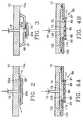
- FIG. 1A is a cross-sectional view of the ceiling of a plasma reactor including a first embodiment of a gas distribution slotted nozzle of the present invention.
- FIG. 1B is a cross-sectional view of the ceiling of a plasma reactor including a second embodiment of a gas distribution slotted nozzle of the present invention.
- FIG. 1C is a cross-sectional view of the ceiling of a plasma reactor including a third embodiment of a gas distribution slotted nozzle of the present invention.
- FIG. 1D is a cross-sectional view of an embodiment corresponding to FIG. 1C but having a vertical slotted nozzle.
- FIG. 2 is a cross-sectional view of the ceiling of a plasma reactor including a fourth embodiment of a gas distribution slotted nozzle of the present invention.
- FIG. 3 is a cross-sectional view of the ceiling of a plasma reactor including a fifth embodiment of a gas distribution slotted nozzle of the present invention.
- FIG. 4A is a cross-sectional view of the ceiling of a plasma reactor including a sixth embodiment of a gas distribution slotted nozzle of the present invention.
- FIG. 4B is a cross-sectional view of an embodiment corresponding to FIG. 4A but having vertical slotted nozzles.
- FIG. 5 is a perspective exploded view of a portion of the gas distribution slotted nozzle of FIG. 4A.
- FIG. 6A is a cross-sectional view of the ceiling of a plasma reactor including a seventh embodiment of a gas distribution slotted nozzle of the present invention.
- FIG. 6B is cross-sectional view of an embodiment corresponding to FIG. 6A but having vertical slotted apertures.
- FIG. 7A is an enlarged cross-sectional view of a top-inserted version of a single slot "in-lid" embodiment of the invention corresponding to FIG. 1C.
- FIG. 7B is an enlarged cross-sectional view of a top-inserted version of a single slot "in-lid" embodiment of the invention corresponding to FIG. 1D.
- FIG. 7C is a cross-sectional view of a two-slit version of the embodiment of FIG. 7A.
- FIG. 7D is a cross-sectional view of a two-slit version of the embodiment of FIG. 7B.
- FIG. 7E is a cross-sectional view of a three-slit version of the embodiment of FIG. 7C.
- FIG. 7F is a cross-sectional view of a three-slit version of the embodiment of FIG. 7D.
- FIG. 7G is a perspective view of a central disk of the blocking plate assembly in the embodiment of FIG. 7D.
- FIG. 8 is a cross-sectional view of nearly an entire plasma reactor in which the embodiment of FIG. 7A is installed.
- FIG. 9 is a graph illustrating etch rate uniformity across the wafer surface as a function of the diameter of the gas distribution slotted nozzle of FIG. 7B.
- FIG. 10 is a graph illustrating the effect on etch rate uniformity across the wafer surface of the combination of plural slotted nozzles of different diameters.
- FIG. 11 is a graph comparing etch rates across the wafer surface with the focus ring (white square curve) and without the focus ring (black square curve).
- FIG. 12 is a bottom view of a circular slotted nozzle in accordance with one aspect of the invention.
- FIG. 13 is a bottom view of a slotted nozzle in accordance with a further aspect of the invention consisting of plural discrete arcuate sections.
- FIG. 14 is a bottom view of a slotted nozzle in accordance with a yet further aspect of the invention having a meandering curved shape divisible into plural arcuate sections.
- FIG. 15 illustrates how the slotted nozzle of FIG. 14 may be segmented and how the segments may be oriented relative to external magnets of an ER-RIE plasma reactor.
- The invention replaces the conventional flat gas distribution plate (i.e., a showerhead or perforated plate) having plural gas injection orifices therethrough near the chamber ceiling. The invention is a gas distribution apparatus in or on the chamber lid or ceiling. In a first embodiment of the invention illustrated in FIG. 1A, the reactor chamber top wall or
lid 10 has agas injection passage 15 therethrough. A disk-shapedblocking plate 20a suspended and spaced from thelid 10 forms a circular slotted aperture ornozzle 25 between acircular ridge 20a' of the blockingplate 20a and theceiling surface 10a of thechamber lid 10. In general, the blockingplate 20a is a solid symmetrical element having its axis of symmetry approximately centered with respect to theinjection passage 15 so as to uniformly disperse the gas flowing from theinjection passage 15. The blockingplate 20a is sufficiently close to thelid 10 so that theaperture 25 is a long thin and preferably continuous opening. A symmetricalannular reflector 35a attached to theceiling surface 10a is centered relative to and surrounds theplate 20a so as to focus the gas injected through thecircular aperture 25 toward the center of the chamber in order to enhance the etch rate near the wafer center. - In a second embodiment illustrated in FIG. 1B, the size of the entire gas injection apparatus is reduced by employing the disk-shaped blocking plate 20b of reduced diameter and employing the annular reflector 35b of reduced diameter. In the embodiment of FIG. 1A, the
annular reflector 35a has aninner surface 36a disposed at an obtuse angle relative to the blockingplate 20a, while in the embodiment of FIG. 1B the annular reflector 35b has an inner surface 36b disposed at an acute angle relative to the blockingplate 20 for greater focusing of the injected gases toward the wafer center. In the embodiments of FIGS. 1A and 1B, thegas injection port 15 is centered with respect to the chamber andlid 10. - A third embodiment of the invention is illustrated in FIG. 1C. In this embodiment, the entire gas injection apparatus is contained within the
lid 10 and consists of agas passage liner 40 including a cylindricalupper liner 42 forming a cylindricaltop passage 43, an annularintermediate liner 44 extending radially outwardly from the base of the cylindricalupper liner 42, and an inverted truncated conical annularbottom liner 46 extending from the edge periphery of the annularintermediate liner 44 to theceiling surface 10a of thelid 10. An inverted truncatedconical center disk 50 is fastened in place in the interior space surrounded by thebottom liner 46 and is congruent therewith. Thedisk 50 is spaced from theintermediate liner 44 to form a horizontal flat disk-shapedgas manifold 55. Furthermore, thedisk 50 is spaced from thebottom liner 46 to form a conical annular shaped slottedaperture 60 which serves as the gas injection nozzle. The conical angle at which the slottedaperture 60 is disposed does not necessarily have to be the angle depicted in FIG. 1C. It is selected to provide an optimum uniform distribution of etch rate across the wafer surface. For example, the angle can be selected to bias the gas distribution toward the center of the wafer to compensate for the usual tendency of plasma etch processes to have a lower etch rate at the center of the wafer. Overall, process conditions and hardware parameters in addition to the nozzle design impact etch rate uniformity, so the slottedaperture 60 can be vertical (as in the embodiment of FIG. 1D referenced below) or angled inwardly or angled outwardly with respect to its central axis. - FIG. 1D illustrates a fourth embodiment, which is identical to the embodiment of FIG. 1C except that the slotted aperture is vertical and the annular
bottom liner 46 andcenter disk 50 are cylindrical rather than conical. FIG. 1D is a preferred embodiment. - An advantage of the invention is that the interior surfaces of the nozzle passages, including the interior surfaces of the manifold 55 and the interior surface of the slotted aperture or
nozzle 60, are free of surface defects and therefore are not subject to corrosion or erosion. This is because theliner 40, including itsconstituent elements center disk 50 are manufactured and machined as separate pieces prior to assembly of the gas distribution apparatus. Thus, the interior surfaces are, during manufacturing, exterior surfaces of the separate pieces 40 (including 42, 44, 46) and 50. Accordingly, external polishing procedures are employed to achieve a defect-free smooth surface on each piece. This solves one aspect of the problem of contamination from erosion or corrosion of gas passage internal surfaces. - Another advantage of the invention is the small size or diameter of the gas distribution apparatus relative to the wafer diameter, particularly in the case of the preferred embodiment of FIG. 1D. Because of its small radial extent, the gas distribution apparatus, including the
liner 40 and thecenter disk 50, need not be formed of a conductor material. As long as thelid 10 is a conductor, it is not necessary that the small gas distribution apparatus of FIG. 1D be a conductor to provide a ground plane at the top of the chamber. Therefore, it is preferable that the gas distribution apparatus including theliner 40 and thecenter disk 50 be formed of a material impervious to attack by the plasma or etchant species in the gas injected into the plasma. A preferred material is ceramic or an insulator such as quartz. As a result, the gases to be injected (such as chlorine or boron trichloride in the case of an etch reactor) never contact aluminum on their way into the reactor chamber. Specifically, thegas feed line 65 to thecylindrical injection passage 43 is stainless steel, so that the injected gases contact either the steel material of thegas feed line 65 or the quartz or ceramic material of theliner 40 andcenter disk 50. The foregoing features, including the external polishing of theliner 40 andcenter disk 50 surfaces and the use of materials such as ceramic or quartz, eliminate the problem of contamination due to corrosion and erosion of gas distribution materials. - FIG. 2 illustrates an embodiment corresponding to FIG. 1A, but without the
reflector 35a. The embodiment of FIG. 2 was found to provide a deviation in metal etch rate uniformity across a 200 mm diameter wafer surface not exceeding about 20%, uniformity being defined herein as [(max-min)/2*average]. - FIG. 3 illustrates a modification of the embodiment of FIG. 2 in which a disk-shaped injection
manifold floor 67 having acenter gas outlet 67a therethrough is attached to the bottom of thelid 10 by a truncatedconical annulus 68. The blocking plate 20b (from FIG. 1B) faces the bottom of the gas outlet so as to uniformly disperse gases emanating from thegas outlet 67. The embodiment of FIG. 3 was found to provide a deviation in metal etch uniformity across the wafer surface not exceeding about 9%. - FIG. 4A illustrates another preferred embodiment of the invention having a blocking
plate assembly 69 consisting of aparallelogramic annulus 70 and a smaller truncated conical center disk 75 (similar to thecenter disk 50 of FIG. 1C) within theannulus 70, and anouter annulus 77, forming two concentric circular slotted inwardly-angled apertures ornozzles apertures annuli plate assembly 69 of FIG. 4A prior to assembly at a point at which all of the interior gas nozzle passages are exterior surfaces of theseparate pieces separate pieces radial spokes 96, theouter piece 77 being fastened bybolts lid 10, as will now be described. For this purpose, aninjection manifold floor 100 is attached to thelid 10 about anopening 110 through the lid providing access to thepassages ceiling 120 in thelid 10 and the injectionmanifold floor 100 form agas injection manifold 125 over thepassages bolts floor 100. - FIG. 6A illustrates an expansion of the concept of FIG. 4A in which the blocking
plate assembly 69 is modified to include a pair of concentric parallelogramic annuli 72, 74, providing three circular slotted apertures ornozzles floor 100. FIG. 6B illustrates an embodiment corresponding to FIG. 6A but having vertical slottedapertures - FIG. 7A is an enlarged view of an embodiment which, like that of FIG. 1C, has a single slotted
aperture 60, and is contained entirely within thelid 10, thereby eliminating any need for an attached floor (such as thefloor 100 of FIG. 4A) and presenting a flush surface toward the interior of the reactor chamber, a significant advantage. The embodiment of FIG. 7A is a modular self-aligning assembly and requires fewer parts. Each element of the assembly is polished prior to assembly. Also, theliner element 46 is supported by aledge 91 machined around an opening through thelid 10, which allows installation without removing thelid 10, makes sealing easier, and can more easily accommodate the pressure differential between ambient and the vacuum chamber. Furthermore, the embodiment of FIG. 7A requires no fasteners on the chamber side of the sealing surfaces. A significant advantage is that the modular construction of the gas distribution apparatus of FIG. 7A requires no drilling of gas passage holes, even though it succeeds in providing gas flow nozzles or slotted apertures with a width less than the plasma sheath thickness. In the absence of any necessity of drilling small holes, crystalline materials such as quartz or sapphire may be employed, if desired. Such crystalline materials, if chosen, are highly suitable in corrosive gas environments. - FIG. 7A shows how the gas distribution apparatus is bolted with an
exterior mounting ring 137 to thelid 10 and how O-ring seals 140 are employed to block gas flow along undesirable paths. The slottedaperture 60 is between about 20-30 mils wide. FIG. 7B is an enlarged view of one implementation of the embodiment of FIG. 7A, having a vertical gas exit flow (slotted aperture 60). FIG. 7B is also a preferred embodiment. - FIG. 7C is a cross-sectional view of a two-slit version of the embodiment of FIG. 7A and employs the truncated
conical center disk 75 and truncatedconical annulus 70 of FIG. 4A to form the two slottedapertures - FIG. 7D is a cross-sectional view of a two-slit version of the embodiment of FIG. 7B, in which the
disk 75 andannular member 70 are cylindrical and are each contained within thelid 10, the inner and outer slottedapertures annulus outer ring 145 surrounds the outer slottedaperture 85. Theannular member 70 of FIG. 7D comprises a pair ofannular members 70a, 70b. In a preferred implementation, the pair ofannular members 70, 70b may be formed as a single integral member, eliminating the seal between them. In the embodiment of FIG. 7D, theouter ring 145 is L-shaped so that it rests on theledge 91. The annulus 70 (70b) has plural circumferentially spacedears 150 extending radially outwardly from its outer circumference and nesting in a ledge in the inner circumference of theouter ring 145, theears 150 there supporting theannulus 70. Theears 150 on the annulus transfer the weight of theannulus 70 to theouter ring 145. Likewise, thecenter disk 75 is supported by plural circumferentially spacedears 150 extending from its outer circumference and nesting inslots 155 in theannulus 70. The spacedears 150 form gaps 165 (illustrated in FIG. 7G) therebetween so that theears 150 do not prevent gas flow through thegas flow passages ears 150 nesting inslots 155 described here with reference to FIG. 7D is also employed in the embodiment of FIG. 7B.) Conventional O-rings 140 provide seals to restrict gas flow to the slottedapertures gas manifold 170 formed between the mountingring 137 and the top surfaces of the gas distribution hardware receives gas from the gasinlet supply passage 275, the gas flowing out of the manifold 170 through the slottedapertures annular members 70a, 70b, thedisk 75 and theouter ring 145 may be polyimide but are preferably ceramic and about 1.2 cm thick. Thelid 10 was formed of aluminum anodized on the bottom surface facing the reactor chamber. In general, the structure defining the slotted apertures, including theannular members 70,disk 75 andring 145 may be formed of any of the following materials: ceramic, quartz, sapphire, polyimide and anodized aluminum. The flange or mountingring 137 was formed of stainless steel and the O-rings 140 were of a conventional type suitable for use with corrosive gases. The combination of stainlesssteel mounting ring 137/supply passage 275 and ceramic or quartz slottedapertures apertures - FIG. 7E illustrates a three-slot version of the embodiment of FIG. 7C and is identical in most respects with the exception of the replacement of the
annular member 70 with the inner and outerannular members annular members 70a, 70b with the inner and outerannular members annular members annular members 74a, 74b may be combined as a single integral member. - The embodiment of FIG. 7B has been tested in a production environment. Approximately 12,000 six-inch diameter wafers were processed using a ceramic version of the embodiment of FIG. 7B, after which the plasma reactor chamber showed no signs of significant particle contamination increase, particle contamination levels remaining within acceptable process limits. Visual inspection of the slit nozzle parts showed no signs of degradation or wear due to exposure to the corrosive etch chemistry. Furthermore, the anodized chamber side of the lid surrounding the slit nozzle showed no signs of wear or corrosion. In comparison, for chambers equipped with a conventional gas distribution plate, the gas distribution plate typically shows enough wear or degradation to require replacement after processing of only 5,000 wafers. This comparison demonstrates the longer life and lower cost of consumable materials realized in the present invention relative to conventional gas distribution plates currently employed in typical plasma reactor chambers.
- FIG. 8 illustrates a plasma reactor having the gas distribution apparatus of FIG. 7A. The
lid 10 is part of acylindrical chamber housing 200 containing awafer pedestal 210 supporting asemiconductor wafer 220 which is to be processed. AnRF coil antenna 230 wrapped around thereactor chamber housing 200 is powered by a matchedRF source 240, constituting the plasma source power. A biasRF power source 250 controlling the ion bombardment energy is connected to thewafer pedestal 210. However, other RF power source configurations may be employed. For example, a magnetically enhanced reactive ion etch apparatus can be employed in which the RF antenna coil and RF source are replaced with electromagnetic coils and the RF power is input only to thewafer pedestal 210. Avacuum pump 260 and throttle valve (not shown) control the chamber interior gas pressure. Agas supply 270 is connected through asteel inlet tube 275 to thegas distribution manifold 55 of the gas distribution apparatus. - FIG. 9 illustrates how the diameter of the slotted
aperture nozzle 60 of FIG. 7B can be varied to select a desired etch rate distribution across a 150 mm diameter wafer. FIG. 9 shows the average etch rate as a function of radial position normalized to the etch rate at the center of the wafer. The etch rate at the middle and edge increases relative to the center as the diameter of the slotted nozzle is increased from 2.5 cm (dotted line curve) to 3.3 cm (dashed line curve) and then to 3.7 cm (solid line curve). In an implementation corresponding to FIG. 6B but with a single circular slit, increasing the nozzle diameter from 1.8 cm, to 2.5 cm and then to 3.1 cm provided respective deviations in etch rate uniformity across the wafer diameter of 24%, 12% and 8%, respectively. - FIG. 10 illustrates the etch rate distribution across a 200 mm diameter wafer for a double slit configuration. The data in FIG. 10 correspond to the embodiment of FIG. 7D. The
slits - Referring again to FIG. 8, in order to decrease or control the etch rate near the wafer periphery, a
focus ring 278 may be added surrounding the wafer periphery. The focus ring reduces the flow of etchant species across the chemical boundary separating the plasma region over the wafer center having a scarcity of etchant species ions and the plasma region beyond the wafer periphery having a plentitude of etchant species ions. FIG. 11 illustrates how the addition of the focus ring reduces the etch rate near the periphery of a 200 mm diameter wafer from a high rate of about 860 nm/min (black square curve) to a low rate of about 720 nm/min (white square curve). The fact that the focus ring strongly modulates the etch rate at the wafer periphery implies that etch rate variation across the wafer can be minimized by judicious selection of nozzle diameter(s) combined with focus ring height. - Overall, etch rate uniformity comparable to that achieved with conventional gas distribution plates has been demonstrated with the present invention, while providing far greater advantages in resistance to corrosion. As mentioned hereinabove, conventional gas distribution plate are typically designed with more orifices per unit area over the wafer center to enhance the etch rate at the wafer center. An advantage of the present invention is that, despite having a very small number of slotted aperture nozzles (compared to the large number of small orifices in a conventional gas distribution plate), it inherently delivers sufficient gas over the center of the wafer to achieve the same etch rate uniformity.
- FIG. 12 is a bottom view of the circular slotted
aperture nozzle 60 of FIG. 1C. FIG. 13 illustrates how thenozzle 60 may be segmented into discretearcuate sub-sections 60a-60d, while FIG 14 illustrates how thenozzle 60 can follow a meanderingarcuate path 140 having aportion 150 thereof deleted, rather than a circular path. FIG. 15 illustrates how the embodiment of FIG. 14 can be segmented into separate arcuate sub-sections. The embodiments of FIGS. 13-15 could be useful for applications in magnetically enhanced reactive ion etch (ME-RIE) reactors in which the corners between adjacent external magnets of the reactor have somewhat higher magnetic fields and therefore higher etch rates with a uniform etchant gas distribution. This non-uniformity can be compensated by aligning the gaps betweenadjacent sections 60a-60d of the slottedaperture nozzle 60 over the regions of high magnetic field density. In the case of an ME-RIE plasma reactor, such an alignment is shown in FIG. 15 by indicating in dashed line the relative orientation of the four external magnets 200a-200d of the reactor with reference to the fourdiscrete nozzle sections 60a-60d. It is currently felt that such fine tuning of etch rate uniformity is not necessary. - In the embodiments of FIGS. 1C, 1D, 7A and 7B employing a single slotted
aperture 60, the aperture diameter is generally in the broad range of 0.5 inches (1.2 cm) to 6.0 inches (15 cm), although the preferred range is 1.0 inches (2.5 cm) to 2.0 inches (5.0 cm). In the embodiments of FIGS. 4A, 4B, 7C and 7D employing a pair of slottedapertures apertures - The invention provides a combination of advantages over conventional gas distribution plates. Because it is a modular assembly with separate pieces forming elongate apertures or nozzles with a gap not exceeding the plasma sheath thickness, the separate pieces are polished externally so that no surface imperfections can contribute to degradation or particle contamination in a corrosive gas environment. Moreover, the absence of any drilled holes permits the use of any corrosive-resistant materials including quartz or sapphire as well as ceramics, which, in combination with a stainless steel gas inlet, provides a gas distribution apparatus virtually impervious to attack from corrosive gases. The modular design provides drop-in self-aligning assembly for ease of manufacture. Despite the small number of nozzles compared with conventional gas distribution plates, the invention achieves comparable etch rate uniformity and design versatility while at the same time providing cycle lifetime many times that of conventional gas distribution plates. This in turn provides greater throughput by reducing frequency of production down-time for replacing consumable materials.
- While the invention has been described in detail by specific reference to preferred embodiments thereof, it is understood that variations and modifications thereof may be made without departing from the true spirit and scope of the invention.
Claims (81)
- A plasma reactor comprising:
a reactor vacuum chamber having a chamber housing;
a pedestal holding a workpiece to be processed;
means for applying RF energy into said chamber;
gas injection apparatus, comprising:
a gas supply containing a processing species in a gas,
an opening in said chamber housing,
a gas feed line from said supply to said opening in said chamber housing,
gas distribution apparatus near said opening in said chamber housing, said gas feed apparatus having at least one elongate thin slit nozzle facing the interior of said chamber. - The reactor of Claim 1 wherein said gas distribution apparatus comprises:
a disk member surrounded by at least one annular member with a gap therebetween comprising said slit nozzle, said disk member and annular member dispersing gas flow from said opening in said chamber housing to said slit nozzle. - The reactor of Claim 2 wherein said gas distribution apparatus is contained within said opening in said chamber housing.
- The reactor of Claim 2 wherein said gas distribution apparatus is suspended inside said chamber adjacent said opening in said chamber housing.
- The reactor of Claim 2 further comprising an intermediate annular member surrounding said annular member and separated therefrom by a gap therebetween comprising an intermediate slit nozzle.
- The reactor of Claim 5 further comprising an outer annular member surrounding said intermediate annular member and separated therefrom by a gap therebetween comprising an outer slit nozzle.
- The reactor of Claim 2 wherein said disk member and said annular member are cylindrical and concentric with one another.
- The reactor of Claim 2 wherein said disk member and said annular member are each mutually congruent truncated conical sections.
- The reactor of Claim 8 wherein said conical sections correspond to a cone whose apex faces toward the center of said workpiece, whereby each slit nozzle directs gas flowing therethrough toward said center of said workpiece.
- The reactor of Claim 5 wherein said disk member and said annular member are each mutually congruent truncated conical sections.
- The reactor of Claim 10 wherein said conical sections correspond to a cone whose apex faces toward the center of said workpiece, whereby each slit nozzle directs gas flowing therethrough toward said center of said workpiece.
- The reactor of Claim 2 wherein each of said members of said gas distribution apparatus comprises a material at least nearly impervious to attack from said etchant species.
- The reactor of Claim 12 wherein said etchant species comprises at least one of (a) chlorine and (b) boron tri-chloride.
- The reactor of Claim 12 wherein said material at least nearly impervious to attack from said etchant species comprises one of: (a) ceramic, (b) quartz, (c) sapphire, (d) polyimide, (e) anodized aluminum.
- The reactor of Claim 1 further comprising a focus ring adjacent said pedestal surrounding a peripheral edge of said workpiece.
- The reactor of Claim 12 wherein said gas feed line comprises stainless steel and wherein each of said members of said gas distribution apparatus comprises one of: (a) ceramic, (b) quartz, (c) sapphire, (d) polyimide, (e) anodized aluminum.
- The reactor of Claim 2 wherein each of said members has its surface polished prior to assembly of said gas distribution apparatus.
- The reactor of Claim 2 wherein said slit nozzle follows a closed circular path.
- The reactor of Claim 18 wherein said closed circular path is segmented so as to reduce gas flow over selected portions of said workpiece.
- The reactor of Claim 2 wherein said slit nozzle follows a meandering arcuate path.
- The reactor of Claim 20 wherein said meandering arcuate path is segmented.
- The reactor of Claim 1 wherein said chamber housing comprises a lid overlying said workpiece and having a ceiling surface thereof facing said workpiece, and wherein said opening through said chamber housing is in said lid.
- The reactor of Claim 1 wherein said gas distribution apparatus comprises a blocking plate in said chamber facing said opening through said chamber housing and separated from said chamber housing by a gap along a peripheral edge of said blocking plate, said gap comprising said slot nozzle.
- The reactor of Claim 23 further comprising an annular gas reflector surrounding said blocking plate.
- The reactor of Claim 24 wherein said gas reflector comprises a reflector surface facing and acutely oriented relative to said blocking plate.
- The reactor of Claim 24 wherein said gas reflector comprises a reflector surface facing and obliquely oriented relative to said blocking plate.
- The reactor of Claim 1 wherein said slit nozzle has a diameter generally in the range of 0.5 inches (1.2 cm) to 6.0 inches (15 cm).
- The reactor of Claim 27 wherein said slit nozzle has a diameter in the range of 1.0 inches (2.5 cm) to 2.0 inches (5.0 cm).
- The reactor of Claim 5 wherein said intermediate slit nozzle has a diameter in the range of 3.0 inches (7.5 cm) to 6.0 inches (15 cm) and said slit nozzle has a diameter generally in the range of 0.5 inches (1.2 cm) to 2.0 inches (5.0 cm).
- The reactor of Claim 29 wherein said intermediate slit nozzle and said slit nozzle have diameters generally on the order to about 4.0 inches (10 cm) and about 1.5 inches (3.7 cm), respectively.
- The reactor of Claim 6 wherein said slit nozzle, said intermediate slit nozzle and said outer slit nozzle have diameters on the order of about one of:(a) 0.3 inch (0.8 cm), 1.0 inch (2.5 cm) and 1.25 inches (3.0 cm), respectively, and(b) 4 inches (10 cm), 2.5 inches (6.3 cm) and 1 inch (2.5 cm), respectively.
- A gas injection apparatus for injecting gases into a plasma reactor vacuum chamber having a chamber housing, a pedestal holding a workpiece to be processed, means for applying RF energy into said chamber, said gas injection apparatus comprising:
a gas supply containing an etchant species in a gas,
an opening in said chamber housing, a gas feed line from said supply to said opening in said chamber housing,
gas distribution apparatus near said opening in said chamber housing, said gas feed apparatus having at least one slit nozzle facing the interior of said chamber. - The reactor of Claim 32 wherein said gas distribution apparatus comprises:
a disk member surrounded by at least one annular member with a gap therebetween comprising said slit nozzle, said disk member and annular member blocking gas flow through said opening in said chamber housing. - The reactor of Claim 33 wherein said gas distribution apparatus is contained within said opening in said chamber housing.
- The reactor of Claim 33 wherein said gas distribution apparatus is suspended inside said chamber adjacent said opening in said chamber housing.
- The reactor of Claim 33 further comprising an intermediate annular member surrounding said annular member and separated therefrom by a gap therebetween comprising an intermediate slit nozzle.
- The reactor of Claim 36 further comprising an outer annular member surrounding said intermediate annular member and separated therefrom by a gap therebetween comprising an outer slit nozzle.
- The reactor of Claim 33 wherein said disk member and said annular member are cylindrical and concentric with one another.
- The reactor of Claim 33 wherein said disk member and said annular member are each mutually congruent truncated conical sections.
- The reactor of Claim 39 wherein said conical sections correspond to a cone whose apex faces toward the center of said workpiece, whereby each slit nozzle directs gas flowing therethrough toward said center of said workpiece.
- The reactor of Claim 36 wherein said disk member and said annular member are each mutually congruent truncated conical sections.
- The reactor of Claim 41 wherein said conical sections correspond to a cone whose apex faces toward the center of said workpiece, whereby each slit nozzle directs gas flowing therethrough toward said center of said workpiece.
- The reactor of Claim 33 wherein each of said members of said gas distribution apparatus comprises a material at least nearly impervious to attack from said etchant species.
- The reactor of Claim 43 wherein said etchant species comprises at least one of (a) chlorine and (b) boron tri-chloride.
- The reactor of Claim 43 wherein said material at least nearly impervious to attack from said etchant species comprises one of: (a) ceramic, (b) quartz, (c) sapphire, (d) polyimide, (e) anodized aluminum.
- The reactor of Claim 32 further comprising a focus ring adjacent said pedestal surrounding a peripheral edge of said workpiece.
- The reactor of Claim 43 wherein said gas feed line comprises stainless steel and wherein each of said members of said gas distribution apparatus comprises one of: (a) ceramic, (b) quartz, (c) sapphire, (d) polyimide, (e) anodized aluminum.
- The reactor of Claim 32 wherein each of said members has its surface polished prior to assembly of said gas distribution apparatus.
- The reactor of Claim 32 wherein said slit nozzle follows a closed circular path.
- The reactor of Claim 49 wherein said closed circular path is segmented so as to reduce gas flow over selected portions of said workpiece.
- The reactor of Claim 32 wherein said slit nozzle follows a meandering arcuate path.
- The reactor of Claim 51 wherein said meandering arcuate path is segmented.
- The reactor of Claim 32 wherein said chamber housing comprises a lid overlying said workpiece and having a ceiling surface thereof facing said workpiece, and wherein said opening through said chamber housing is in said lid.
- The reactor of Claim 32 wherein said gas distribution apparatus comprises a blocking plate in said chamber facing said opening through said chamber housing and separated from said chamber housing by a gap along a peripheral edge of said blocking plate, said gap comprising said slot nozzle.
- The reactor of Claim 54 further comprising an annular gas reflector surrounding said blocking plate.
- The reactor of Claim 55 wherein said gas reflector comprises an acutely oriented reflector surface facing said blocking plate.
- The reactor of Claim 55 wherein said gas reflector comprises an obliquely oriented reflector surface facing said blocking plate.
- The reactor of Claim 32 wherein said slit nozzle has a diameter generally in the range of 0.5 inches (1.2 cm) to 6.0 inches (15 cm).
- The reactor of Claim 58 wherein said slit nozzle has a diameter in the range of 1.0 inches (2.5 cm) to 2.0 inches (5.0 cm).
- The reactor of Claim 36 wherein said intermediate slit nozzle has a diameter in the range of 3.0 inches (7.5 cm) to 6.0 inches (15 cm) and said slit nozzle has a diameter generally in the range of 0.5 inches (1.2 cm) to 2.0 inches (5.0 cm).
- The reactor of Claim 60 wherein said intermediate slit nozzle and said slit nozzle have diameters generally on the order to about 4.0 inches (10 cm) and about 1.5 inches (3.7 cm), respectively.
- The reactor of Claim 37 wherein said slit nozzle, said intermediate slit nozzle and said outer slit nozzle have diameters on the order of about one of:(a) 0.3 inch (0.8 cm), 1.0 inch (2.5 cm) and 1.25 inches (3.0 cm), respectively, and(b) 4 inches (10 cm), 2.5 inches (6.3 cm) and 1 inch (2.5 cm), respectively.
- The reactor of Claim 33 wherein said reactor comprises a lid having a bottom surface facing and enclosing said reactor vacuum chamber, and wherein said disk member and said annular member are both contained within an opening in said lid and have respective bottom surfaces co-planar with the bottom surface of said lid.
- The reactor of Claim 36 wherein said reactor comprises a lid having a bottom surface facing and enclosing said reactor vacuum chamber, and wherein said disk member, said annular member and said intermediate annular member are contained within an opening in said lid and have respective bottom surfaces co-planar with the bottom surface of said lid.
- The reactor of Claim 37 wherein said reactor comprises a lid having a bottom surface facing and enclosing said reactor vacuum chamber, and wherein said disk member, said annular member, said intermediate annular member and said outer annular member are contained within an opening in said lid and have respective bottom surfaces co-planar with the bottom surface of said lid.
- A reactor chamber for use with a source of process gas, comprising:
a pedestal adapted to mount a workpiece to be processed;
an applicator for coupling RF energy into the chamber;
a gas injection device including at least one solid central element adjacent and across the outlet of said channel, said element being closely spaced to adjacent chamber interior elements to define one or more slit passageways centered about a central axis coinciding with that of said channel, and so that said slit passageways may be oriented to direct the process gas into said chamber interior one of (a) generally perpendicularly of said pedestal, (b) angled inwardly and (c) angled outwardly of said central axis. - The chamber of Claim 66, further including a focus ring mounted upon said pedestal and adapted to surround a workpiece to be processed and to extend above the position of said workpiece in a manner related to injection device diameter, whereby to improve process uniformity across said workpiece.
- The plasma reactor of Claim 66, wherein said gas injection device further includes at least one annular ring positioned concentrically with said central element and closely spaced thereto to define said slit passageways.
- The plasma reactor of Claim 66 wherein said gas injection device comprises an insulating material, and said adjacent wall of said chamber comprises a conductive material.
- The plasma reactor of Claim 66 wherein said gas injection device is recessed within the upper wall of said chamber.
- The plasma reactor of Claim 70 wherein said gas injection device further includes at least one annular ring concentrically mounted with said central element and closely spaced thereto to define at least one slit passageway therebetween.
- The plasma reactor of Claim 71 wherein said central element is a disk whose diameter is at least an order of magnitude larger than the diameter of said channel.
- The plasma reactor of Claim 71 wherein said central element is a cylindrical element whose diameter is greater than but of the same order of magnitude as the diameter of said channel.
- The plasma reactor of Claim 70 wherein said gas injection device comprises an insulating material which is generally non-reactive in the plasma environment of the chamber interior.
- The plasma reactor of Claim 66 wherein said slit passageway is a continuous slit.
- The plasma reactor of Claim 75 wherein said slit passage way comprises an array of discrete slits.
- The plasma reactor of Claim 76 wherein said array of discrete slits is symmetrically disposed relative to said central axis.
- A plasma reactor for use with a source of process gas, comprising:
a reactor chamber having an interior capable of being evacuated, and provided with a channel to permit communication between a source of process gas and the interior of said chamber;
a pedestal adapted to mount a workpiece to be processed;
an applicator for coupling RF energy into the interior of said chamber; and
a gas injection device including at least one solid central element adjacent and across the outlet of said channel, said element being surrounded by at least one annular member having a central axis of symmetry with a gap therebetween to define at least one slit passageway directing the gas toward said pedestal, said central and annular elements otherwise blocking gas flow from said channel into said chamber. - The reactor of Claim 78 wherein said slit passageway is oriented to direct the process gas into said chamber interior in a direction generally perpendicular of said pedestal.
- The reactor of Claim 78 wherein said slit passageway is oriented to direct the process gas into said chamber interior in a direction angled inwardly of said central axis.
- The reactor of Claim 78 wherein said slit passageway is oriented to direct the process gas into said chamber interior in a direction angled outwardly of said central axis.
Applications Claiming Priority (2)
| Application Number | Priority Date | Filing Date | Title |
|---|---|---|---|
| US307888 | 1994-09-16 | ||
| US08/307,888US5643394A (en) | 1994-09-16 | 1994-09-16 | Gas injection slit nozzle for a plasma process reactor |
Publications (3)
| Publication Number | Publication Date |
|---|---|
| EP0702392A2true EP0702392A2 (en) | 1996-03-20 |
| EP0702392A3 EP0702392A3 (en) | 1996-04-10 |
| EP0702392B1 EP0702392B1 (en) | 2000-10-04 |
Family
ID=23191595
Family Applications (1)
| Application Number | Title | Priority Date | Filing Date |
|---|---|---|---|
| EP95305793AExpired - LifetimeEP0702392B1 (en) | 1994-09-16 | 1995-08-18 | Plasma reactor |
Country Status (5)
| Country | Link |
|---|---|
| US (1) | US5643394A (en) |
| EP (1) | EP0702392B1 (en) |
| JP (1) | JPH08288266A (en) |
| KR (1) | KR960012360A (en) |
| DE (1) | DE69519008T2 (en) |
Cited By (17)
| Publication number | Priority date | Publication date | Assignee | Title |
|---|---|---|---|---|
| EP0768702A1 (en)* | 1995-10-16 | 1997-04-16 | Applied Materials, Inc. | Gas injection slit nozzle for a plasma process reactor |
| JPH10134997A (en)* | 1996-10-24 | 1998-05-22 | Samsung Electron Co Ltd | Plasma processing apparatus that eliminates discharge due to secondary potential |
| WO1999054908A1 (en)* | 1998-04-23 | 1999-10-28 | Applied Materials, Inc. | Crystalline gas distributor for semiconductor plasma etch chamber |
| WO2001024216A3 (en)* | 1999-09-30 | 2002-09-26 | Lam Res Corp | Pretreated gas distribution plate |
| US6829056B1 (en) | 2003-08-21 | 2004-12-07 | Michael Barnes | Monitoring dimensions of features at different locations in the processing of substrates |
| WO2005112072A3 (en)* | 2004-04-30 | 2006-07-27 | Axcelis Tech Inc | Segmented baffle plate assembly for a plasma processing system |
| WO2006096674A1 (en)* | 2005-03-07 | 2006-09-14 | Applied Materials, Inc. | Gas baffle and distributor for semiconductor processing chamber |
| EP1918970A1 (en)* | 2006-10-30 | 2008-05-07 | Applied Materials, Inc. | Method and apparatus for photomask plasma etching |
| US7510624B2 (en) | 2004-12-17 | 2009-03-31 | Applied Materials, Inc. | Self-cooling gas delivery apparatus under high vacuum for high density plasma applications |
| US7740706B2 (en) | 2006-11-28 | 2010-06-22 | Applied Materials, Inc. | Gas baffle and distributor for semiconductor processing chamber |
| US7758698B2 (en) | 2006-11-28 | 2010-07-20 | Applied Materials, Inc. | Dual top gas feed through distributor for high density plasma chamber |
| US7799704B2 (en) | 2006-11-28 | 2010-09-21 | Applied Materials, Inc. | Gas baffle and distributor for semiconductor processing chamber |
| US7909961B2 (en) | 2006-10-30 | 2011-03-22 | Applied Materials, Inc. | Method and apparatus for photomask plasma etching |
| US8349128B2 (en) | 2004-06-30 | 2013-01-08 | Applied Materials, Inc. | Method and apparatus for stable plasma processing |
| US9129778B2 (en) | 2011-03-18 | 2015-09-08 | Lam Research Corporation | Fluid distribution members and/or assemblies |
| TWI575556B (en)* | 2014-08-22 | 2017-03-21 | Electrolyte processing device | |
| CN114059020A (en)* | 2022-01-07 | 2022-02-18 | 北京航空航天大学 | A device and method for improving gas phase ratio in PS-PVD deposition process |
Families Citing this family (135)
| Publication number | Priority date | Publication date | Assignee | Title |
|---|---|---|---|---|
| JPH0925586A (en)* | 1995-07-11 | 1997-01-28 | Anelva Corp | Substrate processing apparatus and substrate processing method |
| US6342135B1 (en)* | 1995-11-02 | 2002-01-29 | Taiwan Semiconductor Manufacturing Company | Sputter etching chamber with improved uniformity |
| US5885358A (en)* | 1996-07-09 | 1999-03-23 | Applied Materials, Inc. | Gas injection slit nozzle for a plasma process reactor |
| US5900064A (en)* | 1997-05-01 | 1999-05-04 | Applied Materials, Inc. | Plasma process chamber |
| JP3470557B2 (en)* | 1997-06-27 | 2003-11-25 | 株式会社日立製作所 | Plasma processing equipment |
| KR100466867B1 (en)* | 1997-07-03 | 2005-04-19 | 삼성전자주식회사 | Plasma-Enhanced Chemical Vapor Deposition Equipment with Constant Deposition Rate |
| DE59702419D1 (en)* | 1997-07-15 | 2000-11-09 | Unaxis Trading Ag Truebbach | Sputter coating method and apparatus |
| US6165910A (en)* | 1997-12-29 | 2000-12-26 | Lam Research Corporation | Self-aligned contacts for semiconductor device |
| JP4124383B2 (en)* | 1998-04-09 | 2008-07-23 | 財団法人国際科学振興財団 | Shower plate for microwave excited plasma device and microwave excited plasma device |
| US6436253B1 (en)* | 1998-05-20 | 2002-08-20 | Taiwan Semiconductor Manufacturing Company | Sputter etching chamber with improved uniformity |
| KR100519543B1 (en)* | 1998-07-09 | 2005-12-08 | 삼성전자주식회사 | Plasma Etching Device for Semiconductor Device Manufacturing |
| US6335293B1 (en) | 1998-07-13 | 2002-01-01 | Mattson Technology, Inc. | Systems and methods for two-sided etch of a semiconductor substrate |
| US6117401A (en)* | 1998-08-04 | 2000-09-12 | Juvan; Christian | Physico-chemical conversion reactor system with a fluid-flow-field constrictor |
| JP4044218B2 (en)* | 1998-08-28 | 2008-02-06 | 松下電器産業株式会社 | Plasma processing equipment |
| US6074953A (en)* | 1998-08-28 | 2000-06-13 | Micron Technology, Inc. | Dual-source plasma etchers, dual-source plasma etching methods, and methods of forming planar coil dual-source plasma etchers |
| KR100292410B1 (en)* | 1998-09-23 | 2001-06-01 | 윤종용 | Process chamber for reducing particulate contamination for manufacturing semiconductor device |
| US6230651B1 (en)* | 1998-12-30 | 2001-05-15 | Lam Research Corporation | Gas injection system for plasma processing |
| US6320320B1 (en)* | 1999-11-15 | 2001-11-20 | Lam Research Corporation | Method and apparatus for producing uniform process rates |
| US6518705B2 (en)* | 1999-11-15 | 2003-02-11 | Lam Research Corporation | Method and apparatus for producing uniform process rates |
| CN1251293C (en)* | 1999-11-15 | 2006-04-12 | 兰姆研究有限公司 | Materials and gas chemistries for processing systems |
| US6391787B1 (en)* | 2000-10-13 | 2002-05-21 | Lam Research Corporation | Stepped upper electrode for plasma processing uniformity |
| CN1229855C (en)* | 2001-03-28 | 2005-11-30 | 大见忠弘 | Plasma treatment device |
| US6663025B1 (en)* | 2001-03-29 | 2003-12-16 | Lam Research Corporation | Diffuser and rapid cycle chamber |
| KR100408405B1 (en)* | 2001-05-03 | 2003-12-06 | 삼성전자주식회사 | Manufacturing apparatus for semiconductor device |
| WO2003003414A2 (en)* | 2001-06-29 | 2003-01-09 | Tokyo Electron Limited | Directed gas injection apparatus for semiconductor processing |
| TWI224815B (en)* | 2001-08-01 | 2004-12-01 | Tokyo Electron Ltd | Gas processing apparatus and gas processing method |
| US20030070620A1 (en) | 2001-10-15 | 2003-04-17 | Cooperberg David J. | Tunable multi-zone gas injection system |
| US7371467B2 (en)* | 2002-01-08 | 2008-05-13 | Applied Materials, Inc. | Process chamber component having electroplated yttrium containing coating |
| US20030192645A1 (en)* | 2002-04-16 | 2003-10-16 | Applied Materials, Inc. | Method and apparatus for creating circumferential process gas flow in a semiconductor wafer plasma reactor chamber |
| US6861094B2 (en)* | 2002-04-25 | 2005-03-01 | Micron Technology, Inc. | Methods for forming thin layers of materials on micro-device workpieces |
| CN100442429C (en)* | 2002-05-23 | 2008-12-10 | 蓝姆研究公司 | Multipart electrode for semiconductor processing plasma reactor and method of replacing a part of multipart electrode |
| US6838114B2 (en) | 2002-05-24 | 2005-01-04 | Micron Technology, Inc. | Methods for controlling gas pulsing in processes for depositing materials onto micro-device workpieces |
| US7118783B2 (en)* | 2002-06-26 | 2006-10-10 | Micron Technology, Inc. | Methods and apparatus for vapor processing of micro-device workpieces |
| US6821347B2 (en)* | 2002-07-08 | 2004-11-23 | Micron Technology, Inc. | Apparatus and method for depositing materials onto microelectronic workpieces |
| US20040011464A1 (en)* | 2002-07-16 | 2004-01-22 | Applied Materials, Inc. | Promotion of independence between degree of dissociation of reactive gas and the amount of ionization of dilutant gas via diverse gas injection |
| JP2005536042A (en)* | 2002-08-08 | 2005-11-24 | トリコン テクノロジーズ リミティド | Improved shower head |
| US6955725B2 (en) | 2002-08-15 | 2005-10-18 | Micron Technology, Inc. | Reactors with isolated gas connectors and methods for depositing materials onto micro-device workpieces |
| US7270713B2 (en)* | 2003-01-07 | 2007-09-18 | Applied Materials, Inc. | Tunable gas distribution plate assembly |
| US6942753B2 (en)* | 2003-04-16 | 2005-09-13 | Applied Materials, Inc. | Gas distribution plate assembly for large area plasma enhanced chemical vapor deposition |
| US7335396B2 (en) | 2003-04-24 | 2008-02-26 | Micron Technology, Inc. | Methods for controlling mass flow rates and pressures in passageways coupled to reaction chambers and systems for depositing material onto microfeature workpieces in reaction chambers |
| US7344755B2 (en) | 2003-08-21 | 2008-03-18 | Micron Technology, Inc. | Methods and apparatus for processing microfeature workpieces; methods for conditioning ALD reaction chambers |
| US7235138B2 (en) | 2003-08-21 | 2007-06-26 | Micron Technology, Inc. | Microfeature workpiece processing apparatus and methods for batch deposition of materials on microfeature workpieces |
| US7422635B2 (en) | 2003-08-28 | 2008-09-09 | Micron Technology, Inc. | Methods and apparatus for processing microfeature workpieces, e.g., for depositing materials on microfeature workpieces |
| US7056806B2 (en) | 2003-09-17 | 2006-06-06 | Micron Technology, Inc. | Microfeature workpiece processing apparatus and methods for controlling deposition of materials on microfeature workpieces |
| US7282239B2 (en) | 2003-09-18 | 2007-10-16 | Micron Technology, Inc. | Systems and methods for depositing material onto microfeature workpieces in reaction chambers |
| US7323231B2 (en) | 2003-10-09 | 2008-01-29 | Micron Technology, Inc. | Apparatus and methods for plasma vapor deposition processes |
| US7581511B2 (en) | 2003-10-10 | 2009-09-01 | Micron Technology, Inc. | Apparatus and methods for manufacturing microfeatures on workpieces using plasma vapor processes |
| US7647886B2 (en) | 2003-10-15 | 2010-01-19 | Micron Technology, Inc. | Systems for depositing material onto workpieces in reaction chambers and methods for removing byproducts from reaction chambers |
| US20050092245A1 (en)* | 2003-11-03 | 2005-05-05 | Ahn-Sik Moon | Plasma chemical vapor deposition apparatus having an improved nozzle configuration |
| JP4273932B2 (en)* | 2003-11-07 | 2009-06-03 | 株式会社島津製作所 | Surface wave excitation plasma CVD equipment |
| US7258892B2 (en) | 2003-12-10 | 2007-08-21 | Micron Technology, Inc. | Methods and systems for controlling temperature during microfeature workpiece processing, e.g., CVD deposition |
| US7892357B2 (en)* | 2004-01-12 | 2011-02-22 | Axcelis Technologies, Inc. | Gas distribution plate assembly for plasma reactors |
| KR101025323B1 (en)* | 2004-01-13 | 2011-03-29 | 가부시키가이샤 아루박 | Etching Apparatus and Etching Method |
| US7906393B2 (en)* | 2004-01-28 | 2011-03-15 | Micron Technology, Inc. | Methods for forming small-scale capacitor structures |
| US7584942B2 (en)* | 2004-03-31 | 2009-09-08 | Micron Technology, Inc. | Ampoules for producing a reaction gas and systems for depositing materials onto microfeature workpieces in reaction chambers |
| US8133554B2 (en) | 2004-05-06 | 2012-03-13 | Micron Technology, Inc. | Methods for depositing material onto microfeature workpieces in reaction chambers and systems for depositing materials onto microfeature workpieces |
| US7699932B2 (en) | 2004-06-02 | 2010-04-20 | Micron Technology, Inc. | Reactors, systems and methods for depositing thin films onto microfeature workpieces |
| US20060021703A1 (en)* | 2004-07-29 | 2006-02-02 | Applied Materials, Inc. | Dual gas faceplate for a showerhead in a semiconductor wafer processing system |
| US8298336B2 (en)* | 2005-04-01 | 2012-10-30 | Lam Research Corporation | High strip rate downstream chamber |
| TWI332532B (en)* | 2005-11-04 | 2010-11-01 | Applied Materials Inc | Apparatus and process for plasma-enhanced atomic layer deposition |
| US7743731B2 (en)* | 2006-03-30 | 2010-06-29 | Tokyo Electron Limited | Reduced contaminant gas injection system and method of using |
| TWI335450B (en)* | 2006-05-15 | 2011-01-01 | Ind Tech Res Inst | Film cleaning method and apparatus |
| KR20080023172A (en)* | 2006-09-08 | 2008-03-12 | 주성엔지니어링(주) | Board Edge Etching Device |
| US7476291B2 (en)* | 2006-09-28 | 2009-01-13 | Lam Research Corporation | High chamber temperature process and chamber design for photo-resist stripping and post-metal etch passivation |
| JP2008124424A (en)* | 2006-10-16 | 2008-05-29 | Tokyo Electron Ltd | Plasma film forming apparatus and plasma film forming method |
| KR101359402B1 (en)* | 2006-10-30 | 2014-02-07 | 주성엔지니어링(주) | Etching Apparatus for edges of substrate |
| JPWO2008156031A1 (en)* | 2007-06-19 | 2010-08-26 | 東京エレクトロン株式会社 | Vacuum processing equipment |
| JP4931716B2 (en)* | 2007-07-18 | 2012-05-16 | 東京エレクトロン株式会社 | Plasma processing apparatus and plasma generation chamber |
| US8673080B2 (en) | 2007-10-16 | 2014-03-18 | Novellus Systems, Inc. | Temperature controlled showerhead |
| US8137463B2 (en)* | 2007-12-19 | 2012-03-20 | Applied Materials, Inc. | Dual zone gas injection nozzle |
| JP5230225B2 (en)* | 2008-03-06 | 2013-07-10 | 東京エレクトロン株式会社 | Lid parts, processing gas diffusion supply device, and substrate processing device |
| KR101404010B1 (en) | 2008-03-06 | 2014-06-12 | 주성엔지니어링(주) | Substrate edge etching apparatus and substrate edge etching method using the same |
| JP4956469B2 (en)* | 2008-03-24 | 2012-06-20 | 株式会社ニューフレアテクノロジー | Semiconductor manufacturing equipment |
| JP4731580B2 (en)* | 2008-03-27 | 2011-07-27 | 東京エレクトロン株式会社 | Film forming method and film forming apparatus |
| US8252114B2 (en)* | 2008-03-28 | 2012-08-28 | Tokyo Electron Limited | Gas distribution system and method for distributing process gas in a processing system |
| JP5665265B2 (en)* | 2008-06-24 | 2015-02-04 | 東京エレクトロン株式会社 | Method and system for introducing process fluid through chamber components |
| US8800484B2 (en)* | 2008-07-09 | 2014-08-12 | Tokyo Electron Limited | Plasma processing apparatus |
| US9353625B2 (en)* | 2009-01-13 | 2016-05-31 | General Electric Technology Gmbh | Device for cleaning oxidized or corroded components in the presence of a halogenous gas mixture |
| TWI399820B (en)* | 2009-05-06 | 2013-06-21 | Au Optronics Corp | Plasma processing device and insulating cover plate thereof |
| US8685120B2 (en)* | 2009-08-11 | 2014-04-01 | General Electric Company | Method and apparatus to produce synthetic gas |
| JP5457109B2 (en)* | 2009-09-02 | 2014-04-02 | 東京エレクトロン株式会社 | Plasma processing equipment |
| TWI369251B (en)* | 2010-02-01 | 2012-08-01 | Ind Tech Res Inst | Gas distribution module and gas distribution scanning apparatus using the same |
| US20110256692A1 (en)* | 2010-04-14 | 2011-10-20 | Applied Materials, Inc. | Multiple precursor concentric delivery showerhead |
| WO2011159690A2 (en)* | 2010-06-15 | 2011-12-22 | Applied Materials, Inc. | Multiple precursor showerhead with by-pass ports |
| DE102010027224A1 (en)* | 2010-07-15 | 2012-01-19 | Forschungszentrum Jülich GmbH | Electrode for generating a plasma, plasma chamber with this electrode and method for in situ analysis or in-situ processing of a layer or the plasma |
| US8828109B2 (en) | 2010-08-11 | 2014-09-09 | General Electric Company | Method and apparatus for assembling injection devices |
| US8869598B2 (en) | 2010-08-11 | 2014-10-28 | General Electric Company | Methods and systems for monitoring a seal assembly |
| US8663348B2 (en)* | 2010-08-11 | 2014-03-04 | General Electric Company | Apparatus for removing heat from injection devices and method of assembling same |
| US8721747B2 (en) | 2010-08-11 | 2014-05-13 | General Electric Company | Modular tip injection devices and method of assembling same |
| US8662408B2 (en) | 2010-08-11 | 2014-03-04 | General Electric Company | Annular injector assembly and methods of assembling the same |
| CN102443781A (en)* | 2010-09-30 | 2012-05-09 | 财团法人工业技术研究院 | Gas spraying module and gas spraying scanning device thereof |
| KR101234595B1 (en)* | 2011-02-16 | 2013-02-19 | 피에스케이 주식회사 | Plasma generating unit, and apparatus for treating substrate using plasma |
| KR101937115B1 (en) | 2011-03-04 | 2019-01-09 | 노벨러스 시스템즈, 인코포레이티드 | Hybrid ceramic showerhead |
| JP5912747B2 (en)* | 2011-03-31 | 2016-04-27 | 東京エレクトロン株式会社 | Electrode with gas discharge function and plasma processing apparatus |
| WO2013036619A2 (en)* | 2011-09-07 | 2013-03-14 | Applied Materials, Inc. | Method and apparatus for gas distribution and plasma application in a linear deposition chamber |
| US9947512B2 (en)* | 2011-10-25 | 2018-04-17 | Lam Research Corporation | Window and mounting arrangement for twist-and-lock gas injector assembly of inductively coupled plasma chamber |
| US9941100B2 (en)* | 2011-12-16 | 2018-04-10 | Taiwan Semiconductor Manufacturing Company, Ltd. | Adjustable nozzle for plasma deposition and a method of controlling the adjustable nozzle |
| JP2014049529A (en)* | 2012-08-30 | 2014-03-17 | Tokyo Electron Ltd | Plasma processing apparatus and method of cleaning oxide film of metal |
| JP6046752B2 (en)* | 2013-01-30 | 2016-12-21 | 京セラ株式会社 | Gas nozzle and plasma apparatus using the same |
| US10351955B2 (en) | 2013-12-18 | 2019-07-16 | Lam Research Corporation | Semiconductor substrate processing apparatus including uniformity baffles |
| KR101509379B1 (en)* | 2014-01-03 | 2015-04-07 | (주)아이씨디 | Nozzle of plasma generating system |
| US10741365B2 (en)* | 2014-05-05 | 2020-08-11 | Lam Research Corporation | Low volume showerhead with porous baffle |
| US10465288B2 (en)* | 2014-08-15 | 2019-11-05 | Applied Materials, Inc. | Nozzle for uniform plasma processing |
| WO2016067381A1 (en) | 2014-10-29 | 2016-05-06 | 東芝三菱電機産業システム株式会社 | Gas jetting device |
| EP3214205B1 (en)* | 2014-10-29 | 2020-08-19 | Toshiba Mitsubishi-Electric Industrial Systems Corporation | Apparatus for injecting gas into film formation apparatus |
| CN104451583B (en)* | 2015-01-05 | 2017-05-10 | 合肥京东方显示光源有限公司 | Magnetron sputtering vacuum chamber air inlet device and magnetron sputtering device |
| JP6584786B2 (en)* | 2015-02-13 | 2019-10-02 | 株式会社日立ハイテクノロジーズ | Plasma ion source and charged particle beam device |
| US10378107B2 (en) | 2015-05-22 | 2019-08-13 | Lam Research Corporation | Low volume showerhead with faceplate holes for improved flow uniformity |
| JP5990626B1 (en)* | 2015-05-26 | 2016-09-14 | 株式会社日本製鋼所 | Atomic layer growth equipment |
| JP6054471B2 (en) | 2015-05-26 | 2016-12-27 | 株式会社日本製鋼所 | Atomic layer growth apparatus and exhaust layer of atomic layer growth apparatus |
| US10023959B2 (en) | 2015-05-26 | 2018-07-17 | Lam Research Corporation | Anti-transient showerhead |
| JP6054470B2 (en) | 2015-05-26 | 2016-12-27 | 株式会社日本製鋼所 | Atomic layer growth equipment |
| US11004661B2 (en)* | 2015-09-04 | 2021-05-11 | Applied Materials, Inc. | Process chamber for cyclic and selective material removal and etching |
| KR102553629B1 (en)* | 2016-06-17 | 2023-07-11 | 삼성전자주식회사 | Plasma processing apparatus |
| US10573522B2 (en) | 2016-08-16 | 2020-02-25 | Lam Research Corporation | Method for preventing line bending during metal fill process |
| KR102546317B1 (en)* | 2016-11-15 | 2023-06-21 | 에이에스엠 아이피 홀딩 비.브이. | Gas supply unit and substrate processing apparatus including the same |
| US10818479B2 (en)* | 2017-11-12 | 2020-10-27 | Taiwan Semiconductor Manufacturing Company, Ltd. | Grounding cap module, gas injection device and etching apparatus |
| US20200013591A1 (en)* | 2018-02-15 | 2020-01-09 | Yield Engineering Systems, Inc. | Plasma Spreading Apparatus And System, And Method Of Spreading Plasma In Process Ovens |
| US10943768B2 (en)* | 2018-04-20 | 2021-03-09 | Applied Materials, Inc. | Modular high-frequency source with integrated gas distribution |
| KR102806630B1 (en) | 2018-05-03 | 2025-05-12 | 램 리써치 코포레이션 | Method for depositing tungsten and other metals on 3D NAND structures |
| US10927461B2 (en)* | 2018-08-31 | 2021-02-23 | Applied Materials, Inc. | Gas diffuser support structure for reduced particle generation |
| US11094511B2 (en)* | 2018-11-13 | 2021-08-17 | Applied Materials, Inc. | Processing chamber with substrate edge enhancement processing |
| US12148623B2 (en) | 2018-11-19 | 2024-11-19 | Lam Research Corporation | Deposition of tungsten on molybdenum templates |
| US10883174B2 (en)* | 2018-11-27 | 2021-01-05 | Applied Materials, Inc. | Gas diffuser mounting plate for reduced particle generation |
| US11326256B2 (en)* | 2018-12-10 | 2022-05-10 | Applied Materials, Inc. | Dome stress isolating layer |
| CN113366144B (en) | 2019-01-28 | 2023-07-07 | 朗姆研究公司 | Deposition of metal films |
| SG11202109796QA (en) | 2019-03-11 | 2021-10-28 | Lam Res Corp | Precursors for deposition of molybdenum-containing films |
| CN119980191A (en)* | 2019-08-28 | 2025-05-13 | 朗姆研究公司 | Metal Deposition |
| WO2021046058A1 (en) | 2019-09-03 | 2021-03-11 | Lam Research Corporation | Molybdenum deposition |
| US12327762B2 (en) | 2019-10-15 | 2025-06-10 | Lam Research Corporation | Molybdenum fill |
| JP2021110041A (en)* | 2020-01-15 | 2021-08-02 | エーエスエム アイピー ホールディング ビー.ブイ. | Shower head assembly and components |
| WO2021257462A1 (en)* | 2020-06-15 | 2021-12-23 | Lam Research Corporation | Showerhead faceplates with angled gas distribution passages for semiconductor processing tools |
| JP2024510254A (en)* | 2021-03-19 | 2024-03-06 | ラム リサーチ コーポレーション | Nozzle for remote plasma cleaning of process chambers |
| KR102528893B1 (en)* | 2021-05-13 | 2023-05-04 | (주)코마테크놀로지 | Plasma diffusion nozzle manufacturing method using sapphire material for HDP CVD process |
| US20250006466A1 (en)* | 2023-06-30 | 2025-01-02 | Advanced Energy Industries, Inc. | Gas flow diffusors for remote plasma sources |
Family Cites Families (15)
| Publication number | Priority date | Publication date | Assignee | Title |
|---|---|---|---|---|
| JPS57202733A (en)* | 1981-06-09 | 1982-12-11 | Matsushita Electric Ind Co Ltd | Dry etching device |
| US4512283A (en)* | 1982-02-01 | 1985-04-23 | Texas Instruments Incorporated | Plasma reactor sidewall shield |
| JPS58170536A (en)* | 1982-03-31 | 1983-10-07 | Fujitsu Ltd | Plasma treatment method and device |
| JPS6167922A (en)* | 1984-09-12 | 1986-04-08 | Fujitsu Ltd | plasma processing equipment |
| US4612077A (en)* | 1985-07-29 | 1986-09-16 | The Perkin-Elmer Corporation | Electrode for plasma etching system |
| JPS62123721A (en)* | 1985-11-25 | 1987-06-05 | Hitachi Ltd | processing equipment |
| US5000113A (en)* | 1986-12-19 | 1991-03-19 | Applied Materials, Inc. | Thermal CVD/PECVD reactor and use for thermal chemical vapor deposition of silicon dioxide and in-situ multi-step planarized process |
| JPH0261078A (en)* | 1988-08-24 | 1990-03-01 | Nec Kyushu Ltd | Parallel flat plate type plasma etching device |
| JP2677630B2 (en)* | 1988-09-30 | 1997-11-17 | 株式会社東芝 | Information recording device |
| JPH07101685B2 (en)* | 1989-01-26 | 1995-11-01 | 富士通株式会社 | Microwave plasma processing equipment |
| US4993358A (en)* | 1989-07-28 | 1991-02-19 | Watkins-Johnson Company | Chemical vapor deposition reactor and method of operation |
| JPH03188627A (en)* | 1989-12-18 | 1991-08-16 | Sharp Corp | plasma etching equipment |
| US5074456A (en)* | 1990-09-18 | 1991-12-24 | Lam Research Corporation | Composite electrode for plasma processes |
| EP0552491B1 (en)* | 1992-01-24 | 1998-07-15 | Applied Materials, Inc. | Plasma etch process and plasma processing reactor |
| US5376213A (en)* | 1992-07-28 | 1994-12-27 | Tokyo Electron Limited | Plasma processing apparatus |
- 1994
- 1994-09-16USUS08/307,888patent/US5643394A/ennot_activeExpired - Lifetime
- 1995
- 1995-08-18DEDE69519008Tpatent/DE69519008T2/ennot_activeExpired - Fee Related
- 1995-08-18EPEP95305793Apatent/EP0702392B1/ennot_activeExpired - Lifetime
- 1995-09-14JPJP7236954Apatent/JPH08288266A/ennot_activeWithdrawn
- 1995-09-16KRKR19950030918Apatent/KR960012360A/konot_activeAbandoned
Non-Patent Citations (1)
| Title |
|---|
| None |
Cited By (25)
| Publication number | Priority date | Publication date | Assignee | Title |
|---|---|---|---|---|
| EP0768702A1 (en)* | 1995-10-16 | 1997-04-16 | Applied Materials, Inc. | Gas injection slit nozzle for a plasma process reactor |
| US6159297A (en)* | 1996-04-25 | 2000-12-12 | Applied Materials, Inc. | Semiconductor process chamber and processing method |
| US6264852B1 (en) | 1996-04-25 | 2001-07-24 | Applied Materials, Inc. | Substrate process chamber and processing method |
| JPH10134997A (en)* | 1996-10-24 | 1998-05-22 | Samsung Electron Co Ltd | Plasma processing apparatus that eliminates discharge due to secondary potential |
| WO1999054908A1 (en)* | 1998-04-23 | 1999-10-28 | Applied Materials, Inc. | Crystalline gas distributor for semiconductor plasma etch chamber |
| KR100806097B1 (en) | 1999-09-30 | 2008-02-21 | 램 리써치 코포레이션 | Pretreated gas distribution plate |
| WO2001024216A3 (en)* | 1999-09-30 | 2002-09-26 | Lam Res Corp | Pretreated gas distribution plate |
| US6829056B1 (en) | 2003-08-21 | 2004-12-07 | Michael Barnes | Monitoring dimensions of features at different locations in the processing of substrates |
| WO2005112072A3 (en)* | 2004-04-30 | 2006-07-27 | Axcelis Tech Inc | Segmented baffle plate assembly for a plasma processing system |
| US8349128B2 (en) | 2004-06-30 | 2013-01-08 | Applied Materials, Inc. | Method and apparatus for stable plasma processing |
| US8801896B2 (en) | 2004-06-30 | 2014-08-12 | Applied Materials, Inc. | Method and apparatus for stable plasma processing |
| US7510624B2 (en) | 2004-12-17 | 2009-03-31 | Applied Materials, Inc. | Self-cooling gas delivery apparatus under high vacuum for high density plasma applications |
| WO2006096674A1 (en)* | 2005-03-07 | 2006-09-14 | Applied Materials, Inc. | Gas baffle and distributor for semiconductor processing chamber |
| US7722719B2 (en) | 2005-03-07 | 2010-05-25 | Applied Materials, Inc. | Gas baffle and distributor for semiconductor processing chamber |
| US8568553B2 (en) | 2006-10-30 | 2013-10-29 | Applied Materials, Inc. | Method and apparatus for photomask plasma etching |
| US7909961B2 (en) | 2006-10-30 | 2011-03-22 | Applied Materials, Inc. | Method and apparatus for photomask plasma etching |
| US7943005B2 (en) | 2006-10-30 | 2011-05-17 | Applied Materials, Inc. | Method and apparatus for photomask plasma etching |
| EP1918970A1 (en)* | 2006-10-30 | 2008-05-07 | Applied Materials, Inc. | Method and apparatus for photomask plasma etching |
| US7799704B2 (en) | 2006-11-28 | 2010-09-21 | Applied Materials, Inc. | Gas baffle and distributor for semiconductor processing chamber |
| US7758698B2 (en) | 2006-11-28 | 2010-07-20 | Applied Materials, Inc. | Dual top gas feed through distributor for high density plasma chamber |
| US7740706B2 (en) | 2006-11-28 | 2010-06-22 | Applied Materials, Inc. | Gas baffle and distributor for semiconductor processing chamber |
| US9129778B2 (en) | 2011-03-18 | 2015-09-08 | Lam Research Corporation | Fluid distribution members and/or assemblies |
| TWI575556B (en)* | 2014-08-22 | 2017-03-21 | Electrolyte processing device | |
| CN114059020A (en)* | 2022-01-07 | 2022-02-18 | 北京航空航天大学 | A device and method for improving gas phase ratio in PS-PVD deposition process |
| CN114059020B (en)* | 2022-01-07 | 2022-03-18 | 北京航空航天大学 | Device and method for improving gas phase proportion in PS-PVD (physical vapor deposition) deposition process |
Also Published As
| Publication number | Publication date |
|---|---|
| US5643394A (en) | 1997-07-01 |
| EP0702392B1 (en) | 2000-10-04 |
| KR960012360A (en) | 1996-04-20 |
| DE69519008D1 (en) | 2000-11-09 |
| DE69519008T2 (en) | 2001-03-29 |
| EP0702392A3 (en) | 1996-04-10 |
| JPH08288266A (en) | 1996-11-01 |
Similar Documents
| Publication | Publication Date | Title |
|---|---|---|
| US5643394A (en) | Gas injection slit nozzle for a plasma process reactor | |
| US5746875A (en) | Gas injection slit nozzle for a plasma process reactor | |
| US6471822B1 (en) | Magnetically enhanced inductively coupled plasma reactor with magnetically confined plasma | |
| US6263829B1 (en) | Process chamber having improved gas distributor and method of manufacture | |
| RU2237314C2 (en) | Plasma treatment chamber and method for treating semiconductor substrate in the chamber | |
| US9093483B2 (en) | Showerhead electrode assembly with gas flow modification for extended electrode life | |
| US8236105B2 (en) | Apparatus for controlling gas flow in a semiconductor substrate processing chamber | |
| US7972467B2 (en) | Apparatus and method to confine plasma and reduce flow resistance in a plasma reactor | |
| US7482550B2 (en) | Quartz guard ring | |
| US6554954B2 (en) | Conductive collar surrounding semiconductor workpiece in plasma chamber | |
| US6284093B1 (en) | Shield or ring surrounding semiconductor workpiece in plasma chamber | |
| US5824605A (en) | Gas dispersion window for plasma apparatus and method of use thereof | |
| US6773544B2 (en) | Magnetic barrier for plasma in chamber exhaust | |
| US7223321B1 (en) | Faraday shield disposed within an inductively coupled plasma etching apparatus | |
| US20080260966A1 (en) | Plasma processing method | |
| CN118380373A (en) | Bottom edge ring and middle edge ring | |
| KR20040111691A (en) | Multi-part electrode for a semiconductor processing plasma reactor and method of replacing a portion of a multi-part electrode | |
| EP1029099A2 (en) | Apparatus and method for adjusting density distribution of a plasma | |
| US20090218045A1 (en) | Plasma processing apparatus | |
| EP1401013B1 (en) | Plasma processing device | |
| US20220285128A1 (en) | Substrate processing apparatus, ceiling plate, and ring member | |
| US8854790B1 (en) | Electrostatic chuck assembly | |
| US12165850B2 (en) | Electrode for plasma processing apparatus and plasma processing apparatus | |
| JP2022150921A (en) | Plasma processing apparatus | |
| KR20240037737A (en) | Apparatus And Method for Treating Substrate |
Legal Events
| Date | Code | Title | Description |
|---|---|---|---|
| PUAI | Public reference made under article 153(3) epc to a published international application that has entered the european phase | Free format text:ORIGINAL CODE: 0009012 | |
| PUAL | Search report despatched | Free format text:ORIGINAL CODE: 0009013 | |
| AK | Designated contracting states | Kind code of ref document:A2 Designated state(s):BE CH DE ES FR GB IT LI NL | |
| AK | Designated contracting states | Kind code of ref document:A3 Designated state(s):BE CH DE ES FR GB IT LI NL | |
| 17P | Request for examination filed | Effective date:19960920 | |
| 17Q | First examination report despatched | Effective date:19970618 | |
| GRAG | Despatch of communication of intention to grant | Free format text:ORIGINAL CODE: EPIDOS AGRA | |
| GRAG | Despatch of communication of intention to grant | Free format text:ORIGINAL CODE: EPIDOS AGRA | |
| GRAG | Despatch of communication of intention to grant | Free format text:ORIGINAL CODE: EPIDOS AGRA | |
| GRAH | Despatch of communication of intention to grant a patent | Free format text:ORIGINAL CODE: EPIDOS IGRA | |
| GRAH | Despatch of communication of intention to grant a patent | Free format text:ORIGINAL CODE: EPIDOS IGRA | |
| GRAA | (expected) grant | Free format text:ORIGINAL CODE: 0009210 | |
| AK | Designated contracting states | Kind code of ref document:B1 Designated state(s):BE CH DE ES FR GB IT LI NL | |
| PG25 | Lapsed in a contracting state [announced via postgrant information from national office to epo] | Ref country code:NL Free format text:LAPSE BECAUSE OF FAILURE TO SUBMIT A TRANSLATION OF THE DESCRIPTION OR TO PAY THE FEE WITHIN THE PRESCRIBED TIME-LIMIT Effective date:20001004 Ref country code:LI Free format text:LAPSE BECAUSE OF FAILURE TO SUBMIT A TRANSLATION OF THE DESCRIPTION OR TO PAY THE FEE WITHIN THE PRESCRIBED TIME-LIMIT Effective date:20001004 Ref country code:IT Free format text:LAPSE BECAUSE OF FAILURE TO SUBMIT A TRANSLATION OF THE DESCRIPTION OR TO PAY THE FEE WITHIN THE PRE;WARNING: LAPSES OF ITALIAN PATENTS WITH EFFECTIVE DATE BEFORE 2007 MAY HAVE OCCURRED AT ANY TIME BEFORE 2007. THE CORRECT EFFECTIVE DATE MAY BE DIFFERENT FROM THE ONE RECORDED.SCRIBED TIME-LIMIT Effective date:20001004 Ref country code:ES Free format text:THE PATENT HAS BEEN ANNULLED BY A DECISION OF A NATIONAL AUTHORITY Effective date:20001004 Ref country code:CH Free format text:LAPSE BECAUSE OF FAILURE TO SUBMIT A TRANSLATION OF THE DESCRIPTION OR TO PAY THE FEE WITHIN THE PRESCRIBED TIME-LIMIT Effective date:20001004 Ref country code:BE Free format text:LAPSE BECAUSE OF FAILURE TO SUBMIT A TRANSLATION OF THE DESCRIPTION OR TO PAY THE FEE WITHIN THE PRESCRIBED TIME-LIMIT Effective date:20001004 | |
| REG | Reference to a national code | Ref country code:CH Ref legal event code:EP | |
| REF | Corresponds to: | Ref document number:69519008 Country of ref document:DE Date of ref document:20001109 | |
| ET | Fr: translation filed | ||
| NLV1 | Nl: lapsed or annulled due to failure to fulfill the requirements of art. 29p and 29m of the patents act | ||
| REG | Reference to a national code | Ref country code:CH Ref legal event code:PL | |
| PLBE | No opposition filed within time limit | Free format text:ORIGINAL CODE: 0009261 | |
| STAA | Information on the status of an ep patent application or granted ep patent | Free format text:STATUS: NO OPPOSITION FILED WITHIN TIME LIMIT | |
| 26N | No opposition filed | ||
| REG | Reference to a national code | Ref country code:GB Ref legal event code:IF02 | |
| PGFP | Annual fee paid to national office [announced via postgrant information from national office to epo] | Ref country code:DE Payment date:20070831 Year of fee payment:13 | |
| PGFP | Annual fee paid to national office [announced via postgrant information from national office to epo] | Ref country code:GB Payment date:20070705 Year of fee payment:13 | |
| PGFP | Annual fee paid to national office [announced via postgrant information from national office to epo] | Ref country code:FR Payment date:20070803 Year of fee payment:13 | |
| GBPC | Gb: european patent ceased through non-payment of renewal fee | Effective date:20080818 | |
| REG | Reference to a national code | Ref country code:FR Ref legal event code:ST Effective date:20090430 | |
| PG25 | Lapsed in a contracting state [announced via postgrant information from national office to epo] | Ref country code:FR Free format text:LAPSE BECAUSE OF NON-PAYMENT OF DUE FEES Effective date:20080901 Ref country code:DE Free format text:LAPSE BECAUSE OF NON-PAYMENT OF DUE FEES Effective date:20090303 | |
| PG25 | Lapsed in a contracting state [announced via postgrant information from national office to epo] | Ref country code:GB Free format text:LAPSE BECAUSE OF NON-PAYMENT OF DUE FEES Effective date:20080818 |