EP0698994B1 - Sensor assembly providing gray scale and color for an optical image scanner - Google Patents
Sensor assembly providing gray scale and color for an optical image scannerDownload PDFInfo
- Publication number
- EP0698994B1 EP0698994B1EP95111084AEP95111084AEP0698994B1EP 0698994 B1EP0698994 B1EP 0698994B1EP 95111084 AEP95111084 AEP 95111084AEP 95111084 AEP95111084 AEP 95111084AEP 0698994 B1EP0698994 B1EP 0698994B1
- Authority
- EP
- European Patent Office
- Prior art keywords
- light
- sensor
- row
- sensor elements
- color
- Prior art date
- Legal status (The legal status is an assumption and is not a legal conclusion. Google has not performed a legal analysis and makes no representation as to the accuracy of the status listed.)
- Expired - Lifetime
Links
- 230000003287optical effectEffects0.000titleclaimsdescription22
- 239000000872bufferSubstances0.000claimsdescription16
- 238000001228spectrumMethods0.000claimsdescription13
- 238000000034methodMethods0.000claimsdescription6
- 230000003595spectral effectEffects0.000claimsdescription5
- 230000009466transformationEffects0.000claimsdescription5
- 238000001914filtrationMethods0.000claimsdescription4
- 238000012986modificationMethods0.000claims1
- 230000004048modificationEffects0.000claims1
- 230000000007visual effectEffects0.000description10
- 239000003990capacitorSubstances0.000description6
- 238000005259measurementMethods0.000description6
- 239000003086colorantSubstances0.000description5
- 238000003491arrayMethods0.000description4
- 230000003139buffering effectEffects0.000description4
- 238000001514detection methodMethods0.000description4
- 238000010586diagramMethods0.000description4
- 239000011159matrix materialSubstances0.000description4
- XUIMIQQOPSSXEZ-UHFFFAOYSA-NSiliconChemical compound[Si]XUIMIQQOPSSXEZ-UHFFFAOYSA-N0.000description2
- 230000000712assemblyEffects0.000description2
- 238000000429assemblyMethods0.000description2
- 238000000926separation methodMethods0.000description2
- 229910052710siliconInorganic materials0.000description2
- 239000010703siliconSubstances0.000description2
- 206010034972Photosensitivity reactionDiseases0.000description1
- WYTGDNHDOZPMIW-RCBQFDQVSA-NalstonineNatural productsC1=CC2=C3C=CC=CC3=NC2=C2N1C[C@H]1[C@H](C)OC=C(C(=O)OC)[C@H]1C2WYTGDNHDOZPMIW-RCBQFDQVSA-N0.000description1
- 238000004458analytical methodMethods0.000description1
- 238000013459approachMethods0.000description1
- 230000004456color visionEffects0.000description1
- 238000010191image analysisMethods0.000description1
- 238000012015optical character recognitionMethods0.000description1
- 230000036211photosensitivityEffects0.000description1
- 238000012545processingMethods0.000description1
- 230000004044responseEffects0.000description1
- 238000009738saturatingMethods0.000description1
- 230000001131transforming effectEffects0.000description1
Images


Classifications
- H—ELECTRICITY
- H04—ELECTRIC COMMUNICATION TECHNIQUE
- H04N—PICTORIAL COMMUNICATION, e.g. TELEVISION
- H04N1/00—Scanning, transmission or reproduction of documents or the like, e.g. facsimile transmission; Details thereof
- H04N1/46—Colour picture communication systems
- H04N1/48—Picture signal generators
- H04N1/486—Picture signal generators with separate detectors, each detector being used for one specific colour component
- H—ELECTRICITY
- H04—ELECTRIC COMMUNICATION TECHNIQUE
- H04N—PICTORIAL COMMUNICATION, e.g. TELEVISION
- H04N1/00—Scanning, transmission or reproduction of documents or the like, e.g. facsimile transmission; Details thereof
- H04N1/00795—Reading arrangements
- H—ELECTRICITY
- H04—ELECTRIC COMMUNICATION TECHNIQUE
- H04N—PICTORIAL COMMUNICATION, e.g. TELEVISION
- H04N25/00—Circuitry of solid-state image sensors [SSIS]; Control thereof
- H04N25/10—Circuitry of solid-state image sensors [SSIS]; Control thereof for transforming different wavelengths into image signals
- H04N25/11—Arrangement of colour filter arrays [CFA]; Filter mosaics
- H04N25/13—Arrangement of colour filter arrays [CFA]; Filter mosaics characterised by the spectral characteristics of the filter elements
- H04N25/133—Arrangement of colour filter arrays [CFA]; Filter mosaics characterised by the spectral characteristics of the filter elements including elements passing panchromatic light, e.g. filters passing white light
Definitions
- This inventionrelates generally to optical image scanners and light sensor assemblies for optical image scanners and more specifically to scanning both gray scale and color images with a color scanner.
- Optical image scannersconvert printed pages, photographs, transparent images and other images from paper or film into a digital form suitable for analysis and processing by a computer. Both color and gray scale optical image scanners are available. There is a need for improvement in scanning gray scale images with a color scanner, as described below.
- a light sourceis reflected from a document or transmitted through a transparent image onto an array of optical sensors, each sensor measuring the intensity of light received by that sensor.
- Gray scale scannersmeasure reflected or transmitted light intensity but do not distinguish colors.
- dedicated gray scale scannersa single broad spectrum light source may be projected onto the sensors, but typically, gray scale scanners use a relatively narrow spectrum light source having a yellow-green spectrum.
- color scannerslight is typically separated into at least three spectral bands, for example red, green and blue bands. In some color scanners, color separation is accomplished by the use of multiple light sources, each having a different narrow color spectrum.
- a single white light sourceis used and color separation is accomplished by the use of multiple color filters, each limiting the spectrum received by the optical sensors.
- a combination of devices to sense a narrow portion of the visual spectral rangeis called a channel.
- most color scannershave a red channel, a blue channel and a green channel, where a channel may be implemented as a narrow spectrum light source and sensor or a filter and sensor.
- a single sensor arrayis used, and the detection of the various color bands is sequential.
- the light sourcesare sequentially turned on and then off.
- sequential scanners having multiple color filtersthe filters are sequentially placed between the light source and the sensors.
- the detection of the various color bandsis parallel, typically by employing multiple sensor arrays to simultaneously receive the various color bands.
- beam splitting filtersmay be used to direct one color component to one sensor array while directing other color components to other sensor arrays.
- each sensor arraymay have an individual filter so that different color components may be obtained simultaneously, but typically from different parts of the scanned image.
- gray scale digitized imagesthere are multiple reasons for generating gray scale digitized images using a color scanner.
- One primary use of gray scale imagesis for scanning pages of black and white text for optical character recognition.
- the original imagemay be gray scale only, so that additional memory for color is not needed.
- it may be desirable to digitize the image as a gray scale imagefor example to reduce the memory required to store the image, to print the image using a printer that only has black and white printing, or to perform image analysis that may not use color information.
- the amount of data stop for a digitized color imageis three times the data required for a digitized gray scale image (assuming the light is separated into three bands).
- gray scale scanning in a color scanneris inherently slower than gray scale scanning using a dedicated gray scale scanner.
- approaches to generating a gray scale digitized image using a color scannerFor example, for scanners using multiple narrow spectrum light sources, all the sources may be turned on simultaneously. For scanners using filters, the scanner may use only one color filter (for example, green).
- signals from all the sensorsmay be electronically (or arithmetically) combined to obtain a representation of the total visible light impinging on the sensors.
- Filtershowever, necessarily reduce the intensity of light that impinges upon the optical sensors. With filtered light, longer exposure times are required to achieve a signal to noise ratio equivalent to that obtained using unfiltered light.
- IBM Technical Disclosure Bulletin, Vol. 20, No. 1, June 1977, pages 436 to 437relates to a silicon solid-state FET color scanner.
- This color scanneris fabricated on a single silicon chip with blue, green and red video separate outputs.
- the individual photocell unit of the deviceconsists of three continuous photodetectors, each having its corresponding spectral response, such as blue, red and luminance or white. These photocell units are arranged in a line.
- JP-A-4 053 344concerns a picture reader, using two frequency clock signals, a fast clock and a slower clock, for reading out the signal from the CCD.
- US-A-5,105,264concerns a color image sensor having an optimum exposure time for each color, wherein the exposure starts at different times for the respective color sensors.
- a sensor assemblyhaving three channels. Two of the channels have color filters. The third channel is receptive to the entire visual color range (white light). For gray scale scanning, only the white channel is used. Using a white channel for gray scale scanning maximizes the intensity of light impinging on the optical sensors, thereby maximizing scanning speed at any particular signal to noise ratio.
- each color filteris a bandpass filter passing one of two narrow color bands. For color scanning, three numbers representing digitized intensities from each of the three channels are linearly transformed into three colors of interest.
- bufferingis required for color scanning. For color scanning, the charge time per scan line for the white channel is reduced relative to the charge time for the color channels to maximize the signal to noise ratio without saturation of the white channel sensors.
- An optional bandpass filter passing the visual range of wavelengths to the white channelprovides better accuracy when using a light source that has significant intensity outside the human visual range.
- Figure 1is a simplified mechanical block diagram illustrating three lines of an image focussed onto three rows of a sensor assembly.
- Figure 2Ais a simplified plane front view of a sensor assembly.
- Figure 2Bis a simplified side view of the sensor assembly of figure 2A.
- Figure 3is a block diagram schematic of the sensor assembly in conjunction with memory and arithmetic units.
- Figure 4is a timing diagram illustrating variable charge starting times for the different sensor rows when scanning color images.
- Figure 5is a flow chart illustrating the method of the invention.
- FIG. 1is a simplified mechanical block diagram illustrating a basic scanner configuration.
- an image 100is focussed by a lens system 102 onto a sensor assembly 104.
- three separate image scan lines (106, 108 and 110)are focussed onto three sensor array rows (112, 114 and 116 respectively).
- the sensor assemblycomprises three rows of charge coupled devices (CCD's) as the light detection devices.
- CCD'scharge coupled devices
- the width of the sensor array rows 112, 114 and 116is on the order of 10 micrometers with a spacing between rows of 100 micrometers and the width of the image scan lines 106, 108 and 110 are on the order of 40 micrometers with a spacing between lines of 400 micrometers.
- the length of the optical path from the image 100 to the sensor assembly 104is longer than the length of the scanner so the optical path is folded via multiple mirrors.
- the lens assembly 102is typically a complex arrangement of multiple lenses.
- Figure 2Ais a simplified front view of the sensor assembly 104 depicted in figure 1.
- the sensor assemblyhas three rows of individual sensor elements.
- Row 112is comprised of individual sensor elements 200
- row 114is comprised of individual sensor elements 202
- row 116is comprised of individual sensor elements 204.
- Figure 2Aalso depicts three pairs of signal leads, 210, 212 and 214.
- accumulated charge from each individual photosensitive elementis transferred to a corresponding capacitor for serial output. Capacitor voltages are serially shifted out the signal leads so that for any one shift cycle, a voltage at a signal lead is a measurement of the light intensity received earlier by one photosensitive element.
- all three sensor rowshave a filter, either on the surface of the sensors or via external beam splitting.
- one rowis filtered to detect light in a red band of wavelengths
- a second rowis filtered to detect light in a green band of wavelengths
- the third rowis filtered to detect light in a blue band of wavelengths.
- two sensor rowsare filtered and the third sensor row receives unfiltered (white) light (or perhaps filtered to exclude light outside the human visual range, as discussed further below).
- unfiltered (white) lightor perhaps filtered to exclude light outside the human visual range, as discussed further below.
- gray scale scanningonly the unfiltered (white) light signal is used.
- using the unfiltered light signalenables gray scale scanning to be faster than color scanning.
- color scanning in the inventionthree numbers representing white and two color bands are linearly transformed into three color intensities.
- Figure 2Bis a simplified side view of the sensor assembly 104 as configured in the invention.
- two sensor rows (112 and 116)are covered by color light filters (206 and 208, respectively).
- One row (114)remains uncovered.
- the choice of which one of three color bands is eliminated for sensor row 114is arbitrary.
- Note also that the choice of which sensor row (112, 114, 116) is the unfiltered sensor rowis arbitrary.
- Figure 2Billustrates the middle sensor row 114 as being the unfiltered row but any one of the three sensor rows (112, 114 and 116) can be the unfiltered row.
- Red, green and blue color bandpass filtersare the most common filters used in color optical image scanners. Yellow, magenta and cyan bandstop filters may also be used.
- the sensor assembly 104could provide approximate red, white, and blue intensity measurements. With ideal filters, green is white minus the sum of red and blue. In general, however, the filters are not ideal and a general linear transformation is required. In general, almost any three filters can be used as long as they pass or stop three non-identical bands of visible wavelengths, provided that these bands permit acceptable color reproduction using known principles of color science. Given three numbers representing the intensity of three bands, other colors can be obtained by multiplying the three measured values by a 3x3 transformation matrix. Using the example colors again, red, white, and blue may be linearly transformed into red, green and blue for display purposes. For printing purposes, red, white, and blue may be transformed into yellow, magenta, and cyan.
- the image 100in order to scan the entire image 100, the image 100 must move relative to the sensor assembly 104. It does not matter whether the image 100 moves past a stationary sensor assembly 104 or whether the sensor assembly 104 moves past a stationary image 100. Note that for an optical arrangement as illustrated, three different scan lines (106, 108, and 110) on image 100 are being focussed on sensor assembly 104. Assume for discussion that the direction of relative movement is as illustrated by arrow 118 in figure 1. With relative movement as indicated by arrow 118, image scan line 106 depicted as currently focussed onto the sensor row 112 was earlier focussed onto the sensor row 114 and earlier still was focussed onto sensor row 116.
- the color of a particular picture element from image scan line 106is obtained by linearly transforming the color measurement at sensor row 112 along with color measurements obtained earlier from sensor rows 116 and 114. Assuming that the voltage measurements from the CCD elements are converted into computer readable numbers, numerical memory buffers are needed for measurement numbers from sensor rows 114 and 116.
- Figure 3illustrates the memory buffers and arithmetic elements required for color scanning.
- analog voltages from the CCD rowsare converted into numerical values by analog to digital (A/D) converters 300.
- Numerical values from all the CCD's in sensor row 116are sequentially stored into memory buffer 306.
- memory buffer 306is depicted as being configured into an array of rows and columns, but can be alternatively configured in a serpentine serial fashion, as a first-in-first-out (FIFO) stack buffer, or effectively configured into rows and columns using random access memory.
- FIFOfirst-in-first-out
- the stored row of numbers in the memory buffer 306is effectively shifted (upward in figure 3) from row i (320) to row i+1 (322).
- the image 100 (figure 1)has moved a distance relative to the sensor assembly 104 corresponding to the distance between image scan lines 106 and 110 (figure 1), then the top row i+8 (324) of memory buffer 306 contains numerical values from an earlier scan of scan line 106, at the same time that sensor row 112 is receiving light from scan line 106.
- the memory buffer 306is depicted as corresponding to a spacing of 8 image scan lines between image scan lines 106 and 110.
- the number of lines of buffering requireddepends on the optics and the spacing of the sensor rows. For the dimensions given in the first paragraph of the description, there are 20 image scan lines between image scan lines 106 and 110, thereby requiring a corresponding 20 rows of buffer memory in memory buffer 306.
- numerical information from sensor row 114must be buffered in a memory buffer 304.
- numerical information from sensor row 112needs only a single row of memory 302, if any.
- a buffered number 312 from sensor row 116, a corresponding number 310 from sensor row 114, and a corresponding number 308 from sensor row 112form a 3x1 matrix 314.
- Matrix 314is multiplied by a predetermined 3x3 matrix 316 to generate a triplet of numerical values 318.
- Numerical values 318may be used directly for display or printing as appropriate.
- the intensity of the unfiltered light impinging on sensor row 114is generally greater than the intensity of light passing through the filters on rows 112 and 116.
- the intensity of light impinging on sensor row 114is three times the intensity of light passing through the filters on rows 112 and 116.
- the sensors in the unfiltered sensor row 114might saturate. Therefore, to maximize the signal to noise ratio without saturating the unfiltered sensors, the unfiltered sensor row 114 needs to be exposed for a shorter amount of time than the two filtered sensor rows 112 and 116.
- the unfiltered sensor row 114 charge timeshould be one third the charge time of the two filtered sensor rows 112 and 116.
- Typical commercially available dye based filtersare not ideal. For example, dye based filters passing blue wavelengths typically reduce the light intensity within the passband more than filters passing red or green wavelengths. Therefore, to maximize the signal to noise ratio, the charge time of two of the three sensor rows needs to be reduced relative to the charge time of the sensor row that most restricts light intensity.
- each sensor rowcan be independently discharged. A straightforward solution to adjustment of charging times is to adjust the discharge time of each row so that all rows are sampled simultaneously at the end of the charge time (effectively adjusting the charging start time of each row).
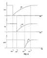
- Waveform 400illustrates the voltage on a sensor element (capacitor) of a row receiving blue light.
- Waveform 402illustrates the voltage on a sensor element of a row receiving red light.
- Waveform 404illustrates the voltage on a sensor element of a row receiving white light.
- t 1(406)
- the blue sensoris discharged.
- the blue sensorreceives the least light intensity and therefore is discharged first.
- time t 2 (408)the red sensor is discharged.
- the white sensoris discharged last at time t 3 (410). All three sensor voltages are then read simultaneously at time t 4 (412) for digitizing.
- Figure 5illustrates the method of the invention.
- the sensor assemblyreceives light from the image (500).
- the filtering step (502)is depicted as a dashed box to illustrate that, preferably, no filter is required but a visual spectrum (white) bandpass filter may be needed if the light source has significant light outside the visual spectrum.
- the light for the unfiltered rowis measured over a finite period of time (504), and digitized into a first numerical value (506).
- the first numerical valueis the sensor system output (510).
Landscapes
- Engineering & Computer Science (AREA)
- Multimedia (AREA)
- Signal Processing (AREA)
- Physics & Mathematics (AREA)
- Spectroscopy & Molecular Physics (AREA)
- Facsimile Heads (AREA)
- Facsimile Scanning Arrangements (AREA)
- Image Input (AREA)
Description
- This invention relates generally to optical image scanners and light sensorassemblies for optical image scanners and more specifically to scanning both grayscale and color images with a color scanner.
- Optical image scanners convert printed pages, photographs, transparentimages and other images from paper or film into a digital form suitable foranalysis and processing by a computer. Both color and gray scale optical imagescanners are available. There is a need for improvement in scanning gray scaleimages with a color scanner, as described below.
- In an optical image scanner, a light source is reflected from a document ortransmitted through a transparent image onto an array of optical sensors, eachsensor measuring the intensity of light received by that sensor. Gray scale scannersmeasure reflected or transmitted light intensity but do not distinguish colors. Indedicated gray scale scanners, a single broad spectrum light source may beprojected onto the sensors, but typically, gray scale scanners use a relativelynarrow spectrum light source having a yellow-green spectrum. In color scanners,light is typically separated into at least three spectral bands, for example red,green and blue bands. In some color scanners, color separation is accomplished bythe use of multiple light sources, each having a different narrow color spectrum.In some color scanners, a single white light source is used and color separation isaccomplished by the use of multiple color filters, each limiting the spectrumreceived by the optical sensors. In this application, a combination of devices to sense a narrow portion of the visual spectral range is called a channel. Forexample, most color scanners have a red channel, a blue channel and a greenchannel, where a channel may be implemented as a narrow spectrum light sourceand sensor or a filter and sensor.
- In some color scanners, a single sensor array is used, and the detection ofthe various color bands is sequential. In sequential scanners having multiplenarrow spectrum light sources, the light sources are sequentially turned on andthen off. In sequential scanners having multiple color filters, the filters aresequentially placed between the light source and the sensors. In other colorscanners, the detection of the various color bands is parallel, typically byemploying multiple sensor arrays to simultaneously receive the various colorbands. For example, beam splitting filters may be used to direct one colorcomponent to one sensor array while directing other color components to othersensor arrays. Alternatively, each sensor array may have an individual filter sothat different color components may be obtained simultaneously, but typicallyfrom different parts of the scanned image. For general background and an exampleof a color image scanner having parallel detection of the various color bands, seeK. Douglas Gennetten and Michael J. Steinle, "Designing a Scanner with ColorVision,"Hewlett-Packard Journal, 44, No. 4 (August, 1993) pp 52-58.
- There are multiple reasons for generating gray scale digitized images usinga color scanner. One primary use of gray scale images is for scanning pages ofblack and white text for optical character recognition. Even for images, theoriginal image may be gray scale only, so that additional memory for color is notneeded. Even if an original image is in color, it may be desirable to digitize theimage as a gray scale image, for example to reduce the memory required to storethe image, to print the image using a printer that only has black and whiteprinting, or to perform image analysis that may not use color information.Typically, the amount of data stop for a digitized color image is three times the data required for a digitized gray scale image (assuming the light is separated intothree bands).
- In addition to memory considerations, scanning a gray scale image as acolor image in a color scanner generally requires more time than scanning the grayscale image using a dedicated gray scale scanner. Therefore, it is also desirable toscan directly in gray scale with a color scanner to improve scanning speed.However, in some color scanner designs, gray scale scanning in a color scanner isinherently slower than gray scale scanning using a dedicated gray scale scanner.There are a number of approaches to generating a gray scale digitized image usinga color scanner. For example, for scanners using multiple narrow spectrum lightsources, all the sources may be turned on simultaneously. For scanners usingfilters, the scanner may use only one color filter (for example, green).Alternatively, for scanners using filters and multiple sensors, signals from all thesensors may be electronically (or arithmetically) combined to obtain arepresentation of the total visible light impinging on the sensors. Filters, however,necessarily reduce the intensity of light that impinges upon the optical sensors.With filtered light, longer exposure times are required to achieve a signal to noiseratio equivalent to that obtained using unfiltered light.
- IBM Technical Disclosure Bulletin, Vol. 20, No. 1, June1977, pages 436 to 437 relates to a silicon solid-state FETcolor scanner. This color scanner is fabricated on a singlesilicon chip with blue, green and red video separateoutputs. The individual photocell unit of the deviceconsists of three continuous photodetectors, each having itscorresponding spectral response, such as blue, red andluminance or white. These photocell units are arranged in aline.
- JP-A-4 053 344 concerns a picture reader, using twofrequency clock signals, a fast clock and a slower clock,for reading out the signal from the CCD.
- US-A-5,105,264 concerns a color image sensor having anoptimum exposure time for each color, wherein the exposurestarts at different times for the respective color sensors.
- Starting from this prior art, it is the object of thepresent application to provide a color image scanner and amethod which has the ability to generate gray scale imagesignals with the speed of a dedicated gray scale scanner.
- This object is achieved by an optical image scanneraccording to
claim 1 and by a method according toclaim 5. - A sensor assembly is provided having three channels. Two of the channelshave color filters. The third channel is receptive to the entire visual color range(white light). For gray scale scanning, only the white channel is used. Using awhite channel for gray scale scanning maximizes the intensity of light impingingon the optical sensors, thereby maximizing scanning speed at any particular signal to noise ratio. In the example embodiment, each color filter is a bandpass filterpassing one of two narrow color bands. For color scanning, three numbersrepresenting digitized intensities from each of the three channels are linearlytransformed into three colors of interest. In the example embodiment, buffering isrequired for color scanning. For color scanning, the charge time per scan line forthe white channel is reduced relative to the charge time for the color channels tomaximize the signal to noise ratio without saturation of the white channel sensors.An optional bandpass filter passing the visual range of wavelengths to the whitechannel provides better accuracy when using a light source that has significantintensity outside the human visual range.
- Figure 1 is a simplified mechanical block diagram illustrating three lines of animage focussed onto three rows of a sensor assembly.
- Figure 2A is a simplified plane front view of a sensor assembly.
- Figure 2B is a simplified side view of the sensor assembly of figure 2A.
- Figure 3 is a block diagram schematic of the sensor assembly in conjunction withmemory and arithmetic units.
- Figure 4 is a timing diagram illustrating variable charge starting times for thedifferent sensor rows when scanning color images.
- Figure 5 is a flow chart illustrating the method of the invention.
- Figure 1 is a simplified mechanical block diagram illustrating a basicscanner configuration. In figure 1, an
image 100 is focussed by alens system 102onto asensor assembly 104. In particular, three separate image scan lines (106,108 and 110) are focussed onto three sensor array rows (112, 114 and 116respectively). In the example embodiment, the sensor assembly comprises threerows of charge coupled devices (CCD's) as the light detection devices. As anexample of scale, for typical commercially available sensor arrays, the width ofthesensor array rows image scan lines image 100 to thesensor assembly 104 is longer than the length of the scanner sothe optical path is folded via multiple mirrors. Thelens assembly 102 is typically acomplex arrangement of multiple lenses. - Figure 2A is a simplified front view of the
sensor assembly 104 depicted infigure 1. As illustrated in figure 2A, the sensor assembly has three rows ofindividual sensor elements. Row 112 is comprised ofindividual sensor elements 200,row 114 is comprised ofindividual sensor elements 202 androw 116 iscomprised ofindividual sensor elements 204. For simplicity of illustration, only 16sensor elements per row are depicted. In commercially available CCD sensorassemblies, the number of sensor elements per row is typically in the range of2,000 - 7,000. Figure 2A also depicts three pairs of signal leads, 210, 212 and214. In the CCD assembly depicted in figure 2A, accumulated charge from eachindividual photosensitive element is transferred to a corresponding capacitor forserial output. Capacitor voltages are serially shifted out the signal leads so that for any one shift cycle, a voltage at a signal lead is a measurement of the lightintensity received earlier by one photosensitive element. - In a typical scanner utilizing three sensor rows as depicted in figure 2A, allthree sensor rows have a filter, either on the surface of the sensors or via externalbeam splitting. Typically, one row is filtered to detect light in a red band ofwavelengths, a second row is filtered to detect light in a green band ofwavelengths, and the third row is filtered to detect light in a blue band ofwavelengths.
- In the invention, two sensor rows are filtered and the third sensor rowreceives unfiltered (white) light (or perhaps filtered to exclude light outside thehuman visual range, as discussed further below). In the invention, for gray scalescanning, only the unfiltered (white) light signal is used. As will be discussedbelow, using the unfiltered light signal enables gray scale scanning to be fasterthan color scanning. For color scanning in the invention, three numbersrepresenting white and two color bands are linearly transformed into three colorintensities.
- Figure 2B is a simplified side view of the
sensor assembly 104 asconfigured in the invention. In figure 2B, two sensor rows (112 and 116) arecovered by color light filters (206 and 208, respectively). One row (114) remainsuncovered. The choice of which one of three color bands is eliminated forsensorrow 114 is arbitrary. Note also that the choice of which sensor row (112, 114,116) is the unfiltered sensor row is arbitrary. Figure 2B illustrates themiddlesensor row 114 as being the unfiltered row but any one of the three sensor rows(112, 114 and 116) can be the unfiltered row. - Red, green and blue color bandpass filters are the most common filtersused in color optical image scanners. Yellow, magenta and cyan bandstop filtersmay also be used. For purposes of example only, the
sensor assembly 104 couldprovide approximate red, white, and blue intensity measurements. With idealfilters, green is white minus the sum of red and blue. In general, however, the filters are not ideal and a general linear transformation is required. In general,almost any three filters can be used as long as they pass or stop three non-identicalbands of visible wavelengths, provided that these bands permit acceptable colorreproduction using known principles of color science. Given three numbersrepresenting the intensity of three bands, other colors can be obtained bymultiplying the three measured values by a 3x3 transformation matrix. Using theexample colors again, red, white, and blue may be linearly transformed into red,green and blue for display purposes. For printing purposes, red, white, and bluemay be transformed into yellow, magenta, and cyan. - One additional potential problem may require an additional refinement ofthe color filters illustrated in figure 2B. In the typical arrangement where all threesensor rows have filters and where the filters are bandpass filters, lightwavelengths outside the human visual range (wavelengths in the range from 400 to700 nanometers) are inherently excluded by the bandpass filters. If
sensor row 114has no filter, light outside the human visual range but within the range ofphotosensitivity of the sensors may distort the intensity measured by the sensors. Ifthe light source used by the scanner has significant intensity outside the humanvisual range, thensensor row 114 may need a white bandpass filter passing therange from 400 to 700 nanometers. Finally, it may also be desirable that this whitefilter also suppress some visible wavelengths to improve color reproduction perknown principles of color science. For example, rather than a strictly white filter,a broadband dominantly green filter that also passes substantial amounts of red andblue light might be employed. In general, the white filter must be significantlybroader in bandwidth than a typical color filter in order to achieve faster grayscale scans. - Referring back to figure 1, in order to scan the
entire image 100, theimage 100 must move relative to thesensor assembly 104. It does not matter whether theimage 100 moves past astationary sensor assembly 104 or whether thesensorassembly 104 moves past astationary image 100. Note that for an optical arrangement as illustrated, three different scan lines (106, 108, and 110) onimage 100 are being focussed onsensor assembly 104. Assume for discussion that thedirection of relative movement is as illustrated byarrow 118 in figure 1. Withrelative movement as indicated byarrow 118,image scan line 106 depicted ascurrently focussed onto thesensor row 112 was earlier focussed onto thesensorrow 114 and earlier still was focussed ontosensor row 116. The color of aparticular picture element fromimage scan line 106 is obtained by linearlytransforming the color measurement atsensor row 112 along with colormeasurements obtained earlier fromsensor rows sensor rows - Figure 3 illustrates the memory buffers and arithmetic elements requiredfor color scanning. In figure 3, analog voltages from the CCD rows are convertedinto numerical values by analog to digital (A/D)
converters 300. Numerical valuesfrom all the CCD's insensor row 116 are sequentially stored into memory buffer306. To facilitate discussion, memory buffer 306 is depicted as being configuredinto an array of rows and columns, but can be alternatively configured in aserpentine serial fashion, as a first-in-first-out (FIFO) stack buffer, or effectivelyconfigured into rows and columns using random access memory. When the image100 (figure 1) moves relative to thesensor assembly 104 so thatsensor row 116 isfocussed onto a new scan line, the stored row of numbers in the memory buffer306 is effectively shifted (upward in figure 3) from row i (320) to row i+1 (322).When the image 100 (figure 1) has moved a distance relative to thesensorassembly 104 corresponding to the distance betweenimage scan lines 106 and 110(figure 1), then the top row i+8 (324) of memory buffer 306 contains numericalvalues from an earlier scan ofscan line 106, at the same time thatsensor row 112is receiving light fromscan line 106. - In figure 3, the memory buffer 306 is depicted as corresponding to aspacing of 8 image scan lines between
image scan lines image scan lines sensor row 114 must be buffered in a memory buffer304. Finally, in figure 3, numerical information fromsensor row 112 needs onlya single row ofmemory 302, if any. - Also illustrated in figure 3 are the arithmetic elements required to obtainthree colors in a color scan. For one picture element at a time, a
buffered number 312 fromsensor row 116, a correspondingnumber 310 fromsensor row 114, andacorresponding number 308 fromsensor row 112 form a3x1 matrix 314.Matrix 314 is multiplied by apredetermined 3x3 matrix 316 to generate a triplet ofnumerical values 318.Numerical values 318 may be used directly for display orprinting as appropriate. - Light impinging on the photosensitive portion of a CCD results in chargethat accumulates on a capacitor, resulting in a voltage on the capacitor. Typically,the capacitor is initially discharged and then is allowed to charge as it is exposedto light. The longer the exposure, the better the signal to noise ratio. There is,however, a finite voltage limit (saturation).
- In the arrangement illustrated in figure 2B, the intensity of the unfilteredlight impinging on
sensor row 114 is generally greater than the intensity of lightpassing through the filters onrows sensorrow 114 is three times the intensity of light passing through the filters onrows rows unfiltered sensor row 114 might saturate. Therefore, to maximize the signal to noise ratio without saturating the unfiltered sensors, theunfiltered sensor row 114 needs to beexposed for a shorter amount of time than the two filteredsensor rows filters rows unfiltered sensor row 114 chargetime should be one third the charge time of the two filteredsensor rows - Figure 4 illustrates the relative timing for discharge and reading of threesensor rows when scanning color images.
Waveform 400 illustrates the voltage ona sensor element (capacitor) of a row receiving blue light.Waveform 402illustrates the voltage on a sensor element of a row receiving red light.Waveform 404 illustrates the voltage on a sensor element of a row receiving white light. Attime t1 (406), the blue sensor is discharged. The blue sensor receives the least lightintensity and therefore is discharged first. At time t2 (408), the red sensor isdischarged. The white sensor is discharged last at time t3 (410). All three sensorvoltages are then read simultaneously at time t4 (412) for digitizing. - When scanning a gray scale image, the above discussion of buffering andcharge time adjustment between sensor rows is irrelevant. When scanning a grayscale image, only the
unfiltered sensor row 114 is used and the charge times arereduced to the minimum required to maximize the signal to noise ratio for theunfiltered sensor row 114. For example, in figure 4, for gray scale scanning, the time from t1 (406) to t3 (410) can be eliminated. In addition, no buffering ofnumerical data is needed. Therefore, gray scale scanning can be made substantiallyfaster than color scanning. - Figure 5 illustrates the method of the invention. The sensor assemblyreceives light from the image (500). For one row, the filtering step (502) isdepicted as a dashed box to illustrate that, preferably, no filter is required but avisual spectrum (white) bandpass filter may be needed if the light source hassignificant light outside the visual spectrum. The light for the unfiltered row ismeasured over a finite period of time (504), and digitized into a first numericalvalue (506). For gray scale scanning, the first numerical value is the sensor systemoutput (510).
- For color scanning, for the two color filtered rows, light passes throughcolor filters (512, 514), is measured over a period of time (516, 518) and isdigitized into second and third digital values. Digitized values from at least tworows are buffered (524, 526 and 528) (recall that one buffer may not be necessaryas depicted by box 528). Then, a linear transformation is computed (530) (as infigure 3, 314, 316 and 318), generating three transformed numbers (532). Asillustrated in figure 5, fewer steps are needed for gray scale scanning.
Claims (6)
- An optical image scanner for generating gray scale orcolor image signals comprising:a sensor assembly (104) comprisinga row (114) of first sensor elements (202), each firstsensor element receiving light that is unfiltered andhaving an analog output signal proportional to the receivedlight, the first row of first sensor elements having a first charge time; anda plurality of rows (112,116) of second sensor elements(200,204), each second sensor element receiving light thatis filtered and having an analog output signal proportionalto the received light, each row of second sensor elements having second charge times,said sensor assembly (104) being controllable to be run ina first mode of operation or in a second mode of operation,wherein in said first mode of operation said optical imagescanner derives said gray scale image signals only from theoutput of said first sensor elements (202), said first mode ofoperation having one charge time for the rows of first and second sensor elements reduced to said first charge time; andwherein in said second mode of operation said optical imagescanner derives said color image signals from the output ofboth said first and said second sensor elements (202,200,204),said second mode of operation having both of said first and second charge times, saidfirst charge time being less than said second charge times.
- The optical image scanner of claim 1 wherein the row offirst sensor elements (202) is modified in that each firstsensor element receives light that is filtered by a bandpasslight filter passing substantially all the human visible lightspectrum, said human visible light spectrum ranging form 400 to700 nanometers;in a first row of said plurality of second sensor elements,each second sensor element receives light that is filtered by ablue bandpass filter (206); andin a second row of said plurality of second sensorelements, each second sensor element receives light that isfiltered by a red bandpass filter (206).
- The optical image scanner of claim 2 wherein each of thefirst sensor elements has an analog output signal;a first analog-to-digital converter is provided, receivingone of the analog output signals from the first sensor elementsand outputting a first numerical value representing anamplitude of the received analog signal;each of the second sensor elements has an analog outputsignal;a plurality of second analog-to-digital converters areprovided, each corresponding to one row of the plurality ofrows of second sensor elements, each receiving one analogoutput signal from its corresponding row of second sensorelements and outputting a second numerical value representingan amplitude of the received analog signal; andan arithmetic unit is provided, receiving the firstnumerical value and the second numerical values and performinga linear transformation on the received values.
- The optical image scanner as in claim 3 comprising:a first memory buffer (302), receiving the first numericalvalue and outputting the received numerical value on a first-infirst-out basis to the arithmetic unit; anda plurality of second memory buffers (304,306), one secondmemory buffer for each row of the plurality of rows of secondsensor elements, each second memory buffer receiving the secondnumerical values from its corresponding row of second sensorelements and outputting the received second numerical values ona first-in first-out basis to the arithmetic unit.
- A method of measuring light intensity within aparticular spectral band in a color optical image scanner,comprising the following steps:(a) exposing a first sensor element to unfiltered light, the first sensor element havinga first charge time;(b) digitizing (506) an analog output from the first sensorelement into a first numerical value;(c) filtering (512) the light through a first bandpass light filter for a second sensor element, the second sensor element having a second chargetime, said first charge time being less than said second chargetime;(d) filtering (514) the light through a second bandpasslight filter for a third sensor element, the third sensor element having a third chargetime, said first and second charge times being less than saidthird charge time;(e) digitizing (520,522) an analog output from the secondand third sensor elements into second and third numericalvalues respectively;(f) computing (530) the light intensity within theparticular spectral band as a linear transformation of thefirst, second and third numerical values;(g) scanning (510) a gray scale image by reducing the second and third charge times to the first charge time and by repeating steps(a) and (b); or(h) scanning (532) a color image by repeating steps (a)through (f).
- The method of claim 5, further comprising the followingmodifications:step (a) modified by filtering (502) the light through awhite light filter, the white light filter passingsubstantially all the human visible light spectrum, said humanvisible light spectrum ranging form 400 to 700 nanometers;the first bandpass filter of step (b) is a blue bandpassfilter; andthe second bandpass filter of step (c) is a red band passfilter.
Applications Claiming Priority (2)
| Application Number | Priority Date | Filing Date | Title |
|---|---|---|---|
| US29470094A | 1994-08-23 | 1994-08-23 | |
| US294700 | 1994-08-23 |
Publications (2)
| Publication Number | Publication Date |
|---|---|
| EP0698994A1 EP0698994A1 (en) | 1996-02-28 |
| EP0698994B1true EP0698994B1 (en) | 2000-02-02 |
Family
ID=23134550
Family Applications (1)
| Application Number | Title | Priority Date | Filing Date |
|---|---|---|---|
| EP95111084AExpired - LifetimeEP0698994B1 (en) | 1994-08-23 | 1995-07-14 | Sensor assembly providing gray scale and color for an optical image scanner |
Country Status (4)
| Country | Link |
|---|---|
| US (1) | US5773814A (en) |
| EP (1) | EP0698994B1 (en) |
| JP (1) | JPH0879443A (en) |
| DE (1) | DE69514874T2 (en) |
Families Citing this family (41)
| Publication number | Priority date | Publication date | Assignee | Title |
|---|---|---|---|---|
| US6005680A (en)* | 1995-04-04 | 1999-12-21 | Canon Information Systems, Inc. | Method for capturing a document image, a scanner using the method and a document image management system using the scanner |
| US5892595A (en)* | 1996-01-26 | 1999-04-06 | Ricoh Company, Ltd. | Image reading apparatus for correct positioning of color component values of each picture element |
| US5898509A (en)* | 1996-10-15 | 1999-04-27 | Hewlett-Packard Company | Method for improving the signal-to-noise ratio of a CCD sensor in a color imaging device |
| US5920407A (en)* | 1997-01-09 | 1999-07-06 | Hewlett-Packard Company | Method and apparatus for applying tonal correction to image data |
| US6407830B1 (en)* | 1999-02-05 | 2002-06-18 | Hewlett-Packard Co. | Sensor assemblies for color optical image scanners optical scanner and methods of scanning color images |
| US6356672B1 (en) | 1999-03-08 | 2002-03-12 | Sharp Laboratories Of America, Inc. | Method and apparatus for reducing the color registration artifact of image capture devices |
| TW475330B (en)* | 1999-10-29 | 2002-02-01 | Hewlett Packard Co | Photosensor array with multiple different sensor areas |
| US6532086B1 (en)* | 1999-11-19 | 2003-03-11 | Xerox Corporation | Optical color matrixing using time delay and integration sensor arrays |
| US6650438B1 (en) | 1999-12-01 | 2003-11-18 | Sharp Laboratories Of America, Inc, | Construction of a color transform to reduce effects of scanner metamerism |
| JP4139051B2 (en)* | 2000-06-28 | 2008-08-27 | 富士フイルム株式会社 | Linear image sensor chip and linear image sensor |
| US6465801B1 (en) | 2000-07-31 | 2002-10-15 | Hewlett-Packard Company | Dust and scratch detection for an image scanner |
| JP2002084397A (en)* | 2000-09-11 | 2002-03-22 | Fuji Xerox Co Ltd | Image reader |
| US6765703B1 (en)* | 2000-09-27 | 2004-07-20 | Kabushiki Kaisha Toshiba | Method and apparatus for sensing image |
| US6831761B2 (en)* | 2001-03-30 | 2004-12-14 | Eastman Kodak Company | Document scanner having a selectable range of resolutions with reduced processing |
| US6941025B2 (en)* | 2001-04-19 | 2005-09-06 | International Business Machines Corporation | Simultaneous vertical spatial filtering and chroma conversion in video images |
| US6961157B2 (en)* | 2001-05-29 | 2005-11-01 | Xerox Corporation | Imaging apparatus having multiple linear photosensor arrays with different spatial resolutions |
| US7323676B2 (en)* | 2001-09-11 | 2008-01-29 | Lumileds Lighting Us, Llc. | Color photosensor with color filters and subtraction unit |
| US7034957B2 (en)* | 2002-04-15 | 2006-04-25 | Shang-Yu Yang | Method for increasing signal to noise ratio |
| US7274496B2 (en)* | 2003-03-04 | 2007-09-25 | Kabushiki Kaisha Toshiba | 4-line CCD sensor and image input apparatus using the same |
| US7301681B2 (en)* | 2003-03-06 | 2007-11-27 | Kabushiki Kaisha Toshiba | System and method for processing documents with four-line CCD sensor |
| US7057155B2 (en)* | 2004-07-29 | 2006-06-06 | Boon Keat Tan | Color sensor system with voltage offset correction |
| US7611060B2 (en) | 2005-03-11 | 2009-11-03 | Hand Held Products, Inc. | System and method to automatically focus an image reader |
| EP3920079B1 (en)* | 2005-03-11 | 2023-06-28 | Hand Held Products, Inc. | Digital picture taking optical reader having hybrid monochrome and color image sensor array |
| US7780089B2 (en) | 2005-06-03 | 2010-08-24 | Hand Held Products, Inc. | Digital picture taking optical reader having hybrid monochrome and color image sensor array |
| US7568628B2 (en) | 2005-03-11 | 2009-08-04 | Hand Held Products, Inc. | Bar code reading device with global electronic shutter control |
| US20060238830A1 (en)* | 2005-04-21 | 2006-10-26 | Peter Dikeman | Color image capture system |
| US7770799B2 (en) | 2005-06-03 | 2010-08-10 | Hand Held Products, Inc. | Optical reader having reduced specular reflection read failures |
| US8139130B2 (en) | 2005-07-28 | 2012-03-20 | Omnivision Technologies, Inc. | Image sensor with improved light sensitivity |
| US8274715B2 (en) | 2005-07-28 | 2012-09-25 | Omnivision Technologies, Inc. | Processing color and panchromatic pixels |
| US20070046807A1 (en)* | 2005-08-23 | 2007-03-01 | Eastman Kodak Company | Capturing images under varying lighting conditions |
| TW200709662A (en)* | 2005-08-24 | 2007-03-01 | Lite On Technology Corp | Contact image sensor |
| JP4487944B2 (en)* | 2006-02-09 | 2010-06-23 | ソニー株式会社 | Solid-state imaging device |
| US7916362B2 (en) | 2006-05-22 | 2011-03-29 | Eastman Kodak Company | Image sensor with improved light sensitivity |
| US8031258B2 (en) | 2006-10-04 | 2011-10-04 | Omnivision Technologies, Inc. | Providing multiple video signals from single sensor |
| US20080174839A1 (en)* | 2007-01-24 | 2008-07-24 | Kevin Youngers | Full color optical image scanning |
| GB2456492B (en)* | 2007-07-05 | 2012-09-26 | Hewlett Packard Development Co | Image processing method, image capture device, and computer readable medium |
| US7855740B2 (en)* | 2007-07-20 | 2010-12-21 | Eastman Kodak Company | Multiple component readout of image sensor |
| GB2457306B (en)* | 2008-02-11 | 2013-02-27 | Thales Holdings Uk Plc | An imaging apparatus |
| US8218068B2 (en) | 2009-04-01 | 2012-07-10 | Omnivision Technologies, Inc. | Exposing pixel groups in producing digital images |
| GB0912981D0 (en)* | 2009-07-27 | 2009-09-02 | St Microelectronics Res & Dev | Imaging system and method |
| JP7118748B2 (en)* | 2018-06-01 | 2022-08-16 | 富士通コンポーネント株式会社 | Meters and optical readers |
Citations (4)
| Publication number | Priority date | Publication date | Assignee | Title |
|---|---|---|---|---|
| JPS60123158A (en)* | 1983-12-07 | 1985-07-01 | Sharp Corp | Image reading device |
| JPH03178262A (en)* | 1989-12-06 | 1991-08-02 | Mitsubishi Electric Corp | Charge transfer method in charge transfer device |
| JPH0453344A (en)* | 1990-06-21 | 1992-02-20 | Ricoh Co Ltd | Picture reader |
| US5105264A (en)* | 1990-09-28 | 1992-04-14 | Eastman Kodak Company | Color image sensor having an optimum exposure time for each color |
Family Cites Families (12)
| Publication number | Priority date | Publication date | Assignee | Title |
|---|---|---|---|---|
| US4087836A (en)* | 1977-01-07 | 1978-05-02 | Bell & Howell Company | Signal processing for an imaging device |
| JPS57102281U (en)* | 1980-12-16 | 1982-06-23 | ||
| JPH0614750B2 (en)* | 1982-12-15 | 1994-02-23 | 池上通信機株式会社 | Color original imaging device |
| EP0119862B1 (en)* | 1983-03-17 | 1990-12-27 | Nec Corporation | Solid-state color imaging apparatus |
| JPS59198754A (en)* | 1983-04-26 | 1984-11-10 | Toshiba Corp | Color solid-state imaging device |
| JPS6320953A (en)* | 1986-07-15 | 1988-01-28 | Toshiba Corp | Image pickup device |
| US5191409A (en)* | 1988-03-29 | 1993-03-02 | Mitsubishi Denki Kabushiki Kaisha | Color scanning system |
| US4992860A (en)* | 1988-03-29 | 1991-02-12 | Mitsubishi Denki Kabushiki Kaisha | Color scanning system |
| JPH01265774A (en)* | 1988-04-18 | 1989-10-23 | Tokyo Electric Co Ltd | image reading device |
| JP3176101B2 (en)* | 1991-11-12 | 2001-06-11 | キヤノン株式会社 | Image reading device |
| US5229595A (en)* | 1991-12-19 | 1993-07-20 | Xerox Corporation | Fluid-filled color filtered input scanner arrays |
| US5336878A (en)* | 1993-05-10 | 1994-08-09 | Hewlett-Packard Company | Variable speed single pass color optical scanner |
- 1995
- 1995-07-14DEDE69514874Tpatent/DE69514874T2/ennot_activeExpired - Fee Related
- 1995-07-14EPEP95111084Apatent/EP0698994B1/ennot_activeExpired - Lifetime
- 1995-08-23JPJP7237769Apatent/JPH0879443A/enactivePending
- 1995-09-22USUS08/532,378patent/US5773814A/ennot_activeExpired - Lifetime
Patent Citations (4)
| Publication number | Priority date | Publication date | Assignee | Title |
|---|---|---|---|---|
| JPS60123158A (en)* | 1983-12-07 | 1985-07-01 | Sharp Corp | Image reading device |
| JPH03178262A (en)* | 1989-12-06 | 1991-08-02 | Mitsubishi Electric Corp | Charge transfer method in charge transfer device |
| JPH0453344A (en)* | 1990-06-21 | 1992-02-20 | Ricoh Co Ltd | Picture reader |
| US5105264A (en)* | 1990-09-28 | 1992-04-14 | Eastman Kodak Company | Color image sensor having an optimum exposure time for each color |
Non-Patent Citations (1)
| Title |
|---|
| M. HERMANN AND J. WÖLBER: "The P CCD 500B linear imager", ELECTRONIC COMPONENTS AND APPLICATIONS, vol. 1, no. 3, pages 183 - 191* |
Also Published As
| Publication number | Publication date |
|---|---|
| US5773814A (en) | 1998-06-30 |
| JPH0879443A (en) | 1996-03-22 |
| EP0698994A1 (en) | 1996-02-28 |
| DE69514874T2 (en) | 2000-07-20 |
| DE69514874D1 (en) | 2000-03-09 |
Similar Documents
| Publication | Publication Date | Title |
|---|---|---|
| EP0698994B1 (en) | Sensor assembly providing gray scale and color for an optical image scanner | |
| US6172352B1 (en) | Sensing module for accelerating signal readout from image sensors | |
| EP1096785B1 (en) | Method of scanning using a photosensor with multiple sensor areas of different sizes | |
| US4891690A (en) | Color image reading apparatus with plural linear sensors which can read different lines of the image | |
| US5753906A (en) | Color separation using multiple point narrow band illumination from N-colors of light sources | |
| US5750985A (en) | High speed and high precisioin image scanning apparatus | |
| US6407830B1 (en) | Sensor assemblies for color optical image scanners optical scanner and methods of scanning color images | |
| US5898509A (en) | Method for improving the signal-to-noise ratio of a CCD sensor in a color imaging device | |
| EP0043721A2 (en) | Device for scanning coloured originals | |
| US7154545B2 (en) | Image scanner photosensor assembly with improved spectral accuracy and increased bit-depth | |
| EP0273638A2 (en) | Image scanner systems | |
| EP0967789A2 (en) | Color image capturing device and image reader using the color image capturing device | |
| US6646682B1 (en) | Linear tri-color image sensors | |
| JPH10200712A (en) | Sweep speed variable-type picture scanner and scanning method | |
| JPH11313194A (en) | Registration device and method for imaging in variable resolution | |
| US6765699B1 (en) | Photosensor array with decreased scan time for decreased optical sampling rates | |
| JP3839942B2 (en) | Multiple image generation method | |
| US7605958B2 (en) | Design parameters for a multi-row linear photosensor array | |
| US20020001031A1 (en) | Color image pickup element, image reader using the pickup element, and image reading method | |
| EP1009159A2 (en) | Multiple photo sensor row scanning apparatus | |
| JPH08251347A (en) | Synchronous addition type color linear image sensor | |
| JPH114326A (en) | Image pickup device | |
| JPH0730729A (en) | Image input device | |
| JP2908136B2 (en) | Optical spectrometer for solid-state imaging device | |
| JP3818790B2 (en) | Color image reader |
Legal Events
| Date | Code | Title | Description |
|---|---|---|---|
| PUAI | Public reference made under article 153(3) epc to a published international application that has entered the european phase | Free format text:ORIGINAL CODE: 0009012 | |
| AK | Designated contracting states | Kind code of ref document:A1 Designated state(s):DE FR GB | |
| 17P | Request for examination filed | Effective date:19960816 | |
| 17Q | First examination report despatched | Effective date:19960923 | |
| GRAG | Despatch of communication of intention to grant | Free format text:ORIGINAL CODE: EPIDOS AGRA | |
| GRAG | Despatch of communication of intention to grant | Free format text:ORIGINAL CODE: EPIDOS AGRA | |
| GRAG | Despatch of communication of intention to grant | Free format text:ORIGINAL CODE: EPIDOS AGRA | |
| GRAH | Despatch of communication of intention to grant a patent | Free format text:ORIGINAL CODE: EPIDOS IGRA | |
| GRAH | Despatch of communication of intention to grant a patent | Free format text:ORIGINAL CODE: EPIDOS IGRA | |
| GRAA | (expected) grant | Free format text:ORIGINAL CODE: 0009210 | |
| AK | Designated contracting states | Kind code of ref document:B1 Designated state(s):DE FR GB | |
| REF | Corresponds to: | Ref document number:69514874 Country of ref document:DE Date of ref document:20000309 | |
| ET | Fr: translation filed | ||
| PLBE | No opposition filed within time limit | Free format text:ORIGINAL CODE: 0009261 | |
| STAA | Information on the status of an ep patent application or granted ep patent | Free format text:STATUS: NO OPPOSITION FILED WITHIN TIME LIMIT | |
| 26N | No opposition filed | ||
| RAP2 | Party data changed (patent owner data changed or rights of a patent transferred) | Owner name:HEWLETT-PACKARD COMPANY, A DELAWARE CORPORATION | |
| REG | Reference to a national code | Ref country code:GB Ref legal event code:732E | |
| REG | Reference to a national code | Ref country code:GB Ref legal event code:IF02 | |
| REG | Reference to a national code | Ref country code:FR Ref legal event code:TP | |
| PGFP | Annual fee paid to national office [announced via postgrant information from national office to epo] | Ref country code:DE Payment date:20070831 Year of fee payment:13 | |
| PGFP | Annual fee paid to national office [announced via postgrant information from national office to epo] | Ref country code:GB Payment date:20070727 Year of fee payment:13 | |
| PGFP | Annual fee paid to national office [announced via postgrant information from national office to epo] | Ref country code:FR Payment date:20070717 Year of fee payment:13 | |
| GBPC | Gb: european patent ceased through non-payment of renewal fee | Effective date:20080714 | |
| PG25 | Lapsed in a contracting state [announced via postgrant information from national office to epo] | Ref country code:DE Free format text:LAPSE BECAUSE OF NON-PAYMENT OF DUE FEES Effective date:20090203 | |
| REG | Reference to a national code | Ref country code:FR Ref legal event code:ST Effective date:20090331 | |
| PG25 | Lapsed in a contracting state [announced via postgrant information from national office to epo] | Ref country code:GB Free format text:LAPSE BECAUSE OF NON-PAYMENT OF DUE FEES Effective date:20080714 | |
| PG25 | Lapsed in a contracting state [announced via postgrant information from national office to epo] | Ref country code:FR Free format text:LAPSE BECAUSE OF NON-PAYMENT OF DUE FEES Effective date:20080731 |