EP0692894B1 - Optimum signal decision apparatus for digital signal receiver - Google Patents
Optimum signal decision apparatus for digital signal receiverDownload PDFInfo
- Publication number
- EP0692894B1 EP0692894B1EP95111068AEP95111068AEP0692894B1EP 0692894 B1EP0692894 B1EP 0692894B1EP 95111068 AEP95111068 AEP 95111068AEP 95111068 AEP95111068 AEP 95111068AEP 0692894 B1EP0692894 B1EP 0692894B1
- Authority
- EP
- European Patent Office
- Prior art keywords
- signal
- received
- component
- level
- strength
- Prior art date
- Legal status (The legal status is an assumption and is not a legal conclusion. Google has not performed a legal analysis and makes no representation as to the accuracy of the status listed.)
- Expired - Lifetime
Links
- 229920006395saturated elastomerPolymers0.000claimsdescription20
- 238000010276constructionMethods0.000description6
- 238000010586diagramMethods0.000description6
- 238000000034methodMethods0.000description6
- 230000005684electric fieldEffects0.000description4
- 239000000284extractSubstances0.000description3
- 230000002238attenuated effectEffects0.000description2
- 238000001514detection methodMethods0.000description2
- 238000010295mobile communicationMethods0.000description2
- 238000006243chemical reactionMethods0.000description1
- 239000012050conventional carrierSubstances0.000description1
- 238000007796conventional methodMethods0.000description1
- 238000012986modificationMethods0.000description1
- 230000004048modificationEffects0.000description1
- 238000001228spectrumMethods0.000description1
Images

Classifications
- H—ELECTRICITY
- H04—ELECTRIC COMMUNICATION TECHNIQUE
- H04L—TRANSMISSION OF DIGITAL INFORMATION, e.g. TELEGRAPHIC COMMUNICATION
- H04L27/00—Modulated-carrier systems
- H04L27/18—Phase-modulated carrier systems, i.e. using phase-shift keying
- H04L27/22—Demodulator circuits; Receiver circuits
- H—ELECTRICITY
- H04—ELECTRIC COMMUNICATION TECHNIQUE
- H04L—TRANSMISSION OF DIGITAL INFORMATION, e.g. TELEGRAPHIC COMMUNICATION
- H04L25/00—Baseband systems
- H04L25/02—Details ; arrangements for supplying electrical power along data transmission lines
- H04L25/06—DC level restoring means; Bias distortion correction ; Decision circuits providing symbol by symbol detection
- H04L25/061—DC level restoring means; Bias distortion correction ; Decision circuits providing symbol by symbol detection providing hard decisions only; arrangements for tracking or suppressing unwanted low frequency components, e.g. removal of DC offset
- H04L25/062—Setting decision thresholds using feedforward techniques only
Definitions
- This inventionrelates to a digital modulated signal receiver, and more particularly to a carrier detector for a linear digital modulated signal receiver.
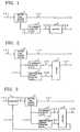
- Fig. 1is a block diagram showing the construction of a conventional carrier detector.
- Received signal 101is inputted to received signal strength detector 2, from which received signal 103 and received strength signal 104 are outputted.
- a logarithmic amplifier or the likeis used for received signal strength detector 2.
- Received strength signal 104is produced by signal conversion based on a control signal (for example, a gain control signal) in the logarithmic amplifier for securing a logarithmic linearity of the amplifier and is generally called RSSI (Received Signal Strength Indicator).
- RSSIReceived Signal Strength Indicator
- DC component extracting filter 3receives received strength signal 104 and extracts DC component 105 of received strength signal 104.
- Decision circuit 8compares a voltage value corresponding to DC component 105 with a predetermined level and outputs decision signal 108 which represents whether or not the strength of the received signal is sufficiently high.
- the received signalmay possibly be selected as it is, resulting in error in selection of an optimum received signal.
- a countermeasure to this problemis disclosed, for example, in JP-A-04343547 wherein, when the field strength of a received signal is higher than a certain level, the output of the received signal is attenuated by an attenuator to a level with which the receiver is not saturated.
- a four-phase phase modulation signal inputted to a high frequency receiving partis converted into an intermediate frequency signal and the converted signal is outputted and demodulated by the demodulation part and outputted.
- Baud timing for extracting a digital signal from the demodulation partis applied from an amplitude information detecting part for detecting an amplitude variation component from the intermediate frequency signal and extracting timing.
- an electric field information detecting partmonitors the intensity of an electric field based upon the intermediate frequency signal in each baud timing. At the time of inputting the four-phase phase modulation signal with a strong electric field, the intermediate frequency signal is saturated, but the detecting part detects the storing electric field state and reduces the gain of the receiving part, preventing the intermediate frequency signal from being saturated.
- the amplitude variation componentcan be always effectively detected.
- the result of detection of the received signal strengthis required to have a monotonous increasing characteristic with respect to the received signal level.
- the monotonous increasing characteristicis lost if the receiver is saturated, it is indefinite whether the RSSI output level with respect to the input level of the received signal exhibits a condition wherein the output of the received signal is fully saturated with respect to a certain RSSI output level or another condition wherein the output of the received signal is not saturated as yet.
- the prior art methodhas a problem in that, since it cannot be decided whether the RSSI output level is nearly in a saturated condition or is in a saturated condition, it cannot be determined how the attenuator should be controlled. Consequently, with the prior art method, an optimum received signal is not necessarily selected.
- a received signal decision apparatusfor a digital modulated signal receiver, comprising received signal strength detecting means for detecting a received signal strength corresponding to an envelope of a received signal and outputting a received strength signal, a DC component extracting filter for extracting a DC component of the received strength signal, a modulation rate component extracting filter for extracting a modulation rate component of the received strength signal, and decision means for deciding based on the DC component and the modulation rate component of the received strength signal whether or not the received signal is optimum.
- the decision of the decision meansmay be based on the relationship between the DC component and the modulation rate component of the received signal described above, and it may decide that the received signal is optimum
- the decision meansmay calculate a ratio of the DC component to the modulation rate component of the received strength signal or a reciprocal ratio to this ratio for each of the candidates and decide that that one of the alternatives for the signal to be received whose ratio exhibits the highest value or whose reciprocal rate exhibits the lowest value is optimum as the received signal.
- a received signal decision apparatusfor a digital modulated signal receiver, comprising received signal strength detecting means for detecting a received signal strength corresponding to an envelope of a received signal and outputting a received strength signal, a DC component extracting filter for extracting a DC component of the received strength signal, a modulation rate component extracting filter for extracting a modulation rate component of the received strength signal, an attenuator provided on the input side of the received signal strength detecting means, and control means for controlling the attenuator in response to the DC component and the modulation rate component of the received strength signal, the control means continuously controlling the output of the attenuator in accordance with the value of a ratio of the DC component to the modulation rate component of the received strength signal so as to prevent saturation of the output of the receiver, the control means deciding based on the output of the receiver as a result of the control of the attenuator whether or not the received signal is optimum.
- Fig. 2is a block diagram showing an embodiment of a received signal decision apparatus for a digital modulated signal receiver of the present invention.
- received signal strength detector 2produces received strength signal 104 and received signal 103 from received signal 101 inputted thereto.
- Received strength signal 104is outputted as an RSSI detected in accordance with an envelope of received signal 101 as described above to DC component extracting filter 3 and modulation rate component extracting filter 4.
- DC component extracting filter 3is constituted using a low-pass filter (LPF), extracts a DC component of received strength signal 104 and outputs extracted DC component signal 105 having an output level (voltage value or current value) corresponding to the extracted DC component to decision circuit 5.
- LPFlow-pass filter
- modulation rate component extracting filter 4is constituted by a band-pass filter (BPF) and a detector, extracts a line spectrum component corresponding to a modulation rate from received strength signal 104 by means of the band-pass filter and outputs extracted modulation rate component signal 106 having an output level (voltage value or current value) corresponding to the modulation rate component to decision circuit 5.
- BPFband-pass filter
- Decision circuit 5compares the output level of extracted DC component signal 105 with a predetermined threshold level, and when the output level of extracted DC component signal 105 is higher than the threshold level and besides a comparison of the output level of extracted modulation rate component signal 106 with another predetermined threshold level reveals that also-the output level of extracted modulation rate component signal 106 is higher than the threshold level, the decision circuit 5 decides that received signal 101 is an optimum received signal and outputs decision signal 108 representing a result of the decision.
- decision circuit 5may be based either on the method described above wherein the output levels of extracted component signals 105 and 106 are individually compared with respective suitable levels (threshold levels) or on another method wherein a received signal is selected based on the relationship between a modulation rate component and a DC component such that the received signal is decided to be optimum when
- Received signal 101is inputted to received signal strength detector 2 by way of attenuator 1. Further, decision circuit 6 outputs decision signal 108 and further outputs control signal 107 for controlling attenuator 1 in accordance with a result of decision of decision circuit 6 to attenuator 1.
- decision circuit 6selects a received signal in the following manner.
- decision circuit 6decides that the received signal is not optimum, and outputs control signal 107 to increase the attenuation amount of attenuator 1 to lower the gain of the receiver thereby to eliminate an otherwise possible saturated condition of the output of the receiver. Using this result, decision of whether or not the received signal is optimum is performed similarly as in the first embodiment described above. Further in another instance, decision circuit 6 decides that the received signal is not optimum when
- controller 7is employed as shown in Fig. 4.
- the controllercontrols the attenuator so that, for example, the attenuation amount of the attenuator has such a continuous variation that it increases in proportion to or in reciprocal proportion to the ratio of the DC component to the modulation rate component, and based on a result of the control, it is decided by controller 7 whether or not the received signal is optimum.
- a received signal which has a sufficiently high signal strength but is difficult to demodulate due to a difference in modulation rate or due to cochannel interferencecan be selected. Further, according to the present invention, even if the receiver is in a saturated condition and cannot perform demodulation, the received signal can be attenuated without the necessity for a monotonous increasing characteristic of the received signal strength detection result with respect to the received signal level.
Landscapes
- Engineering & Computer Science (AREA)
- Computer Networks & Wireless Communication (AREA)
- Signal Processing (AREA)
- Power Engineering (AREA)
- Digital Transmission Methods That Use Modulated Carrier Waves (AREA)
- Circuits Of Receivers In General (AREA)
- Noise Elimination (AREA)
- Control Of Amplification And Gain Control (AREA)
Description
- This invention relates to a digital modulatedsignal receiver, and more particularly to a carrierdetector for a linear digital modulated signal receiver.
- It is important to measure the signal strength ofa received signal to detect a carrier particularly whensignals from a plurality of base stations are receivedand it is required to select an optimum signal fromamong the received signals as with a terminal stationin mobile communications. Fig. 1 is a block diagramshowing the construction of a conventional carrierdetector. Received
signal 101 is inputted to receivedsignal strength detector 2, from which receivedsignal 103 and received strength signal 104 are outputted. Alogarithmic amplifier or the like is used for receivedsignal strength detector 2. Received strength signal104 is produced by signal conversion based on a controlsignal (for example, a gain control signal) in thelogarithmic amplifier for securing a logarithmiclinearity of the amplifier and is generally called RSSI (Received Signal Strength Indicator). DCcomponentextracting filter 3 receives received strength signal104 andextracts DC component 105 of received strengthsignal 104.Decision circuit 8 compares a voltage value correspondingtoDC component 105 with a predetermined levelandoutputs decision signal 108 which represents whetheror not the strength of the received signal is sufficientlyhigh. - With the conventional method described above,however, since only the field strength of a receivedsignal is measured simply, even if the received signalis a signal of a different modulation rate or is asignal whose demodulation is difficult due to cochannelinterference or to some other cause, only if the receivedsignal has a sufficiently high field strength,it may possibly be selected as an optimum signal inerror. Accordingly, an optimum received signal is notnecessarily selected.
- Further, even if the received signal is so strongas to put the receiver into a saturated condition inwhich the receiver cannot demodulate the receivedsignal, since it is merely decided whether or not thefield strength of the received signal is higher than acertain level, the received signal may possibly beselected as it is, resulting in error in selection ofan optimum received signal. A countermeasure to this problem is disclosed, for example, inJP-A-04343547 wherein, when thefield strength of a received signal is higher than acertain level, the output of the received signal isattenuated by an attenuator to a level with which thereceiver is not saturated.A four-phase phase modulation signal inputted to a highfrequency receiving part is converted into an intermediatefrequency signal and the converted signal is outputted anddemodulated by the demodulation part and outputted. Baudtiming for extracting a digital signal from the demodulationpart is applied from an amplitude information detecting partfor detecting an amplitude variation component from theintermediate frequency signal and extracting timing.Simultaneously an electric field information detecting partmonitors the intensity of an electric field based upon theintermediate frequency signal in each baud timing. At the timeof inputting the four-phase phase modulation signal with astrong electric field, the intermediate frequency signal issaturated, but the detecting part detects the storing electricfield state and reduces the gain of the receiving part,preventing the intermediate frequency signal from beingsaturated. Thereby the amplitude variation component can bealways effectively detected. In this instance, however,the result of detection of the received signal strengthis required to have a monotonous increasing characteristicwith respect to the received signal level. Inparticular, since the monotonous increasing characteristicis lost if the receiver is saturated, it isindefinite whether the RSSI output level with respectto the input level of the received signal exhibits acondition wherein the output of the received signal isfully saturated with respect to a certain RSSI outputlevel or another condition wherein the output of thereceived signal is not saturated as yet. Accordingly,the prior art method has a problem in that, since itcannot be decided whether the RSSI output level isnearly in a saturated conditionor is in a saturated condition,it cannot be determined how the attenuator shouldbe controlled. Consequently, with the prior art method,an optimum received signal is not necessarilyselected.
- It is an object of the present invention to providea received signal decision apparatus which, eliminatingthe problems of the conventional received signaldecision apparatus for a digital modulated signalreceiver described above, can select an optimum receivedsignal or can detect that a receiver is in asaturated condition and prevent the saturated conditionof the receiver.
- The object is achieved by the features of the claims.
- According to a first aspect of the present invention,there is provided a received signal decisionapparatus for a digital modulated signal receiver,comprising received signal strength detecting means fordetecting a received signal strength corresponding toan envelope of a received signal and outputting areceived strength signal, a DC component extractingfilter for extracting a DC component of the receivedstrength signal, a modulation rate component extractingfilter for extracting a modulation rate component ofthe received strength signal, and decision means fordeciding based on the DC component and the modulationrate component of the received strength signal whetheror not the received signal is optimum. The decision ofthe decision means may be based on the relationship betweenthe DC component and the modulation rate componentof the received signal described above, and it may decide that the received signal is optimum
- (1) when both components are higher than certainrespective threshold levels, or
- (2) when the (modulation rate component)/(DCcomponent) is higher than a certain threshold level, orwhen the (DC component)/(modulation rate component) islower than another certain threshold level,but in any other case, it decides that the receivedsignal is not optimum.The received signal decision apparatus may furthercomprise an attenuator provided on the input side ofthe received signal strength detecting means. In thisinstance, the decision means may decide that the receivedsignal is not optimum
- (3) when the DC component is higher than a thresholdlevel set therefor and the modulation rate component islower than another threshold level set therefor, or
- (4) when the (modulation rate component)/(DCcomponent) is lower than a certain threshold level, orwhen the (DC component)/(modulation rate component) ishigher than another certain threshold level,and control the attenuator to lower the gain of thereceiver so that the output of the receiver may not besaturated, but in any other case, and the decisionmeans decides that the received signal is optimum.
- Further, where a plurality of candidates are present as alternatives for a signal to be received, thedecision means may calculate a ratio of the DC componentto the modulation rate component of the receivedstrength signal or a reciprocal ratio to this ratio foreach of the candidates and decide that that one of thealternatives for the signal to be received whose ratioexhibits the highest value or whose reciprocal rateexhibits the lowest value is optimum as the receivedsignal.
- According to a second aspect of the present invention,there is provided a received signal decisionapparatus for a digital modulated signal receiver,comprising received signal strength detecting means fordetecting a received signal strength corresponding toan envelope of a received signal and outputting areceived strength signal, a DC component extractingfilter for extracting a DC component of the receivedstrength signal, a modulation rate component extractingfilter for extracting a modulation rate component ofthe received strength signal, an attenuator provided onthe input side of the received signal strength detectingmeans, and control means for controlling the attenuatorin response to the DC component and the modulationrate component of the received strength signal,the control means continuously controlling the outputof the attenuator in accordance with the value of a ratio of the DC component to the modulation rate componentof the received strength signal so as to preventsaturation of the output of the receiver, the controlmeans deciding based on the output of the receiver as aresult of the control of the attenuator whether or notthe received signal is optimum.
- Fig. 1 is a block diagram showing the constructionof a conventional received signal decision apparatusfor a digital modulated signal receiver;
- Fig. 2 is a block diagram illustrating the constructionof an embodiment of the present invention;
- Fig. 3 is a block diagram illustrating the constructionof another embodiment of the present invention;and
- Fig. 4 is a block diagram illustrating the constructionof a further embodiment of the present invention.
- Embodiments of the present invention are describedbelow with reference to the drawings.
- Fig. 2 is a block diagram showing an embodiment ofa received signal decision apparatus for a digitalmodulated signal receiver of the present invention. Referring to Fig. 2, received
signal strength detector 2 produces received strength signal 104 and receivedsignal 103 from receivedsignal 101 inputted thereto.Received strength signal 104 is outputted as an RSSIdetected in accordance with an envelope of receivedsignal 101 as described above to DCcomponent extractingfilter 3 and modulation ratecomponent extractingfilter 4. DCcomponent extracting filter 3 is constitutedusing a low-pass filter (LPF), extracts a DCcomponent of received strength signal 104 and outputsextractedDC component signal 105 having an outputlevel (voltage value or current value) corresponding tothe extracted DC component todecision circuit 5. Meanwhile,modulation ratecomponent extracting filter 4 is constitutedby a band-pass filter (BPF) and a detector,extracts a line spectrum component corresponding toa modulation rate from received strength signal104 by means of the band-pass filter and outputs extractedmodulationrate component signal 106 having anoutput level (voltage value or current value) correspondingto the modulation rate component todecision circuit 5.Decision circuit 5 compares the output level of extractedDC component signal 105 with a predetermined thresholdlevel, and when the output level of extractedDC componentsignal 105 is higher than the threshold level andbesides a comparison of the output level of extracted modulationrate component signal 106 with anotherpredetermined threshold level reveals that also-theoutput level of extracted modulationrate componentsignal 106 is higher than the threshold level, thedecision circuit 5 decides that receivedsignal 101 is anoptimum received signal andoutputs decision signal 108representing a result of the decision. - It is to be noted that the decision of
decision circuit 5may be based either on the method described abovewherein the output levels of extractedcomponent signals - (a) the (modulation rate component)/(DC component) ishigher than a certain threshold level, or
- (b) the (DC component)/(modulation rate component) islower than another certain threshold level, but it is decided in any other case that the receivedsignal is not optimum. In particular, while, accordingto the prior art, only the field strength is detectedthrough an RSSI (output level of extracted DC componentsignal 105), according to the present invention, theratio of the output level of extracted modulation
- Another embodiment of the present embodiment isdescribed below with reference to Fig. 3.
- Received
signal 101 is inputted to receivedsignalstrength detector 2 by way ofattenuator 1. Further,decision circuit 6outputs decision signal 108 and furtheroutputscontrol signal 107 for controllingattenuator 1 inaccordance with a result of decision ofdecision circuit 6 toattenuator 1. The other construction and operation ofthe present embodiment are similar to those describedhereinabove with reference to Fig. 2. In an instance,decision circuit 6 selects a received signal in the followingmanner. In particular, when extractedDC componentsignal 105 is higher than a predetermined thresholdlevel and extracted modulationrate component signal 106 is lower than another predetermined thresholdlevel,decision circuit 6 decides that the received signal isnot optimum, andoutputs control signal 107 to increasethe attenuation amount ofattenuator 1 to lower thegain of the receiver thereby to eliminate an otherwisepossible saturated condition of the output of thereceiver. Using this result, decision of whether ornot the received signal is optimum is performed similarlyas in the first embodiment described above.Further in another instance,decision circuit 6 decides thatthe received signal is not optimum when - (c) the (modulation rate component)/(DC component) islower than a certain threshold level, or
- (d) the (DC component)/(modulation rate component) ishigher than another certain threshold level, and eliminates the saturated condition of the output ofthe receiver in a similar manner. In any other case,
- Further, it can be understood readily that, as amodification to the embodiments described above, wherea plurality of candidates are present as alternativesfor a signal to be received, it is possible to employ amethod wherein the ratio of extracted
DC componentsignal 105 to extracted modulationrate componentsignal 106 of a received strength signal or the reciprocalratio to it is calculated for each of the alternativesfor the signal to be received and that one ofthe alternatives as the signal to be received whichexhibits the highest value or the lowest value, respectively,is determined as an optimum signal for receivedsignal 101. - While the decision operations of the decision circuits inthe embodiments described above are all based on on-offcontrol between upper and lower ranges with respect toa certain threshold level, another decision method mayalternatively be employed. In particular, controller 7is employed as shown in Fig. 4. In this instance, thecontroller controls the attenuator so that, for example,the attenuation amount of the attenuator has such acontinuous variation that it increases in proportion to or in reciprocal proportion to the ratio of theDC component to the modulation rate component, andbased on a result of the control, it is decided by controller7 whether or not the received signal is optimum.
- As described above, according to the presentinvention, a received signal which has a sufficientlyhigh signal strength but is difficult to demodulate dueto a difference in modulation rate or due to cochannelinterference can be selected. Further, according to thepresent invention, even if the receiver is in a saturatedcondition and cannot perform demodulation, thereceived signal can be attenuated without the necessityfor a monotonous increasing characteristic of thereceived signal strength detection result with respectto the received signal level.
- Accordingly, it is possible to receive signalsfrom a plurality of base stations and select an optimumsignal from among the received signals as with a terminalstation for mobile communications.
Claims (7)
- A received signal decision apparatus for adigital modulated signal receiver, comprising receivedsignal strength detecting means for detecting a receivedsignal strength corresponding to an envelope ofa received signal and outputting a received strengthsignal, a DC component extracting filter for extracting thelevel of a DC component signal of the received strength signal, amodulation rate component extracting filter for extractingthe level of a modulation rate component signal of the receivedstrength signal, and decision means for deciding basedon the respective levels of the DC component and the modulation rate component signalsof the received strength signal whether or not the receivedsignal is optimum.
- A received signal decision apparatus asclaimed in claim 1, wherein said decision means comparesthe respective levels of the DC component and the modulation rate componentsignals of the received strength signal with respectivethreshold levels and decides that the received signalis optimum when both the levels of the DC component and the modulationrate component signals are higher than the respectivethreshold levels.
- A received signal decision apparatus asclaimed in claim 1, wherein said decision means compares a ratio of the level of the modulation rate component signal to the levelof the DC component signal of the received strength signal with apredetermined threshold level or compares a ratio of the levelof the DC component signal to the level of the modulation rate component signal ofthe received strength signal with another predetermined thresholdlevel different from the first-mentioned thresholdlevel and decides that the received signal is optimumwhen the first-mentioned ratio is higher than thefirst-mentioned threshold level or when the second-mentionedratio is lower than the second-mentionedthreshold level.
- A received signal decision apparatus asclaimed in claim 1, 2, or 3, further comprising an attenuatorprovided on the input side of said received signalstrength detecting means and wherein said decisionmeans decides, when the level of the DC component signal of the receivedstrength signal is higher than a threshold level settherefor and the level of the modulation rate component signal is lowerthan another threshold level set therefor, that thereceived signal is not optimum and controls said attenuatorto lower the gain of said receiver so that theoutput of said receiver may not be saturated, butdecides, in any other case, that the received signal isoptimum.
- A received signal decision apparatus asclaimed in claim 1, 2, or 3, further comprising an attenuatorprovided on the input side of said received signalstrength detecting means, and wherein said decisionmeans compares a ratio of the level of the modulation rate component signalto the level of the DC component signal of the received strength signalwith a predetermined threshold level or compares aratio of the level of the DC component signal to the level of the modulation rate componentsignal of the received strength signal with anotherpredetermined threshold level different from thefirst-mentioned threshold level and controls, when thefirst-mentioned ratio is lower than the first-mentionedthreshold level or when the second-mentioned ratio ishigher than the second-mentioned threshold level, saidattenuator to lower the gain of said receiver so thatthe output of said receiver may not be saturated andthen decides from the output of said receiver as aresult of the control whether or not the receivedsignal is optimum.
- A received signal decision apparatus asclaimed in any of claims 1 to 5, wherein said decision means calculates,where a plurality of candidates are present asalternatives for a signal to be received, a ratio ofthe level of the DC component signal to the level of the modulation rate component signal ofthe received strength signal or a reciprocal ratio to this ratio for each of the candidates and decides thatone of the alternatives for the signal to be receivedwhose ratio exhibits the highest value or whose reciprocalratio exhibits the lowest value is optimum as thereceived signal.
- A received signal decision apparatus for adigital modulated signal receiver, comprising receivedsignal strength detecting means for detecting a receivedsignal strength corresponding to an envelope ofa received signal and outputting a received strengthsignal, a DC component extracting filter for extracting thelevel of a DC component signal of the received strength signal, amodulation rate component extracting filter for extractingthe level of a modulation rate component signal of the receivedstrength signal, an attenuator provided on the inputside of said received signal strength detecting means,and control means for controlling said attenuator inresponse to the respective levels of the DC component and the modulation ratecomponent signals of the received strength signal, said controlmeans continuously controlling the output of saidattenuator in accordance with the value of a ratio of the levelof the DC component signal to the level of the modulation rate component signal ofthe received strength signal so as to prevent saturationof the output of said receiver, said control meansdeciding based on the output of said receiver as a result of the control of said attenuator whether or notthe received signal is optimum.
Applications Claiming Priority (3)
| Application Number | Priority Date | Filing Date | Title |
|---|---|---|---|
| JP16442494 | 1994-07-15 | ||
| JP164424/94 | 1994-07-15 | ||
| JP6164424AJP2885267B2 (en) | 1994-07-15 | 1994-07-15 | Digitally modulated signal receiver |
Publications (3)
| Publication Number | Publication Date |
|---|---|
| EP0692894A2 EP0692894A2 (en) | 1996-01-17 |
| EP0692894A3 EP0692894A3 (en) | 1999-09-08 |
| EP0692894B1true EP0692894B1 (en) | 2003-10-01 |
Family
ID=15792895
Family Applications (1)
| Application Number | Title | Priority Date | Filing Date |
|---|---|---|---|
| EP95111068AExpired - LifetimeEP0692894B1 (en) | 1994-07-15 | 1995-07-14 | Optimum signal decision apparatus for digital signal receiver |
Country Status (7)
| Country | Link |
|---|---|
| US (1) | US5710795A (en) |
| EP (1) | EP0692894B1 (en) |
| JP (1) | JP2885267B2 (en) |
| KR (1) | KR0172013B1 (en) |
| AU (1) | AU697933B2 (en) |
| CA (1) | CA2153814A1 (en) |
| DE (1) | DE69531851T2 (en) |
Families Citing this family (15)
| Publication number | Priority date | Publication date | Assignee | Title |
|---|---|---|---|---|
| JP3274055B2 (en)* | 1996-01-29 | 2002-04-15 | 沖電気工業株式会社 | Receiver saturation prevention circuit based on spread spectrum method. |
| JPH1093641A (en)* | 1996-09-12 | 1998-04-10 | Nec Corp | Multivalued fsk demodulation window comparator |
| JPH10243033A (en)* | 1997-02-28 | 1998-09-11 | Oki Electric Ind Co Ltd | Demodulator |
| US6018647A (en)* | 1997-11-10 | 2000-01-25 | Electrocom Communication Systems, Inc. | Diversity reception system |
| KR19990055485A (en)* | 1997-12-27 | 1999-07-15 | 구자홍 | Digital signal level measuring device |
| GB2346777B (en)* | 1999-02-12 | 2004-04-07 | Nokia Mobile Phones Ltd | DC offset correction in a direct conversion receiver |
| KR100324756B1 (en)* | 1999-08-19 | 2002-02-20 | 구자홍 | Recovery apparatus for carrier signal |
| US7260620B1 (en) | 2000-01-05 | 2007-08-21 | Cisco Technology, Inc. | System for selecting the operating frequency of a communication device in a wireless network |
| US6732163B1 (en) | 2000-01-05 | 2004-05-04 | Cisco Technology, Inc. | System for selecting the operating frequency of a communication device in a wireless network |
| GB0523853D0 (en)* | 2005-11-24 | 2006-01-04 | 3M Innovative Properties Co | Fluorinated surfactants for use in making a fluoropolymer |
| US20070116785A1 (en)* | 2005-11-18 | 2007-05-24 | Miller Christopher C | Nitric oxide as an anti-viral agent, vaccine and vaccine adjuvant |
| US7773459B2 (en)* | 2006-01-13 | 2010-08-10 | Furuno Electric Co., Ltd. | Underwater sounding method and apparatus |
| KR100811170B1 (en)* | 2006-06-28 | 2008-03-07 | 엔에이치엔(주) | Viral tracking and charging method and viral system performing the method |
| US7596461B2 (en)* | 2007-07-06 | 2009-09-29 | Cisco Technology, Inc. | Measurement of air quality in wireless networks |
| US8305971B2 (en)* | 2009-01-13 | 2012-11-06 | Cisco Technology, Inc. | Utilizing persistent interference information for radio channel selection |
Family Cites Families (7)
| Publication number | Priority date | Publication date | Assignee | Title |
|---|---|---|---|---|
| GB2153186B (en)* | 1984-01-13 | 1987-04-23 | Ncr Co | Digital data receiver including timing adjustment circuit |
| JPH0691481B2 (en)* | 1987-08-18 | 1994-11-14 | 日本電気株式会社 | AGC circuit |
| US5122758A (en)* | 1989-12-18 | 1992-06-16 | Nec Corporation | Differential phase demodulator for psk-modulated signals |
| US5107225A (en)* | 1990-11-30 | 1992-04-21 | Qualcomm Incorporated | High dynamic range closed loop automatic gain control circuit |
| JP2827581B2 (en)* | 1991-05-20 | 1998-11-25 | 日本電気株式会社 | Digital receiver |
| JPH04345229A (en)* | 1991-05-23 | 1992-12-01 | Fujitsu Ltd | Squelch system |
| JPH06311146A (en)* | 1993-04-21 | 1994-11-04 | Kokusai Denshin Denwa Co Ltd <Kdd> | Diversity system |
- 1994
- 1994-07-15JPJP6164424Apatent/JP2885267B2/ennot_activeExpired - Fee Related
- 1995
- 1995-07-13CACA002153814Apatent/CA2153814A1/ennot_activeAbandoned
- 1995-07-13AUAU25002/95Apatent/AU697933B2/ennot_activeCeased
- 1995-07-14EPEP95111068Apatent/EP0692894B1/ennot_activeExpired - Lifetime
- 1995-07-14KRKR1019950020741Apatent/KR0172013B1/ennot_activeExpired - Fee Related
- 1995-07-14USUS08/502,057patent/US5710795A/ennot_activeExpired - Lifetime
- 1995-07-14DEDE69531851Tpatent/DE69531851T2/ennot_activeExpired - Lifetime
Also Published As
| Publication number | Publication date |
|---|---|
| AU2500295A (en) | 1996-01-25 |
| JPH0832635A (en) | 1996-02-02 |
| AU697933B2 (en) | 1998-10-22 |
| US5710795A (en) | 1998-01-20 |
| KR0172013B1 (en) | 1999-03-30 |
| CA2153814A1 (en) | 1996-01-16 |
| EP0692894A3 (en) | 1999-09-08 |
| EP0692894A2 (en) | 1996-01-17 |
| DE69531851D1 (en) | 2003-11-06 |
| DE69531851T2 (en) | 2004-05-06 |
| KR960006414A (en) | 1996-02-23 |
| JP2885267B2 (en) | 1999-04-19 |
Similar Documents
| Publication | Publication Date | Title |
|---|---|---|
| EP0692894B1 (en) | Optimum signal decision apparatus for digital signal receiver | |
| EP0542520B1 (en) | Adjustable filter means | |
| RU2156538C2 (en) | Method and device for automatic regulation of amplification and elimination of constant drift in quadrature modulation receiver | |
| US5598430A (en) | Analog/digital receiver | |
| US5563916A (en) | Apparatus and method for varying the slew rate of a digital automatic gain control circuit | |
| US6771719B1 (en) | Automatic gain control method and its system | |
| US7149263B2 (en) | AGC method and circuit for digital radio receiver | |
| US5010584A (en) | Mobile communication transceiver | |
| EP0089853B1 (en) | Interference wave detection circuit for use in radio receiver | |
| KR950009559B1 (en) | Digital automatic gain control method and device | |
| US6597238B1 (en) | Demodulating circuit of wireless receiving apparatus and demodulating method | |
| JPH0851329A (en) | AGC circuit | |
| JP2001326549A (en) | Automatic gain control circuit and receiver | |
| US5751767A (en) | Channel quality monitoring by detecting, based on a fading pitch detected in an RSSI, a BER in an accumulated phase likelihood datum | |
| US6032029A (en) | Receiver selecting either a first demodulated signal or a second demodulated signal in accordance with characteristics of a received signal | |
| JP4422116B2 (en) | AGC control method and AGC circuit | |
| US6295445B1 (en) | Automatic gain controlling method, automatic gain controlling apparatus, and communication receiving apparatus | |
| JPS6137813B2 (en) | ||
| JP2009177568A (en) | Receiving device and electronic device using the same | |
| JPH07245539A (en) | Automatic gain control circuit | |
| JPH06338796A (en) | Receiver | |
| JP2003209450A (en) | Automatic gain control circuit and automatic gain control method | |
| JP2000013261A (en) | Receiving machine | |
| JPH0690226A (en) | Diversity receiver | |
| JPH0657020B2 (en) | Frequency deviation correction method |
Legal Events
| Date | Code | Title | Description |
|---|---|---|---|
| PUAI | Public reference made under article 153(3) epc to a published international application that has entered the european phase | Free format text:ORIGINAL CODE: 0009012 | |
| AK | Designated contracting states | Kind code of ref document:A2 Designated state(s):DE FR GB IT NL SE | |
| PUAL | Search report despatched | Free format text:ORIGINAL CODE: 0009013 | |
| AK | Designated contracting states | Kind code of ref document:A3 Designated state(s):DE FR GB IT NL SE | |
| RIC1 | Information provided on ipc code assigned before grant | Free format text:6H 04L 25/06 A, 6H 03G 3/30 B | |
| 17P | Request for examination filed | Effective date:19990806 | |
| 17Q | First examination report despatched | Effective date:20010702 | |
| GRAH | Despatch of communication of intention to grant a patent | Free format text:ORIGINAL CODE: EPIDOS IGRA | |
| GRAH | Despatch of communication of intention to grant a patent | Free format text:ORIGINAL CODE: EPIDOS IGRA | |
| GRAA | (expected) grant | Free format text:ORIGINAL CODE: 0009210 | |
| AK | Designated contracting states | Kind code of ref document:B1 Designated state(s):DE FR GB IT NL SE | |
| PG25 | Lapsed in a contracting state [announced via postgrant information from national office to epo] | Ref country code:NL Free format text:LAPSE BECAUSE OF FAILURE TO SUBMIT A TRANSLATION OF THE DESCRIPTION OR TO PAY THE FEE WITHIN THE PRESCRIBED TIME-LIMIT Effective date:20031001 | |
| REG | Reference to a national code | Ref country code:GB Ref legal event code:FG4D | |
| REF | Corresponds to: | Ref document number:69531851 Country of ref document:DE Date of ref document:20031106 Kind code of ref document:P | |
| PG25 | Lapsed in a contracting state [announced via postgrant information from national office to epo] | Ref country code:SE Free format text:LAPSE BECAUSE OF FAILURE TO SUBMIT A TRANSLATION OF THE DESCRIPTION OR TO PAY THE FEE WITHIN THE PRESCRIBED TIME-LIMIT Effective date:20040101 | |
| NLV1 | Nl: lapsed or annulled due to failure to fulfill the requirements of art. 29p and 29m of the patents act | ||
| ET | Fr: translation filed | ||
| PLBE | No opposition filed within time limit | Free format text:ORIGINAL CODE: 0009261 | |
| STAA | Information on the status of an ep patent application or granted ep patent | Free format text:STATUS: NO OPPOSITION FILED WITHIN TIME LIMIT | |
| 26N | No opposition filed | Effective date:20040702 | |
| PGFP | Annual fee paid to national office [announced via postgrant information from national office to epo] | Ref country code:IT Payment date:20100722 Year of fee payment:16 Ref country code:FR Payment date:20100805 Year of fee payment:16 Ref country code:DE Payment date:20100707 Year of fee payment:16 | |
| PGFP | Annual fee paid to national office [announced via postgrant information from national office to epo] | Ref country code:GB Payment date:20100714 Year of fee payment:16 | |
| GBPC | Gb: european patent ceased through non-payment of renewal fee | Effective date:20110714 | |
| REG | Reference to a national code | Ref country code:FR Ref legal event code:ST Effective date:20120330 | |
| PG25 | Lapsed in a contracting state [announced via postgrant information from national office to epo] | Ref country code:DE Free format text:LAPSE BECAUSE OF NON-PAYMENT OF DUE FEES Effective date:20120201 Ref country code:FR Free format text:LAPSE BECAUSE OF NON-PAYMENT OF DUE FEES Effective date:20110801 | |
| REG | Reference to a national code | Ref country code:DE Ref legal event code:R119 Ref document number:69531851 Country of ref document:DE Effective date:20120201 | |
| PG25 | Lapsed in a contracting state [announced via postgrant information from national office to epo] | Ref country code:IT Free format text:LAPSE BECAUSE OF NON-PAYMENT OF DUE FEES Effective date:20110714 | |
| PG25 | Lapsed in a contracting state [announced via postgrant information from national office to epo] | Ref country code:GB Free format text:LAPSE BECAUSE OF NON-PAYMENT OF DUE FEES Effective date:20110714 |