EP0692728A2 - Improvements in and relating to spatial light modulators - Google Patents
Improvements in and relating to spatial light modulatorsDownload PDFInfo
- Publication number
- EP0692728A2 EP0692728A2EP95110980AEP95110980AEP0692728A2EP 0692728 A2EP0692728 A2EP 0692728A2EP 95110980 AEP95110980 AEP 95110980AEP 95110980 AEP95110980 AEP 95110980AEP 0692728 A2EP0692728 A2EP 0692728A2
- Authority
- EP
- European Patent Office
- Prior art keywords
- pixel
- pixels
- compensation
- value
- defective pixel
- Prior art date
- Legal status (The legal status is an assumption and is not a legal conclusion. Google has not performed a legal analysis and makes no representation as to the accuracy of the status listed.)
- Granted
Links
- 230000002950deficientEffects0.000claimsabstractdescription132
- 238000000034methodMethods0.000claimsabstractdescription48
- 230000007547defectEffects0.000claimsabstractdescription21
- FVFVNNKYKYZTJU-UHFFFAOYSA-N6-chloro-1,3,5-triazine-2,4-diamineChemical compoundNC1=NC(N)=NC(Cl)=N1FVFVNNKYKYZTJU-UHFFFAOYSA-N0.000claims4
- 230000000007visual effectEffects0.000abstractdescription11
- 230000004044responseEffects0.000abstractdescription6
- 239000011159matrix materialSubstances0.000description26
- 239000012528membraneSubstances0.000description11
- 230000000694effectsEffects0.000description8
- 238000004422calculation algorithmMethods0.000description6
- 238000012545processingMethods0.000description6
- 239000000758substrateSubstances0.000description6
- 238000012935AveragingMethods0.000description5
- 230000003247decreasing effectEffects0.000description5
- 230000003287optical effectEffects0.000description5
- 238000012360testing methodMethods0.000description5
- 238000005381potential energyMethods0.000description4
- 125000006850spacer groupChemical group0.000description4
- 230000008901benefitEffects0.000description3
- 238000001514detection methodMethods0.000description3
- 229920005597polymer membranePolymers0.000description3
- 238000005452bendingMethods0.000description2
- 210000004556brainAnatomy0.000description2
- 238000012937correctionMethods0.000description2
- 238000010586diagramMethods0.000description2
- 239000004973liquid crystal related substanceSubstances0.000description2
- 239000002184metalSubstances0.000description2
- 238000012986modificationMethods0.000description2
- 230000004048modificationEffects0.000description2
- 238000012544monitoring processMethods0.000description2
- 229910052710siliconInorganic materials0.000description2
- 239000010703siliconSubstances0.000description2
- 229910001218Gallium arsenideInorganic materials0.000description1
- 238000013528artificial neural networkMethods0.000description1
- 239000011449brickSubstances0.000description1
- 238000004364calculation methodMethods0.000description1
- 230000008859changeEffects0.000description1
- 230000003750conditioning effectEffects0.000description1
- 238000006073displacement reactionMethods0.000description1
- 229920001971elastomerPolymers0.000description1
- 239000000806elastomerSubstances0.000description1
- 238000010894electron beam technologyMethods0.000description1
- 230000005686electrostatic fieldEffects0.000description1
- 238000001914filtrationMethods0.000description1
- 230000035515penetrationEffects0.000description1
- 230000008569processEffects0.000description1
- 238000009877renderingMethods0.000description1
- 238000000926separation methodMethods0.000description1
- 241000894007speciesSpecies0.000description1
- 238000010183spectrum analysisMethods0.000description1
Images


Classifications
- G—PHYSICS
- G09—EDUCATION; CRYPTOGRAPHY; DISPLAY; ADVERTISING; SEALS
- G09G—ARRANGEMENTS OR CIRCUITS FOR CONTROL OF INDICATING DEVICES USING STATIC MEANS TO PRESENT VARIABLE INFORMATION
- G09G3/00—Control arrangements or circuits, of interest only in connection with visual indicators other than cathode-ray tubes
- G09G3/20—Control arrangements or circuits, of interest only in connection with visual indicators other than cathode-ray tubes for presentation of an assembly of a number of characters, e.g. a page, by composing the assembly by combination of individual elements arranged in a matrix no fixed position being assigned to or needed to be assigned to the individual characters or partial characters
- G—PHYSICS
- G02—OPTICS
- G02B—OPTICAL ELEMENTS, SYSTEMS OR APPARATUS
- G02B26/00—Optical devices or arrangements for the control of light using movable or deformable optical elements
- G02B26/08—Optical devices or arrangements for the control of light using movable or deformable optical elements for controlling the direction of light
- G02B26/0816—Optical devices or arrangements for the control of light using movable or deformable optical elements for controlling the direction of light by means of one or more reflecting elements
- G02B26/0833—Optical devices or arrangements for the control of light using movable or deformable optical elements for controlling the direction of light by means of one or more reflecting elements the reflecting element being a micromechanical device, e.g. a MEMS mirror, DMD
- G02B26/0841—Optical devices or arrangements for the control of light using movable or deformable optical elements for controlling the direction of light by means of one or more reflecting elements the reflecting element being a micromechanical device, e.g. a MEMS mirror, DMD the reflecting element being moved or deformed by electrostatic means
- G—PHYSICS
- G09—EDUCATION; CRYPTOGRAPHY; DISPLAY; ADVERTISING; SEALS
- G09G—ARRANGEMENTS OR CIRCUITS FOR CONTROL OF INDICATING DEVICES USING STATIC MEANS TO PRESENT VARIABLE INFORMATION
- G09G2320/00—Control of display operating conditions
- G09G2320/02—Improving the quality of display appearance
- G—PHYSICS
- G09—EDUCATION; CRYPTOGRAPHY; DISPLAY; ADVERTISING; SEALS
- G09G—ARRANGEMENTS OR CIRCUITS FOR CONTROL OF INDICATING DEVICES USING STATIC MEANS TO PRESENT VARIABLE INFORMATION
- G09G2330/00—Aspects of power supply; Aspects of display protection and defect management
- G09G2330/10—Dealing with defective pixels
- G—PHYSICS
- G09—EDUCATION; CRYPTOGRAPHY; DISPLAY; ADVERTISING; SEALS
- G09G—ARRANGEMENTS OR CIRCUITS FOR CONTROL OF INDICATING DEVICES USING STATIC MEANS TO PRESENT VARIABLE INFORMATION
- G09G3/00—Control arrangements or circuits, of interest only in connection with visual indicators other than cathode-ray tubes
- G09G3/20—Control arrangements or circuits, of interest only in connection with visual indicators other than cathode-ray tubes for presentation of an assembly of a number of characters, e.g. a page, by composing the assembly by combination of individual elements arranged in a matrix no fixed position being assigned to or needed to be assigned to the individual characters or partial characters
- G09G3/34—Control arrangements or circuits, of interest only in connection with visual indicators other than cathode-ray tubes for presentation of an assembly of a number of characters, e.g. a page, by composing the assembly by combination of individual elements arranged in a matrix no fixed position being assigned to or needed to be assigned to the individual characters or partial characters by control of light from an independent source
- G09G3/3433—Control arrangements or circuits, of interest only in connection with visual indicators other than cathode-ray tubes for presentation of an assembly of a number of characters, e.g. a page, by composing the assembly by combination of individual elements arranged in a matrix no fixed position being assigned to or needed to be assigned to the individual characters or partial characters by control of light from an independent source using light modulating elements actuated by an electric field and being other than liquid crystal devices and electrochromic devices
- G09G3/346—Control arrangements or circuits, of interest only in connection with visual indicators other than cathode-ray tubes for presentation of an assembly of a number of characters, e.g. a page, by composing the assembly by combination of individual elements arranged in a matrix no fixed position being assigned to or needed to be assigned to the individual characters or partial characters by control of light from an independent source using light modulating elements actuated by an electric field and being other than liquid crystal devices and electrochromic devices based on modulation of the reflection angle, e.g. micromirrors
Definitions
- the present inventionrelates to a method of reducing the visual impact of defects present in a spatial light modulator (“SLM”) display, and, more particularly, to a method of ameliorating the visual impact on an observer of improperly operating mirrors of a digital micromirror device (DMD) or deformable mirror device (also DMD) SLM, which improper operation results from one or more mirrors occupying an incorrect position, namely a reflective ("on") position when the proper position is non-reflective ("off') or vice versa .
- DMDdigital micromirror device
- DMDdeformable mirror device
- DMDsthere are at least four genera of SLM's: electro-optic, magneto-optic, liquid crystal and DMDs.
- the latter genus, DMDsincludes a micromechanical array of electronically addressable mirror elements.
- the mirror elementsare reflectors each of which is individually movable.
- Each mirroris a light reflecting pixel and is capable of mechanical movement in response to an electrical input. Light incident on each mirror may be modulated in its direction (or phase) by reflection from each mirror.
- DMD SLMshave found use in applications such as optical correlation, spectrum analysis, crossbar switching, frequency excision, display projection, printing and neural networks.
- DMD SLMDMD SLM
- elastomer typemembrane type as well as cantilever-beam, torsion-beam, and flexure-beam types.
- Selective control, or addressing, of the DMD SLM peelshas been achieved by electron-beam input, optically or, as preferred today, by circuitry integrated onto the DMD substrate.
- Each pixel of the DMD SLM arrayreflects incident light along a path which depends on the position or orientation of the pixel.
- each mirroris movable or deflectable between a normal, first position or orientation and one or more second positions or orientations. In only one position, either the normal position or one of the second positions, a mirror directs the incident light along a selected path to a primary light-receiving site, for example, into an optical system and from there onto a viewing surface or a photosensitive drum. In all other pixel positions, incident light is not directed along the selected path to the primary site; rather, it is directed along another path to either a secondary site or to a "light sink" which absorbs or eliminates the light.
- a DMDmay take the form of a square, or nearly square, array of mirrors.
- the positions of the pixels, each of which is individually controllable by associated addressing facilities,may be altered to generate a video presentation. See commonly assigned US Patents, 5,079,544; 5,061,049; 4,954,789; 4,728,185 and 3,600,798. See also US Patents 4,356,730; 4,229,732; 3,896,338 and 3,886,310.
- the mirror arraymay also take other forms, for example, that of a linear array or an array with many more columns than rows, the length of which is much larger than its width.
- the positions of the mirrorsmay be altered so that the reflected light prints characters in quasi-line-at-a-time fashion on a photosensitive drum. See commonly assigned US Patents 5,101,236 and 5,041,851.
- appropriate configurations of mirrorsenable DMDs to modulate light in amplitude-dominant or phase-dominant modes.
- addressing circuitsmonolithically with the mirrors using conventional MOS processing techniques to form the addressing circuits in and on a substrate (e.g., silicon or GaAs) with the mirrors thereabove.
- the addressing circuitsmay be planarized and overlain by their respective mirrors to limit light penetration to the circuitry and to minimize the device size.
- the pixelmay be addressed in analog, tristable, or bistable (binary) fashion.
- a membrane type DMD SLMincludes a metallized polymer membrane stretched over a spacer grid or other support structure.
- the openings in the griddefine modulator cells or elements which comprise an address electrode and a portion of the polymer membrane supported by the spacer grid.
- the spacer grideffects an air gap or separation between segments of the membrane and the corresponding underlying addressing electrodes.
- each miniature spherical mirrorWhen the address electrode is deenergized, the potential energy stored by the membrane returns the membrane to its normal flat position. Incident light reflected by each miniature spherical mirror is concentrated into a relatively narrow cone that is rotationally symmetric about the specularly reflected light.
- the pixel arraycan, therefore, be associated with a Schlieren stop, which comprises a single, central obscuration having a position and size to block the image of the light source that results from specular reflection by flat or unmodulated pixels.
- Modulated or spherically deformed pixelsdirect a circular patch of light onto the plane of the stop; the patch is centered on, but is larger than, the stop's central obscuration and, therefore, traverses a selected direction and reaches a selected site.
- Membrane DMDshave also been produced by forming an array of relatively thick, separated, flat mirrors supported on a relatively thin polymer membrane above a silicon or other substrate.
- the underlying addressing circuits formed on and in the substrateare separated by air gaps from their associated pixels when the latter reside in their normal positions.
- an addressing circuitWhen an addressing circuit is appropriately energized, its mirror or pixel is displaced or deflected toward the substrate by electrostatic attraction. The mirrors remain flat while the membrane immediately surrounding them stretches to permit the mirrors to deflect up-and-down in piston-like fashion.
- the resultant displacement patternproduces a corresponding phase modulation pattern for the reflected light.
- This patternmay be converted into analog intensity variations by Schlieren projection techniques or used as the input transducer for an optical information processor. Further information on membrane type DMDs may be obtained from commonly assigned U.S. Patent 4,441,791.
- Beam-type DMDseach comprise a relatively thick (for rigidity) mirror or metal member supported by one or more relatively thin (for compliance), integral beams or springs.
- Each mirror and its beam(s)is structurally supported above and separated from its associated addressing circuit, and an address or control electrode which is a part of the addressing circuit, by a spacer or support post which supports the beam.
- the beamIn the absence of a deflecting force applied to the mirror or metal member, the beam maintains the mirror in a normal, generally horizontal position parallel to the substrate.
- the address or control electrodeWhen the address or control electrode is energized by having a voltage applied thereto by the addressing circuitry, a portion of the mirror aligned with the electrode along the lines of the resulting electrostatic field is electrostatically attracted toward the electrode.
- Cantilever and/or torsional bendingoccurs preferentially at the thin beam(s). Such bending stores potential energy in the beam(s) associated with a deflected mirror.
- the stored potential energywhich tends to return the mirror to its normal position, is effective to return the mirror when the control or address electrode no longer attracts it.
- defectsshould be transmitting no light to the viewing surface. Moreover, a mirror or pixel which is stuck in the "off” position will not reflect light to the viewing surface, resulting in a continuous “dark spot,” even when the pixel should be “on” and transmitting light to the viewing surface. These undesired, improper, bright and dark spots are referred to herein as "defects.”
- DMD SLM'sare manufactured, it is not possible to gain access to pixels which are stuck for purposes of rendering them operative. Moreover, pixels which are properly operative when a DMD SLM display is first put into service may later become stuck. The reverse is also possible, that is, previously stuck mirrors may become unstuck. As a consequence, a method of reducing the visual impact of such defects on the viewer to eliminate annoyance and to ensure that meaningful information is presented, which method can be selectively effected on an as-needed basis, and is one object of the present invention.
- a method of compensating for defects in an image display having an array of pixels, in which each pixel is selectively controllablecomprising, identifying a defective pixel, selecting at least one compensation pixel in the vicinity of the defective pixel and controlling the or each pixel such that, in use, a predetermined image intensity is produced over a predetermined image display area.
- the present inventionprovides a method and display system for reducing the visual impact of defects present in an image display.
- the displayincludes an array of pixels, each non-defective pixel being selectively operable in response to input data by addressing facilities between an "on" state, whereat light is directed onto a viewing surface, and an "off" state, whereat light is not directed onto the viewing surface.
- a defectis the result of a defective pixel which does not respond to the input data presented by the addressing facilities, typically by continuously remaining in its "on” or "off” state.
- Each defective pixelis immediately surrounded by a first ring of compensation pixels adjacent to the central defective pixel.
- the compensation pixelsare immediately surrounded by a second ring of reference pixels spaced from the central defective pixel.
- the addressing circuit-determined value of at least one compensation pixel in the first ring surrounding the defective pixelis changed from its desired or intended value, to a corrective value, in order to reduce the visual impact of the defect.
- the value the compensation pixelsis selected such that the average visually detected value for all of the compensation pixels and the defective pixel is equal to the intended value of the defective pixel.
- the values of the compensation pixelsare adjusted by adding an offset to the desired value of each compensation pixel.
- the offsetis chosen such that the sum of the offset values is equal to the intended value of the defective pixel minus the visually detected value of the defective pixel.
- a scaling function based on the since functionis used to determine the value of, or offset applied to, the compensation pixels.
- an image display systemcomprising a modulator having an array of pixels in which each pixel is selectively controllable, means for identifying and selecting at least one compensation pixel in the vicinity of the defective pixel, and a processor for controlling the or each compensation pixel such that in use, a predetermined image intensity is produced over a predetermined image display area.
- a modulatorcomprised of an array of pixels including at least one inoperable pixel and at least one compensation pixel adjacent to the inoperable pixel, receives a set of image data values corresponding to the array of pixels and selectively activates the pixels to represent the set of image data values.
- a processorreceives an image signal and, alter altering the image data value corresponding to said compensation pixel, outputs the set of image data values to the modulator, thereby compensating for the defective pixel.
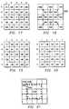
- FIG. 1is a timeline according to the prior art showing one frame period comprised of eight separate sub-frame periods.
- FIG. 2is an array of pixels, having an orthogonal or Manhattan format, showing the location of defective, compensation, and reference pixels.
- FIG. 3is a matrix of intensity values to be displayed on the pixel array of Figure 2.
- FIG. 4is the matrix of the intensity values of Figure 3 that has been modified according to one embodiment of the present invention to minimize the impact of a defective pixel.
- FIG. 5is the matrix of the intensity values of Figure 3 that has been modified according to one embodiment of the present invention to minimize the impact of a defective pixel.
- FIG. 6is a plot of the since function.
- FIG. 7is the matrix of the intensity values of Figure 3 that has been modified according to one embodiment of the present invention to minimize the impact of a defective pixel.
- FIG. 8is the matrix of the intensity values of Figure 3 that has been modified according to one embodiment of the present invention to minimize the impact of a defective pixel.
- FIG. 9is the matrix of the intensity values of Figure 3 that has been modified according to one embodiment of the present invention to minimize the impact of a defective pixel.
- FIG. 10is the matrix of the intensity values of Figure 3 that has been modified according to one embodiment of the present invention to minimize the impact of a defective pixel.
- FIG. 11is the matrix of the intensity values of Figure 3 that has been modified according to one embodiment of the present invention to minimize the impact of a defective pixel.
- FIG. 12is the matrix of the intensity values of Figure 3 that has been modified according to one embodiment of the present invention to minimize the impact of a defective pixel.
- FIG. 13is a matrix of intensity values having an intensity gradient that are to be displayed on the pixel array of Figure 2.
- FIG. 14is the matrix of the intensity values of Figure 13 that has been modified according to one embodiment of the present invention to minimize the impact of a defective pixel.
- FIG. 15is the matrix of the intensity values of Figure 13 that has been modified according to one embodiment of the present invention to minimize the impact of a defective pixel.
- FIG. 16is the matrix of the intensity values of Figure 13 that has been modified according to one embodiment of the present invention to minimize the impact of a defective pixel.
- FIG. 17is the matrix of the intensity values of Figure 13 that has been modified according to one embodiment of the present invention to minimize the impact of a defective pixel.
- FIG. 18is an orthogonal array of pixels showing one possible correspondence between reference pixels and compensation pixels according to one embodiment of the present invention.
- FIG. 19is the matrix of the intensity values of Figure 13 that has been modified according to one embodiment of the present invention to minimize the impact of a defective pixel.
- FIG. 20is the matrix of the intensity values of Figure 13 that has been modified according to one embodiment of the present invention to minimize the impact of a defective pixel.
- FIG. 21is an orthogonal array of pixels showing another possible correspondence between reference pixels and compensation pixels according to one embodiment of the present invention.
- FIG. 22is a matrix of intensity values that has been modified according to one embodiment of the present invention to minimize the impact of three defective pixels.
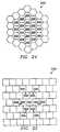
- FIG. 23is an array of pixels, having a staggered, cardinal or brick format, showing the location of defective, compensation, and reference pixels.
- FIG. 24is an array of pixels, having a hexagonal format, showing the location of defective, compensation, and reference pixels.
- FIG. 25is an staggered array of pixels showing one possible correspondence between reference pixels and compensation pixels according to one embodiment of the present invention.
- FIG. 26is an staggered array of pixels showing another possible correspondence between reference pixels and compensation pixels according to one embodiment of the present invention.
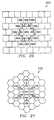
- FIG. 27is an hexagonal array of pixels showing one possible correspondence between reference pixels and compensation pixels according to one embodiment of the present invention.
- FIG. 28is an hexagonal array of pixels showing another possible correspondence between reference pixels and compensation pixels according to one embodiment of the present invention.
- FIG. 29is a block diagram of a display system according to one embodiment of the present invention.
- FIG. 30is a block diagram of a display system according to one embodiment of the present invention including an optical projection path and an optical detector in a feedback path.
- each framerepresents a complete "snapshot" or "frame-grab" of the image being displayed.
- the DMD elements or mirrors of a bistable DMD modulatormay only assume one of two positions, on or off, and the duty cycle of each modulator element within a frame is modulated in order to project gray scale images. Typically this is done by dividing each frame period 100 into multiple sub-frame or "bit-plane" periods 102 , 104 , 106 , 108 as shown in Figure 1.
- bit-planethe data displayed during each bit-plane within a frame is unique. The eye and brain of the viewer tend to integrate the multiple bit-planes to create a frame, much the same way that multiple frames are integrated to achieve the effect of full-motion video.
- bit-planesfrom a binary-encoded word representing the desired intensity of a pixel, or intensity word, is to use each bit of the intensity word to create one bit-plane. Each bit will then control the position of the mirror for one sub-frame or bit-plane. Generally, the time each bit of the intensity word controls the mirror position is doubled for each increase in bit significance. For example, the most significant bit is displayed during sub-frame 102 , the next most significant bit is displayed during sub-frame 104 , the period of which is half as long as the period of sub-frame 102 . Each successive sub-frame is displayed for half the period of the previous sub-frame until all the sub-frames have been displayed.
- FIG. 1shows the sub-frames displayed in order from the most significant 102 to the least significant 108 , practical systems typically do not display the data bits in descending order, nor is each sub-frame period necessarily contiguous. For example, in some display systems, portions of multiple bit planes are displayed simultaneously such that at any given time, different portions of the array are displaying data bits of various significance. Further information on splitting bit-planes is contained in commonly assigned U.S. Patent 5,278,652.
- a selected mirror or pixelhas, during a frame period, the following positions: on, on, off, off, off, on, off, on.
- This sequence of positionscan be represented by the eight bit binary number 11000101 having a decimal equivalent of 197.
- the number 197may be thought of as the grey scale value of the pixel as evaluated by the human eye/brain during the frame. If this same pixel is stuck on, the defect produced thereby will have a continuous grey scale frame value of 255; if it is stuck off, the defect's value will be 0.
- One of the easiest ways of ameliorating the effects of the stuck pixel, or defective pixel 202 , in an array of pixels 200 shown in Figure 2,is to use the pixels 204 surrounding the defective pixel 202 to compensate for the increase, or decrease, in light reflected from the defective pixel 202 .
- the desired intensity for each pixel shown in Figure 2is equal to the corresponding intensity value shown in the matrix of Figure 3.
- each of the 8 pixels 204 surrounding the defective pixel 202is reduced by 9 bit periods, as in the matrix of actual intensity values shown in Figure 4. This results in the total light from the defective pixel 202 and the 8 surrounding pixels 204 being only 3 LSB periods too great as opposed to the original 75 periods. Because the 8 pixels 204 surrounding the defective pixel 202 were used to compensate for the defective pixel 202 , the 8 pixels 204 are referred to as the compensation pixels 204 .
- Figure 5shows the intensity values that are displayed if pixel C3 is stuck off.
- the sinc function waveform 600is characterized as having a central curvilinear portion 602 with a value of 1 and generally symmetrical, positive- and negative-going, damped portions 604 on either side thereof. It was felt that the damped side portions 604 might be related to an appropriate value to be assumed by the compensation pixel. Indeed, it was found that an approximation of the damped side portions is related to a "compensation" value which, if assigned to the compensation pixel 204 , would offset the difference between the actual and desired intensity values of the defective pixel 202, or in the alternative, between the actual intensity value of the defective peel 202 and the intensity value of one or more nearby reference pixels 206 so as to ameliorate the constantly on or constantly off, defective pixel 202.
- the application of this technique and its refinementis another object of the present invention.
- the distance between orthogonally adjacent pixelsis set equal to 3P/2 radians.
- X3P/2 radians and the function evaluates to -0.2122.
- X2 1 ⁇ 2 3P/2 radians and the function evaluates to 0.0558.
- Figure 7is a matrix of the actual intensity values displayed an array of pixels that have the desired intensity shown in Figure 3 when pixel C3 is stuck on.
- Figure 8is the matrix of Figure 7 when pixel C3 is stuck off.
- the average intensity displayed by the 8 compensation pixels 204 and the defective pixel 202is 183 compared to the desired intensity of 180.
- the average intensityis 179.6 compared to the desired intensity of 180.
- the intensity value assigned to the diagonally adjacent compensation pixelsis very close to the intended intensity value of the compensation pixels. Therefore, the diagonally adjacent compensation pixels contribute very little to the compensation of the defective pixel 202 . It is possible to reduce the amount of processing power required and still achieve approximately the same compensation effect by only adjusting the intensity values of the four orthogonally adjacent compensation pixels.
- Figures 9 and 10show the actual displayed intensity values for the matrix of Figure 3 when only the four orthogonally adjacent pixels are used to compensate for a defective pixel 202 that is stuck on ( Figure 9) or off ( Figure 10).
- An alternate method of compensating for a defective pixel according to the present inventionuses the same intensity value for each of the 8 compensation pixels 204 .
- the diagonally adjacent compensation pixelsare assigned the same value as the orthogonally adjacent compensation pixels.
- This methodprovides 8 compensation pixels 204 and only requires the calculation of one compensation value.
- Figures 11 and 12show the actual displayed intensity values, according to this method, for the matrix of Figure 3 when pixel C3 is stuck on ( Figure 11) or off ( Figure 12).
- a second methodinvolves using the actual displayed intensity and the desired intensity of the defective pixel 202 to determine an offset value which is applied to the compensation pixels 204 . While any of the options taught above regarding adjacent and orthogonal compensation pixels 204 may be used in the methods that follow, the examples illustrated will assume that all 8 compensation pixels 204 are treated as orthogonally compensation pixels.
- This second methodhas the advantage of not losing the image information contained in the original intensity value set. While the loss of the information contained in the original compensation intensity values does not alter the displayed image when the desired value for all of the pixels is equal, as in Figure 3, the loss does degrade an image that contained an intensity "edges" or intensity "contour” as shown in Figure 13, especially if the intensity contour was accompanied by image motion between successive image of a video display system.
- Figures 14 and 15show the actual displayed intensity values for the matrix of Figure 13 when the 8 compensation pixels are offset according to the above formula to compensate for a defective pixel 202 that is stuck on ( Figure 14) or off ( Figure 15). As shown in Figures 14 and 15, the compensation pixels 204 maintain the original intensity contour while being offset to compensate for the defective pixel 202 . In Figure 14, the intensity value of each compensation pixel 204 is decreased 27 while in Figure 15, the intensity value of each compensation pixel 204 is increased 27.
- a third methoduses the surrounding reference pixels 206 , that is pixels A1 through A5, B1, B5, C1, C5, D1, D5, and E1 through E5, to calculate either the value of the compensation pixels, or an offset for the compensation pixels 204.
- X nA(B - C) + D n
- Ais the value of the sinc function evaluated for the compensation pixel (-.2122 in this example)
- Bis the actual intensity value of the defective pixel 202
- Cis the average value of the reference pixels 206
- D nis the desired value of the compensation pixel.
- An alternative to this third methoduses the average value of the 16 reference pixels 206 and the desired value of the defective pixel 202 in place of "C" in the above formulas to determine the value of the compensation pixels.
- Figures 16 and 17show the actual displayed intensity values for the matrix of Figure 13 when the 8 compensation pixels 204 are offset according to the above formula, thereby compensating for a defective pixel 202 that is stuck on ( Figure 16) or off ( Figure 17).
- the intensity value of each compensation pixel 204is decreased 20 while in Figure 17, the intensity value of each compensation pixel 204 is increased 34.
- Figure 13shows the desired intensity values for an orthogonal array of pixels 1200 displaying a sharp intensity change between columns 3 and 4.
- pixel C3is stuck on, the previous algorithm calls for decreasing all of the compensation pixels 204 by 20. Because of the distinct edge between columns 3 and 4, averaging all of the reference pixels 206 results in decreasing compensation pixels 204 B2, B3, C2, D2, and D3 too little, and decreasing compensation pixels 204 B4, C4, and D4 too much.
- a fourth method according to the present invention of compensating for defective pixels 102 while preserving edges and contours that may be present in the original intensity value data setinvolves the use of only a portion of the reference pixels 206 when calculating the value or offset for an individual compensation pixel 204 .
- a first methoduses only the reference pixel 1806 that is opposite the defective pixel 1802 with respect to each compensation pixel 1804 .
- the value of reference pixel 1806 A3is used to determine the value of compensation pixel 1804 B3.
- Each arrow 1808 in Figure 18leads from a reference pixel 1806 to a compensation pixel 1804 that is modified by the reference pixel 1806 .
- Application of this first method to the intensity data set shown in Figure 13results in the values shown for the compensation pixels 204 shown in Figure 19 when pixel C3 is stuck on, and shown in Figure 20 when pixel C3 is stuck off.
- any number of pixelsmay be used.
- Figure 21which once again uses arrows 2108 to point from a reference pixel 2106 to a compensation pixel 2104 that it modifies.
- the intensity value of each compensation pixeldepends on the value of three reference pixels 2106 .
- Many other groups of reference pixels 2106may be used to compensate the intensity value of the compensation pixels 2104 , including methods that use as reference pixels those pixels in the area surrounding the reference pixels 2106 , without departing from the methods taught herein.
- Pixels C5 and D6are used to compensate for both pixels D5 and C6, and therefore have a net offset of +76 added to the desired intensity value of 180. Because the examples herein have assumed an 8-bit intensity data word which has a maximum intensity value of 255, the actual intensity value displayed by pixels C5 and D6 is 255 instead of the calculated value of 256.
- the compensation techniques taught hereinare not restricted to the compensation of defective pixels in an orthogonal pixel array, but rather, the techniques may be easily modified and applied to a pixel array of any form.
- the pixel array 2300 of Figure 23has rows of pixels that are staggered or shifted by one-half pixel. This form of array is commonly referred to by several names including: brick-, staggered-, and cardinal-array.
- pixel 2302is assumed to be defective.
- the pixels surrounding the defective pixel 2302are the compensation pixels 2304
- the pixels surrounding the compensation pixels 2304are the reference pixels 2306 .
- a second form of pixel array that may benefit from the methods taught hereinis an array comprised of non-rectangular pixels, for example the array of hexagonal pixels 2400 shown in Figure 24.
- pixel 2402is assumed to be defective.
- the pixels surrounding the defective pixel 2402are the compensation pixels 2404
- the pixels surrounding the compensation pixels 2404are the reference pixels 2406 .
- Figures 25 through 28may easily be applied to non-orthogonal pixel grids as shown in Figures 25 through 28.
- arrowsidentity the reference pixels, associated with each of the compensation pixels.
- Figure 25shows a staggered array of pixels 2500 wherein one reference pixel 2506 is used to determine the offset applied to each compensation pixel 2504 .
- Figure 26shows a staggered array of pixels 2600 wherein three reference pixels 2606 are used to determine the offset applied to each compensation pixel 2604 .
- Figure 27shows a hexagonal array of pixels 2700 wherein one reference pixel 2706 is used to determine the offset applied to each compensation pixel 2704 .
- Figure 28shows a hexagonal array of pixels 2800 wherein three reference pixels 2806 are used to determine the offset applied to each compensation pixel 2804 .
- many other arrangements of reference and compensation pixelsare possible without departing from the present invention.
- the present inventionis also used to compensate for defective or inoperable pixels whose output may be between fully on and fully off.
- a light emitting diode (LED) or liquid crystal device (LCD) displaymay include some pixels that cannot be fully illuminated or darkened, perhaps due to leakage currents in the underlying addressing circuitry. The adjacent pixels are then used to compensate for the inoperable or defective pixel as described above.
- Figure 29is a schematic representation of one example of a display system 2900 according to the present invention.
- Analog video datais sampled by an analog-to-digital converter 2902 and passed to a processor 2904 .
- the processor 2904performs many functions such as data conditioning, gamma correction, deinterlacing, and data formatting, all of which are known in the prior art.
- the processor 2904also calculates and applies the offsets to the compensation pixels according to the present invention.
- the compensated digital video datais then stored in RAM 2906a , 2906b before being driven onto SLM 2908 .
- the processor 2904may use any of the algorithms suggested herein. Which algorithm is selected depends primarily on the amount of processing throughput available and the types of images being displayed. For example, the processor may select an algorithm that uses all of the reference pixels 206 to determine a common value for the compensation pixels when there is image motion in the vicinity of the defective pixel. This algorithm does not require much processing power to implement which is an advantage because the processing power required by other processes may increase when there is scene motion. Furthermore, because the human eye loses a lot of resolution when there is motion in the scene, the viewer is less likely to detect any defects that are generated by a simple compensation algorithm.
- the processordetermines which pixels are defective by reading the contents of the defective pixel map 2910 .
- the locations of the defective pixels 202may be stored in the defective pixel map 2910 when the display is assembled.
- the defective pixel map 2910be periodically updated to include the locations of all pixels that are currently defective.
- a system that is capable of monitoring the operational condition of the pixelsis shown in Figure 30.
- the light 3002 from the SLM 2908passes through a beamsplitter 3004 which allows the majority of the light 3006 to pass through to display screen 3008 .
- detector 3012is a detector array that has a one-to-one correspondence between detector pixels and SLM pixels.
- the processor 2904determines which pixels are defective. While this embodiment uses an expensive detector array 3012, it allows detection of defective pixels in a single image frame.
- An alternative to a system 3000 using a detector array 3012uses a single detector element 3012 to measure the light from the entire image.
- the processor 2904must monitor many frames to data to deduce which pixels are stuck. This second embodiment has the disadvantage of using a lot of processing power to detect the defective pixels.
- a third embodimentuses a single detector element 3012 to locate defective pixels by displaying a dedicated sequence of video test frames. These test frames may be interspersed with the actual image frames at a slow enough rate to be undetectable by the viewer. In television systems, the test frames may be inserted during channel changes. Alternatively, the test frames may be displayed during a self-test routine that is executed whenever the system is turned on prior to displaying actual image data.
- Using a beamsplitter 3004 to direct a portion of the light 3010 to the detectorhas the disadvantage of reducing the amount of fight 3006 that is directed toward the screen 3008 .
- the beamsplitter 3004may be eliminated and the detector 3012 positioned so as to detect light reflected from the screen 3008 .
Landscapes
- Physics & Mathematics (AREA)
- General Physics & Mathematics (AREA)
- Engineering & Computer Science (AREA)
- Optics & Photonics (AREA)
- Computer Hardware Design (AREA)
- Theoretical Computer Science (AREA)
- Control Of Indicators Other Than Cathode Ray Tubes (AREA)
- Mechanical Light Control Or Optical Switches (AREA)
Abstract
Description
- The present invention relates to a method of reducing the visual impact of defects present in a spatial light modulator ("SLM") display, and, more particularly, to a method of ameliorating the visual impact on an observer of improperly operating mirrors of a digital micromirror device (DMD) or deformable mirror device (also DMD) SLM, which improper operation results from one or more mirrors occupying an incorrect position, namely a reflective ("on") position when the proper position is non-reflective ("off') orviceversa.
- There are at least four genera of SLM's: electro-optic, magneto-optic, liquid crystal and DMDs. The latter genus, DMDs, includes a micromechanical array of electronically addressable mirror elements. The mirror elements are reflectors each of which is individually movable. Each mirror is a light reflecting pixel and is capable of mechanical movement in response to an electrical input. Light incident on each mirror may be modulated in its direction (or phase) by reflection from each mirror. To date, DMD SLMs have found use in applications such as optical correlation, spectrum analysis, crossbar switching, frequency excision, display projection, printing and neural networks.
- There are several species of the genus "DMD SLM", including elastomer type, membrane type as well as cantilever-beam, torsion-beam, and flexure-beam types. Selective control, or addressing, of the DMD SLM peels has been achieved by electron-beam input, optically or, as preferred today, by circuitry integrated onto the DMD substrate.
- Each pixel of the DMD SLM array reflects incident light along a path which depends on the position or orientation of the pixel. Typically, each mirror is movable or deflectable between a normal, first position or orientation and one or more second positions or orientations. In only one position, either the normal position or one of the second positions, a mirror directs the incident light along a selected path to a primary light-receiving site, for example, into an optical system and from there onto a viewing surface or a photosensitive drum. In all other pixel positions, incident light is not directed along the selected path to the primary site; rather, it is directed along another path to either a secondary site or to a "light sink" which absorbs or eliminates the light.
- A DMD may take the form of a square, or nearly square, array of mirrors. In this event, the positions of the pixels, each of which is individually controllable by associated addressing facilities, may be altered to generate a video presentation. See commonly assigned US Patents, 5,079,544; 5,061,049; 4,954,789; 4,728,185 and 3,600,798. See also US Patents 4,356,730; 4,229,732; 3,896,338 and 3,886,310. The mirror array may also take other forms, for example, that of a linear array or an array with many more columns than rows, the length of which is much larger than its width. In this latter event, the positions of the mirrors, as determined by their associated addressing facilities, may be altered so that the reflected light prints characters in quasi-line-at-a-time fashion on a photosensitive drum. See commonly assigned US Patents 5,101,236 and 5,041,851. In both events, and in other use environments, appropriate configurations of mirrors enable DMDs to modulate light in amplitude-dominant or phase-dominant modes.
- It has been found convenient to produce integrated addressing circuits monolithically with the mirrors using conventional MOS processing techniques to form the addressing circuits in and on a substrate (e.g., silicon or GaAs) with the mirrors thereabove. The addressing circuits may be planarized and overlain by their respective mirrors to limit light penetration to the circuitry and to minimize the device size. Depending on the device type and the addressing voltages applied, the pixel may be addressed in analog, tristable, or bistable (binary) fashion.
- A membrane type DMD SLM includes a metallized polymer membrane stretched over a spacer grid or other support structure. The openings in the grid define modulator cells or elements which comprise an address electrode and a portion of the polymer membrane supported by the spacer grid. The spacer grid effects an air gap or separation between segments of the membrane and the corresponding underlying addressing electrodes. When an address electrode of an address circuit is energized, by applying a bias voltage to the address electrode, the normally flat related membrane segment is curvilinearly deformed out of its normal, unstretched, planar position by electrostatic attraction between the membrane and the address electrode, and into the air gap where it now acts as a miniature spherical mirror. This deformation stores potential energy in the deformed membrane. When the address electrode is deenergized, the potential energy stored by the membrane returns the membrane to its normal flat position. Incident light reflected by each miniature spherical mirror is concentrated into a relatively narrow cone that is rotationally symmetric about the specularly reflected light. The pixel array can, therefore, be associated with a Schlieren stop, which comprises a single, central obscuration having a position and size to block the image of the light source that results from specular reflection by flat or unmodulated pixels. Modulated or spherically deformed pixels direct a circular patch of light onto the plane of the stop; the patch is centered on, but is larger than, the stop's central obscuration and, therefore, traverses a selected direction and reaches a selected site.
- Membrane DMDs have also been produced by forming an array of relatively thick, separated, flat mirrors supported on a relatively thin polymer membrane above a silicon or other substrate. The underlying addressing circuits formed on and in the substrate are separated by air gaps from their associated pixels when the latter reside in their normal positions. When an addressing circuit is appropriately energized, its mirror or pixel is displaced or deflected toward the substrate by electrostatic attraction. The mirrors remain flat while the membrane immediately surrounding them stretches to permit the mirrors to deflect up-and-down in piston-like fashion. The resultant displacement pattern produces a corresponding phase modulation pattern for the reflected light. This pattern may be converted into analog intensity variations by Schlieren projection techniques or used as the input transducer for an optical information processor. Further information on membrane type DMDs may be obtained from commonly assigned U.S. Patent 4,441,791.
- Beam-type DMDs each comprise a relatively thick (for rigidity) mirror or metal member supported by one or more relatively thin (for compliance), integral beams or springs. Each mirror and its beam(s) is structurally supported above and separated from its associated addressing circuit, and an address or control electrode which is a part of the addressing circuit, by a spacer or support post which supports the beam.
- In the absence of a deflecting force applied to the mirror or metal member, the beam maintains the mirror in a normal, generally horizontal position parallel to the substrate. When the address or control electrode is energized by having a voltage applied thereto by the addressing circuitry, a portion of the mirror aligned with the electrode along the lines of the resulting electrostatic field is electrostatically attracted toward the electrode. Cantilever and/or torsional bending occurs preferentially at the thin beam(s). Such bending stores potential energy in the beam(s) associated with a deflected mirror. The stored potential energy, which tends to return the mirror to its normal position, is effective to return the mirror when the control or address electrode no longer attracts it.
- While the present invention may prove useful relative to all types of SLM's it finds particular utility with beam-type DMDs. Improper operation of these types of DMD's typically involves one or more mirrors of the array becoming "stuck" and remaining in a fixed position regardless of the operation of the applicable addressing circuits. A mirror may become stuck in either the "on" position, the position whereat incident light is reflected onto a viewing surface, or an "off" position, a position whereat incident light is not reflected onto the viewing surface. Pursuant to the foregoing nomenclature, a mirror or pixel which is stuck in the "on" position will continuously reflect light to the viewing surface as a continuous "bright spot," even when the pixel should be "off", i.e. should be transmitting no light to the viewing surface. Moreover, a mirror or pixel which is stuck in the "off" position will not reflect light to the viewing surface, resulting in a continuous "dark spot," even when the pixel should be "on" and transmitting light to the viewing surface. These undesired, improper, bright and dark spots are referred to herein as "defects."
- Defects in DMD displays are, as a minimum, annoying to the viewer. They produce on-going light or dark regions which persist regardless of visual changes occurring to the remainder of the display. At worst, such defects may prevent the display from presenting meaningful visual information. Due to the manner in which DMD SLM's are manufactured, it is not possible to gain access to pixels which are stuck for purposes of rendering them operative. Moreover, pixels which are properly operative when a DMD SLM display is first put into service may later become stuck. The reverse is also possible, that is, previously stuck mirrors may become unstuck. As a consequence, a method of reducing the visual impact of such defects on the viewer to eliminate annoyance and to ensure that meaningful information is presented, which method can be selectively effected on an as-needed basis, and is one object of the present invention.
- According to the present invention there is provided a method of compensating for defects in an image display having an array of pixels, in which each pixel is selectively controllable, which method comprising, identifying a defective pixel, selecting at least one compensation pixel in the vicinity of the defective pixel and controlling the or each pixel such that, in use, a predetermined image intensity is produced over a predetermined image display area.
- The present invention provides a method and display system for reducing the visual impact of defects present in an image display. The display includes an array of pixels, each non-defective pixel being selectively operable in response to input data by addressing facilities between an "on" state, whereat light is directed onto a viewing surface, and an "off" state, whereat light is not directed onto the viewing surface. A defect is the result of a defective pixel which does not respond to the input data presented by the addressing facilities, typically by continuously remaining in its "on" or "off" state. Each defective pixel is immediately surrounded by a first ring of compensation pixels adjacent to the central defective pixel. The compensation pixels are immediately surrounded by a second ring of reference pixels spaced from the central defective pixel. The addressing circuit-determined value of at least one compensation pixel in the first ring surrounding the defective pixel is changed from its desired or intended value, to a corrective value, in order to reduce the visual impact of the defect.
- In one embodiment, the value the compensation pixels is selected such that the average visually detected value for all of the compensation pixels and the defective pixel is equal to the intended value of the defective pixel.
- In another embodiment, the values of the compensation pixels are adjusted by adding an offset to the desired value of each compensation pixel. The offset is chosen such that the sum of the offset values is equal to the intended value of the defective pixel minus the visually detected value of the defective pixel.
- In still another embodiment, a scaling function based on the since function is used to determine the value of, or offset applied to, the compensation pixels.
- According to a further aspect of the present invention there is provided an image display system comprising a modulator having an array of pixels in which each pixel is selectively controllable, means for identifying and selecting at least one compensation pixel in the vicinity of the defective pixel, and a processor for controlling the or each compensation pixel such that in use, a predetermined image intensity is produced over a predetermined image display area.
- In a display system according to one embodiment of the present invention, a modulator comprised of an array of pixels including at least one inoperable pixel and at least one compensation pixel adjacent to the inoperable pixel, receives a set of image data values corresponding to the array of pixels and selectively activates the pixels to represent the set of image data values. A processor receives an image signal and, alter altering the image data value corresponding to said compensation pixel, outputs the set of image data values to the modulator, thereby compensating for the defective pixel.
- FIG. 1 is a timeline according to the prior art showing one frame period comprised of eight separate sub-frame periods.
- FIG. 2 is an array of pixels, having an orthogonal or Manhattan format, showing the location of defective, compensation, and reference pixels.
- FIG. 3 is a matrix of intensity values to be displayed on the pixel array of Figure 2.
- FIG. 4 is the matrix of the intensity values of Figure 3 that has been modified according to one embodiment of the present invention to minimize the impact of a defective pixel.
- FIG. 5 is the matrix of the intensity values of Figure 3 that has been modified according to one embodiment of the present invention to minimize the impact of a defective pixel.
- FIG. 6 is a plot of the since function.
- FIG. 7 is the matrix of the intensity values of Figure 3 that has been modified according to one embodiment of the present invention to minimize the impact of a defective pixel.
- FIG. 8 is the matrix of the intensity values of Figure 3 that has been modified according to one embodiment of the present invention to minimize the impact of a defective pixel.
- FIG. 9 is the matrix of the intensity values of Figure 3 that has been modified according to one embodiment of the present invention to minimize the impact of a defective pixel.
- FIG. 10 is the matrix of the intensity values of Figure 3 that has been modified according to one embodiment of the present invention to minimize the impact of a defective pixel.
- FIG. 11 is the matrix of the intensity values of Figure 3 that has been modified according to one embodiment of the present invention to minimize the impact of a defective pixel.
- FIG. 12 is the matrix of the intensity values of Figure 3 that has been modified according to one embodiment of the present invention to minimize the impact of a defective pixel.
- FIG. 13 is a matrix of intensity values having an intensity gradient that are to be displayed on the pixel array of Figure 2.
- FIG. 14 is the matrix of the intensity values of Figure 13 that has been modified according to one embodiment of the present invention to minimize the impact of a defective pixel.
- FIG. 15 is the matrix of the intensity values of Figure 13 that has been modified according to one embodiment of the present invention to minimize the impact of a defective pixel.
- FIG. 16 is the matrix of the intensity values of Figure 13 that has been modified according to one embodiment of the present invention to minimize the impact of a defective pixel.
- FIG. 17 is the matrix of the intensity values of Figure 13 that has been modified according to one embodiment of the present invention to minimize the impact of a defective pixel.
- FIG. 18 is an orthogonal array of pixels showing one possible correspondence between reference pixels and compensation pixels according to one embodiment of the present invention.
- FIG. 19 is the matrix of the intensity values of Figure 13 that has been modified according to one embodiment of the present invention to minimize the impact of a defective pixel.
- FIG. 20 is the matrix of the intensity values of Figure 13 that has been modified according to one embodiment of the present invention to minimize the impact of a defective pixel.
- FIG. 21 is an orthogonal array of pixels showing another possible correspondence between reference pixels and compensation pixels according to one embodiment of the present invention.
- FIG. 22 is a matrix of intensity values that has been modified according to one embodiment of the present invention to minimize the impact of three defective pixels.
- FIG. 23 is an array of pixels, having a staggered, cardinal or brick format, showing the location of defective, compensation, and reference pixels.
- FIG. 24 is an array of pixels, having a hexagonal format, showing the location of defective, compensation, and reference pixels.
- FIG. 25 is an staggered array of pixels showing one possible correspondence between reference pixels and compensation pixels according to one embodiment of the present invention.
- FIG. 26 is an staggered array of pixels showing another possible correspondence between reference pixels and compensation pixels according to one embodiment of the present invention.
- FIG. 27 is an hexagonal array of pixels showing one possible correspondence between reference pixels and compensation pixels according to one embodiment of the present invention.
- FIG. 28 is an hexagonal array of pixels showing another possible correspondence between reference pixels and compensation pixels according to one embodiment of the present invention.
- FIG. 29 is a block diagram of a display system according to one embodiment of the present invention.
- FIG. 30 is a block diagram of a display system according to one embodiment of the present invention including an optical projection path and an optical detector in a feedback path.
- In one type of DMD display, multiple video images are projected, typically at the rate of 50 to 60 frames per second, in order to give a viewer the effect of true motion. Each frame represents a complete "snapshot" or "frame-grab" of the image being displayed. As discussed earlier, the DMD elements or mirrors of a bistable DMD modulator may only assume one of two positions, on or off, and the duty cycle of each modulator element within a frame is modulated in order to project gray scale images. Typically this is done by dividing each
frame period 100 into multiple sub-frame or "bit-plane"periods - The simplest way to produce bit-planes from a binary-encoded word representing the desired intensity of a pixel, or intensity word, is to use each bit of the intensity word to create one bit-plane. Each bit will then control the position of the mirror for one sub-frame or bit-plane. Generally, the time each bit of the intensity word controls the mirror position is doubled for each increase in bit significance. For example, the most significant bit is displayed during
sub-frame 102, the next most significant bit is displayed duringsub-frame 104, the period of which is half as long as the period ofsub-frame 102. Each successive sub-frame is displayed for half the period of the previous sub-frame until all the sub-frames have been displayed. This causes the integrated displayed intensity to be a linear representation of the intensity word. One sample time-line for an eight-bit display system is shown in Figure 1. Throughout this discussion intensity data values will be represented as eight-bit values, but it should be understood that the methods taught herein are equally applicable to other word lengths. Although Figure 1 shows the sub-frames displayed in order from the most significant102 to the least significant108, practical systems typically do not display the data bits in descending order, nor is each sub-frame period necessarily contiguous. For example, in some display systems, portions of multiple bit planes are displayed simultaneously such that at any given time, different portions of the array are displaying data bits of various significance. Further information on splitting bit-planes is contained in commonly assigned U.S. Patent 5,278,652. - Specifically, assume that a selected mirror or pixel has, during a frame period, the following positions: on, on, off, off, off, on, off, on. This sequence of positions can be represented by the eight bit binary number 11000101 having a decimal equivalent of 197. The number 197 may be thought of as the grey scale value of the pixel as evaluated by the human eye/brain during the frame. If this same pixel is stuck on, the defect produced thereby will have a continuous grey scale frame value of 255; if it is stuck off, the defect's value will be 0.
- Study and analysis of DMD displays have produced some significant observations. First, amelioration of the effect of defects can occur when the condition, on or off, of a mirror in the vicinity of an improperly operating mirror is appropriately adjusted to lessen the visual effect of the defect.
- One of the easiest ways of ameliorating the effects of the stuck pixel, or
defective pixel 202, in an array ofpixels 200 shown in Figure 2, is to use thepixels 204 surrounding thedefective pixel 202 to compensate for the increase, or decrease, in light reflected from thedefective pixel 202. For example, assume that the desired intensity for each pixel shown in Figure 2 is equal to the corresponding intensity value shown in the matrix of Figure 3. In the case shown by Figure 3, the intended intensity value of every pixel is 180. If the intended intensity of thedefective pixel 202 was 180, as shown by element C3 in Figure 3, butpixel 202 was stuck on (intensity = 255), there are 75 bit periods of excess fight in each frame of the display. To reduce the excess light, each of the 8pixels 204 surrounding thedefective pixel 202 is reduced by 9 bit periods, as in the matrix of actual intensity values shown in Figure 4. This results in the total light from thedefective pixel 202 and the 8 surroundingpixels 204 being only 3 LSB periods too great as opposed to the original 75 periods. Because the 8pixels 204 surrounding thedefective pixel 202 were used to compensate for thedefective pixel 202, the 8pixels 204 are referred to as thecompensation pixels 204. Figure 5 shows the intensity values that are displayed if pixel C3 is stuck off. - In an attempt to ascertain what value imposed on the compensation pixel best operates to ameliorate the effect of a defective pixel, analogies were drawn between averaging and the operation of electrical low pass filters, which perform a type of averaging. Various averaging techniques derived from the type of averaging performed by low pass filters were applied to pixel frame values. An effective low pass filter is one which has a so-called sinc function characteristic, that is, the characteristic response which is congruent with the function generated by low pass filtering a unit impulse, which is given by:

defective pixel 202. Thesinc function waveform 600 is characterized as having a centralcurvilinear portion 602 with a value of 1 and generally symmetrical, positive- and negative-going, dampedportions 604 on either side thereof. It was felt that thedamped side portions 604 might be related to an appropriate value to be assumed by the compensation pixel. Indeed, it was found that an approximation of the damped side portions is related to a "compensation" value which, if assigned to thecompensation pixel 204, would offset the difference between the actual and desired intensity values of thedefective pixel 202, or in the alternative, between the actual intensity value of thedefective peel 202 and the intensity value of one or morenearby reference pixels 206 so as to ameliorate the constantly on or constantly off,defective pixel 202. The application of this technique and its refinement is another object of the present invention. - To relate the sinc function to a matrix of pixels, the distance between orthogonally adjacent pixels is set equal to 3P/2 radians. As shown in Figure 6, for orthogonally adjacent compensation pixels,


- There are many ways of implementing a sinc function-shaped correction. The simplest method does not require knowledge of the desired intensity of either the
compensation pixels 204 or thereference pixels 206. According to this first method, the unit impulse response (Y = 1) is assumed to be proportional to the difference between the actual intensity of the defective pixel and the desired intensity of the reference pixel. The intensity of the compensation pixels is then determined according to the following formula:
compensation pixel 204, A is the value of the sinc function evaluated for the compensation pixel, B is the actual intensity value of thedefective pixel 202, and C is the desired intensity value of thedefective pixel 202. For orthogonally adjacent compensation pixels A = -.2122, for diagonally adjacent compensation pixels A = .0558. Figure 7 is a matrix of the actual intensity values displayed an array of pixels that have the desired intensity shown in Figure 3 when pixel C3 is stuck on. Figure 8 is the matrix of Figure 7 when pixel C3 is stuck off. In Figure 7, the average intensity displayed by the 8compensation pixels 204 and thedefective pixel 202 is 183 compared to the desired intensity of 180. In Figure 8, the average intensity is 179.6 compared to the desired intensity of 180. - As can be seen in Figures 7 and 8, the intensity value assigned to the diagonally adjacent compensation pixels is very close to the intended intensity value of the compensation pixels. Therefore, the diagonally adjacent compensation pixels contribute very little to the compensation of the
defective pixel 202. It is possible to reduce the amount of processing power required and still achieve approximately the same compensation effect by only adjusting the intensity values of the four orthogonally adjacent compensation pixels. Figures 9 and 10 show the actual displayed intensity values for the matrix of Figure 3 when only the four orthogonally adjacent pixels are used to compensate for adefective pixel 202 that is stuck on (Figure 9) or off (Figure 10). - An alternate method of compensating for a defective pixel according to the present invention uses the same intensity value for each of the 8
compensation pixels 204. According to this method, the diagonally adjacent compensation pixels are assigned the same value as the orthogonally adjacent compensation pixels. This method provides 8compensation pixels 204 and only requires the calculation of one compensation value. Figures 11 and 12 show the actual displayed intensity values, according to this method, for the matrix of Figure 3 when pixel C3 is stuck on (Figure 11) or off (Figure 12). - While the method thus far determined the value of a compensation pixel by using only the intended or desired intensity value of a
defective pixel 202 and the actual displayed intensity value of thedefective pixel 202, a second method involves using the actual displayed intensity and the desired intensity of thedefective pixel 202 to determine an offset value which is applied to thecompensation pixels 204. While any of the options taught above regarding adjacent andorthogonal compensation pixels 204 may be used in the methods that follow, the examples illustrated will assume that all 8compensation pixels 204 are treated as orthogonally compensation pixels. The difference between the first and second methods is that whereas in the first method the value assigned to thecompensation pixels 204 was determined solely by the desired and actual values of thedefective pixel 202, the second method according to the present invention determines an offset based on the desired and actual values of thedefective pixel 202 and adds this offset to the desired value of the compensation value according to the following formula:
compensation pixel 204, A is the value of the sinc function evaluated for the compensation pixel (-.2122 in this example), B is the actual intensity value of thedefective pixel 202, C is the desired intensity value of thedefective pixel 202, and Dn is the desired value of the compensation pixel. - This second method has the advantage of not losing the image information contained in the original intensity value set. While the loss of the information contained in the original compensation intensity values does not alter the displayed image when the desired value for all of the pixels is equal, as in Figure 3, the loss does degrade an image that contained an intensity "edges" or intensity "contour" as shown in Figure 13, especially if the intensity contour was accompanied by image motion between successive image of a video display system. Figures 14 and 15 show the actual displayed intensity values for the matrix of Figure 13 when the 8 compensation pixels are offset according to the above formula to compensate for a
defective pixel 202 that is stuck on (Figure 14) or off (Figure 15). As shown in Figures 14 and 15, thecompensation pixels 204 maintain the original intensity contour while being offset to compensate for thedefective pixel 202. In Figure 14, the intensity value of eachcompensation pixel 204 is decreased 27 while in Figure 15, the intensity value of eachcompensation pixel 204 is increased 27. - A third method according to the present invention uses the surrounding
reference pixels 206, that is pixels A1 through A5, B1, B5, C1, C5, D1, D5, and E1 through E5, to calculate either the value of the compensation pixels, or an offset for thecompensation pixels 204. To assign a value to the compensation pixels, the following formula is used:
compensation pixel 204, A is the value of the sinc function evaluated for the compensation pixel (-.2122 in this example), B is the actual intensity value of thedefective pixel 202, C is the average value of the 16reference pixels 206, and D is the desired intensity value of thedefective pixel 202. To compensate for adefective pixel 202 by offsetting the compensation pixels, the following formula is used:
compensation pixel 204, A is the value of the sinc function evaluated for the compensation pixel (-.2122 in this example), B is the actual intensity value of thedefective pixel 202, C is the average value of thereference pixels 206, and Dn is the desired value of the compensation pixel. An alternative to this third method uses the average value of the 16reference pixels 206 and the desired value of thedefective pixel 202 in place of "C" in the above formulas to determine the value of the compensation pixels. Figures 16 and 17 show the actual displayed intensity values for the matrix of Figure 13 when the 8compensation pixels 204 are offset according to the above formula, thereby compensating for adefective pixel 202 that is stuck on (Figure 16) or off (Figure 17). In Figure 16, the intensity value of eachcompensation pixel 204 is decreased 20 while in Figure 17, the intensity value of eachcompensation pixel 204 is increased 34. - Although the embodiments taught above help to preserve information from the
original compensation pixels 204. It still has a tendency to lose information contained in thecompensation pixels 204 when there is a significant intensity contour or edge in the displayed image. Figure 13 shows the desired intensity values for an orthogonal array of pixels1200 displaying a sharp intensity change betweencolumns compensation pixels 204 by 20. Because of the distinct edge betweencolumns reference pixels 206 results in decreasingcompensation pixels 204 B2, B3, C2, D2, and D3 too little, and decreasingcompensation pixels 204 B4, C4, and D4 too much. - A fourth method according to the present invention of compensating for
defective pixels 102 while preserving edges and contours that may be present in the original intensity value data set involves the use of only a portion of thereference pixels 206 when calculating the value or offset for anindividual compensation pixel 204. As shown in Figure 18, a first method uses only thereference pixel 1806 that is opposite thedefective pixel 1802 with respect to eachcompensation pixel 1804. For example, only the value ofreference pixel 1806 A3 is used to determine the value ofcompensation pixel 1804 B3. Eacharrow 1808 in Figure 18 leads from areference pixel 1806 to acompensation pixel 1804 that is modified by thereference pixel 1806. Application of this first method to the intensity data set shown in Figure 13 results in the values shown for thecompensation pixels 204 shown in Figure 19 when pixel C3 is stuck on, and shown in Figure 20 when pixel C3 is stuck off. - Although the above example used only a single reference pixel to derive the intensity value of a
compensation pixel 204, any number of pixels may be used. One example is shown in Figure 21 which once again uses arrows2108 to point from areference pixel 2106 to acompensation pixel 2104 that it modifies. As shown in Figure 15, the intensity value of each compensation pixel depends on the value of threereference pixels 2106. Many other groups ofreference pixels 2106 may be used to compensate the intensity value of thecompensation pixels 2104, including methods that use as reference pixels those pixels in the area surrounding thereference pixels 2106, without departing from the methods taught herein. - While the preceding examples have shown the compensation of the effects of
defective pixels 202 that are isolated, it should be understood that the same compensations techniques may be used for multiple defective pixels that are nearby or even adjacent to each other. For example, assume that an image is comprised of a 6x8 array of pixels each with a desired intensity value of 180. Figure 22 shows the actual intensity values displayed assuming pixel C3 is stuck on and pixels D5 and C6 are stuck off. According to the present invention, an offset of -17 is used to compensate for pixel C3 and an offset of +38 is used to compensate for pixels D5 and C6. Pixels C4 and D4 are used to compensate for both pixels C3 and D5. Therefore pixels C4 and D4 have a net offset of +22 added to the desired intensity value of 180. Pixels C5 and D6 are used to compensate for both pixels D5 and C6, and therefore have a net offset of +76 added to the desired intensity value of 180. Because the examples herein have assumed an 8-bit intensity data word which has a maximum intensity value of 255, the actual intensity value displayed by pixels C5 and D6 is 255 instead of the calculated value of 256. - The compensation techniques taught herein are not restricted to the compensation of defective pixels in an orthogonal pixel array, but rather, the techniques may be easily modified and applied to a pixel array of any form. For example, the
pixel array 2300 of Figure 23 has rows of pixels that are staggered or shifted by one-half pixel. This form of array is commonly referred to by several names including: brick-, staggered-, and cardinal-array. In Figure 23,pixel 2302 is assumed to be defective. According to the present invention, the pixels surrounding thedefective pixel 2302 are thecompensation pixels 2304, and the pixels surrounding thecompensation pixels 2304 are thereference pixels 2306. - A second form of pixel array that may benefit from the methods taught herein is an array comprised of non-rectangular pixels, for example the array of
hexagonal pixels 2400 shown in Figure 24. In Figure 24,pixel 2402 is assumed to be defective. Once again, the pixels surrounding thedefective pixel 2402 are thecompensation pixels 2404, and the pixels surrounding thecompensation pixels 2404 are thereference pixels 2406. - The use of a subset of the
reference pixels 206 to determine the offset for acompensation pixel 204, as taught herein, may easily be applied to non-orthogonal pixel grids as shown in Figures 25 through 28. In each of Figures 25 through 28, arrows identity the reference pixels, associated with each of the compensation pixels. Figure 25 shows a staggered array ofpixels 2500 wherein onereference pixel 2506 is used to determine the offset applied to eachcompensation pixel 2504. Figure 26 shows a staggered array ofpixels 2600 wherein threereference pixels 2606 are used to determine the offset applied to eachcompensation pixel 2604. Figure 27 shows a hexagonal array ofpixels 2700 wherein onereference pixel 2706 is used to determine the offset applied to eachcompensation pixel 2704. Figure 28 shows a hexagonal array ofpixels 2800 wherein threereference pixels 2806 are used to determine the offset applied to eachcompensation pixel 2804. As stated above, many other arrangements of reference and compensation pixels are possible without departing from the present invention. - Although the examples used to describe the present invention have thus far referred to the defective pixel as being either stuck on or stuck off, it should be understood that the present invention is also used to compensate for defective or inoperable pixels whose output may be between fully on and fully off. For example, a light emitting diode (LED) or liquid crystal device (LCD) display may include some pixels that cannot be fully illuminated or darkened, perhaps due to leakage currents in the underlying addressing circuitry. The adjacent pixels are then used to compensate for the inoperable or defective pixel as described above.
- Figure 29 is a schematic representation of one example of a
display system 2900 according to the present invention. Analog video data is sampled by an analog-to-digital converter 2902 and passed to aprocessor 2904. Theprocessor 2904 performs many functions such as data conditioning, gamma correction, deinterlacing, and data formatting, all of which are known in the prior art. In addition to the existing functions performed by theprocessor 2904, theprocessor 2904 also calculates and applies the offsets to the compensation pixels according to the present invention. The compensated digital video data is then stored inRAM 2906a,2906b before being driven ontoSLM 2908. - To compensate for the
defective pixels 202, theprocessor 2904 may use any of the algorithms suggested herein. Which algorithm is selected depends primarily on the amount of processing throughput available and the types of images being displayed. For example, the processor may select an algorithm that uses all of thereference pixels 206 to determine a common value for the compensation pixels when there is image motion in the vicinity of the defective pixel. This algorithm does not require much processing power to implement which is an advantage because the processing power required by other processes may increase when there is scene motion. Furthermore, because the human eye loses a lot of resolution when there is motion in the scene, the viewer is less likely to detect any defects that are generated by a simple compensation algorithm. - The processor determines which pixels are defective by reading the contents of the
defective pixel map 2910. The locations of thedefective pixels 202 may be stored in thedefective pixel map 2910 when the display is assembled. However, as mentioned above regarding DMDs, there is a tendency for pixels to either become unstuck, or to become stuck, during the operation of the DMD. Compensation of intermittently defective pixels requires that thedefective pixel map 2910 be periodically updated to include the locations of all pixels that are currently defective. A system that is capable of monitoring the operational condition of the pixels is shown in Figure 30. In Figure 30, the light3002 from theSLM 2908 passes through abeamsplitter 3004 which allows the majority of the light3006 to pass through to displayscreen 3008. A small portion of the light3010 is directed by thebeam splitter 3004 toward thedetector 3012. In a first detection embodiment,detector 3012 is a detector array that has a one-to-one correspondence between detector pixels and SLM pixels. By monitoring the output of thedetector array 3012, while images were being displayed, theprocessor 2904 determines which pixels are defective. While this embodiment uses anexpensive detector array 3012, it allows detection of defective pixels in a single image frame. An alternative to asystem 3000 using adetector array 3012 uses asingle detector element 3012 to measure the light from the entire image. In this second detection embodiment, theprocessor 2904 must monitor many frames to data to deduce which pixels are stuck. This second embodiment has the disadvantage of using a lot of processing power to detect the defective pixels. A third embodiment uses asingle detector element 3012 to locate defective pixels by displaying a dedicated sequence of video test frames. These test frames may be interspersed with the actual image frames at a slow enough rate to be undetectable by the viewer. In television systems, the test frames may be inserted during channel changes. Alternatively, the test frames may be displayed during a self-test routine that is executed whenever the system is turned on prior to displaying actual image data. - Using a
beamsplitter 3004 to direct a portion of the light3010 to the detector has the disadvantage of reducing the amount offight 3006 that is directed toward thescreen 3008. To avoid reducing the light3006 directed toward thescreen 3008, thebeamsplitter 3004 may be eliminated and thedetector 3012 positioned so as to detect light reflected from thescreen 3008. - Thus, although there has been disclosed to this point a particular embodiment for a method of reducing the visual impact of defects present in a spatial light modulator display, it is not intended that such specific references be considered as limitations upon the scope of this invention except in-so-far as set forth in the following claims. Furthermore, having described the invention in connection with certain specific embodiments thereof, it is to be understood that further modifications and permutations may now suggest themselves to those skilled in the art, it is intended to cover all such modifications and permutations as fall within the scope of the appended claims.


Claims (12)
- A method of compensating for defects in an image display having an array of pixels and each pixel being selectively controllable, which method comprising:
identifying a defective pixel;
selecting at least one compensation pixel in the vicinity of the defective pixel;
controlling the or each compensation pixel such that, in use, a predetermined image intensity is produced over a predetermined image display area. - A method of compensating for defects present in an image display, having an array of pixels, each pixel being selectively controllable; each defective pixel being, immediately surrounded by a first ring of compensation pixels adjacent to the defective pixel; which method comprising:
identifying a defective pixel; and
changing an image data value of at least one compensation pixel in the first ring surrounding the defective pixel to a corrective value given by:
CSINC is a value of the sinc function evaluated for the compensation pixel,
DACT is a detected intensity value of the defective pixel, and DINT is a desired intensity value of the defective pixel. - A method of compensating for defects present in an image display, having an array of pixels, each pixel being selectively controllable; each defective pixel being, immediately surrounded by a first ring of compensation pixels adjacent to the defective pixel, the first ring of compensation pixels being immediately surrounded by a second ring of reference pixels spaced from the defective pixel; which method comprising:
identifying a defective pixel; and
changing an image data value of at least one compensation pixel in the first ring surrounding the defective pixel to a corrective value, given by:
- The method of Claims 2 - 3, wherein the identifying step is effected by comparing the actual light directed onto a viewing screen by the defective pixel and the desired intensity value of the defective pixel.
- The method of Claims 2 - 4, further comprising the step of storing the location of the defective pixels in a memory.
- The method of Claim 3 - 5, further comprising replacing:
DINT, the desired intensity value of the defective pixel, with CORG, the original value of the compensation pixel. - An image display system comprising:
a modulator having an array of pixels, each pixel being selectively controllable:
means for identifying a defective pixel and selecting at least one compensation pixel in the vicinity of the defective pixel;
a processor for controlling the or each compensation pixel such that, in use, a predetermined image intensity is produced over a predetermined image display area. - An image display system comprising:
a modulator having an array of pixels and arranged to receive a set of image data values and for selectively controlling each pixel;
means for detecting the location of a defective pixel and for selecting at least one compensation pixel in the vicinity of the defective pixel; and
a processor for receiving an image signal and generating a set of image data values for the modulator, wherein the processor changes the image data value of the or each compensation pixel to a corrective value given by:
- An image display system comprising:
a modulator having an array of pixels and arranged to receive a set of image data values and for selectively controlling each pixel;
means for detecting the location of a defective pixel, for selecting at least one compensation pixel in the vicinity of the defective pixel, and for selecting one or more reference pixel adjacent to the or each compensation pixel and spaced apart from said defective pixel; and
a processor for receiving an image signal and generating a set of image data values for the modulator, wherein the processor changes the image data value of the or each compensation pixelto a corrective value given by:
- The display system of Claims 8 - 9, further comprising a memory containing the locations of defective pixels, wherein said memory communicates the locations of the defective pixels to the processor.
- The display system of Claims 8 - 10, wherein said means for detecting communicates the locations of the defective pixels to the processor.
- The display system of Claim 11, wherein the means for detecting the locations of the defective pixels is a camera.


Applications Claiming Priority (2)
| Application Number | Priority Date | Filing Date | Title |
|---|---|---|---|
| US08/275,057US5504504A (en) | 1994-07-13 | 1994-07-13 | Method of reducing the visual impact of defects present in a spatial light modulator display |
| US275057 | 1994-07-13 |
Publications (3)
| Publication Number | Publication Date |
|---|---|
| EP0692728A2true EP0692728A2 (en) | 1996-01-17 |
| EP0692728A3 EP0692728A3 (en) | 1997-06-04 |
| EP0692728B1 EP0692728B1 (en) | 2002-10-16 |
Family
ID=23050708
Family Applications (1)
| Application Number | Title | Priority Date | Filing Date |
|---|---|---|---|
| EP95110980AExpired - LifetimeEP0692728B1 (en) | 1994-07-13 | 1995-07-13 | Improvements in and relating to spatial light modulators |
Country Status (6)
| Country | Link |
|---|---|
| US (1) | US5504504A (en) |
| EP (1) | EP0692728B1 (en) |
| JP (1) | JP3810107B2 (en) |
| KR (1) | KR100346879B1 (en) |
| DE (1) | DE69528554T2 (en) |
| TW (1) | TW319860B (en) |
Cited By (11)
| Publication number | Priority date | Publication date | Assignee | Title |
|---|---|---|---|---|
| EP0887681A3 (en)* | 1997-06-26 | 2000-01-26 | Xerox Corporation | Fault tolerant projective display having redundant light modulators |
| EP1416462A1 (en)* | 2002-10-31 | 2004-05-06 | Hewlett-Packard Development Company, L.P. | Projection system utilising SLM pixels that include SLM pixel regions satisfying acceptable defective SLM pixel policy and SLM pixel regions failing policy |
| EP1605313A3 (en)* | 2004-06-08 | 2006-04-05 | ASML Netherlands BV | Lithographic apparatus and device manufacturing method |
| EP1553548A3 (en)* | 2003-12-31 | 2006-05-10 | Hewlett-Packard Development Company, L.P. | Method and apparatus for displaying an image with a display having a set of defective pixels |
| WO2008033760A3 (en)* | 2006-09-13 | 2008-05-08 | Hewlett Packard Development Co | Masking a visual defect |
| WO2010092189A1 (en)* | 2009-02-16 | 2010-08-19 | Micronic Laser Systems Ab | Reconfigurable micro-mechanical light modulator and method |
| EP2301009A1 (en)* | 2008-07-15 | 2011-03-30 | Barco NV | Method for processing an image in a display |
| CN106206654A (en)* | 2015-05-26 | 2016-12-07 | 三星显示有限公司 | Display device |
| CN110910807A (en)* | 2018-09-17 | 2020-03-24 | 苹果公司 | Correction of defective memory for in-pixel memory displays |
| US11378840B2 (en) | 2002-03-13 | 2022-07-05 | Dolby Laboratories Licensing Corporation | Image display |
| US11676558B2 (en) | 2017-01-20 | 2023-06-13 | Semiconductor Energy Laboratory Co., Ltd. | Display system and electronic device |
Families Citing this family (125)
| Publication number | Priority date | Publication date | Assignee | Title |
|---|---|---|---|---|
| US6219015B1 (en) | 1992-04-28 | 2001-04-17 | The Board Of Directors Of The Leland Stanford, Junior University | Method and apparatus for using an array of grating light valves to produce multicolor optical images |
| KR0147939B1 (en)* | 1994-11-11 | 1998-09-15 | 배순훈 | Pixel correction apparatus of projector |
| US6025818A (en)* | 1994-12-27 | 2000-02-15 | Pioneer Electronic Corporation | Method for correcting pixel data in a self-luminous display panel driving system |
| US5617242A (en)* | 1995-01-10 | 1997-04-01 | Texas Instruments Incorporated | Repair of digital micromirror device having white defects |
| US5717513A (en)* | 1995-01-10 | 1998-02-10 | Texas Instruments Incorporated | Unsticking mirror elements of digital micromirror device |
| US5841579A (en) | 1995-06-07 | 1998-11-24 | Silicon Light Machines | Flat diffraction grating light valve |
| US6969635B2 (en)* | 2000-12-07 | 2005-11-29 | Reflectivity, Inc. | Methods for depositing, releasing and packaging micro-electromechanical devices on wafer substrates |
| US5821915A (en)* | 1995-10-11 | 1998-10-13 | Hewlett-Packard Company | Method and apparatus for removing artifacts from scanned halftone images |
| JP3519853B2 (en)* | 1996-02-28 | 2004-04-19 | 富士写真フイルム株式会社 | Micromirror image forming apparatus and management method thereof |
| US6697037B1 (en)* | 1996-04-29 | 2004-02-24 | International Business Machines Corporation | TFT LCD active data line repair |
| JPH09314910A (en)* | 1996-05-30 | 1997-12-09 | Fuji Photo Film Co Ltd | Color printer |
| DE19622314A1 (en)* | 1996-06-04 | 1997-12-11 | Sel Alcatel Ag | Telecommunication terminal and device for projecting visually detectable information |
| JP3333686B2 (en)* | 1996-06-28 | 2002-10-15 | 松下電器産業株式会社 | Display screen inspection method |
| US5982553A (en) | 1997-03-20 | 1999-11-09 | Silicon Light Machines | Display device incorporating one-dimensional grating light-valve array |
| US5774254A (en)* | 1997-06-26 | 1998-06-30 | Xerox Corporation | Fault tolerant light modulator display system |
| US5790297A (en)* | 1997-06-26 | 1998-08-04 | Xerox Corporation | Optical row displacement for a fault tolerant projective display |
| US6088102A (en) | 1997-10-31 | 2000-07-11 | Silicon Light Machines | Display apparatus including grating light-valve array and interferometric optical system |
| EP0933925A3 (en)* | 1997-12-31 | 2002-06-26 | Texas Instruments Inc. | Photofinishing utilizing modulated light source array |
| SE9800665D0 (en)* | 1998-03-02 | 1998-03-02 | Micronic Laser Systems Ab | Improved method for projection printing using a micromirror SLM |
| US6271808B1 (en) | 1998-06-05 | 2001-08-07 | Silicon Light Machines | Stereo head mounted display using a single display device |
| US6130770A (en) | 1998-06-23 | 2000-10-10 | Silicon Light Machines | Electron gun activated grating light valve |
| US6101036A (en) | 1998-06-23 | 2000-08-08 | Silicon Light Machines | Embossed diffraction grating alone and in combination with changeable image display |
| US6215579B1 (en) | 1998-06-24 | 2001-04-10 | Silicon Light Machines | Method and apparatus for modulating an incident light beam for forming a two-dimensional image |
| US6303986B1 (en) | 1998-07-29 | 2001-10-16 | Silicon Light Machines | Method of and apparatus for sealing an hermetic lid to a semiconductor die |
| US6872984B1 (en) | 1998-07-29 | 2005-03-29 | Silicon Light Machines Corporation | Method of sealing a hermetic lid to a semiconductor die at an angle |
| US6208327B1 (en)* | 1998-07-31 | 2001-03-27 | International Business Machines Corporation | Camouflage of imaged post spacers and compensation of pixels that depart from nominal operating conditions by luminance diffusion |
| US6246185B1 (en)* | 1998-12-31 | 2001-06-12 | Texas Instruments Incorporated | High frequency ballast for high intensity discharge lamps |
| TW575855B (en)* | 1999-08-05 | 2004-02-11 | Sharp Kk | Display device |
| US6359662B1 (en)* | 1999-11-05 | 2002-03-19 | Agilent Technologies, Inc. | Method and system for compensating for defects in a multi-light valve display system |
| US6618115B1 (en)* | 1999-11-19 | 2003-09-09 | Semiconductor Energy Laboratory Co., Ltd. | Defective pixel compensation system and display device using the system |
| JP4754682B2 (en)* | 1999-11-19 | 2011-08-24 | 株式会社半導体エネルギー研究所 | Display device |
| US6792159B1 (en)* | 1999-12-29 | 2004-09-14 | Ge Medical Systems Global Technology Company, Llc | Correction of defective pixels in a detector using temporal gradients |
| US7068854B1 (en)* | 1999-12-29 | 2006-06-27 | Ge Medical Systems Global Technology Company, Llc | Correction of defective pixels in a detector |
| US6956878B1 (en) | 2000-02-07 | 2005-10-18 | Silicon Light Machines Corporation | Method and apparatus for reducing laser speckle using polarization averaging |
| US7006275B2 (en)* | 2000-08-30 | 2006-02-28 | Reflectivity, Inc | Packaged micromirror array for a projection display |
| EP1390806B1 (en)* | 2001-02-27 | 2010-08-25 | Dolby Laboratories Licensing Corporation | High dynamic range display devices |
| US20020122237A1 (en)* | 2001-03-01 | 2002-09-05 | Torbjorn Sandstrom | Method and apparatus for spatial light modulation |
| US7177081B2 (en) | 2001-03-08 | 2007-02-13 | Silicon Light Machines Corporation | High contrast grating light valve type device |
| US6707591B2 (en) | 2001-04-10 | 2004-03-16 | Silicon Light Machines | Angled illumination for a single order light modulator based projection system |
| US6865346B1 (en) | 2001-06-05 | 2005-03-08 | Silicon Light Machines Corporation | Fiber optic transceiver |
| US6747781B2 (en) | 2001-06-25 | 2004-06-08 | Silicon Light Machines, Inc. | Method, apparatus, and diffuser for reducing laser speckle |
| US6782205B2 (en) | 2001-06-25 | 2004-08-24 | Silicon Light Machines | Method and apparatus for dynamic equalization in wavelength division multiplexing |
| US7023606B2 (en)* | 2001-08-03 | 2006-04-04 | Reflectivity, Inc | Micromirror array for projection TV |
| US6829092B2 (en) | 2001-08-15 | 2004-12-07 | Silicon Light Machines, Inc. | Blazed grating light valve |
| CN1582407A (en) | 2001-09-12 | 2005-02-16 | 麦克罗尼克激光系统公司 | Improved methods and apparatus using spatial light modulators |
| US7302111B2 (en)* | 2001-09-12 | 2007-11-27 | Micronic Laser Systems A.B. | Graphics engine for high precision lithography |
| US6930364B2 (en) | 2001-09-13 | 2005-08-16 | Silicon Light Machines Corporation | Microelectronic mechanical system and methods |
| US6958785B2 (en)* | 2001-10-22 | 2005-10-25 | Eastman Kodak Company | Method and apparatus for determining and correcting for illumination variations in a digital projector |
| US6956995B1 (en) | 2001-11-09 | 2005-10-18 | Silicon Light Machines Corporation | Optical communication arrangement |
| US6618185B2 (en)* | 2001-11-28 | 2003-09-09 | Micronic Laser Systems Ab | Defective pixel compensation method |
| US20030233630A1 (en)* | 2001-12-14 | 2003-12-18 | Torbjorn Sandstrom | Methods and systems for process control of corner feature embellishment |
| SE0104238D0 (en)* | 2001-12-14 | 2001-12-14 | Micronic Laser Systems Ab | Method and apparatus for patterning a workpiece |
| US7106490B2 (en)* | 2001-12-14 | 2006-09-12 | Micronic Laser Systems Ab | Methods and systems for improved boundary contrast |
| US6800238B1 (en) | 2002-01-15 | 2004-10-05 | Silicon Light Machines, Inc. | Method for domain patterning in low coercive field ferroelectrics |
| US8687271B2 (en) | 2002-03-13 | 2014-04-01 | Dolby Laboratories Licensing Corporation | N-modulation displays and related methods |
| US6728023B1 (en) | 2002-05-28 | 2004-04-27 | Silicon Light Machines | Optical device arrays with optimized image resolution |
| US6767751B2 (en) | 2002-05-28 | 2004-07-27 | Silicon Light Machines, Inc. | Integrated driver process flow |
| US7054515B1 (en) | 2002-05-30 | 2006-05-30 | Silicon Light Machines Corporation | Diffractive light modulator-based dynamic equalizer with integrated spectral monitor |
| US6822797B1 (en) | 2002-05-31 | 2004-11-23 | Silicon Light Machines, Inc. | Light modulator structure for producing high-contrast operation using zero-order light |
| US7202894B2 (en)* | 2002-06-04 | 2007-04-10 | Micron Technology, Inc. | Method and apparatus for real time identification and correction of pixel defects for image sensor arrays |
| US6829258B1 (en) | 2002-06-26 | 2004-12-07 | Silicon Light Machines, Inc. | Rapidly tunable external cavity laser |
| US6714337B1 (en) | 2002-06-28 | 2004-03-30 | Silicon Light Machines | Method and device for modulating a light beam and having an improved gamma response |
| US6813059B2 (en) | 2002-06-28 | 2004-11-02 | Silicon Light Machines, Inc. | Reduced formation of asperities in contact micro-structures |
| US6908201B2 (en) | 2002-06-28 | 2005-06-21 | Silicon Light Machines Corporation | Micro-support structures |
| US7057795B2 (en) | 2002-08-20 | 2006-06-06 | Silicon Light Machines Corporation | Micro-structures with individually addressable ribbon pairs |
| US6801354B1 (en) | 2002-08-20 | 2004-10-05 | Silicon Light Machines, Inc. | 2-D diffraction grating for substantially eliminating polarization dependent losses |
| US6712480B1 (en) | 2002-09-27 | 2004-03-30 | Silicon Light Machines | Controlled curvature of stressed micro-structures |
| US6928207B1 (en) | 2002-12-12 | 2005-08-09 | Silicon Light Machines Corporation | Apparatus for selectively blocking WDM channels |
| US6987600B1 (en) | 2002-12-17 | 2006-01-17 | Silicon Light Machines Corporation | Arbitrary phase profile for better equalization in dynamic gain equalizer |
| US7057819B1 (en) | 2002-12-17 | 2006-06-06 | Silicon Light Machines Corporation | High contrast tilting ribbon blazed grating |
| US6934070B1 (en) | 2002-12-18 | 2005-08-23 | Silicon Light Machines Corporation | Chirped optical MEM device |
| US6927891B1 (en) | 2002-12-23 | 2005-08-09 | Silicon Light Machines Corporation | Tilt-able grating plane for improved crosstalk in 1×N blaze switches |
| JP2006516724A (en)* | 2003-01-15 | 2006-07-06 | マイクロニック レーザー システムズ アクチボラゲット | How to detect defective pixels |
| US7068372B1 (en) | 2003-01-28 | 2006-06-27 | Silicon Light Machines Corporation | MEMS interferometer-based reconfigurable optical add-and-drop multiplexor |
| US7286764B1 (en) | 2003-02-03 | 2007-10-23 | Silicon Light Machines Corporation | Reconfigurable modulator-based optical add-and-drop multiplexer |
| US6947613B1 (en) | 2003-02-11 | 2005-09-20 | Silicon Light Machines Corporation | Wavelength selective switch and equalizer |
| US7042622B2 (en)* | 2003-10-30 | 2006-05-09 | Reflectivity, Inc | Micromirror and post arrangements on substrates |
| US6922272B1 (en) | 2003-02-14 | 2005-07-26 | Silicon Light Machines Corporation | Method and apparatus for leveling thermal stress variations in multi-layer MEMS devices |
| US7391973B1 (en) | 2003-02-28 | 2008-06-24 | Silicon Light Machines Corporation | Two-stage gain equalizer |
| US6922273B1 (en) | 2003-02-28 | 2005-07-26 | Silicon Light Machines Corporation | PDL mitigation structure for diffractive MEMS and gratings |
| US6806997B1 (en) | 2003-02-28 | 2004-10-19 | Silicon Light Machines, Inc. | Patterned diffractive light modulator ribbon for PDL reduction |
| US7027202B1 (en) | 2003-02-28 | 2006-04-11 | Silicon Light Machines Corp | Silicon substrate as a light modulator sacrificial layer |
| US6829077B1 (en) | 2003-02-28 | 2004-12-07 | Silicon Light Machines, Inc. | Diffractive light modulator with dynamically rotatable diffraction plane |
| US7042611B1 (en) | 2003-03-03 | 2006-05-09 | Silicon Light Machines Corporation | Pre-deflected bias ribbons |
| US7212359B2 (en)* | 2003-07-25 | 2007-05-01 | Texas Instruments Incorporated | Color rendering of illumination light in display systems |
| US7131762B2 (en)* | 2003-07-25 | 2006-11-07 | Texas Instruments Incorporated | Color rendering of illumination light in display systems |
| US6888521B1 (en) | 2003-10-30 | 2005-05-03 | Reflectivity, Inc | Integrated driver for use in display systems having micromirrors |
| EP1536399A1 (en) | 2003-11-26 | 2005-06-01 | Barco N.V. | Method and device for visual masking of defects in matrix displays by using characteristics of the human vision system |
| US7133118B2 (en)* | 2004-02-18 | 2006-11-07 | Asml Netherlands, B.V. | Lithographic apparatus and device manufacturing method |
| EP1719018A1 (en)* | 2004-02-25 | 2006-11-08 | Micronic Laser Systems Ab | Methods for exposing patterns and emulating masks in optical maskless lithography |
| US8872869B2 (en)* | 2004-11-23 | 2014-10-28 | Hewlett-Packard Development Company, L.P. | System and method for correcting defective pixels of a display device |
| US7253881B2 (en)* | 2004-12-29 | 2007-08-07 | Asml Netherlands Bv | Methods and systems for lithographic gray scaling |
| US7292024B2 (en) | 2005-04-28 | 2007-11-06 | Avago Technologies Ecbu Ip (Singapore) Pte Ltd | Defect mitigation in display panels |
| US7593026B2 (en)* | 2005-05-11 | 2009-09-22 | L-3 Communications Corporation | Dynamic display optimization method and system with image motion |
| US9318053B2 (en)* | 2005-07-04 | 2016-04-19 | Semiconductor Energy Laboratory Co., Ltd. | Semiconductor device and driving method thereof |
| US8044944B2 (en)* | 2005-07-22 | 2011-10-25 | Nvidia Corporation | Defective pixel management for flat panel displays |
| US20070081739A1 (en)* | 2005-10-11 | 2007-04-12 | International Business Machines Corporation | Modifying text or images when defect pixels are found on a display |
| KR101127843B1 (en)* | 2005-10-25 | 2012-03-21 | 엘지디스플레이 주식회사 | Flat Display Apparatus And Picture Quality Controling Method Thereof |
| US7948506B2 (en)* | 2005-11-15 | 2011-05-24 | Global Oled Technology Llc | Method and apparatus for defect correction in a display |
| KR101186049B1 (en) | 2005-12-02 | 2012-09-25 | 엘지디스플레이 주식회사 | Flat Display Panel, Fabricating Method thereof, Fabricating Apparatus thereof, Picture Quality Controlling Method thereof, Picture Quality Controlling Apparatus |
| KR101127829B1 (en)* | 2005-12-07 | 2012-03-20 | 엘지디스플레이 주식회사 | Flat Display Panel, Manufacturing Method thereof, Manufacturing Apparatus thereof, Picture Quality Controlling Apparatus thereof and Picture Quality Controlling Method thereof |
| US7460133B2 (en) | 2006-04-04 | 2008-12-02 | Sharp Laboratories Of America, Inc. | Optimal hiding for defective subpixels |
| US20070257866A1 (en)* | 2006-05-08 | 2007-11-08 | Eastman Kodak Company | Method and apparatus for defect correction in a display |
| KR101255311B1 (en)* | 2006-06-29 | 2013-04-15 | 엘지디스플레이 주식회사 | Flat Panel Display and Method of Controlling Picture Quality thereof |
| US20080117231A1 (en)* | 2006-11-19 | 2008-05-22 | Tom Kimpe | Display assemblies and computer programs and methods for defect compensation |
| US8994757B2 (en)* | 2007-03-15 | 2015-03-31 | Scalable Display Technologies, Inc. | System and method for providing improved display quality by display adjustment and image processing using optical feedback |
| US7920751B2 (en)* | 2007-03-16 | 2011-04-05 | General Electric Company | Adaptive gradient weighting technique for detector bad cell correction |
| JP2009047965A (en)* | 2007-08-21 | 2009-03-05 | Seiko Epson Corp | Image processing apparatus, image processing method, display apparatus, and program |
| US20090135279A1 (en)* | 2007-11-26 | 2009-05-28 | Xerox Corporation | Reducing imaging artifacts caused by defective imaging element |
| US7551341B1 (en)* | 2008-01-28 | 2009-06-23 | Dolby Laboratories Licensing Corporation | Serial modulation display having binary light modulation stage |
| WO2009130603A2 (en)* | 2008-04-24 | 2009-10-29 | Micronic Laser Systems Ab | Spatial light modulator with structured mirror surfaces |
| WO2009156129A1 (en)* | 2008-06-24 | 2009-12-30 | Carl Zeiss Ag | Projector and method for projecting an image |
| US20090322800A1 (en) | 2008-06-25 | 2009-12-31 | Dolby Laboratories Licensing Corporation | Method and apparatus in various embodiments for hdr implementation in display devices |
| JP5302915B2 (en)* | 2009-03-18 | 2013-10-02 | パナソニック株式会社 | Organic EL display device and control method |
| JP2011107410A (en)* | 2009-11-17 | 2011-06-02 | Sony Corp | Image display device and image display method |
| US8539395B2 (en) | 2010-03-05 | 2013-09-17 | Micronic Laser Systems Ab | Method and apparatus for merging multiple geometrical pixel images and generating a single modulator pixel image |
| US8619164B2 (en) | 2010-06-22 | 2013-12-31 | Lockheed Martin Corporation | Complementary pixel reconstruction |
| KR101958434B1 (en)* | 2011-09-05 | 2019-03-15 | 삼성디스플레이 주식회사 | Organic light emitting diode display |
| JP2014010859A (en)* | 2012-06-29 | 2014-01-20 | Hitachi Consumer Electronics Co Ltd | Method and device for recording and reproducing optical information |
| JP2015007739A (en)* | 2012-10-01 | 2015-01-15 | キヤノン株式会社 | Display divice and control method thereof |
| KR102328841B1 (en) | 2014-12-24 | 2021-11-19 | 엘지디스플레이 주식회사 | Organic light emitting display device and driving method thereof |
| DE102015100859A1 (en)* | 2015-01-21 | 2016-07-21 | Osram Oled Gmbh | Method for operating a display device and display device |
| KR102533385B1 (en)* | 2018-01-31 | 2023-05-17 | 엘지전자 주식회사 | Control device |
| DE102018208417A1 (en) | 2018-05-28 | 2019-11-28 | Fraunhofer-Gesellschaft zur Förderung der angewandten Forschung e.V. | Projection device and projection method |
| JP2022025979A (en)* | 2020-07-30 | 2022-02-10 | 京セラ株式会社 | Luminance correction device for light emission display device |
Citations (13)
| Publication number | Priority date | Publication date | Assignee | Title |
|---|---|---|---|---|
| US3600798A (en) | 1969-02-25 | 1971-08-24 | Texas Instruments Inc | Process for fabricating a panel array of electromechanical light valves |
| US3886310A (en) | 1973-08-22 | 1975-05-27 | Westinghouse Electric Corp | Electrostatically deflectable light valve with improved diffraction properties |
| US3896338A (en) | 1973-11-01 | 1975-07-22 | Westinghouse Electric Corp | Color video display system comprising electrostatically deflectable light valves |
| US4229732A (en) | 1978-12-11 | 1980-10-21 | International Business Machines Corporation | Micromechanical display logic and array |
| US4356730A (en) | 1981-01-08 | 1982-11-02 | International Business Machines Corporation | Electrostatically deformographic switches |
| US4441791A (en) | 1980-09-02 | 1984-04-10 | Texas Instruments Incorporated | Deformable mirror light modulator |
| US4728185A (en) | 1985-07-03 | 1988-03-01 | Texas Instruments Incorporated | Imaging system |
| US4954789A (en) | 1989-09-28 | 1990-09-04 | Texas Instruments Incorporated | Spatial light modulator |
| US5041851A (en) | 1989-12-21 | 1991-08-20 | Texas Instruments Incorporated | Spatial light modulator printer and method of operation |
| US5061049A (en) | 1984-08-31 | 1991-10-29 | Texas Instruments Incorporated | Spatial light modulator and method |
| US5079544A (en) | 1989-02-27 | 1992-01-07 | Texas Instruments Incorporated | Standard independent digitized video system |
| US5101236A (en) | 1989-12-21 | 1992-03-31 | Texas Instruments Incorporated | Light energy control system and method of operation |
| US5278652A (en) | 1991-04-01 | 1994-01-11 | Texas Instruments Incorporated | DMD architecture and timing for use in a pulse width modulated display system |
Family Cites Families (6)
| Publication number | Priority date | Publication date | Assignee | Title |
|---|---|---|---|---|
| US4600946A (en)* | 1985-01-31 | 1986-07-15 | Rca Corporation | Adaptive defect correction for solid-state imagers |
| GB9008032D0 (en)* | 1990-04-09 | 1990-06-06 | Rank Brimar Ltd | Video display systems |
| FR2679687B1 (en)* | 1991-07-26 | 1997-03-14 | Commissariat Energie Atomique | LARGE-DIMENSIONAL IMAGE DISPLAY DEVICE OR SOCKET. |
| JP3042159B2 (en)* | 1992-04-10 | 2000-05-15 | ソニー株式会社 | CCD element defective pixel correction circuit |
| WO1994009473A1 (en)* | 1992-10-15 | 1994-04-28 | Rank Brimar Limited | Display device |
| US5289172A (en)* | 1992-10-23 | 1994-02-22 | Texas Instruments Incorporated | Method of mitigating the effects of a defective electromechanical pixel |
- 1994
- 1994-07-13USUS08/275,057patent/US5504504A/ennot_activeExpired - Lifetime
- 1995
- 1995-07-12KRKR1019950020454Apatent/KR100346879B1/ennot_activeExpired - Lifetime
- 1995-07-13JPJP17765895Apatent/JP3810107B2/ennot_activeExpired - Fee Related
- 1995-07-13EPEP95110980Apatent/EP0692728B1/ennot_activeExpired - Lifetime
- 1995-07-13DEDE69528554Tpatent/DE69528554T2/ennot_activeExpired - Lifetime
- 1996
- 1996-01-05TWTW085100073Apatent/TW319860B/zhnot_activeIP Right Cessation
Patent Citations (13)
| Publication number | Priority date | Publication date | Assignee | Title |
|---|---|---|---|---|
| US3600798A (en) | 1969-02-25 | 1971-08-24 | Texas Instruments Inc | Process for fabricating a panel array of electromechanical light valves |
| US3886310A (en) | 1973-08-22 | 1975-05-27 | Westinghouse Electric Corp | Electrostatically deflectable light valve with improved diffraction properties |
| US3896338A (en) | 1973-11-01 | 1975-07-22 | Westinghouse Electric Corp | Color video display system comprising electrostatically deflectable light valves |
| US4229732A (en) | 1978-12-11 | 1980-10-21 | International Business Machines Corporation | Micromechanical display logic and array |
| US4441791A (en) | 1980-09-02 | 1984-04-10 | Texas Instruments Incorporated | Deformable mirror light modulator |
| US4356730A (en) | 1981-01-08 | 1982-11-02 | International Business Machines Corporation | Electrostatically deformographic switches |
| US5061049A (en) | 1984-08-31 | 1991-10-29 | Texas Instruments Incorporated | Spatial light modulator and method |
| US4728185A (en) | 1985-07-03 | 1988-03-01 | Texas Instruments Incorporated | Imaging system |
| US5079544A (en) | 1989-02-27 | 1992-01-07 | Texas Instruments Incorporated | Standard independent digitized video system |
| US4954789A (en) | 1989-09-28 | 1990-09-04 | Texas Instruments Incorporated | Spatial light modulator |
| US5041851A (en) | 1989-12-21 | 1991-08-20 | Texas Instruments Incorporated | Spatial light modulator printer and method of operation |
| US5101236A (en) | 1989-12-21 | 1992-03-31 | Texas Instruments Incorporated | Light energy control system and method of operation |
| US5278652A (en) | 1991-04-01 | 1994-01-11 | Texas Instruments Incorporated | DMD architecture and timing for use in a pulse width modulated display system |
Cited By (22)
| Publication number | Priority date | Publication date | Assignee | Title |
|---|---|---|---|---|
| EP0887681A3 (en)* | 1997-06-26 | 2000-01-26 | Xerox Corporation | Fault tolerant projective display having redundant light modulators |
| US11378840B2 (en) | 2002-03-13 | 2022-07-05 | Dolby Laboratories Licensing Corporation | Image display |
| EP1416462A1 (en)* | 2002-10-31 | 2004-05-06 | Hewlett-Packard Development Company, L.P. | Projection system utilising SLM pixels that include SLM pixel regions satisfying acceptable defective SLM pixel policy and SLM pixel regions failing policy |
| US7068858B2 (en) | 2002-10-31 | 2006-06-27 | Hewlett-Packard Development Company, L.P. | Projection system utilizing SLM pixels that include SLM pixel regions satisfying acceptable defective SLM pixel policy and SLM regions failing policy |
| US7355612B2 (en) | 2003-12-31 | 2008-04-08 | Hewlett-Packard Development Company, L.P. | Displaying spatially offset sub-frames with a display device having a set of defective display pixels |
| EP1553548A3 (en)* | 2003-12-31 | 2006-05-10 | Hewlett-Packard Development Company, L.P. | Method and apparatus for displaying an image with a display having a set of defective pixels |
| US9176392B2 (en) | 2004-06-08 | 2015-11-03 | Asml Netherlands B.V. | Lithographic apparatus and device manufacturing method using dose control |
| EP1605313A3 (en)* | 2004-06-08 | 2006-04-05 | ASML Netherlands BV | Lithographic apparatus and device manufacturing method |
| US7123348B2 (en) | 2004-06-08 | 2006-10-17 | Asml Netherlands B.V | Lithographic apparatus and method utilizing dose control |
| KR100649177B1 (en)* | 2004-06-08 | 2006-11-24 | 에이에스엠엘 네델란즈 비.브이. | Lithographic apparatus and device manufacturing method |
| WO2008033760A3 (en)* | 2006-09-13 | 2008-05-08 | Hewlett Packard Development Co | Masking a visual defect |
| US8036456B2 (en) | 2006-09-13 | 2011-10-11 | Hewlett-Packard Development Company, L.P. | Masking a visual defect |
| EP2894627A1 (en)* | 2008-07-15 | 2015-07-15 | Barco NV | Method for processing an image in a display |
| EP2301009A1 (en)* | 2008-07-15 | 2011-03-30 | Barco NV | Method for processing an image in a display |
| US8861066B2 (en) | 2009-02-16 | 2014-10-14 | Micronic Ab | Oversized micro-mechanical light modulator with redundant elements, device and method |
| US8531755B2 (en) | 2009-02-16 | 2013-09-10 | Micronic Laser Systems Ab | SLM device and method combining multiple mirrors for high-power delivery |
| WO2010092189A1 (en)* | 2009-02-16 | 2010-08-19 | Micronic Laser Systems Ab | Reconfigurable micro-mechanical light modulator and method |
| CN106206654A (en)* | 2015-05-26 | 2016-12-07 | 三星显示有限公司 | Display device |
| CN106206654B (en)* | 2015-05-26 | 2022-01-28 | 三星显示有限公司 | Display device |
| US11676558B2 (en) | 2017-01-20 | 2023-06-13 | Semiconductor Energy Laboratory Co., Ltd. | Display system and electronic device |
| CN110910807A (en)* | 2018-09-17 | 2020-03-24 | 苹果公司 | Correction of defective memory for in-pixel memory displays |
| CN110910807B (en)* | 2018-09-17 | 2023-05-12 | 苹果公司 | Correction of defective memory for in-pixel memory display |
Also Published As
| Publication number | Publication date |
|---|---|
| DE69528554T2 (en) | 2003-03-06 |
| JPH0854855A (en) | 1996-02-27 |
| KR100346879B1 (en) | 2004-05-20 |
| DE69528554D1 (en) | 2002-11-21 |
| TW319860B (en) | 1997-11-11 |
| EP0692728B1 (en) | 2002-10-16 |
| EP0692728A3 (en) | 1997-06-04 |
| US5504504A (en) | 1996-04-02 |
| JP3810107B2 (en) | 2006-08-16 |
Similar Documents
| Publication | Publication Date | Title |
|---|---|---|
| EP0692728B1 (en) | Improvements in and relating to spatial light modulators | |
| KR100706152B1 (en) | Device and Operation Method of Spatial Light Modulator for Analog Pulse Width Modulation of Video Data | |
| EP0665458B1 (en) | DMD architecture to improve horizontal resolution | |
| Hornbeck et al. | Bistable deformable mirror device | |
| US7027205B2 (en) | Methods and apparatus for selectively updating memory cell arrays | |
| US5771116A (en) | Multiple bias level reset waveform for enhanced DMD control | |
| JP4002675B2 (en) | Display system | |
| EP0712243B1 (en) | Method of enhancing the resolution of a display system | |
| WO1991015843A2 (en) | Video display systems | |
| US6999224B2 (en) | Micromirror modulation method and digital apparatus with improved grayscale | |
| US5768007A (en) | Phase matched reset for digital micro-mirror device | |
| EP0657760A1 (en) | Image simulation and projection system | |
| US5790297A (en) | Optical row displacement for a fault tolerant projective display | |
| US20050062765A1 (en) | Temporally dispersed modulation method | |
| US7274347B2 (en) | Prevention of charge accumulation in micromirror devices through bias inversion | |
| US7884839B2 (en) | Method and system for image processing for spatial light modulators | |
| US20060055629A1 (en) | Ambient light adaptation for dynamic foil displays | |
| US6795227B2 (en) | Method and apparatus for driving light-modulating elements | |
| EP0769713B1 (en) | Improvements in or relating to spatial light modulators | |
| CN114339176A (en) | Projection image display method, laser projection apparatus, and readable storage medium | |
| KR20050023335A (en) | Bipolar operation of light-modulating array |
Legal Events
| Date | Code | Title | Description |
|---|---|---|---|
| PUAI | Public reference made under article 153(3) epc to a published international application that has entered the european phase | Free format text:ORIGINAL CODE: 0009012 | |
| AK | Designated contracting states | Kind code of ref document:A2 Designated state(s):DE FR GB IT NL | |
| PUAL | Search report despatched | Free format text:ORIGINAL CODE: 0009013 | |
| AK | Designated contracting states | Kind code of ref document:A3 Designated state(s):DE FR GB IT NL | |
| 17P | Request for examination filed | Effective date:19970905 | |
| 17Q | First examination report despatched | Effective date:19981029 | |
| GRAG | Despatch of communication of intention to grant | Free format text:ORIGINAL CODE: EPIDOS AGRA | |
| GRAG | Despatch of communication of intention to grant | Free format text:ORIGINAL CODE: EPIDOS AGRA | |
| GRAH | Despatch of communication of intention to grant a patent | Free format text:ORIGINAL CODE: EPIDOS IGRA | |
| GRAH | Despatch of communication of intention to grant a patent | Free format text:ORIGINAL CODE: EPIDOS IGRA | |
| GRAA | (expected) grant | Free format text:ORIGINAL CODE: 0009210 | |
| AK | Designated contracting states | Kind code of ref document:B1 Designated state(s):DE FR GB IT NL | |
| PG25 | Lapsed in a contracting state [announced via postgrant information from national office to epo] | Ref country code:NL Free format text:LAPSE BECAUSE OF FAILURE TO SUBMIT A TRANSLATION OF THE DESCRIPTION OR TO PAY THE FEE WITHIN THE PRESCRIBED TIME-LIMIT Effective date:20021016 Ref country code:IT Free format text:LAPSE BECAUSE OF FAILURE TO SUBMIT A TRANSLATION OF THE DESCRIPTION OR TO PAY THE FEE WITHIN THE PRESCRIBED TIME-LIMIT;WARNING: LAPSES OF ITALIAN PATENTS WITH EFFECTIVE DATE BEFORE 2007 MAY HAVE OCCURRED AT ANY TIME BEFORE 2007. THE CORRECT EFFECTIVE DATE MAY BE DIFFERENT FROM THE ONE RECORDED. Effective date:20021016 | |
| REG | Reference to a national code | Ref country code:GB Ref legal event code:FG4D | |
| REF | Corresponds to: | Ref document number:69528554 Country of ref document:DE Date of ref document:20021121 | |
| NLV1 | Nl: lapsed or annulled due to failure to fulfill the requirements of art. 29p and 29m of the patents act | ||
| ET | Fr: translation filed | ||
| PLBE | No opposition filed within time limit | Free format text:ORIGINAL CODE: 0009261 | |
| STAA | Information on the status of an ep patent application or granted ep patent | Free format text:STATUS: NO OPPOSITION FILED WITHIN TIME LIMIT | |
| 26N | No opposition filed | Effective date:20030717 | |
| PGFP | Annual fee paid to national office [announced via postgrant information from national office to epo] | Ref country code:FR Payment date:20090708 Year of fee payment:15 | |
| PGFP | Annual fee paid to national office [announced via postgrant information from national office to epo] | Ref country code:GB Payment date:20100616 Year of fee payment:16 Ref country code:DE Payment date:20100730 Year of fee payment:16 | |
| REG | Reference to a national code | Ref country code:FR Ref legal event code:ST Effective date:20110331 | |
| PG25 | Lapsed in a contracting state [announced via postgrant information from national office to epo] | Ref country code:FR Free format text:LAPSE BECAUSE OF NON-PAYMENT OF DUE FEES Effective date:20100802 | |
| GBPC | Gb: european patent ceased through non-payment of renewal fee | Effective date:20110713 | |
| PG25 | Lapsed in a contracting state [announced via postgrant information from national office to epo] | Ref country code:DE Free format text:LAPSE BECAUSE OF NON-PAYMENT OF DUE FEES Effective date:20120201 | |
| REG | Reference to a national code | Ref country code:DE Ref legal event code:R119 Ref document number:69528554 Country of ref document:DE Effective date:20120201 | |
| PG25 | Lapsed in a contracting state [announced via postgrant information from national office to epo] | Ref country code:GB Free format text:LAPSE BECAUSE OF NON-PAYMENT OF DUE FEES Effective date:20110713 |