EP0684641A2 - Semiconductor device moulding capable of accomplishing a high moisture proof - Google Patents
Semiconductor device moulding capable of accomplishing a high moisture proofDownload PDFInfo
- Publication number
- EP0684641A2 EP0684641A2EP95107867AEP95107867AEP0684641A2EP 0684641 A2EP0684641 A2EP 0684641A2EP 95107867 AEP95107867 AEP 95107867AEP 95107867 AEP95107867 AEP 95107867AEP 0684641 A2EP0684641 A2EP 0684641A2
- Authority
- EP
- European Patent Office
- Prior art keywords
- chip carrier
- leads
- semiconductor device
- semiconductor element
- mold
- Prior art date
- Legal status (The legal status is an assumption and is not a legal conclusion. Google has not performed a legal analysis and makes no representation as to the accuracy of the status listed.)
- Granted
Links
- 239000004065semiconductorSubstances0.000titleclaimsabstractdescription149
- 238000000465mouldingMethods0.000titledescription8
- 229920005989resinPolymers0.000claimsabstractdescription147
- 239000011347resinSubstances0.000claimsabstractdescription147
- 238000004519manufacturing processMethods0.000claimsabstractdescription8
- 239000000758substrateSubstances0.000claimsdescription33
- 238000000034methodMethods0.000claimsdescription26
- 229910000679solderInorganic materials0.000claimsdescription26
- 238000007789sealingMethods0.000claimsdescription7
- 230000002093peripheral effectEffects0.000description22
- 239000000463materialSubstances0.000description18
- RYGMFSIKBFXOCR-UHFFFAOYSA-NCopperChemical compound[Cu]RYGMFSIKBFXOCR-UHFFFAOYSA-N0.000description8
- 229910052802copperInorganic materials0.000description7
- 239000010949copperSubstances0.000description7
- BQCADISMDOOEFD-UHFFFAOYSA-NSilverChemical compound[Ag]BQCADISMDOOEFD-UHFFFAOYSA-N0.000description6
- 229910052709silverInorganic materials0.000description6
- 239000004332silverSubstances0.000description6
- 229910052782aluminiumInorganic materials0.000description3
- XAGFODPZIPBFFR-UHFFFAOYSA-NaluminiumChemical compound[Al]XAGFODPZIPBFFR-UHFFFAOYSA-N0.000description3
- 230000009545invasionEffects0.000description3
- 239000004033plasticSubstances0.000description3
- VYPSYNLAJGMNEJ-UHFFFAOYSA-NSilicium dioxideChemical compoundO=[Si]=OVYPSYNLAJGMNEJ-UHFFFAOYSA-N0.000description2
- 230000005540biological transmissionEffects0.000description2
- 239000003822epoxy resinSubstances0.000description2
- 230000007774longtermEffects0.000description2
- 229920003986novolacPolymers0.000description2
- 229920000647polyepoxidePolymers0.000description2
- 229910052718tinInorganic materials0.000description2
- QTWJRLJHJPIABL-UHFFFAOYSA-N2-methylphenol;3-methylphenol;4-methylphenolChemical compoundCC1=CC=C(O)C=C1.CC1=CC=CC(O)=C1.CC1=CC=CC=C1OQTWJRLJHJPIABL-UHFFFAOYSA-N0.000description1
- 239000004593EpoxySubstances0.000description1
- ISWSIDIOOBJBQZ-UHFFFAOYSA-NPhenolChemical compoundOC1=CC=CC=C1ISWSIDIOOBJBQZ-UHFFFAOYSA-N0.000description1
- 239000004642PolyimideSubstances0.000description1
- 229910045601alloyInorganic materials0.000description1
- 239000000956alloySubstances0.000description1
- 239000003795chemical substances by applicationSubstances0.000description1
- 239000011889copper foilSubstances0.000description1
- 229930003836cresolNatural products0.000description1
- 230000007547defectEffects0.000description1
- 230000000694effectsEffects0.000description1
- 239000006023eutectic alloySubstances0.000description1
- 230000008020evaporationEffects0.000description1
- 238000001704evaporationMethods0.000description1
- 239000000945fillerSubstances0.000description1
- 239000011521glassSubstances0.000description1
- 229910052737goldInorganic materials0.000description1
- 238000010438heat treatmentMethods0.000description1
- 229910052745leadInorganic materials0.000description1
- 229910052751metalInorganic materials0.000description1
- 239000002184metalSubstances0.000description1
- 229920001721polyimidePolymers0.000description1
- 230000002265preventionEffects0.000description1
- 230000005855radiationEffects0.000description1
- 238000004904shorteningMethods0.000description1
- 239000000377silicon dioxideSubstances0.000description1
- 238000005476solderingMethods0.000description1
- 229920003002synthetic resinPolymers0.000description1
- 239000000057synthetic resinSubstances0.000description1
Images


Classifications
- H—ELECTRICITY
- H01—ELECTRIC ELEMENTS
- H01L—SEMICONDUCTOR DEVICES NOT COVERED BY CLASS H10
- H01L23/00—Details of semiconductor or other solid state devices
- H01L23/28—Encapsulations, e.g. encapsulating layers, coatings, e.g. for protection
- H01L23/31—Encapsulations, e.g. encapsulating layers, coatings, e.g. for protection characterised by the arrangement or shape
- H01L23/3107—Encapsulations, e.g. encapsulating layers, coatings, e.g. for protection characterised by the arrangement or shape the device being completely enclosed
- H01L23/3135—Double encapsulation or coating and encapsulation
- H—ELECTRICITY
- H01—ELECTRIC ELEMENTS
- H01L—SEMICONDUCTOR DEVICES NOT COVERED BY CLASS H10
- H01L21/00—Processes or apparatus adapted for the manufacture or treatment of semiconductor or solid state devices or of parts thereof
- H01L21/02—Manufacture or treatment of semiconductor devices or of parts thereof
- H01L21/04—Manufacture or treatment of semiconductor devices or of parts thereof the devices having potential barriers, e.g. a PN junction, depletion layer or carrier concentration layer
- H01L21/50—Assembly of semiconductor devices using processes or apparatus not provided for in a single one of the groups H01L21/18 - H01L21/326 or H10D48/04 - H10D48/07 e.g. sealing of a cap to a base of a container
- H01L21/56—Encapsulations, e.g. encapsulation layers, coatings
- H01L21/565—Moulds
- H—ELECTRICITY
- H01—ELECTRIC ELEMENTS
- H01L—SEMICONDUCTOR DEVICES NOT COVERED BY CLASS H10
- H01L23/00—Details of semiconductor or other solid state devices
- H01L23/28—Encapsulations, e.g. encapsulating layers, coatings, e.g. for protection
- H01L23/31—Encapsulations, e.g. encapsulating layers, coatings, e.g. for protection characterised by the arrangement or shape
- H01L23/3107—Encapsulations, e.g. encapsulating layers, coatings, e.g. for protection characterised by the arrangement or shape the device being completely enclosed
- H01L23/3121—Encapsulations, e.g. encapsulating layers, coatings, e.g. for protection characterised by the arrangement or shape the device being completely enclosed a substrate forming part of the encapsulation
- H01L23/3128—Encapsulations, e.g. encapsulating layers, coatings, e.g. for protection characterised by the arrangement or shape the device being completely enclosed a substrate forming part of the encapsulation the substrate having spherical bumps for external connection
- H—ELECTRICITY
- H01—ELECTRIC ELEMENTS
- H01L—SEMICONDUCTOR DEVICES NOT COVERED BY CLASS H10
- H01L23/00—Details of semiconductor or other solid state devices
- H01L23/34—Arrangements for cooling, heating, ventilating or temperature compensation ; Temperature sensing arrangements
- H01L23/42—Fillings or auxiliary members in containers or encapsulations selected or arranged to facilitate heating or cooling
- H01L23/433—Auxiliary members in containers characterised by their shape, e.g. pistons
- H01L23/4334—Auxiliary members in encapsulations
- H—ELECTRICITY
- H01—ELECTRIC ELEMENTS
- H01L—SEMICONDUCTOR DEVICES NOT COVERED BY CLASS H10
- H01L23/00—Details of semiconductor or other solid state devices
- H01L23/48—Arrangements for conducting electric current to or from the solid state body in operation, e.g. leads, terminal arrangements ; Selection of materials therefor
- H01L23/488—Arrangements for conducting electric current to or from the solid state body in operation, e.g. leads, terminal arrangements ; Selection of materials therefor consisting of soldered or bonded constructions
- H01L23/498—Leads, i.e. metallisations or lead-frames on insulating substrates, e.g. chip carriers
- H01L23/49811—Additional leads joined to the metallisation on the insulating substrate, e.g. pins, bumps, wires, flat leads
- H01L23/49816—Spherical bumps on the substrate for external connection, e.g. ball grid arrays [BGA]
- H—ELECTRICITY
- H01—ELECTRIC ELEMENTS
- H01L—SEMICONDUCTOR DEVICES NOT COVERED BY CLASS H10
- H01L2224/00—Indexing scheme for arrangements for connecting or disconnecting semiconductor or solid-state bodies and methods related thereto as covered by H01L24/00
- H01L2224/01—Means for bonding being attached to, or being formed on, the surface to be connected, e.g. chip-to-package, die-attach, "first-level" interconnects; Manufacturing methods related thereto
- H01L2224/10—Bump connectors; Manufacturing methods related thereto
- H01L2224/15—Structure, shape, material or disposition of the bump connectors after the connecting process
- H01L2224/16—Structure, shape, material or disposition of the bump connectors after the connecting process of an individual bump connector
- H—ELECTRICITY
- H01—ELECTRIC ELEMENTS
- H01L—SEMICONDUCTOR DEVICES NOT COVERED BY CLASS H10
- H01L2224/00—Indexing scheme for arrangements for connecting or disconnecting semiconductor or solid-state bodies and methods related thereto as covered by H01L24/00
- H01L2224/01—Means for bonding being attached to, or being formed on, the surface to be connected, e.g. chip-to-package, die-attach, "first-level" interconnects; Manufacturing methods related thereto
- H01L2224/42—Wire connectors; Manufacturing methods related thereto
- H01L2224/44—Structure, shape, material or disposition of the wire connectors prior to the connecting process
- H01L2224/45—Structure, shape, material or disposition of the wire connectors prior to the connecting process of an individual wire connector
- H01L2224/45001—Core members of the connector
- H01L2224/45099—Material
- H01L2224/451—Material with a principal constituent of the material being a metal or a metalloid, e.g. boron (B), silicon (Si), germanium (Ge), arsenic (As), antimony (Sb), tellurium (Te) and polonium (Po), and alloys thereof
- H01L2224/45138—Material with a principal constituent of the material being a metal or a metalloid, e.g. boron (B), silicon (Si), germanium (Ge), arsenic (As), antimony (Sb), tellurium (Te) and polonium (Po), and alloys thereof the principal constituent melting at a temperature of greater than or equal to 950°C and less than 1550°C
- H01L2224/45144—Gold (Au) as principal constituent
- H—ELECTRICITY
- H01—ELECTRIC ELEMENTS
- H01L—SEMICONDUCTOR DEVICES NOT COVERED BY CLASS H10
- H01L2224/00—Indexing scheme for arrangements for connecting or disconnecting semiconductor or solid-state bodies and methods related thereto as covered by H01L24/00
- H01L2224/01—Means for bonding being attached to, or being formed on, the surface to be connected, e.g. chip-to-package, die-attach, "first-level" interconnects; Manufacturing methods related thereto
- H01L2224/42—Wire connectors; Manufacturing methods related thereto
- H01L2224/47—Structure, shape, material or disposition of the wire connectors after the connecting process
- H01L2224/48—Structure, shape, material or disposition of the wire connectors after the connecting process of an individual wire connector
- H01L2224/4805—Shape
- H01L2224/4809—Loop shape
- H01L2224/48091—Arched
- H—ELECTRICITY
- H01—ELECTRIC ELEMENTS
- H01L—SEMICONDUCTOR DEVICES NOT COVERED BY CLASS H10
- H01L2224/00—Indexing scheme for arrangements for connecting or disconnecting semiconductor or solid-state bodies and methods related thereto as covered by H01L24/00
- H01L2224/01—Means for bonding being attached to, or being formed on, the surface to be connected, e.g. chip-to-package, die-attach, "first-level" interconnects; Manufacturing methods related thereto
- H01L2224/42—Wire connectors; Manufacturing methods related thereto
- H01L2224/47—Structure, shape, material or disposition of the wire connectors after the connecting process
- H01L2224/48—Structure, shape, material or disposition of the wire connectors after the connecting process of an individual wire connector
- H01L2224/481—Disposition
- H01L2224/48151—Connecting between a semiconductor or solid-state body and an item not being a semiconductor or solid-state body, e.g. chip-to-substrate, chip-to-passive
- H01L2224/48221—Connecting between a semiconductor or solid-state body and an item not being a semiconductor or solid-state body, e.g. chip-to-substrate, chip-to-passive the body and the item being stacked
- H01L2224/48225—Connecting between a semiconductor or solid-state body and an item not being a semiconductor or solid-state body, e.g. chip-to-substrate, chip-to-passive the body and the item being stacked the item being non-metallic, e.g. insulating substrate with or without metallisation
- H01L2224/48227—Connecting between a semiconductor or solid-state body and an item not being a semiconductor or solid-state body, e.g. chip-to-substrate, chip-to-passive the body and the item being stacked the item being non-metallic, e.g. insulating substrate with or without metallisation connecting the wire to a bond pad of the item
- H—ELECTRICITY
- H01—ELECTRIC ELEMENTS
- H01L—SEMICONDUCTOR DEVICES NOT COVERED BY CLASS H10
- H01L2224/00—Indexing scheme for arrangements for connecting or disconnecting semiconductor or solid-state bodies and methods related thereto as covered by H01L24/00
- H01L2224/01—Means for bonding being attached to, or being formed on, the surface to be connected, e.g. chip-to-package, die-attach, "first-level" interconnects; Manufacturing methods related thereto
- H01L2224/42—Wire connectors; Manufacturing methods related thereto
- H01L2224/47—Structure, shape, material or disposition of the wire connectors after the connecting process
- H01L2224/48—Structure, shape, material or disposition of the wire connectors after the connecting process of an individual wire connector
- H01L2224/484—Connecting portions
- H01L2224/48463—Connecting portions the connecting portion on the bonding area of the semiconductor or solid-state body being a ball bond
- H01L2224/48465—Connecting portions the connecting portion on the bonding area of the semiconductor or solid-state body being a ball bond the other connecting portion not on the bonding area being a wedge bond, i.e. ball-to-wedge, regular stitch
- H—ELECTRICITY
- H01—ELECTRIC ELEMENTS
- H01L—SEMICONDUCTOR DEVICES NOT COVERED BY CLASS H10
- H01L2224/00—Indexing scheme for arrangements for connecting or disconnecting semiconductor or solid-state bodies and methods related thereto as covered by H01L24/00
- H01L2224/01—Means for bonding being attached to, or being formed on, the surface to be connected, e.g. chip-to-package, die-attach, "first-level" interconnects; Manufacturing methods related thereto
- H01L2224/50—Tape automated bonding [TAB] connectors, i.e. film carriers; Manufacturing methods related thereto
- H—ELECTRICITY
- H01—ELECTRIC ELEMENTS
- H01L—SEMICONDUCTOR DEVICES NOT COVERED BY CLASS H10
- H01L24/00—Arrangements for connecting or disconnecting semiconductor or solid-state bodies; Methods or apparatus related thereto
- H01L24/01—Means for bonding being attached to, or being formed on, the surface to be connected, e.g. chip-to-package, die-attach, "first-level" interconnects; Manufacturing methods related thereto
- H01L24/42—Wire connectors; Manufacturing methods related thereto
- H01L24/44—Structure, shape, material or disposition of the wire connectors prior to the connecting process
- H01L24/45—Structure, shape, material or disposition of the wire connectors prior to the connecting process of an individual wire connector
- H—ELECTRICITY
- H01—ELECTRIC ELEMENTS
- H01L—SEMICONDUCTOR DEVICES NOT COVERED BY CLASS H10
- H01L24/00—Arrangements for connecting or disconnecting semiconductor or solid-state bodies; Methods or apparatus related thereto
- H01L24/01—Means for bonding being attached to, or being formed on, the surface to be connected, e.g. chip-to-package, die-attach, "first-level" interconnects; Manufacturing methods related thereto
- H01L24/42—Wire connectors; Manufacturing methods related thereto
- H01L24/47—Structure, shape, material or disposition of the wire connectors after the connecting process
- H01L24/48—Structure, shape, material or disposition of the wire connectors after the connecting process of an individual wire connector
- H—ELECTRICITY
- H01—ELECTRIC ELEMENTS
- H01L—SEMICONDUCTOR DEVICES NOT COVERED BY CLASS H10
- H01L2924/00—Indexing scheme for arrangements or methods for connecting or disconnecting semiconductor or solid-state bodies as covered by H01L24/00
- H01L2924/01—Chemical elements
- H01L2924/01013—Aluminum [Al]
- H—ELECTRICITY
- H01—ELECTRIC ELEMENTS
- H01L—SEMICONDUCTOR DEVICES NOT COVERED BY CLASS H10
- H01L2924/00—Indexing scheme for arrangements or methods for connecting or disconnecting semiconductor or solid-state bodies as covered by H01L24/00
- H01L2924/01—Chemical elements
- H01L2924/01029—Copper [Cu]
- H—ELECTRICITY
- H01—ELECTRIC ELEMENTS
- H01L—SEMICONDUCTOR DEVICES NOT COVERED BY CLASS H10
- H01L2924/00—Indexing scheme for arrangements or methods for connecting or disconnecting semiconductor or solid-state bodies as covered by H01L24/00
- H01L2924/01—Chemical elements
- H01L2924/01078—Platinum [Pt]
- H—ELECTRICITY
- H01—ELECTRIC ELEMENTS
- H01L—SEMICONDUCTOR DEVICES NOT COVERED BY CLASS H10
- H01L2924/00—Indexing scheme for arrangements or methods for connecting or disconnecting semiconductor or solid-state bodies as covered by H01L24/00
- H01L2924/01—Chemical elements
- H01L2924/01079—Gold [Au]
- H—ELECTRICITY
- H01—ELECTRIC ELEMENTS
- H01L—SEMICONDUCTOR DEVICES NOT COVERED BY CLASS H10
- H01L2924/00—Indexing scheme for arrangements or methods for connecting or disconnecting semiconductor or solid-state bodies as covered by H01L24/00
- H01L2924/013—Alloys
- H01L2924/0132—Binary Alloys
- H01L2924/01322—Eutectic Alloys, i.e. obtained by a liquid transforming into two solid phases
- H—ELECTRICITY
- H01—ELECTRIC ELEMENTS
- H01L—SEMICONDUCTOR DEVICES NOT COVERED BY CLASS H10
- H01L2924/00—Indexing scheme for arrangements or methods for connecting or disconnecting semiconductor or solid-state bodies as covered by H01L24/00
- H01L2924/15—Details of package parts other than the semiconductor or other solid state devices to be connected
- H01L2924/151—Die mounting substrate
- H01L2924/153—Connection portion
- H01L2924/1531—Connection portion the connection portion being formed only on the surface of the substrate opposite to the die mounting surface
- H01L2924/15311—Connection portion the connection portion being formed only on the surface of the substrate opposite to the die mounting surface being a ball array, e.g. BGA
- H—ELECTRICITY
- H01—ELECTRIC ELEMENTS
- H01L—SEMICONDUCTOR DEVICES NOT COVERED BY CLASS H10
- H01L2924/00—Indexing scheme for arrangements or methods for connecting or disconnecting semiconductor or solid-state bodies as covered by H01L24/00
- H01L2924/15—Details of package parts other than the semiconductor or other solid state devices to be connected
- H01L2924/181—Encapsulation
Definitions
- This inventionrelates to a semiconductor device which has a semiconductor element sealed by a synthetic resin (will be simply called a resin hereinunder) and mounted on a chip carrier, such as a tape carrier.
- a synthetic resinwill be simply called a resin hereinunder
- a semiconductor devicebecomes small in size, thin in thickness, and light in weight.
- automationhas been made also as regards an assembling process of mounting a semiconductor element or chip onto a package which has a plurality of wiring patterns or outer leads on a package surface. Since the semiconductor element is mounted or attached onto the package surface of the package, the above-mentioned assembling process is referred to as a surface mounting method in the art.
- the surface mounting methodhas been usually adopted in a semiconductor device of a Quad Flat Package (QFP) structure or a Small Outline J-Ieaded Package (SOJ) structure.
- outer leadsare located along an outer periphery of the package and are one-dimensionally extended and that they are electrically connected to electrodes of the semiconductor elements by the use of conductive wires one by one.
- a semiconductor devicehas been proposed in United States Patent No. 5,216,278 issued to Paul T. Lin et al and has a package structure known as a Ball Grid Array (BGA). With this structure, it is possible to derive wiring patterns two-dimensionally from the electrodes of the semiconductor element arranged two-dimensionally in the form of pads on the semiconductor element.
- BGABall Grid Array
- the package structurecomprises a carrier substrate of a flexible material, such as a resin material, which has a die attach surface and a package mounting surface opposite to the die attach surface.
- a semiconductor elementwhich has a plurality of pads is bonded to the die attach surface through a conductive layer.
- Any other package leadsare arranged around the semiconductor element on the die attach surface and are electrically connected to the pads on the semiconductor element through conductive lines. Some of the package leads are electrically connected through via holes to package leads formed on the package mounting surface.
- a plurality of solder ballsare placed on the package leads on the package mounting surface to be attached to a printed circuit board.
- a combination of the carrier substrate and the package leads on the die attach surface and the package mounting surfacemay be collectively called a chip carrier.
- the semiconductor element on the die attach surface of the carrier substrateis sealed or molded by a resin material.
- the resin materialis formed only on a side of the die attach surface of the carrier substrate. This shows that the resin material is adhered to the chip carrier only on a side of the die attach surface with a side of the package mounting surface uncovered with the resin material.
- the resin materialis fixed to the chip carrier only by adhesion of the resin material.
- the resin materialis liable to absorb moisture and has a thermal expansion coefficient different from that of the chip carrier.
- the carrier substrateitself has a high hygroscopicity.
- Such a semiconductor device of the type describedis heated on mounting the semiconductor device onto the printed circuit board so as to melt the solder balls and to attach the semiconductor device to electrodes laid on the printed circuit board.
- the semiconductor deviceis disadvantageous in that the resin material is easily peeled from the chip carrier when the semiconductor device is heated on mounting the semiconductor device onto the printed circuit board. This is because evaporation of moisture takes place in the resin material by a heat treatment on mounting the semiconductor device onto the printed circuit board and the resin material is largely expanded in comparison with the chip carrier.
- the resin materialis dried within an oven to eliminate the moisture before the semiconductor device is mounted onto the printed circuit board.
- the semiconductor deviceshould be deliberately handled in order to prevent the resin material from being peeled from the chip carrier. As a result, the semiconductor device is troublesome in handling.
- the semiconductor deviceis degraded in characteristics and can not be guaranteed in a long term reliability because the semiconductor device is directly bonded on the chip carrier which has a high hygroscopicity and is also not sealed by a resin material.
- a pitch between two adjacent ones of the padsshould be equal to or wider than 120 micron meters.
- the semiconductor devicealso has disadvantages that bonding strength of connections is weak between the leads and the conductive lines, because the leads are formed by copper which is soft and which can not be heated to a high temperature.
- a semiconductor devicecomprises a chip carrier which has a front surface and a back surface opposite to the front surface and which is formed by a resin substrate and a plurality of leads attached to the resin substrate on the front surface, a semiconductor element having a principal element surface electrically connected to the leads and a bottom element surface opposite to the principal element surface, a first mold resin portion which covers the semiconductor element on both sides of the front and the back surfaces of the chip carrier together with a part of the leads adjacent to the semiconductor element to seal the semiconductor element within the first mold resin portion, and a second mold resin portion which covers the first mold resin portion on a side of the back surface of the chip carrier.
- a methodis for use in manufacturing a semiconductor device which comprises a chip carrier and a semiconductor element mounted on the chip carrier.
- the methodcomprises the steps of sealing the semiconductor element by a mold resin to form a first mold resin portion and sealing a part of the first resin portion by another mold resin to form a second mold resin portion and to obtain the semiconductor device.
- the conventional semiconductor devicehas been called a ball grid array semiconductor device of a plastic or resin seal type and comprises a semiconductor element or chip 11 and a chip carrier 12.
- the semiconductor element 11has an upper element surface, a lower element surface, and a plurality of pads which serve as electrodes and which are formed on the upper surface of the semiconductor element 11, as shown in Fig. 1.
- the upper element surfacemay be called a principal element surface while the lower element surface may be called a bottom element surface.
- the chip carrier 12comprises a plastic or resin substrate 121 of, for example, a glass epoxy resin material having a die attach surface and a package mounting surface side alone and that the pads of the semiconductor device are directed upwards of Fig. 1. Therefore, the illustrated semiconductor device has shortcomings as pointed out in the preamble of the instant specification.
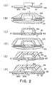
- a semiconductor deviceaccording to a first embodiment of this invention will be described in the order of manufacturing processes.
- a semiconductor element or chip 11is at first prepared which has a principal element surface directed downwards of Fig. 2(A), a bottom element surface directed upwards, and a plurality of bumps 11 a on the principal element surface.
- Each of the bumps 11 ais composed of Au in the illustrated example.
- a chip carrier 12is also prepared which comprises a resin or plastic substrate 121 of, for example, polyimide, epoxy.
- the resin substrate 121has a die attach surface and a package mounting surface which will be called a back surface and a front surface directed upwards and downwards of Fig. 2, respectively.
- the back and the front surfacesmay be referred to as upper and lower surfaces, respectively.
- a device holeis defined so as to mount the semiconductor element 11 within the device hole in a manner to be described later, as illustrated in Fig. 2 (A).
- the chip carrier 11comprises a plurality of leads 122 of copper which are attached to the resin substrate 121 and each of which is divided into an directed upwards and downwards of Fig. 1, respectively.
- a plurality of conductive leads (will be simply called leads hereinafter) 122are located or arranged on both the die attach surface and the package mounting surface of the resin substrate 121.
- Each of the leads 122is formed by a copper foil.
- Some of the leads 122 on the die attach surfaceare electrically connected to the other leads 122 on the package mounting surface through via holes 123.
- an electrodeis also placed on the die attach surface to support the semiconductor element 11.
- a plurality of solder balls or bumps 125 which serve as external terminalsare formed on the leads 122 attached to the package mounting surface of the resin substrate 121 and are surrounded by a solder mask which serves to define locations of the solder balls 125.
- the semiconductor element 11rests on the electrode formed on the die attach surface of the resin substrate 121 and the pads of the semiconductor element 11 are electrically connected through bonding wires 13 of Au to the leads 122 formed on the die attach surface. As a result, the pads of the semiconductor elements 11 are electrically connected to the solder balls 125.
- the semiconductor element 11is molded by the use of a resin material 15 which is formed on a side of the die attach surface and which will be called a resin mold hereinunder.
- the resin mold 15is attached only to the die attach surface inner lead 122a extended inwards of the device hole and an outer lead 122b placed outside of the inner lead 122a.
- Each outer lead 122bis supported on the upper surface of the resin substrate 122.
- a solder mask 14is formed on the lower surface of each outer lead 122b, as shown in Fig. 2(A).
- the solder mask 14has a plurality of holes for solder balls or bumps (will be described later). Thereafter, a mass of metal, such as Sn or Au, is plated on each inner lead 122a and in each hole. As a result, land portions for the solder balls are provided by plated portions in the holes.
- the chip carrier 12is completed in the above-mentioned manner.
- the semiconductor element 11is bonded to the inner leads 122a by the use of bumps 11 a on the upper surface of the resin substrate 121.
- the semiconductor element 11may be bonded to the inner leads 122a by a face down bonding technique, namely, a gang bonding method.
- a face down bonding techniquenamely, a gang bonding method.
- adoptation of the gang bonding methodmakes it possible to shorten a bonding time. Such an effect of shortening the bonding time becomes distinct as the number of the bumps 11 a is increased.
- Fig. 2(B)the semiconductor element 11 and the chip carrier 12 mentioned above are introduced into a mold which is composed of a first lower mold 101 and a first upper mold 102 and which is included in a transfer mold apparatus.
- the first lower mold 101has a center portion and a peripheral portion which surrounds the center portion.
- the center portionis recessed downwards of Fig. 2(B) relative to the peripheral portion while the peripheral portion is flat and is brought into contact with each outer lead 122b, as illustrated in Fig. 2-(B).
- the first upper mold 102has a peripheral region attached to the each outer lead 122b of the chip carrier 12 and a center region elevated from the peripheral region.
- the center portion of the first lower mold 101 and the center region of the first upper mold 102define an inner space or a cavity for accommodating the semiconductor element 11 and a part of the chip carrier 12.
- the outer leads 122bare cramped by the first upper and the first lower molds 102 and 101 with the semiconductor element 11 and the inner leads 122a enveloped within the cavity between the first upper and the first lower molds 102 and 101.
- a first molding processis conducted by causing molten resin to flow within the cavity.
- an epoxy resinwhich is a kind of cresol novolak resins is used while a phenol novolak resin is used as a hardening agent.
- silicais used as a filler to improve a thermal radiation characteristic.
- a provisional semiconductor device as shown in Fig. 2(C)is taken out of the transfer mold apparatus.
- a provisional semiconductor device as shown in Fig. 2(C)is taken out of the transfer mold apparatus.
- the first mold resin portion 15acovers not only the semiconductor element 11 but also a lower surface of each inner lead 122a together with a lower surface of a part of each outer lead 122b without any fins. This is because the first upper and the first lower molds 102 and 101 are closely attached to the chip carrier 12 without any gap. Thus, the first mold resin portion 15a envelopes the chip carrier 12 on both sides of the back and the front surfaces. In this event, the first mold resin portion 15a on the first surface of the chip carrier 12 may be called a first part while the first mold resin portion 15a on the back surface, a second part.
- the provisional semiconductor deviceis introduced into a second mold device which is composed of a second lower mold 103 and a second upper mold 104 and which is included in another transfer mold apparatus.
- the second lower mold 103has a center portion recessed relative to a peripheral portion and is attached to the chip carrier 12 and the first mold resin portion 15a on both lower sides of the chip carrier 12 and the first mold resin portion 15a.
- the second upper mold 104has an inside cavity defined by a peripheral contact surface, an inside side wall contiguous to the peripheral contact surface, and an inside center surface contiguous to the inside side surface.
- the peripheral contact surfaceis brought into contact with the upper surface of the chip carrier 12.
- the provisional semiconductor deviceis introduced and is located, as illustrated in Fig. 2(D). Thereafter, the second lower mold 103 and the second upper mold 104 are closed to cramp a peripheral portion of the chip carrier 12. In this situation, a lower surface of the first mold resin portion 15a and a lower surface of the chip carrier 12 are contacted with the second lower mold 103 while the upper surface of the peripheral portion of the chip carrier 12 is contacted with the second upper mold 104.
- molten resinis caused to flow within the inside cavity to carry out a second molding process so as to seal the provisional semiconductor device by the resin and to form a second mold resin portion 15b.
- the resinis identical with that used in the first molding process.
- a molded semiconductor deviceis taken out of the transfer mold apparatus and is sealed by the first and the second mold resin portions 15a and 15b, as shown in Fig. 2(E).
- the semiconductor deviceis heated for several hours to cure the first and the second mold resin portions 15a and 15b.
- solder balls 16are formed on the land portions deposited on the outer leads 122b, as illustrated in Fig. 2(F).
- solder ballscan be formed by soldering solder balls, by dripping molten solder by a disposer, or the like.
- the solder ballsmay be, for example, of an eutectic alloy of Pb and Sn.
- first and the second mold resin portions 15a and 15bare same resins used for the first and the second mold resin portions 15a and 15b in the above-mentioned example, different resins may be used to form the first and the second mold portions 15a and 15b. In the latter case, it is necessary to select the resins which have thermal expansion coefficients similar to each other.
- the inner leads 122aare completely enveloped by the first mold resin portion 15a.
- an upper part of the first mold resin portion 15ais covered with the second mold resin portion 15b.
- the illustrated semiconductor devicecan be remarkably improved in moisture proof.
- the first mold resin portion 15acan not be easily peeled from the chip carrier 12 because both upper and lower surfaces of the inner leads 122a are completely covered with the first mold resin portion 15a.
- a problem of peeling the first mold resin portion 15a from the inner leads 122a of the chip carrier 12can be avoided or solved by improving the moisture proof of the chip carrier 11.
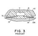
- the lower mold 109is brought into contact with the chip carrier at positions which are different from those of the upper mold 110 and that the lower mold 109 has a center portion recessed relative to a peripheral portion to form a cavity between the lower and the upper molds 109 and 110.
- the molten resinis caused to flow into the gap between the the chip carrier 12 and the lower mold 109, as depicted at 15'.
- the resultant molten resinremains as resin fins on a resin mold portion 15.
- the first lower mold 101 and the first upper mold 102 illustrated in Fig. 2(B)are brought into contact with the chip carrier 12 at positions which are substantially opposed to each other. Accordingly, it is possible to avoid occurrence of the fins on the lower part of the first mold resin portion 15a, as shown in Fig. 2(C). Thereafter, the second mold resin portion 15b is formed on the upper part of the first mold resin portion 15a by the second molding process.
- first and the second molding processesserve to avoid occurrence of the fins and to prevent the first and the second mold resin portions 15a and 15b from being peeled from the chip carrier 12.
- a semiconductor deviceaccording to a second embodiment of this invention will be described in the order of manufacturing processes and comprises similar parts designated by like reference numerals.
- the semiconductor element 11 and the chip carrier 12are prepared like in Fig. 2(A).
- the illustrated semiconductor element 11has front and back surfaces directed upwards and downwards of Fig. 4(A), respectively, and opposed to each other.
- the front surface of the semiconductor element 11may be referred to as a principal element surface like in Fig. 2 while the back surface may be called a back element surface.
- a plurality of bumps 11 aare formed on the principal element surface of the semiconductor element 11.
- the chip carrier 12includes the resin substrate 121 and the leads 122 of copper which are attached to the resin substrate 121 and which are divisible into inner leads 122a and outer leads 122b, like in Fig. 2.
- the inner leads 122aare extended inwards of the device hole of the resin substrate 121 while the outer leads 122b are coated with the solder mask 14 with the lands left therein.
- a lower surface of the resin substrate 121is also coated with a solder mask 14a which is effective to absorb stress imposed on a boundary face, as will become clear later.
- a heat spreader 20is mounted on the back element surface of the semiconductor element 11 to spread or radiate heat from the semiconductor element 11 into an atmosphere.
- the illustrated heat spreader 20has an upward surface, a downward surface opposite to the upward surface, and a side surface contiguous to the upward and the downward surfaces.
- the upward surface of the heat spreader 20is attached onto the back element surface of the semiconductor element 11 by the use of silver paste which forms a silver paste layer 21.
- the side surface of the heat spreader 20is projected outwards to form a projected portion 201.
- the bumps 11 a of the semiconductor element 11are at first bonded onto the inner leads 122. Subsequently, the silver paste is coated on the upward surface of the heat spreader 20 to form the silver paste layer 21. Under the circumstances, the chip carrier 12 is reversed or upset with the semiconductor element 11 attached to the chip carrier 12. As a result, the chip carrier 12 and the semiconductor element 11 are put into a state as shown in Fig. 4-(A). In this state, the semiconductor element 11 is located on the silver paste layer 21 coated on the heat spreader 20 and the silver paste is cured to attach the semiconductor element 21 to the heat spreader 20. Thus, an element unit illustrated in Fig. 4(A) is obtained which comprises the chip carrier 12, the semiconductor element 11, and the heat spreader 20.
- the element unitis introduced within a transfer mold apparatus which comprises a first lower mold (depicted at 105 in Fig. 4(B)) and a first upper mold (depicted at 106 in Fig. 4(B)).
- the first lower mold 105has a peripheral portion and a center portion which is recessed relative to the peripheral portion and which defines an inner space for accommodating the semiconductor element 11 and the heat spreader 20.
- the peripheral portion of the first lower mold 105substantially supports the outer leads 122b through the resin substrate 121 and the solder mask 14a.
- the first upper mold 106has a peripheral region confronted with the peripheral portion of the first lower portion 105 and a center region elevated from the peripheral region of the first upper mold 106.
- the first upper mold 106is brought into contact with the solder mask 14 at an area which is substantially opposed to that of the first lower mold 105, when the first upper mold 106 and the first lower mold 105 are closed.
- the first lower mold 105 and the first upper mold 106define an inner cavity which surrounds the inner leads 122a on both sides thereof.
- the outer leads 122bare cramped by the first lower mold 105 and the first upper mold 106.
- the downward surface of the heat spreader 20is contacted with the center portion of the first lower mold 105.
- molten resinis caused to flow into the inner cavity to carry out a first mold process of the semiconductor element 11.
- a molded element illustrated in Fig. 4-(C)is taken out of the transfer mold apparatus.
- the molded elementhas a first mold resin portion 15a which covers side surfaces of the semiconductor element 11 and the heat spreader 20 with the downward surface of the heat spreader 20 exposed to the atmosphere.
- the first mold resin portion 15acovers both upper and lower sides of the inner leads 122a without any fins. This is because the opposite regions of the outer leads 122b are cramped by the first lower mold 105 and the first upper mold 106, as illustrated in Fig. 4(B).
- the molded elementis located within another transfer mold apparatus that comprises a second lower mold (depicted at 107 in Fig. 4(D)) and a second upper mold (depicted at 108).
- the second upper mold 108has a center area contacted with an upper area of the first mold resin portion 15a and a peripheral area which can support the outer leads 122b. To this end, the center area of the second upper mold 108 is elevated relative to the peripheral area of the second upper mold 108.
- the second lower mold 107defines an inner lower space for accommodating the semiconductor element 11 and the heat spreader 20 and can support an outer peripheral portion of the chip carrier 12 and the heat spreader 20.
- the inner lower space defined by the second lower mold 107has a depth substantially equal to a height of the semiconductor element 11 and the heat spreader 20.
- the second lower mold 107 and the second upper mold 108are closed to cramp the molded element, the second lower mold 107 is attached to the outer peripheral portion of the chip carrier 12 and the downward surface of the heat spreader 20 while the second upper mold 108 is attached to the upper area of the first resin mold portion 15a and the chip carrier 12 on the outer leads 122b.
- a second mold processis carried out by causing molten resin to flow into the inner cavity defined by the second lower mold 107 and the second upper mold 108.
- a provisional semiconductor deviceis taken out of the transfer mold apparatus and comprises a second resin mold portion 15b covered on the first resin mold portion 15a.
- the provisional semiconductor deviceis sealed in double by the first and the second resin mold portions 15a and 15b.
- the semiconductor device illustrated in Fig. 4(E)is obtained by forming a plurality of solder balls 16 on the outer leads 122b.
- the heat spreader 20has the downward surface which is directed upwards of Fig. 4(E) and which is exposed to the atmosphere. Accordingly, heat from the semiconductor element 11 can be effectively radiated from the heat spreader 20.
- solder mask 14ais attached to the first and the second resin mold portions 15a and 15b in the illustrated example.
- the solder mask 14aserves to absorb stress imposed on the boundary face between the chip carrier 12 and each of the first and the second resin mold portions 15a and 15b and to improve adhesion between the resin substrate 121 and each of the first and the second resin mold portions 15a and 15b.
- the projected portion 201is formed on the side surface of the heat spreader 20 and lends itself not only to strongly couple the first resin mold portion 15a to the heat spreader 20 but also to prevent invasion of moisture which passes through a boundary face between the first resin mold portion 15a and the heat spreader 20. Such prevention of invasion of moisture can be accomplished by lengthening an invasion path by forming the projected portion 201. Therefore, a plurality of projected portions may be formed on the side surface of the heat spreader 20.
- the heat spreader 20may be buried within a resin mold portion.
- a semiconductor deviceis similar in structure to that illustrated in Fig. 2 except that leads 122 and 122a are formed on both surfaces of the resin substrate 121, as shown in Fig. 5.
- the leads 122 on one surface of the resin substrate 121are electrically connected to the leads 122a on another surface of the resin substrate 121 through via holes 123.
- the illustrated chip carrier 12has a plurality of lead layers composed of the leads 122 and 122a and enables high density wiring. In addition, it is possible to increase a degree of freedom in relation to the wiring.
- solder balls 16may be replaced by metallic balls, such as copper balls.
- the bumps 11 a of the semiconductor element 11may be formed by solder bumps.
- the semiconductor element 11may have no bump and, instead, aluminum pads formed on the semiconductor element.
- the aluminum padsare directly connected to the leads of copper by a tape automated bonding (TAB) technique.
- TABtape automated bonding
- studs of copperare deposited on the inner leads of the chip carrier 12. At any rate, connections are made by an alloy of aluminum and copper.
- the semiconductor element 11may be coated with a bonding resin layer before the first mold process is carried out.
Landscapes
- Engineering & Computer Science (AREA)
- Microelectronics & Electronic Packaging (AREA)
- Physics & Mathematics (AREA)
- Condensed Matter Physics & Semiconductors (AREA)
- General Physics & Mathematics (AREA)
- Computer Hardware Design (AREA)
- Power Engineering (AREA)
- Manufacturing & Machinery (AREA)
- Structures Or Materials For Encapsulating Or Coating Semiconductor Devices Or Solid State Devices (AREA)
- Encapsulation Of And Coatings For Semiconductor Or Solid State Devices (AREA)
Abstract
Description
- This invention relates to a semiconductor device which has a semiconductor element sealed by a synthetic resin (will be simply called a resin hereinunder) and mounted on a chip carrier, such as a tape carrier.
- As a rule, it is a recent trend that a semiconductor device becomes small in size, thin in thickness, and light in weight. In order to be matched with this trend, automation has been made also as regards an assembling process of mounting a semiconductor element or chip onto a package which has a plurality of wiring patterns or outer leads on a package surface. Since the semiconductor element is mounted or attached onto the package surface of the package, the above-mentioned assembling process is referred to as a surface mounting method in the art. The surface mounting method has been usually adopted in a semiconductor device of a Quad Flat Package (QFP) structure or a Small Outline J-Ieaded Package (SOJ) structure.
- Herein, it is to be noted that the outer leads are located along an outer periphery of the package and are one-dimensionally extended and that they are electrically connected to electrodes of the semiconductor elements by the use of conductive wires one by one.
- With this structure, a spacing or a pitch between two adjacent ones of the electrodes of the semiconductor element becomes narrow as the electrodes are increased in number. Such a narrow pitch makes a mounting process difficult when the pitch becomes narrow over a limit of a mounting technique.
- On the other hand, a semiconductor device has been proposed in United States Patent No. 5,216,278 issued to Paul T. Lin et al and has a package structure known as a Ball Grid Array (BGA). With this structure, it is possible to derive wiring patterns two-dimensionally from the electrodes of the semiconductor element arranged two-dimensionally in the form of pads on the semiconductor element.
- More specifically, the package structure comprises a carrier substrate of a flexible material, such as a resin material, which has a die attach surface and a package mounting surface opposite to the die attach surface. A semiconductor element which has a plurality of pads is bonded to the die attach surface through a conductive layer. Any other package leads are arranged around the semiconductor element on the die attach surface and are electrically connected to the pads on the semiconductor element through conductive lines. Some of the package leads are electrically connected through via holes to package leads formed on the package mounting surface.
- A plurality of solder balls are placed on the package leads on the package mounting surface to be attached to a printed circuit board. Thus, a combination of the carrier substrate and the package leads on the die attach surface and the package mounting surface may be collectively called a chip carrier.
- Furthermore, the semiconductor element on the die attach surface of the carrier substrate is sealed or molded by a resin material.
- With this structure, the resin material is formed only on a side of the die attach surface of the carrier substrate. This shows that the resin material is adhered to the chip carrier only on a side of the die attach surface with a side of the package mounting surface uncovered with the resin material.
- Consequently, the resin material is fixed to the chip carrier only by adhesion of the resin material.
- Herein, it is to be noted that the resin material is liable to absorb moisture and has a thermal expansion coefficient different from that of the chip carrier. In addition, the carrier substrate itself has a high hygroscopicity.
- Moreover, such a semiconductor device of the type described is heated on mounting the semiconductor device onto the printed circuit board so as to melt the solder balls and to attach the semiconductor device to electrodes laid on the printed circuit board.
- Under the circumstances, the semiconductor device is disadvantageous in that the resin material is easily peeled from the chip carrier when the semiconductor device is heated on mounting the semiconductor device onto the printed circuit board. This is because evaporation of moisture takes place in the resin material by a heat treatment on mounting the semiconductor device onto the printed circuit board and the resin material is largely expanded in comparison with the chip carrier.
- Taking the above into consideration, the resin material is dried within an oven to eliminate the moisture before the semiconductor device is mounted onto the printed circuit board. Thus, the semiconductor device should be deliberately handled in order to prevent the resin material from being peeled from the chip carrier. As a result, the semiconductor device is troublesome in handling.
- Furthermore, the semiconductor device is degraded in characteristics and can not be guaranteed in a long term reliability because the semiconductor device is directly bonded on the chip carrier which has a high hygroscopicity and is also not sealed by a resin material.
- In addition, since the conductive lines are used to electrically connect the pads of the semiconductor element to the leads, a pitch between two adjacent ones of the pads should be equal to or wider than 120 micron meters. As a result, it is difficult with the above-mentioned method to mount, on the chip carrier, a semiconductor element which has a pitch narrower than 120 micron meters.
- The semiconductor device also has disadvantages that bonding strength of connections is weak between the leads and the conductive lines, because the leads are formed by copper which is soft and which can not be heated to a high temperature.
- Moreover, long electrical paths are required between the pads of the semiconductor element and the printed circuit board, which results in a long transmission delay time and a large noise.
- It is an object of this invention to provide a semiconductor device which is capable of removing disadvantages enumerated above.
- It is a specific object of this invention to provide a semiconductor device of the type described, which can prevent a resin material from being peeled from a chip carrier.
- It is another object of this invention to provide a semiconductor of the type described, which can guarantee a long term reliability.
- It is still another object of this invention to provide a semiconductor of the type described, which can reduce noise and shorten a transmission delay time.
- According to an aspect of this invention, a semiconductor device comprises a chip carrier which has a front surface and a back surface opposite to the front surface and which is formed by a resin substrate and a plurality of leads attached to the resin substrate on the front surface, a semiconductor element having a principal element surface electrically connected to the leads and a bottom element surface opposite to the principal element surface, a first mold resin portion which covers the semiconductor element on both sides of the front and the back surfaces of the chip carrier together with a part of the leads adjacent to the semiconductor element to seal the semiconductor element within the first mold resin portion, and a second mold resin portion which covers the first mold resin portion on a side of the back surface of the chip carrier.
- According to another aspect of this invention, a method is for use in manufacturing a semiconductor device which comprises a chip carrier and a semiconductor element mounted on the chip carrier. The method comprises the steps of sealing the semiconductor element by a mold resin to form a first mold resin portion and sealing a part of the first resin portion by another mold resin to form a second mold resin portion and to obtain the semiconductor device.
- Fig. 1 is a sectional view of a conventional semiconductor device;
- Figs. 2(A) to 2(F) are sectional views for use in describing processes of manufacturing a semiconductor device according to a first embodiment of this invention in order;
- Fig. 3 is a sectional view for use in describing defects which occur in the conventional semiconductor device;
- Figs. 4(A) to 4(E) are sectional views for use in describing processes of manufacturing a semiconductor device according to a second embodiment of this invention; and
- Fig. 5 is a sectional view of a semiconductor device according to a third embodiment of this invention.
- Referring to Fig. 1, description will be at first made about a conventional semiconductor device which is substantially equivalent to that described in U.S. Patent No. 5,216,278 referenced in the preamble of the instant specification. The conventional semiconductor device has been called a ball grid array semiconductor device of a plastic or resin seal type and comprises a semiconductor element or
chip 11 and achip carrier 12. - The
semiconductor element 11 has an upper element surface, a lower element surface, and a plurality of pads which serve as electrodes and which are formed on the upper surface of thesemiconductor element 11, as shown in Fig. 1. The upper element surface may be called a principal element surface while the lower element surface may be called a bottom element surface. - The
chip carrier 12 comprises a plastic orresin substrate 121 of, for example, a glass epoxy resin material having a die attach surface and a package mounting surface side alone and that the pads of the semiconductor device are directed upwards of Fig. 1. Therefore, the illustrated semiconductor device has shortcomings as pointed out in the preamble of the instant specification. - Referring to Figs. 2(A) to (F), a semiconductor device according to a first embodiment of this invention will be described in the order of manufacturing processes. In Fig. 2(A), a semiconductor element or
chip 11 is at first prepared which has a principal element surface directed downwards of Fig. 2(A), a bottom element surface directed upwards, and a plurality of bumps 11 a on the principal element surface. Each of the bumps 11 a is composed of Au in the illustrated example. - On the other hand, a
chip carrier 12 is also prepared which comprises a resin orplastic substrate 121 of, for example, polyimide, epoxy. Theresin substrate 121 has a die attach surface and a package mounting surface which will be called a back surface and a front surface directed upwards and downwards of Fig. 2, respectively. In this connection, the back and the front surfaces may be referred to as upper and lower surfaces, respectively. - Inside the
resin substrate 121, a device hole is defined so as to mount thesemiconductor element 11 within the device hole in a manner to be described later, as illustrated in Fig. 2 (A). - In addition, the
chip carrier 11 comprises a plurality ofleads 122 of copper which are attached to theresin substrate 121 and each of which is divided into an directed upwards and downwards of Fig. 1, respectively. A plurality of conductive leads (will be simply called leads hereinafter) 122 are located or arranged on both the die attach surface and the package mounting surface of theresin substrate 121. Each of theleads 122 is formed by a copper foil. Some of theleads 122 on the die attach surface are electrically connected to the other leads 122 on the package mounting surface through via holes 123. In addition, an electrode is also placed on the die attach surface to support thesemiconductor element 11. - A plurality of solder balls or bumps 125 which serve as external terminals are formed on the
leads 122 attached to the package mounting surface of theresin substrate 121 and are surrounded by a solder mask which serves to define locations of the solder balls 125. - As shown in Fig. 1, the
semiconductor element 11 rests on the electrode formed on the die attach surface of theresin substrate 121 and the pads of thesemiconductor element 11 are electrically connected throughbonding wires 13 of Au to theleads 122 formed on the die attach surface. As a result, the pads of thesemiconductor elements 11 are electrically connected to the solder balls 125. - The
semiconductor element 11 is molded by the use of aresin material 15 which is formed on a side of the die attach surface and which will be called a resin mold hereinunder. - From the above, it is readily understood that the
resin mold 15 is attached only to the die attach surfaceinner lead 122a extended inwards of the device hole and anouter lead 122b placed outside of theinner lead 122a. Eachouter lead 122b is supported on the upper surface of theresin substrate 122. Asolder mask 14 is formed on the lower surface of eachouter lead 122b, as shown in Fig. 2(A). Thesolder mask 14 has a plurality of holes for solder balls or bumps (will be described later). Thereafter, a mass of metal, such as Sn or Au, is plated on eachinner lead 122a and in each hole. As a result, land portions for the solder balls are provided by plated portions in the holes. At any rate, thechip carrier 12 is completed in the above-mentioned manner. - With this structure, the
semiconductor element 11 is bonded to theinner leads 122a by the use of bumps 11 a on the upper surface of theresin substrate 121. For example, thesemiconductor element 11 may be bonded to theinner leads 122a by a face down bonding technique, namely, a gang bonding method. Thus, adoptation of the gang bonding method makes it possible to shorten a bonding time. Such an effect of shortening the bonding time becomes distinct as the number of the bumps 11 a is increased. - In Fig. 2(B), the
semiconductor element 11 and thechip carrier 12 mentioned above are introduced into a mold which is composed of a first lower mold 101 and a firstupper mold 102 and which is included in a transfer mold apparatus. The first lower mold 101 has a center portion and a peripheral portion which surrounds the center portion. The center portion is recessed downwards of Fig. 2(B) relative to the peripheral portion while the peripheral portion is flat and is brought into contact with eachouter lead 122b, as illustrated in Fig. 2-(B). - On the other hand, the first
upper mold 102 has a peripheral region attached to the eachouter lead 122b of thechip carrier 12 and a center region elevated from the peripheral region. The center portion of the first lower mold 101 and the center region of the firstupper mold 102 define an inner space or a cavity for accommodating thesemiconductor element 11 and a part of thechip carrier 12. - Under the circumstances, the outer leads 122b are cramped by the first upper and the first
lower molds 102 and 101 with thesemiconductor element 11 and theinner leads 122a enveloped within the cavity between the first upper and the firstlower molds 102 and 101. In this situation, a first molding process is conducted by causing molten resin to flow within the cavity. As a molding or sealing resin, an epoxy resin which is a kind of cresol novolak resins is used while a phenol novolak resin is used as a hardening agent. In addition, silica is used as a filler to improve a thermal radiation characteristic. - After the resin is hardened, a provisional semiconductor device as shown in Fig. 2(C) is taken out of the transfer mold apparatus. Thus, it is possible to obtain the provisional provisional device sealed by a first
mold resin portion 15a. - Herein, it is to be noted that the first
mold resin portion 15a covers not only thesemiconductor element 11 but also a lower surface of eachinner lead 122a together with a lower surface of a part of eachouter lead 122b without any fins. This is because the first upper and the firstlower molds 102 and 101 are closely attached to thechip carrier 12 without any gap. Thus, the firstmold resin portion 15a envelopes thechip carrier 12 on both sides of the back and the front surfaces. In this event, the firstmold resin portion 15a on the first surface of thechip carrier 12 may be called a first part while the firstmold resin portion 15a on the back surface, a second part. - Thereafter, the provisional semiconductor device is introduced into a second mold device which is composed of a second
lower mold 103 and a secondupper mold 104 and which is included in another transfer mold apparatus. The secondlower mold 103 has a center portion recessed relative to a peripheral portion and is attached to thechip carrier 12 and the firstmold resin portion 15a on both lower sides of thechip carrier 12 and the firstmold resin portion 15a. - On the other hand, the second
upper mold 104 has an inside cavity defined by a peripheral contact surface, an inside side wall contiguous to the peripheral contact surface, and an inside center surface contiguous to the inside side surface. The peripheral contact surface is brought into contact with the upper surface of thechip carrier 12. - Within the inside cavity formed between the second
lower mold 103 and the secondupper mold 104, the provisional semiconductor device is introduced and is located, as illustrated in Fig. 2(D). Thereafter, the secondlower mold 103 and the secondupper mold 104 are closed to cramp a peripheral portion of thechip carrier 12. In this situation, a lower surface of the firstmold resin portion 15a and a lower surface of thechip carrier 12 are contacted with the secondlower mold 103 while the upper surface of the peripheral portion of thechip carrier 12 is contacted with the secondupper mold 104. - Subsequently, molten resin is caused to flow within the inside cavity to carry out a second molding process so as to seal the provisional semiconductor device by the resin and to form a second
mold resin portion 15b. The resin is identical with that used in the first molding process. - After the molten resin is hardened, a molded semiconductor device is taken out of the transfer mold apparatus and is sealed by the first and the second
mold resin portions - Furthermore, the semiconductor device is heated for several hours to cure the first and the second
mold resin portions - Thereafter,
solder balls 16 are formed on the land portions deposited on the outer leads 122b, as illustrated in Fig. 2(F). Such solder balls can be formed by soldering solder balls, by dripping molten solder by a disposer, or the like. The solder balls may be, for example, of an eutectic alloy of Pb and Sn. - Although the same resin is used for the first and the second
mold resin portions second mold portions - As illustrated in Fig. 2(F), the
inner leads 122a are completely enveloped by the firstmold resin portion 15a. In addition, an upper part of the firstmold resin portion 15a is covered with the secondmold resin portion 15b. - With this structure, it is possible to compensate for mechanical strength of the
chip carrier 12 and to assure flatness of the outer leads 122b because the secondmold resin portion 15b is formed onto the firstmold resin portion 15a. In this event, an upper surface of the firstmold resin portion 15a may not be always covered with the secondmold resin portion 15b. - More specifically, since the
semiconductor element 11 is completely enveloped by the firstmold resin portion 15a, the illustrated semiconductor device can be remarkably improved in moisture proof. The firstmold resin portion 15a can not be easily peeled from thechip carrier 12 because both upper and lower surfaces of theinner leads 122a are completely covered with the firstmold resin portion 15a. A problem of peeling the firstmold resin portion 15a from the inner leads 122a of thechip carrier 12 can be avoided or solved by improving the moisture proof of thechip carrier 11. - Practically, it has been found out in the semiconductor device illustrated in Fig. 2 that the first
mold resin portion 15a is not peeled from theinner leads 122a even when the semiconductor device illustrated in Fig. 2(F) is mounted on a print circuit board after lapse of seventy-two hours, although the conventional semiconductor device illustrated in Fig. 1 should be mounted within twenty-four hours after it is dried in an oven. - Herein, it is to be noted that none of fins take place on the first and the second
mold resin portions lower mold 103 and the second upper mold 104 (Fig. 2(D)) should be prepared, as illustrated in Fig. 3, and are depicted at 109 and 110 in Fig. 3. It should be noted that thelower mold 109 is brought into contact with the chip carrier at positions which are different from those of theupper mold 110 and that thelower mold 109 has a center portion recessed relative to a peripheral portion to form a cavity between the lower and theupper molds - Under the circumstances, when molten resin is introduced into the cavity between the lower and the
upper molds lower mold 109 and to somewhat push up thechip carrier 12 upwards of Fig. 3. As a result, thechip carrier 12 is partially detached from thelower mold 109 by the molten resin, which brings about occurrence of a gap between thechip carrier 12 and thelower mold 109. - Thus, the molten resin is caused to flow into the gap between the the
chip carrier 12 and thelower mold 109, as depicted at 15'. The resultant molten resin remains as resin fins on aresin mold portion 15. - On the other hand, when the first lower mold 101 and the first
upper mold 102 illustrated in Fig. 2(B) are brought into contact with thechip carrier 12 at positions which are substantially opposed to each other. Accordingly, it is possible to avoid occurrence of the fins on the lower part of the firstmold resin portion 15a, as shown in Fig. 2(C). Thereafter, the secondmold resin portion 15b is formed on the upper part of the firstmold resin portion 15a by the second molding process. - From this fact, it is readily understood that the first and the second molding processes serve to avoid occurrence of the fins and to prevent the first and the second
mold resin portions chip carrier 12. - Referring to Figs. 4(A) to 4(E), a semiconductor device according to a second embodiment of this invention will be described in the order of manufacturing processes and comprises similar parts designated by like reference numerals. In Fig. 4(A), the
semiconductor element 11 and thechip carrier 12 are prepared like in Fig. 2(A). Specifically, the illustratedsemiconductor element 11 has front and back surfaces directed upwards and downwards of Fig. 4(A), respectively, and opposed to each other. The front surface of thesemiconductor element 11 may be referred to as a principal element surface like in Fig. 2 while the back surface may be called a back element surface. A plurality of bumps 11 a are formed on the principal element surface of thesemiconductor element 11. - The
chip carrier 12 includes theresin substrate 121 and theleads 122 of copper which are attached to theresin substrate 121 and which are divisible intoinner leads 122a andouter leads 122b, like in Fig. 2. Theinner leads 122a are extended inwards of the device hole of theresin substrate 121 while the outer leads 122b are coated with thesolder mask 14 with the lands left therein. In the example being illustrated, a lower surface of theresin substrate 121 is also coated with asolder mask 14a which is effective to absorb stress imposed on a boundary face, as will become clear later. - Herein, it is noted that a
heat spreader 20 is mounted on the back element surface of thesemiconductor element 11 to spread or radiate heat from thesemiconductor element 11 into an atmosphere. The illustratedheat spreader 20 has an upward surface, a downward surface opposite to the upward surface, and a side surface contiguous to the upward and the downward surfaces. The upward surface of theheat spreader 20 is attached onto the back element surface of thesemiconductor element 11 by the use of silver paste which forms asilver paste layer 21. The side surface of theheat spreader 20 is projected outwards to form a projectedportion 201. - Now, description will be made about processes of manufacturing the semiconductor device. The bumps 11 a of the
semiconductor element 11 are at first bonded onto the inner leads 122. Subsequently, the silver paste is coated on the upward surface of theheat spreader 20 to form thesilver paste layer 21. Under the circumstances, thechip carrier 12 is reversed or upset with thesemiconductor element 11 attached to thechip carrier 12. As a result, thechip carrier 12 and thesemiconductor element 11 are put into a state as shown in Fig. 4-(A). In this state, thesemiconductor element 11 is located on thesilver paste layer 21 coated on theheat spreader 20 and the silver paste is cured to attach thesemiconductor element 21 to theheat spreader 20. Thus, an element unit illustrated in Fig. 4(A) is obtained which comprises thechip carrier 12, thesemiconductor element 11, and theheat spreader 20. - In Fig. 4(B), the element unit is introduced within a transfer mold apparatus which comprises a first lower mold (depicted at 105 in Fig. 4(B)) and a first upper mold (depicted at 106 in Fig. 4(B)). The first
lower mold 105 has a peripheral portion and a center portion which is recessed relative to the peripheral portion and which defines an inner space for accommodating thesemiconductor element 11 and theheat spreader 20. The peripheral portion of the firstlower mold 105 substantially supports the outer leads 122b through theresin substrate 121 and thesolder mask 14a. - On the other hand, the first
upper mold 106 has a peripheral region confronted with the peripheral portion of the firstlower portion 105 and a center region elevated from the peripheral region of the firstupper mold 106. - Thus, the first
upper mold 106 is brought into contact with thesolder mask 14 at an area which is substantially opposed to that of the firstlower mold 105, when the firstupper mold 106 and the firstlower mold 105 are closed. In addition, the firstlower mold 105 and the firstupper mold 106 define an inner cavity which surrounds theinner leads 122a on both sides thereof. - After the element unit is introduced within the inner cavity between the first
lower mold 105 and the firstupper mold 106, the outer leads 122b are cramped by the firstlower mold 105 and the firstupper mold 106. In the example being illustrated, the downward surface of theheat spreader 20 is contacted with the center portion of the firstlower mold 105. - Next, molten resin is caused to flow into the inner cavity to carry out a first mold process of the
semiconductor element 11. After the molten resin is hardened, a molded element illustrated in Fig. 4-(C) is taken out of the transfer mold apparatus. - As shown in Fig. 4(C), the molded element has a first
mold resin portion 15a which covers side surfaces of thesemiconductor element 11 and theheat spreader 20 with the downward surface of theheat spreader 20 exposed to the atmosphere. The firstmold resin portion 15a covers both upper and lower sides of theinner leads 122a without any fins. This is because the opposite regions of the outer leads 122b are cramped by the firstlower mold 105 and the firstupper mold 106, as illustrated in Fig. 4(B). - Subsequently, the molded element is located within another transfer mold apparatus that comprises a second lower mold (depicted at 107 in Fig. 4(D)) and a second upper mold (depicted at 108).
- As readily understood from Fig. 4(D), the second
upper mold 108 has a center area contacted with an upper area of the firstmold resin portion 15a and a peripheral area which can support the outer leads 122b. To this end, the center area of the secondupper mold 108 is elevated relative to the peripheral area of the secondupper mold 108. - On the other hand, the second
lower mold 107 defines an inner lower space for accommodating thesemiconductor element 11 and theheat spreader 20 and can support an outer peripheral portion of thechip carrier 12 and theheat spreader 20. Specifically, the inner lower space defined by the secondlower mold 107 has a depth substantially equal to a height of thesemiconductor element 11 and theheat spreader 20. - When the second
lower mold 107 and the secondupper mold 108 are closed to cramp the molded element, the secondlower mold 107 is attached to the outer peripheral portion of thechip carrier 12 and the downward surface of theheat spreader 20 while the secondupper mold 108 is attached to the upper area of the firstresin mold portion 15a and thechip carrier 12 on the outer leads 122b. - Under the circumstances, a second mold process is carried out by causing molten resin to flow into the inner cavity defined by the second
lower mold 107 and the secondupper mold 108. After the molten resin is hardened, a provisional semiconductor device is taken out of the transfer mold apparatus and comprises a secondresin mold portion 15b covered on the firstresin mold portion 15a. Thus, the provisional semiconductor device is sealed in double by the first and the secondresin mold portions - After the provisional semiconductor device is heated for several hours to cure the first and the second
resin mold portions solder balls 16 on the outer leads 122b. - Herein, it is to be noted that the
heat spreader 20 has the downward surface which is directed upwards of Fig. 4(E) and which is exposed to the atmosphere. Accordingly, heat from thesemiconductor element 11 can be effectively radiated from theheat spreader 20. - In addition, the
solder mask 14a is attached to the first and the secondresin mold portions solder mask 14a serves to absorb stress imposed on the boundary face between thechip carrier 12 and each of the first and the secondresin mold portions resin substrate 121 and each of the first and the secondresin mold portions - Moreover, since the projected
portion 201 is formed on the side surface of theheat spreader 20 and lends itself not only to strongly couple the firstresin mold portion 15a to theheat spreader 20 but also to prevent invasion of moisture which passes through a boundary face between the firstresin mold portion 15a and theheat spreader 20. Such prevention of invasion of moisture can be accomplished by lengthening an invasion path by forming the projectedportion 201. Therefore, a plurality of projected portions may be formed on the side surface of theheat spreader 20. - If an excellent moisture proof is required for the semiconductor device, the
heat spreader 20 may be buried within a resin mold portion. - Referring to Fig. 5, a semiconductor device according to a third embodiment of this invention is similar in structure to that illustrated in Fig. 2 except that leads 122 and 122a are formed on both surfaces of the
resin substrate 121, as shown in Fig. 5. The leads 122 on one surface of theresin substrate 121 are electrically connected to theleads 122a on another surface of theresin substrate 121 through viaholes 123. - Thus, the illustrated
chip carrier 12 has a plurality of lead layers composed of theleads - While this invention has thus far been described in conjunction with a few embodiments thereof, it will readily be possible for those skilled in the art to put this invention into practice in various other manners. For example, the
solder balls 16 may be replaced by metallic balls, such as copper balls. The bumps 11 a of thesemiconductor element 11 may be formed by solder bumps. Moreover, thesemiconductor element 11 may have no bump and, instead, aluminum pads formed on the semiconductor element. In this event, the aluminum pads are directly connected to the leads of copper by a tape automated bonding (TAB) technique. It is preferable that studs of copper are deposited on the inner leads of thechip carrier 12. At any rate, connections are made by an alloy of aluminum and copper. - Furthermore, the
semiconductor element 11 may be coated with a bonding resin layer before the first mold process is carried out.
Claims (14)
said balls being higher than said first part.
said second mold resin portion sealing the first mold resin portion on the side of the back surface.
Applications Claiming Priority (3)
| Application Number | Priority Date | Filing Date | Title |
|---|---|---|---|
| JP6134885AJP2531382B2 (en) | 1994-05-26 | 1994-05-26 | Ball grid array semiconductor device and manufacturing method thereof |
| JP134885/94 | 1994-05-26 | ||
| JP13488594 | 1994-05-26 |
Publications (3)
| Publication Number | Publication Date |
|---|---|
| EP0684641A2true EP0684641A2 (en) | 1995-11-29 |
| EP0684641A3 EP0684641A3 (en) | 1996-11-06 |
| EP0684641B1 EP0684641B1 (en) | 2003-02-26 |
Family
ID=15138791
Family Applications (1)
| Application Number | Title | Priority Date | Filing Date |
|---|---|---|---|
| EP95107867AExpired - LifetimeEP0684641B1 (en) | 1994-05-26 | 1995-05-23 | Semiconductor device moulding capable of accomplishing a high moisture proof |
Country Status (5)
| Country | Link |
|---|---|
| US (2) | US5989940A (en) |
| EP (1) | EP0684641B1 (en) |
| JP (1) | JP2531382B2 (en) |
| KR (1) | KR0152700B1 (en) |
| DE (1) | DE69529698T2 (en) |
Cited By (8)
| Publication number | Priority date | Publication date | Assignee | Title |
|---|---|---|---|---|
| EP0915505A1 (en)* | 1997-11-06 | 1999-05-12 | Sharp Kabushiki Kaisha | Semiconductor device package, manufacturing method thereof and circuit board therefor |
| WO1999016132A3 (en)* | 1997-09-22 | 1999-06-17 | Siemens Ag | Method for producing a plastic composite body and plastic composite body |
| FR2805392A1 (en)* | 2000-02-17 | 2001-08-24 | Bull Sa | OVER-INTEGRATED CIRCUIT BOX |
| EP1189271A3 (en)* | 1996-07-12 | 2003-07-16 | Fujitsu Limited | Wiring boards and mounting of semiconductor devices thereon |
| US6881611B1 (en) | 1996-07-12 | 2005-04-19 | Fujitsu Limited | Method and mold for manufacturing semiconductor device, semiconductor device and method for mounting the device |
| WO2010091967A1 (en)* | 2009-02-12 | 2010-08-19 | Osram Opto Semiconductors Gmbh | Encapsulated opto-electronic semiconductor arrangement having solder stop layer and corresponding method |
| CN106206469A (en)* | 2015-05-29 | 2016-12-07 | 爱思开海力士有限公司 | Semiconductor packages and manufacture method thereof |
| CN107275236A (en)* | 2016-04-05 | 2017-10-20 | 东和株式会社 | resin encapsulation equipment and resin encapsulation method |
Families Citing this family (66)
| Publication number | Priority date | Publication date | Assignee | Title |
|---|---|---|---|---|
| JP3007497B2 (en)* | 1992-11-11 | 2000-02-07 | 三菱電機株式会社 | Semiconductor integrated circuit device, its manufacturing method, and its mounting method |
| JP2531382B2 (en)* | 1994-05-26 | 1996-09-04 | 日本電気株式会社 | Ball grid array semiconductor device and manufacturing method thereof |
| USRE39426E1 (en) | 1996-06-19 | 2006-12-12 | International Business Machines Corporation | Thermally enhanced flip chip package and method of forming |
| EP0886313A4 (en)* | 1996-12-04 | 2001-02-28 | Shinko Electric Ind Co | Semiconductor device sealed with resin, and its manufacture |
| JP3671563B2 (en)* | 1996-12-09 | 2005-07-13 | 株式会社デンソー | Semiconductor device having a structure in which a mold IC is fixed to a case |
| JP3032964B2 (en)* | 1996-12-30 | 2000-04-17 | アナムインダストリアル株式会社 | Ball grid array semiconductor package and manufacturing method |
| JP3398004B2 (en)* | 1997-03-24 | 2003-04-21 | ローム株式会社 | Package type semiconductor device structure |
| JPH10294418A (en)* | 1997-04-21 | 1998-11-04 | Oki Electric Ind Co Ltd | Semiconductor device |
| JPH10321631A (en)* | 1997-05-19 | 1998-12-04 | Oki Electric Ind Co Ltd | Semiconductor device and its manufacture |
| KR19990005515A (en)* | 1997-06-30 | 1999-01-25 | 윤종용 | Manufacturing Method of COB Package Using Mold |
| KR100246366B1 (en)* | 1997-12-04 | 2000-03-15 | 김영환 | Area array type semiconductor package and fabrication method of the same |
| JP3087709B2 (en)* | 1997-12-08 | 2000-09-11 | 日本電気株式会社 | Semiconductor device and manufacturing method thereof |
| JPH11260863A (en)* | 1998-03-09 | 1999-09-24 | Sumitomo Electric Ind Ltd | Connection terminal for semiconductor device and manufacturing method thereof |
| TW469611B (en)* | 1998-03-12 | 2001-12-21 | Delta Electronics Inc | Packaging method for electronic device |
| JPH11283593A (en)* | 1998-03-27 | 1999-10-15 | Mitsumi Electric Co Ltd | Battery pack |
| JP3648053B2 (en) | 1998-04-30 | 2005-05-18 | 沖電気工業株式会社 | Semiconductor device |
| US6329709B1 (en)* | 1998-05-11 | 2001-12-11 | Micron Technology, Inc. | Interconnections for a semiconductor device |
| US6190945B1 (en)* | 1998-05-21 | 2001-02-20 | Micron Technology, Inc. | Integrated heat sink |
| KR100266693B1 (en) | 1998-05-30 | 2000-09-15 | 김영환 | Stackable ball grid array semiconductor package and fabrication method thereof |
| KR100266698B1 (en)* | 1998-06-12 | 2000-09-15 | 김영환 | Semiconductor chip package and fabrication method thereof |
| JP2000068436A (en)* | 1998-08-18 | 2000-03-03 | Oki Electric Ind Co Ltd | Semiconductor device and frame for the semiconductor device |
| US6515355B1 (en)* | 1998-09-02 | 2003-02-04 | Micron Technology, Inc. | Passivation layer for packaged integrated circuits |
| US6008074A (en)* | 1998-10-01 | 1999-12-28 | Micron Technology, Inc. | Method of forming a synchronous-link dynamic random access memory edge-mounted device |
| AU779395B2 (en)* | 1999-04-30 | 2005-01-20 | Institut De Recherche Cliniques De Montreal (Ircm) | Mutant human CD80 and compositions for and methods of making and using the same |
| US6274397B1 (en)* | 1999-06-01 | 2001-08-14 | Taiwan Semiconductor Manufacturing Company Ltd. | Method to preserve the testing chip for package's quality |
| JP3277996B2 (en)* | 1999-06-07 | 2002-04-22 | 日本電気株式会社 | Circuit device and method of manufacturing the same |
| US6122171A (en)* | 1999-07-30 | 2000-09-19 | Micron Technology, Inc. | Heat sink chip package and method of making |
| US6700210B1 (en) | 1999-12-06 | 2004-03-02 | Micron Technology, Inc. | Electronic assemblies containing bow resistant semiconductor packages |
| US6384487B1 (en)* | 1999-12-06 | 2002-05-07 | Micron Technology, Inc. | Bow resistant plastic semiconductor package and method of fabrication |
| JP2002009097A (en)* | 2000-06-22 | 2002-01-11 | Oki Electric Ind Co Ltd | Semiconductor device and method of manufacturing the same |
| US6818968B1 (en)* | 2000-10-12 | 2004-11-16 | Altera Corporation | Integrated circuit package and process for forming the same |
| US6645794B2 (en) | 2000-10-18 | 2003-11-11 | Hitachi, Ltd. | Method of manufacturing a semiconductor device by monolithically forming a sealing resin for sealing a chip and a reinforcing frame by transfer molding |
| US6367544B1 (en)* | 2000-11-21 | 2002-04-09 | Thermal Corp. | Thermal jacket for reducing condensation and method for making same |
| JP3619773B2 (en) | 2000-12-20 | 2005-02-16 | 株式会社ルネサステクノロジ | Manufacturing method of semiconductor device |
| US6462273B1 (en)* | 2001-03-16 | 2002-10-08 | Micron Technology, Inc. | Semiconductor card and method of fabrication |
| US6444501B1 (en)* | 2001-06-12 | 2002-09-03 | Micron Technology, Inc. | Two stage transfer molding method to encapsulate MMC module |
| JP2003133484A (en)* | 2001-10-30 | 2003-05-09 | Tokai Rika Co Ltd | Semiconductor device and its manufacturing method |
| JP4166997B2 (en)* | 2002-03-29 | 2008-10-15 | 富士通メディアデバイス株式会社 | Surface acoustic wave device mounting method and surface acoustic wave device having resin-sealed surface acoustic wave device |
| JP2003332578A (en)* | 2002-05-09 | 2003-11-21 | Sharp Corp | Thin film transistor, method of manufacturing the same, and liquid crystal display device using the same |
| US6682331B1 (en)* | 2002-09-20 | 2004-01-27 | Agilent Technologies, Inc. | Molding apparatus for molding light emitting diode lamps |
| JP4594237B2 (en)* | 2003-09-04 | 2010-12-08 | パナソニック株式会社 | Semiconductor device |
| US7017655B2 (en) | 2003-12-18 | 2006-03-28 | Modine Manufacturing Co. | Forced fluid heat sink |
| KR100540848B1 (en)* | 2004-01-02 | 2006-01-11 | 주식회사 메디아나전자 | White light emitting diode device composed of double mold and manufacturing method |
| US20050275081A1 (en)* | 2004-06-12 | 2005-12-15 | Roger Chang | Embedded chip semiconductor having dual electronic connection faces |
| WO2006000212A1 (en)* | 2004-06-25 | 2006-01-05 | Conti Temic Microelectronic Gmbh | Electrical subassembly comprising a protective sheathing |
| US7429799B1 (en) | 2005-07-27 | 2008-09-30 | Amkor Technology, Inc. | Land patterns for a semiconductor stacking structure and method therefor |
| WO2007046771A1 (en)* | 2005-10-19 | 2007-04-26 | Infineon Technologies Ag | Method of forming component package |
| US7435625B2 (en)* | 2005-10-24 | 2008-10-14 | Freescale Semiconductor, Inc. | Semiconductor device with reduced package cross-talk and loss |
| JP5428123B2 (en)* | 2006-08-16 | 2014-02-26 | 富士通セミコンダクター株式会社 | Semiconductor device and manufacturing method thereof |
| JP4293563B2 (en)* | 2006-11-28 | 2009-07-08 | Okiセミコンダクタ株式会社 | Semiconductor device and semiconductor package |
| JP5234884B2 (en)* | 2006-12-20 | 2013-07-10 | 住友重機械工業株式会社 | Resin sealing mold |
| DE102007008464B4 (en)* | 2007-02-19 | 2012-01-05 | Hottinger Baldwin Messtechnik Gmbh | Optical strain gauge |
| US9466545B1 (en) | 2007-02-21 | 2016-10-11 | Amkor Technology, Inc. | Semiconductor package in package |
| FR2919756B1 (en)* | 2007-07-31 | 2009-11-20 | Tacchini Ets | METHOD FOR PROTECTING AN ELECTRONIC COMPONENT |
| US7868471B2 (en)* | 2007-09-13 | 2011-01-11 | Stats Chippac Ltd. | Integrated circuit package-in-package system with leads |
| US9059074B2 (en)* | 2008-03-26 | 2015-06-16 | Stats Chippac Ltd. | Integrated circuit package system with planar interconnect |
| DE102009002519A1 (en)* | 2009-04-21 | 2010-10-28 | Robert Bosch Gmbh | Encapsulated circuit device for substrates with absorption layer and method for producing the same |
| JP5718720B2 (en)* | 2011-02-22 | 2015-05-13 | アピックヤマダ株式会社 | RFID tag, non-contact power supply antenna component, manufacturing method thereof, and mold |
| US9673162B2 (en)* | 2012-09-13 | 2017-06-06 | Nxp Usa, Inc. | High power semiconductor package subsystems |
| DE102012222679A1 (en)* | 2012-12-10 | 2014-06-12 | Robert Bosch Gmbh | Method for producing a switching module and an associated grid module and an associated grid module and corresponding electronic module |
| CN104392969A (en)* | 2014-10-13 | 2015-03-04 | 华东光电集成器件研究所 | Impact-resistant packaging structure of multi-chip integrated circuit |
| DE102015102535B4 (en) | 2015-02-23 | 2023-08-03 | Infineon Technologies Ag | Bonding system and method for bonding a hygroscopic material |
| EP3275014B1 (en)* | 2015-03-27 | 2020-12-09 | Hewlett-Packard Development Company, L.P. | Circuit package |
| KR20160140247A (en)* | 2015-05-29 | 2016-12-07 | 삼성전기주식회사 | Package substrate |
| WO2017034515A1 (en)* | 2015-08-21 | 2017-03-02 | Hewlett-Packard Development Company, L.P. | Circuit package |
| KR102796813B1 (en) | 2020-06-24 | 2025-04-16 | 삼성전자주식회사 | Semiconductor packages and method of manufacturing semiconductor packages |
Citations (1)
| Publication number | Priority date | Publication date | Assignee | Title |
|---|---|---|---|---|
| US5216278A (en) | 1990-12-04 | 1993-06-01 | Motorola, Inc. | Semiconductor device having a pad array carrier package |
Family Cites Families (17)
| Publication number | Priority date | Publication date | Assignee | Title |
|---|---|---|---|---|
| US4026008A (en)* | 1972-10-02 | 1977-05-31 | Signetics Corporation | Semiconductor lead structure and assembly and method for fabricating same |
| JPS5796559A (en)* | 1980-12-09 | 1982-06-15 | Nec Corp | Semiconductor device |
| US4396936A (en)* | 1980-12-29 | 1983-08-02 | Honeywell Information Systems, Inc. | Integrated circuit chip package with improved cooling means |
| JPS57130437A (en)* | 1981-02-06 | 1982-08-12 | Citizen Watch Co Ltd | Sealing method of ic |
| JPS59148343A (en)* | 1983-02-15 | 1984-08-25 | Nec Corp | Resin sealed type semiconductor device and manufacture thereof |
| FI76220C (en)* | 1984-09-17 | 1988-09-09 | Elkotrade Ag | FOERFARANDE FOER INKAPSLING AV PAO ETT BAERARBAND ANORDNADE HALVLEDARKOMPONENTER. |
| JPS6171649A (en)* | 1984-09-17 | 1986-04-12 | Seiko Instr & Electronics Ltd | Ic package |
| US5090609A (en)* | 1989-04-28 | 1992-02-25 | Hitachi, Ltd. | Method of bonding metals, and method and apparatus for producing semiconductor integrated circuit device using said method of bonding metals |
| JPH0373559A (en)* | 1989-08-15 | 1991-03-28 | Mitsubishi Electric Corp | Semiconductor device and its manufacturing method |
| US5202288A (en)* | 1990-06-01 | 1993-04-13 | Robert Bosch Gmbh | Method of manufacturing an electronic circuit component incorporating a heat sink |
| JPH0462865A (en)* | 1990-06-25 | 1992-02-27 | Fujitsu Ltd | Semiconductor device and its manufacturing method |
| US5847467A (en)* | 1990-08-31 | 1998-12-08 | Texas Instruments Incorporated | Device packaging using heat spreaders and assisted deposition of wire bonds |
| US5105259A (en)* | 1990-09-28 | 1992-04-14 | Motorola, Inc. | Thermally enhanced semiconductor device utilizing a vacuum to ultimately enhance thermal dissipation |
| JP2982450B2 (en)* | 1991-11-26 | 1999-11-22 | 日本電気株式会社 | Film carrier semiconductor device and method of manufacturing the same |
| KR100280762B1 (en)* | 1992-11-03 | 2001-03-02 | 비센트 비.인그라시아 | Thermally Reinforced Semiconductor Devices Having Exposed Backsides and Methods of Manufacturing the Same |
| TW258829B (en)* | 1994-01-28 | 1995-10-01 | Ibm | |
| JP2531382B2 (en)* | 1994-05-26 | 1996-09-04 | 日本電気株式会社 | Ball grid array semiconductor device and manufacturing method thereof |
- 1994
- 1994-05-26JPJP6134885Apatent/JP2531382B2/ennot_activeExpired - Fee Related
- 1995
- 1995-05-23EPEP95107867Apatent/EP0684641B1/ennot_activeExpired - Lifetime
- 1995-05-23DEDE69529698Tpatent/DE69529698T2/ennot_activeExpired - Fee Related
- 1995-05-25KRKR1019950013221Apatent/KR0152700B1/ennot_activeExpired - Fee Related
- 1997
- 1997-08-06USUS08/907,037patent/US5989940A/ennot_activeExpired - Fee Related
- 1997-08-22USUS08/916,824patent/US5793118A/ennot_activeExpired - Fee Related
Patent Citations (1)
| Publication number | Priority date | Publication date | Assignee | Title |
|---|---|---|---|---|
| US5216278A (en) | 1990-12-04 | 1993-06-01 | Motorola, Inc. | Semiconductor device having a pad array carrier package |
Cited By (13)
| Publication number | Priority date | Publication date | Assignee | Title |
|---|---|---|---|---|
| EP1189271A3 (en)* | 1996-07-12 | 2003-07-16 | Fujitsu Limited | Wiring boards and mounting of semiconductor devices thereon |
| US6881611B1 (en) | 1996-07-12 | 2005-04-19 | Fujitsu Limited | Method and mold for manufacturing semiconductor device, semiconductor device and method for mounting the device |
| WO1999016132A3 (en)* | 1997-09-22 | 1999-06-17 | Siemens Ag | Method for producing a plastic composite body and plastic composite body |
| US6157080A (en)* | 1997-11-06 | 2000-12-05 | Sharp Kabushiki Kaisha | Semiconductor device using a chip scale package |
| EP0915505A1 (en)* | 1997-11-06 | 1999-05-12 | Sharp Kabushiki Kaisha | Semiconductor device package, manufacturing method thereof and circuit board therefor |
| FR2805392A1 (en)* | 2000-02-17 | 2001-08-24 | Bull Sa | OVER-INTEGRATED CIRCUIT BOX |
| EP1130641A1 (en)* | 2000-02-17 | 2001-09-05 | Bull S.A. | Molded integrated circuit package |
| WO2010091967A1 (en)* | 2009-02-12 | 2010-08-19 | Osram Opto Semiconductors Gmbh | Encapsulated opto-electronic semiconductor arrangement having solder stop layer and corresponding method |
| US8710609B2 (en) | 2009-02-12 | 2014-04-29 | Osram Opto Semiconductors Gmbh | Semiconductor arrangement with a solder resist layer |
| CN106206469A (en)* | 2015-05-29 | 2016-12-07 | 爱思开海力士有限公司 | Semiconductor packages and manufacture method thereof |
| CN106206469B (en)* | 2015-05-29 | 2019-10-25 | 爱思开海力士有限公司 | Semiconductor package and method of making the same |
| CN107275236A (en)* | 2016-04-05 | 2017-10-20 | 东和株式会社 | resin encapsulation equipment and resin encapsulation method |
| CN107275236B (en)* | 2016-04-05 | 2020-05-08 | 东和株式会社 | Resin sealing device and resin sealing method |
Also Published As
| Publication number | Publication date |
|---|---|
| KR0152700B1 (en) | 1998-10-01 |
| EP0684641B1 (en) | 2003-02-26 |
| JPH07321248A (en) | 1995-12-08 |
| EP0684641A3 (en) | 1996-11-06 |
| JP2531382B2 (en) | 1996-09-04 |
| DE69529698T2 (en) | 2004-01-15 |
| US5989940A (en) | 1999-11-23 |
| DE69529698D1 (en) | 2003-04-03 |
| US5793118A (en) | 1998-08-11 |
Similar Documents
| Publication | Publication Date | Title |
|---|---|---|
| US5793118A (en) | Semiconductor device capable of accomplishing a high moisture proof | |
| KR0134296B1 (en) | Semiconductor device and a fabrication process therefor | |
| US6282094B1 (en) | Ball-grid array integrated circuit package with an embedded type of heat-dissipation structure and method of manufacturing the same | |
| US5679978A (en) | Semiconductor device having resin gate hole through substrate for resin encapsulation | |
| KR900003828B1 (en) | Semiconductor device and manufacturing method thereof | |
| US6693349B2 (en) | Semiconductor chip package having a leadframe with a footprint of about the same size as the chip | |
| US5467253A (en) | Semiconductor chip package and method of forming | |
| US5608262A (en) | Packaging multi-chip modules without wire-bond interconnection | |
| US6607942B1 (en) | Method of fabricating as grooved heat spreader for stress reduction in an IC package | |
| US5909057A (en) | Integrated heat spreader/stiffener with apertures for semiconductor package | |
| TWI419243B (en) | Low profile ball grid array (bga) package with exposed die and method of making same | |
| US6130477A (en) | Thin enhanced TAB BGA package having improved heat dissipation | |
| US8614119B2 (en) | Semiconductor device with heat spreader | |
| US6381838B1 (en) | BGA package and method of manufacturing the same | |
| US6759752B2 (en) | Single unit automated assembly of flex enhanced ball grid array packages | |
| US6936922B1 (en) | Semiconductor package structure reducing warpage and manufacturing method thereof | |
| US5757068A (en) | Carrier film with peripheral slits | |
| US6501160B1 (en) | Semiconductor device and a method of manufacturing the same and a mount structure | |
| JP2000232186A (en) | Semiconductor device and manufacturing method thereof | |
| JPH09326450A (en) | Semiconductor device and manufacturing method thereof | |
| US20020149027A1 (en) | Semiconductor device and its manufacture, and semiconductor device packaging structure | |
| JP3366506B2 (en) | Method for manufacturing semiconductor device | |
| JPH10154768A (en) | Semiconductor device and manufacturing method thereof | |
| JPH0786335A (en) | Semiconductor mounting structure and resin-sealed semiconductor device used for the same | |
| KR0148110B1 (en) | Lead frame and semiconductor device using the same |
Legal Events
| Date | Code | Title | Description |
|---|---|---|---|
| PUAI | Public reference made under article 153(3) epc to a published international application that has entered the european phase | Free format text:ORIGINAL CODE: 0009012 | |
| AK | Designated contracting states | Kind code of ref document:A2 Designated state(s):DE FR GB | |
| PUAL | Search report despatched | Free format text:ORIGINAL CODE: 0009013 | |
| AK | Designated contracting states | Kind code of ref document:A3 Designated state(s):DE FR GB | |
| 17P | Request for examination filed | Effective date:19970206 | |
| 17Q | First examination report despatched | Effective date:19981123 | |
| GRAH | Despatch of communication of intention to grant a patent | Free format text:ORIGINAL CODE: EPIDOS IGRA | |
| GRAH | Despatch of communication of intention to grant a patent | Free format text:ORIGINAL CODE: EPIDOS IGRA | |
| GRAA | (expected) grant | Free format text:ORIGINAL CODE: 0009210 | |
| AK | Designated contracting states | Designated state(s):DE FR GB | |
| PG25 | Lapsed in a contracting state [announced via postgrant information from national office to epo] | Ref country code:FR Free format text:LAPSE BECAUSE OF NON-PAYMENT OF DUE FEES Effective date:20030226 | |
| REG | Reference to a national code | Ref country code:GB Ref legal event code:FG4D | |
| REF | Corresponds to: | Ref document number:69529698 Country of ref document:DE Date of ref document:20030403 Kind code of ref document:P | |
| PGFP | Annual fee paid to national office [announced via postgrant information from national office to epo] | Ref country code:DE Payment date:20030426 Year of fee payment:9 | |
| RAP2 | Party data changed (patent owner data changed or rights of a patent transferred) | Owner name:NEC ELECTRONICS CORPORATION | |
| PG25 | Lapsed in a contracting state [announced via postgrant information from national office to epo] | Ref country code:GB Free format text:LAPSE BECAUSE OF NON-PAYMENT OF DUE FEES Effective date:20030526 | |
| PLBE | No opposition filed within time limit | Free format text:ORIGINAL CODE: 0009261 | |
| STAA | Information on the status of an ep patent application or granted ep patent | Free format text:STATUS: NO OPPOSITION FILED WITHIN TIME LIMIT | |
| GBPC | Gb: european patent ceased through non-payment of renewal fee | Effective date:20030526 | |
| EN | Fr: translation not filed | ||
| 26N | No opposition filed | Effective date:20031127 | |
| PG25 | Lapsed in a contracting state [announced via postgrant information from national office to epo] | Ref country code:DE Free format text:LAPSE BECAUSE OF NON-PAYMENT OF DUE FEES Effective date:20041201 |