EP0680108B1 - Duplexer - Google Patents
DuplexerDownload PDFInfo
- Publication number
- EP0680108B1 EP0680108B1EP95302705AEP95302705AEP0680108B1EP 0680108 B1EP0680108 B1EP 0680108B1EP 95302705 AEP95302705 AEP 95302705AEP 95302705 AEP95302705 AEP 95302705AEP 0680108 B1EP0680108 B1EP 0680108B1
- Authority
- EP
- European Patent Office
- Prior art keywords
- duplexer
- circuit
- transmission
- isolator
- filter
- Prior art date
- Legal status (The legal status is an assumption and is not a legal conclusion. Google has not performed a legal analysis and makes no representation as to the accuracy of the status listed.)
- Expired - Lifetime
Links
- 230000005540biological transmissionEffects0.000claimsdescription32
- 239000003990capacitorSubstances0.000claimsdescription23
- 239000000758substrateSubstances0.000claimsdescription10
- 238000010586diagramMethods0.000description6
- 238000003780insertionMethods0.000description4
- 230000037431insertionEffects0.000description4
- 238000010295mobile communicationMethods0.000description3
- 230000008030eliminationEffects0.000description2
- 238000003379elimination reactionMethods0.000description2
- 238000001914filtrationMethods0.000description2
- 238000004519manufacturing processMethods0.000description2
- 238000012986modificationMethods0.000description2
- 230000004048modificationEffects0.000description2
Images

Classifications
- H—ELECTRICITY
- H01—ELECTRIC ELEMENTS
- H01P—WAVEGUIDES; RESONATORS, LINES, OR OTHER DEVICES OF THE WAVEGUIDE TYPE
- H01P1/00—Auxiliary devices
- H01P1/20—Frequency-selective devices, e.g. filters
- H01P1/213—Frequency-selective devices, e.g. filters combining or separating two or more different frequencies
- H01P1/2136—Frequency-selective devices, e.g. filters combining or separating two or more different frequencies using comb or interdigital filters; using cascaded coaxial cavities
Definitions
- This inventionrelates to a duplexer, usable in a mobile communication apparatus such as a car phone and a portable phone, for allowing a single antenna to be used for both transmission and reception of signals.
- An antenna circuit for an apparatus such as a portable telephoneis generally structured, as shown in Fig. 4, by connecting an isolator ISO to a duplexer, the duplexer being composed of a transmission filter and a reception filter and the isolator being connected to the input terminal of its transmission section.
- Fig. 5shows a circuit diagram of a duplexer for a prior art mobile communication apparatus such as a portable analog telephone using dielectric resonators.
- Its transmission sectioncomprises a band elimination filter using two dielectric resonators R1 and R 2 as well as capacitors C 1 - C 5 and inductors L 1 and L 3
- its reception sectioncomprises a two-stage bandpass filter using two dielectric resonators R 3 and R 4 as well as capacitors C 6 - C 8
- An antenna terminal ANT in the middleis connected to an antenna.
- the inductor L 1 and the capacitors C 1 and C 2together form a ⁇ -type low-pass filter adapted to adjust the phase at the antenna terminal ANT of the band elimination filter such that the impedance becomes an open circuit in the pass band of the bandpass filter in the reception section.
- the dielectric resonators R 1 - R 4 , capacitors C 1 - C 8 and inductors L 1 - 3are mounted on a single substrate to form a duplexer of a unified structure and, when it is used in an apparatus such as a portable telephone, such a duplexer and an isolator are mounted separately on a circuit board.
- a prior art duplexerhas a transmission section having a filtering function with large attenuation in the pass band of the reception section, and use is therefore made of a dielectric filter with large attenuation comprising a plurality of dielectric resonators.
- a dielectric filter with large attenuationcomprising a plurality of dielectric resonators.
- many dielectric resonators, capacitance-providing elements and inductance-providing elementssuch as coils were required. This makes it difficult to provide a compact duplexer, and since these many elements must be properly arranged and soldered, not only the cost of components but the cost of production is increased.
- such a prior art duplexerhas the problem of a large insertion loss.
- a duplexercomprising:
- said trap circuitcomprises a series connected resonance circuit having a inductor and a capacitor.
- said trap circuitcomprises a series connected resonance circuit having a dielectric resonator and a capacitor.
- said transmission circuitcomprises a ⁇ -type low-pass filter having an inductor and capacitors.
- duplexerWith a duplexer thus formed, fewer components are required because its transmission section includes no dielectric resonators or only one dielectric resonator, and a compact duplexer with a low loss can be realized.
- a duplexerhas a bandpass filter in its reception section formed with capacitors C 7 , C 8 and C 6 inserted respectively between two dielectric resonators R 3 and R 4 , between the dielectric resonator R 4 and an output terminal RX, and between the dielectric resonator R 3 and an antenna terminal ANT.
- an isolator ISOis connected to an input terminal TX
- a ⁇ -type low-pass filtercomprised of an inductor L 1 and capacitors C 1 and C 2 and a series-connected trap circuit comprising an inductor L 2 and a capacitor C 3 are connected between the isolator ISO and the antenna terminal ANT.
- this ⁇ -type low-pass filtercomprised of the inductor L 1 and capacitors C 1 and C 2 and the series-connected trap circuit comprising the inductor L 2 and the capacitor C 3 is to adjust the phase such that the impedance in the passband of the band pass filter at the receiving station becomes an open circuit at the antenna terminal ANT.
- the circuit in the transmission section described aboveis for the purpose of matching the isolator with the reception filter and not for obtaining attenuation inside the passband, at the receiving section.
- the circuit according to this embodiment of the inventionis obtained by replacing the prior art filter circuit using dielectric resonators (as shown in Fig. 5) by a circuit having only inductors and capacitors, and this has become possible because attenuation inside the passband at the receiving station is unnecessary in the case of a duplexer comprising a transmission filter and a reception filter used for a digital portable telephone, etc.
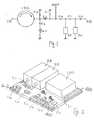
- a duplexer as shown in Fig. 1is formed according to this invention by mounting the isolator ISO, the dielectric resonators R 3 and R 4 , inductors L 1 and L 2 and capacitors C 1 - C 3 and C 6 - C 8 on a single substrate, as shown in Fig. 2.
- Grounding electrodes GNDare formed as wiring patterns both on the upper and lower surfaces of the substrate (although the bottom surface is not separately illustrated).
- terminals for connections, as well as input and output electrodesare formed also as wiring patterns on the upper and lower surfaces of the substrate.
- a duplexeris characterized as having a simplified circuit in the transmission section and being a unified structure including an isolator. Since the transmission section can thus be formed without using a dielectric resonator and an isolator is included as a part of the unified structure, not only dielectric resonators but also inductors and capacitors which would be required to be connected to such dielectric resonators to form a filter are no longer required. As a result, the total number of components to be assembled (and soldered) is reduced and the insertion loss can also be reduced according to this invention.
- Fig. 3shows another duplexer embodying this invention characterized as having its transmission section formed by connecting an isolator ISO to an input terminal TX and connecting a II-type low-pass filter comprised of an inductor L1 and capacitors C 1 and C 2 and a series-connected trap circuit comprising a dielectric resonator R 2 and a capacitor C 3 between the isolator ISO and the antenna terminal ANT.
- Its reception sectionis structured as explained above with reference to Fig. 1.
- the duplexer shown in Fig. 3may be described as using the dielectric resonator R 2 in the place of the inductor L 2 of Fig. 1.
- the circuit for the transmission sectioncomposed of the inductor L 1 , capacitors C 1 , C 2 and C 3 and the dielectric resonator R 2 is for the purpose of matching the isolator in the transmission section with the receiving circuit at a receiving station.
- a duplexer according to the second embodiment of the inventionis characterized wherein its transmission section does not have the filtering function obtainable with a plurality of dielectric resonators which were necessary in prior art duplexer for obtaining attenuation. Instead, the transmission section includes only one dielectric resonator, and it is for the purpose of matching. Thus, the transmission section is much simplified as compared to prior art duplexers.
- a duplexer according to this inventionis characterized in that all these components shown in Fig. 3, inclusive of the isolator, are mounted on a single substrate, as shown in Fig. 2. Since use is made of a single substrate and the transmission section includes only one dielectric resonator for matching, the total number of components, as well as the insertion loss, can be reduced also according to this embodiment of this invention.
- the circuit for the reception sectionmay be formed with a single-stage dielectric resonator or a multi-stage resonator apparatus with three or more stages.
- the manner of connecting the resonatorsis not intended to limit the scope of the invention.
- dielectric resonatorseach comprising a dielectric block having a throughhole serving as a resonator
- a dielectric resonator apparatusor dielectric filter
- Duplexers according to this inventionare finally characterized as having a simplified circuit for its transmission section and every component inclusive of an isolator mounted on a single substrate such that they can be easily mounted on a circuit board for an apparatus such as a portable telephone and the cost of the mounting can be reduced. Since the transmission section can be formed without using any dielectric resonator or only one dielectric resonator, furthermore, the total number of the components can be reduced significantly. As a result, the insertion loss is reduced, the duplexer can be made compact and the cost of parts as well as the overall production cost can be significantly reduced.
Landscapes
- Control Of Motors That Do Not Use Commutators (AREA)
Description
- This invention relates to a duplexer, usable in amobile communication apparatus such as a car phone anda portable phone, for allowing a single antenna to beused for both transmission and reception of signals.
- There is a trend for compactness and high-densitymounting in mobile communication apparatus such asportable telephones, and the progress is in thedirection of digital systems. Under thesecircumstances, there are increased demands forcompactness and high-density mounting for the componentswhich are used in such apparatus.
- An antenna circuit for an apparatus such as aportable telephone is generally structured, as shown inFig. 4, by connecting an isolator ISO to a duplexer, theduplexer being composed of a transmission filter and areception filter and the isolator being connected to theinput terminal of its transmission section. Fig. 5shows a circuit diagram of a duplexer for a prior artmobile communication apparatus such as a portable analogtelephone using dielectric resonators. Its transmissionsection comprises a band elimination filter using twodielectric resonators R1 and R2 as well as capacitors C1- C5 and inductors L1 and L3, and its reception sectioncomprises a two-stage bandpass filter using twodielectric resonators R3 and R4 as well as capacitors C6- C8. An antenna terminal ANT in the middle isconnected to an antenna. The inductor L1 and the capacitors C1 and C2 together form a Π-type low-pass filter adapted to adjust the phaseat the antenna terminal ANT of the band elimination filter such that the impedance becomes an open circuit in the pass band of the bandpass filter in the reception section.The dielectric resonators R1 - R4, capacitors C1 -C8 and inductors L1 -3 are mounted on a single substrate to form a duplexer of a unifiedstructure and, when it is used in an apparatus such as a portable telephone, such aduplexer and an isolator are mounted separately on a circuit board.
- Thus, a prior art duplexer has a transmission section having a filtering functionwith large attenuation in the pass band of the reception section, and use is therefore madeof a dielectric filter with large attenuation comprising a plurality of dielectric resonators.Thus, many dielectric resonators, capacitance-providing elements and inductance-providingelements such as coils were required. This makes it difficult to provide acompact duplexer, and since these many elements must be properly arranged andsoldered, not only the cost of components but the cost of production is increased.Moreover, such a prior art duplexer has the problem of a large insertion loss.
- It is therefore an object of this invention to eliminate the problems as describedabove of prior art duplexers and to provide an improved duplexer with a small loss, whichis composed of an isolator and a fewer components, can be produced at a reduced costand in a compact form, can be mounted on a circuit board easily and requires a reducedarea for mounting.
- According to the present invention, there is provided a duplexer comprising:
- a transmission section comprising an isolator and a transmission circuit comprisingat least one inductor and capacitors; and
- a reception section comprising a reception filter having a dielectric resonatorapparatus; characterized in that said transmission section has the function of matching saidisolator with said reception filter, in that said transmission and reception sections aremounted on a single substrate, and in that
- said transmission circuit comprises a trap circuit.
- Preferably said trapcircuit comprises a series connected resonance circuit having a inductor and a capacitor.
- Alternatively, said trap circuit comprises a series connected resonance circuithaving a dielectric resonator and a capacitor.
- Preferably, said transmission circuit comprises a Π-type low-pass filter having aninductor and capacitors.
- With a duplexer thus formed, fewer components are required because itstransmission section includes no dielectric resonators or only one dielectric resonator, anda compact duplexer with a low loss can be realized.
- The accompanying drawings, which are incorporated in and form a part of thisspecification, illustrate embodiments of the invention and, together with the description,serve to explain the principles of the invention. In the drawings:
- Fig. 1 is a circuit diagram of a duplexer embodying this invention;
- Fig. 2 is a diagonal external view of the duplexer of Fig. 1 mounted on a substrate;
- Fig. 3 is a circuit diagram of another duplexer according to another embodiment ofthe invention;
- Fig. 4 is a schematic diagram showing the general structure of a duplexer; and
- Fig. 5 is a circuit diagram of a prior art duplexer.
- Throughout herein, components which are equivalent although belonging todifferent duplexers are indicated by the same symbols for convenience.
- As shown in Fig. 1, a duplexer according to this invention has a bandpass filter inits reception section formed with capacitors C7, C8 and C6 inserted respectively betweentwo dielectric resonators R3 and R4, between the dielectric resonator R4 and an outputterminal RX, and between the dielectric resonator R3 and an antenna terminal ANT. Inits transmission section, an isolator ISO is connected to an input terminal TX, and a Π-typelow-pass filter comprised of an inductor L1 and capacitors C1 and C2 and a series-connectedtrap circuit comprising an inductor L2 and a capacitor C3 are connectedbetween the isolator ISO and the antenna terminal ANT.
- The main function of this Π-type low-pass filter comprised of the inductor L1 andcapacitors C1 and C2 and the series-connected trap circuit comprising the inductor L2 andthe capacitor C3 is to adjust the phase such that the impedance in the passband of the band pass filter at the receiving station becomes an open circuit at the antenna terminal ANT. Inother words, the circuit in the transmission section described above is for the purpose ofmatching the isolator with the reception filter and not for obtaining attenuation inside the passband, atthe receiving section.
- In summary, the circuit according to this embodiment of the invention is obtainedby replacing the prior art filter circuit using dielectric resonators (as shown in Fig. 5) by acircuit having only inductors and capacitors, and this has become possible becauseattenuation inside the passband at the receiving stationis unnecessary in the case of a duplexer comprising atransmission filter and a reception filter used for adigital portable telephone, etc.
- A duplexer as shown in Fig. 1 is formed accordingto this invention by mounting the isolator ISO, thedielectric resonators R3 and R4, inductors L1 and L2 andcapacitors C1 - C3 and C6 - C8 on a single substrate, asshown in Fig. 2. Grounding electrodes GND are formed aswiring patterns both on the upper and lower surfaces ofthe substrate (although the bottom surface is notseparately illustrated). Similarly, although not shownin Fig. 2, terminals for connections, as well as inputand output electrodes are formed also as wiring patternson the upper and lower surfaces of the substrate.
- In summary, a duplexer according to this embodimentof the invention is characterized as having a simplifiedcircuit in the transmission section and being a unifiedstructure including an isolator. Since the transmissionsection can thus be formed without using a dielectricresonator and an isolator is included as a part of theunified structure, not only dielectric resonators butalso inductors and capacitors which would be required tobe connected to such dielectric resonators to form afilter are no longer required. As a result, the totalnumber of components to be assembled (and soldered) isreduced and the insertion loss can also be reducedaccording to this invention.
- Fig. 3 shows another duplexer embodying thisinvention characterized as having its transmissionsection formed by connecting an isolator ISO to an inputterminal TX and connecting a II-type low-pass filtercomprised of an inductor L1 and capacitors C1 and C2 anda series-connected trap circuit comprising a dielectric resonator R2 and a capacitor C3 between the isolator ISOand the antenna terminal ANT. Its reception section isstructured as explained above with reference to Fig. 1.In other words, the duplexer shown in Fig. 3 may bedescribed as using the dielectric resonator R2 in theplace of the inductor L2 of Fig. 1. Thus, the circuitfor the transmission section composed of the inductorL1, capacitors C1, C2 and C3 and the dielectric resonatorR2 is for the purpose of matching the isolator in thetransmission section with the receiving circuit at areceiving station.
- As explained above, a duplexer according to thesecond embodiment of the invention is characterizedwherein its transmission section does not have thefiltering function obtainable with a plurality ofdielectric resonators which were necessary in prior artduplexer for obtaining attenuation. Instead, thetransmission section includes only one dielectricresonator, and it is for the purpose of matching. Thus,the transmission section is much simplified as comparedto prior art duplexers.
- Although not separately illustrated, a duplexeraccording to this invention, of which the circuitdiagram is shown in Fig. 3, is characterized in that allthese components shown in Fig. 3, inclusive of theisolator, are mounted on a single substrate, as shown inFig. 2. Since use is made of a single substrate and thetransmission section includes only one dielectric resonatorfor matching, the total number of components, as well asthe insertion loss, can be reduced also according tothis embodiment of this invention.
- Although this invention has been described above interms of only a limited number of examples, theinvention is not intended to be limited by theseillustrated examples. Many modifications and variations are possible within the scope of the invention. Forexample, although the illustrated examples included atwo-stage resonator apparatus for the reception section,the circuit for the reception section may be formed witha single-stage dielectric resonator or a multi-stageresonator apparatus with three or more stages. Themanner of connecting the resonators is not intended tolimit the scope of the invention. As another example,although a plurality of dielectric resonators, eachcomprising a dielectric block having a throughholeserving as a resonator, are used as a filter for thereception section in the illustrated examples, use mayequally well be made of a dielectric resonator apparatus(or dielectric filter) comprising a single dielectricblock having a plurality of throughholes serving asresonators. In summary, all such modifications andvariations that are obvious to a person skilled in theart are intended to be within the scope of theinvention. Duplexers according to this invention arefinally characterized as having a simplified circuit forits transmission section and every component inclusiveof an isolator mounted on a single substrate such thatthey can be easily mounted on a circuit board for anapparatus such as a portable telephone and the cost ofthe mounting can be reduced. Since the transmissionsection can be formed without using any dielectricresonator or only one dielectric resonator, furthermore,the total number of the components can be reducedsignificantly. As a result, the insertion loss isreduced, the duplexer can be made compact and the costof parts as well as the overall production cost can besignificantly reduced.
Claims (4)
- A duplexer comprising:characterized in that said transmission section has the function of matching saidisolator with said reception filter, in that said transmission and reception sections aremounted on a single substrate, anda transmission section comprising an isolator (ISO) and a transmission circuitcomprising at least one inductor (L1) and capacitors (C1, C2, C3); anda reception section comprising a reception filter having a dielectric resonatorapparatus;in that said transmission circuitcomprises a trap circuit.
- A duplexer according to claim 1, characterized in that said trap circuit comprises aseries connected resonance circuit having a inductor (L2) and a capacitor (C3).
- A duplexer according to claim 1, characterized in that said trap circuit comprises aseries connected resonance circuit having a dielectric resonator (R2) and a capacitor (C3).
- A duplexer according to any one of claims 1 to 3, characterized in thatsaid transmission circuit comprises a Π-type low-pass filter having an inductor(L1), and capacitors (C1, C2).
Applications Claiming Priority (3)
| Application Number | Priority Date | Filing Date | Title |
|---|---|---|---|
| JP8852494 | 1994-04-26 | ||
| JP08852494AJP3316713B2 (en) | 1994-04-26 | 1994-04-26 | Antenna duplexer |
| JP88524/94 | 1994-04-26 |
Publications (2)
| Publication Number | Publication Date |
|---|---|
| EP0680108A1 EP0680108A1 (en) | 1995-11-02 |
| EP0680108B1true EP0680108B1 (en) | 1999-12-08 |
Family
ID=13945231
Family Applications (1)
| Application Number | Title | Priority Date | Filing Date |
|---|---|---|---|
| EP95302705AExpired - LifetimeEP0680108B1 (en) | 1994-04-26 | 1995-04-24 | Duplexer |
Country Status (5)
| Country | Link |
|---|---|
| US (1) | US5604470A (en) |
| EP (1) | EP0680108B1 (en) |
| JP (1) | JP3316713B2 (en) |
| DE (1) | DE69513719T2 (en) |
| TW (1) | TW269060B (en) |
Cited By (7)
| Publication number | Priority date | Publication date | Assignee | Title |
|---|---|---|---|---|
| US7071776B2 (en) | 2001-10-22 | 2006-07-04 | Kyocera Wireless Corp. | Systems and methods for controlling output power in a communication device |
| US7116954B2 (en) | 2001-04-11 | 2006-10-03 | Kyocera Wireless Corp. | Tunable bandpass filter and method thereof |
| US7154440B2 (en) | 2001-04-11 | 2006-12-26 | Kyocera Wireless Corp. | Phase array antenna using a constant-gain phase shifter |
| US7174147B2 (en) | 2001-04-11 | 2007-02-06 | Kyocera Wireless Corp. | Bandpass filter with tunable resonator |
| US7221243B2 (en) | 2001-04-11 | 2007-05-22 | Kyocera Wireless Corp. | Apparatus and method for combining electrical signals |
| US7248845B2 (en) | 2004-07-09 | 2007-07-24 | Kyocera Wireless Corp. | Variable-loss transmitter and method of operation |
| US7548762B2 (en) | 2005-11-30 | 2009-06-16 | Kyocera Corporation | Method for tuning a GPS antenna matching network |
Families Citing this family (25)
| Publication number | Priority date | Publication date | Assignee | Title |
|---|---|---|---|---|
| WO1997004534A1 (en)* | 1995-07-14 | 1997-02-06 | Lg Products Ab | Amplifier for antennas |
| JP3309271B2 (en)* | 1996-07-09 | 2002-07-29 | 京セラ株式会社 | Mobile terminal |
| JPH11122139A (en)* | 1997-10-17 | 1999-04-30 | Murata Mfg Co Ltd | Antenna multicoupler |
| US6049702A (en)* | 1997-12-04 | 2000-04-11 | Rockwell Science Center, Llc | Integrated passive transceiver section |
| JP2000134130A (en) | 1998-10-22 | 2000-05-12 | Matsushita Electric Ind Co Ltd | Transmission / reception switch |
| JP2000151228A (en)* | 1998-11-09 | 2000-05-30 | Murata Mfg Co Ltd | Resonator device, oscillator, filter, duplexer and communication device |
| US7346374B2 (en) | 1999-05-26 | 2008-03-18 | Johnson Controls Technology Company | Wireless communications system and method |
| EP1246414B1 (en) | 1999-05-26 | 2012-05-23 | Johnson Controls Technology Company | Wireless communications system and method therefor |
| KR100384399B1 (en)* | 2000-11-28 | 2003-05-22 | 주식회사 케이이씨 | Frequency isolation circuit of a duplexer |
| US7394430B2 (en) | 2001-04-11 | 2008-07-01 | Kyocera Wireless Corp. | Wireless device reconfigurable radiation desensitivity bracket systems and methods |
| US7746292B2 (en) | 2001-04-11 | 2010-06-29 | Kyocera Wireless Corp. | Reconfigurable radiation desensitivity bracket systems and methods |
| US6937195B2 (en) | 2001-04-11 | 2005-08-30 | Kyocera Wireless Corp. | Inverted-F ferroelectric antenna |
| DE60207546T2 (en)* | 2001-04-11 | 2006-07-27 | Kyocera Wireless Corp., San Diego | ANTENNA INTERFACE UNIT |
| US7164329B2 (en) | 2001-04-11 | 2007-01-16 | Kyocera Wireless Corp. | Tunable phase shifer with a control signal generator responsive to DC offset in a mixed signal |
| JP2003158437A (en)* | 2001-09-06 | 2003-05-30 | Murata Mfg Co Ltd | Lc filter circuit, laminate type lc filter, multiplexer, and radio communication device |
| KR100456004B1 (en)* | 2001-12-17 | 2004-11-08 | 주식회사 케이이씨 | Transmission band pass filter of duplexer |
| US7180467B2 (en) | 2002-02-12 | 2007-02-20 | Kyocera Wireless Corp. | System and method for dual-band antenna matching |
| US7176845B2 (en) | 2002-02-12 | 2007-02-13 | Kyocera Wireless Corp. | System and method for impedance matching an antenna to sub-bands in a communication band |
| US7184727B2 (en) | 2002-02-12 | 2007-02-27 | Kyocera Wireless Corp. | Full-duplex antenna system and method |
| US7720443B2 (en) | 2003-06-02 | 2010-05-18 | Kyocera Wireless Corp. | System and method for filtering time division multiple access telephone communications |
| KR100715379B1 (en)* | 2005-04-22 | 2007-05-09 | 주식회사 앱솔테크 | Combined Filter |
| DE102005020086B4 (en)* | 2005-04-29 | 2013-07-11 | Epcos Ag | Electric multiband component |
| TWI252605B (en)* | 2005-05-31 | 2006-04-01 | Ind Tech Res Inst | Multilayered chip-type triplexer |
| WO2009082378A2 (en) | 2006-10-11 | 2009-07-02 | Johnson Controls Technology Company | Wireless network selection |
| TWI531108B (en)* | 2013-01-18 | 2016-04-21 | 矽品精密工業股份有限公司 | A duplexer and a circuit structure of the same and a radio frequency transceiver device |
Family Cites Families (9)
| Publication number | Priority date | Publication date | Assignee | Title |
|---|---|---|---|---|
| JPS6038884B2 (en)* | 1979-04-02 | 1985-09-03 | 島田理化工業株式会社 | Electromagnetic wave synthesizer |
| JPS61214625A (en)* | 1985-03-19 | 1986-09-24 | Tokyo Electric Co Ltd | antenna coupling circuit |
| US5023866A (en)* | 1987-02-27 | 1991-06-11 | Motorola, Inc. | Duplexer filter having harmonic rejection to control flyback |
| US5015973A (en)* | 1987-08-31 | 1991-05-14 | Oki Electric Industry Co., Ltd. | Duplexer with an isolating circuit on a dielectric plate |
| JPH01198802A (en)* | 1987-10-07 | 1989-08-10 | Murata Mfg Co Ltd | Irreversible circuit element |
| JPH0362626A (en)* | 1989-07-31 | 1991-03-18 | Nec Corp | Radio transmitter-receiver |
| US5293141A (en)* | 1991-03-25 | 1994-03-08 | Sanyo Electric Co., Ltd. | Dielectric filter having external connection terminals on dielectric substrate and antenna duplexer using the same |
| JPH04304003A (en)* | 1991-04-01 | 1992-10-27 | Murata Mfg Co Ltd | Multicoupler |
| JPH0795112A (en)* | 1993-09-20 | 1995-04-07 | Fujitsu Ltd | Digital mobile radio equipment |
- 1994
- 1994-04-26JPJP08852494Apatent/JP3316713B2/ennot_activeExpired - Lifetime
- 1995
- 1995-04-13USUS08/422,143patent/US5604470A/ennot_activeExpired - Lifetime
- 1995-04-24DEDE69513719Tpatent/DE69513719T2/ennot_activeExpired - Lifetime
- 1995-04-24EPEP95302705Apatent/EP0680108B1/ennot_activeExpired - Lifetime
- 1995-05-02TWTW084104381Apatent/TW269060B/zhnot_activeIP Right Cessation
Cited By (9)
| Publication number | Priority date | Publication date | Assignee | Title |
|---|---|---|---|---|
| US7116954B2 (en) | 2001-04-11 | 2006-10-03 | Kyocera Wireless Corp. | Tunable bandpass filter and method thereof |
| US7154440B2 (en) | 2001-04-11 | 2006-12-26 | Kyocera Wireless Corp. | Phase array antenna using a constant-gain phase shifter |
| US7174147B2 (en) | 2001-04-11 | 2007-02-06 | Kyocera Wireless Corp. | Bandpass filter with tunable resonator |
| US7221327B2 (en) | 2001-04-11 | 2007-05-22 | Kyocera Wireless Corp. | Tunable matching circuit |
| US7221243B2 (en) | 2001-04-11 | 2007-05-22 | Kyocera Wireless Corp. | Apparatus and method for combining electrical signals |
| US7509100B2 (en) | 2001-04-11 | 2009-03-24 | Kyocera Wireless Corp. | Antenna interface unit |
| US7071776B2 (en) | 2001-10-22 | 2006-07-04 | Kyocera Wireless Corp. | Systems and methods for controlling output power in a communication device |
| US7248845B2 (en) | 2004-07-09 | 2007-07-24 | Kyocera Wireless Corp. | Variable-loss transmitter and method of operation |
| US7548762B2 (en) | 2005-11-30 | 2009-06-16 | Kyocera Corporation | Method for tuning a GPS antenna matching network |
Also Published As
| Publication number | Publication date |
|---|---|
| DE69513719T2 (en) | 2000-04-06 |
| EP0680108A1 (en) | 1995-11-02 |
| US5604470A (en) | 1997-02-18 |
| JPH07297605A (en) | 1995-11-10 |
| DE69513719D1 (en) | 2000-01-13 |
| TW269060B (en) | 1996-01-21 |
| JP3316713B2 (en) | 2002-08-19 |
Similar Documents
| Publication | Publication Date | Title |
|---|---|---|
| EP0680108B1 (en) | Duplexer | |
| AU701172B2 (en) | Radio communication transceiver | |
| US6222426B1 (en) | Branching filter with a composite circuit of an LC circuit and a serial arm saw resonator | |
| US6919782B2 (en) | Filter structure including circuit board | |
| EP1432133B1 (en) | Duplexer and communication apparatus | |
| EP1944867B1 (en) | Elastic wave filter apparatus | |
| US20070159274A1 (en) | SAW filter and portable terminal | |
| US7579927B2 (en) | Duplexer | |
| EP1508974A2 (en) | Antenna duplexer and mobile communication device using the same | |
| CN213937873U (en) | High-frequency module and communication device | |
| CN1852026B (en) | Filter and duplexer | |
| KR0139477B1 (en) | Dielectric filter | |
| EP0468757A2 (en) | Branching filter | |
| US6373350B1 (en) | Branching filter with saw-resonator transmitting and receiving filters in separate packages and receiving-branch lines in both packages | |
| JPH10294634A (en) | Filter | |
| US5977848A (en) | Polar dielectric filter and dielectric duplexer incorporating same | |
| JPH07231241A (en) | Surface acoustic wave device | |
| KR200167764Y1 (en) | Duplexer | |
| US6249194B1 (en) | Composite filter comprising LC and saw filters and radio communication apparatus using the filter | |
| US6816032B1 (en) | Laminated low-profile dual filter module for telecommunications devices and method therefor | |
| US6369668B1 (en) | Duplexer and communication apparatus including the same | |
| EP0812065B1 (en) | Active filter | |
| JP3398243B2 (en) | Antenna duplexer | |
| JPH08111604A (en) | Dielectric filter | |
| KR19990049687A (en) | Duplex dielectric filter |
Legal Events
| Date | Code | Title | Description |
|---|---|---|---|
| PUAI | Public reference made under article 153(3) epc to a published international application that has entered the european phase | Free format text:ORIGINAL CODE: 0009012 | |
| 17P | Request for examination filed | Effective date:19950428 | |
| AK | Designated contracting states | Kind code of ref document:A1 Designated state(s):DE FR GB | |
| RAP1 | Party data changed (applicant data changed or rights of an application transferred) | Owner name:MURATA MANUFACTURING CO. LTD. | |
| 17Q | First examination report despatched | Effective date:19971021 | |
| GRAG | Despatch of communication of intention to grant | Free format text:ORIGINAL CODE: EPIDOS AGRA | |
| GRAG | Despatch of communication of intention to grant | Free format text:ORIGINAL CODE: EPIDOS AGRA | |
| GRAH | Despatch of communication of intention to grant a patent | Free format text:ORIGINAL CODE: EPIDOS IGRA | |
| GRAH | Despatch of communication of intention to grant a patent | Free format text:ORIGINAL CODE: EPIDOS IGRA | |
| GRAA | (expected) grant | Free format text:ORIGINAL CODE: 0009210 | |
| AK | Designated contracting states | Kind code of ref document:B1 Designated state(s):DE FR GB | |
| REF | Corresponds to: | Ref document number:69513719 Country of ref document:DE Date of ref document:20000113 | |
| ET | Fr: translation filed | ||
| PLBE | No opposition filed within time limit | Free format text:ORIGINAL CODE: 0009261 | |
| STAA | Information on the status of an ep patent application or granted ep patent | Free format text:STATUS: NO OPPOSITION FILED WITHIN TIME LIMIT | |
| 26N | No opposition filed | ||
| REG | Reference to a national code | Ref country code:GB Ref legal event code:IF02 | |
| PGFP | Annual fee paid to national office [announced via postgrant information from national office to epo] | Ref country code:GB Payment date:20140423 Year of fee payment:20 | |
| PGFP | Annual fee paid to national office [announced via postgrant information from national office to epo] | Ref country code:FR Payment date:20140409 Year of fee payment:20 Ref country code:DE Payment date:20140430 Year of fee payment:20 | |
| REG | Reference to a national code | Ref country code:DE Ref legal event code:R071 Ref document number:69513719 Country of ref document:DE | |
| REG | Reference to a national code | Ref country code:GB Ref legal event code:PE20 Expiry date:20150423 | |
| PG25 | Lapsed in a contracting state [announced via postgrant information from national office to epo] | Ref country code:GB Free format text:LAPSE BECAUSE OF EXPIRATION OF PROTECTION Effective date:20150423 |