EP0680072B1 - A method of operating a high density plasma CVD reactor with combined inductive and capacitive coupling - Google Patents
A method of operating a high density plasma CVD reactor with combined inductive and capacitive couplingDownload PDFInfo
- Publication number
- EP0680072B1 EP0680072B1EP95302801AEP95302801AEP0680072B1EP 0680072 B1EP0680072 B1EP 0680072B1EP 95302801 AEP95302801 AEP 95302801AEP 95302801 AEP95302801 AEP 95302801AEP 0680072 B1EP0680072 B1EP 0680072B1
- Authority
- EP
- European Patent Office
- Prior art keywords
- chamber
- ceiling electrode
- coil antenna
- reactor
- wafer
- Prior art date
- Legal status (The legal status is an assumption and is not a legal conclusion. Google has not performed a legal analysis and makes no representation as to the accuracy of the status listed.)
- Expired - Lifetime
Links
- 238000000034methodMethods0.000titleclaimsabstractdescription29
- 230000008878couplingEffects0.000titleabstractdescription26
- 238000010168coupling processMethods0.000titleabstractdescription26
- 238000005859coupling reactionMethods0.000titleabstractdescription26
- 230000001939inductive effectEffects0.000titleabstractdescription18
- 238000005268plasma chemical vapour depositionMethods0.000titledescription4
- 238000004140cleaningMethods0.000claimsabstractdescription37
- NJPPVKZQTLUDBO-UHFFFAOYSA-NnovaluronChemical compoundC1=C(Cl)C(OC(F)(F)C(OC(F)(F)F)F)=CC=C1NC(=O)NC(=O)C1=C(F)C=CC=C1FNJPPVKZQTLUDBO-UHFFFAOYSA-N0.000claimsdescription42
- 239000007789gasSubstances0.000claimsdescription23
- 238000005530etchingMethods0.000claimsdescription6
- UFHFLCQGNIYNRP-UHFFFAOYSA-NHydrogenChemical compound[H][H]UFHFLCQGNIYNRP-UHFFFAOYSA-N0.000claimsdescription5
- 239000001257hydrogenSubstances0.000claimsdescription4
- 229910052739hydrogenInorganic materials0.000claimsdescription4
- 125000001153fluoro groupChemical groupF*0.000claimsdescription2
- GVGCUCJTUSOZKP-UHFFFAOYSA-Nnitrogen trifluorideChemical classFN(F)FGVGCUCJTUSOZKP-UHFFFAOYSA-N0.000claims1
- ABTOQLMXBSRXSM-UHFFFAOYSA-Nsilicon tetrafluorideChemical classF[Si](F)(F)FABTOQLMXBSRXSM-UHFFFAOYSA-N0.000claims1
- TXEYQDLBPFQVAA-UHFFFAOYSA-NtetrafluoromethaneChemical classFC(F)(F)FTXEYQDLBPFQVAA-UHFFFAOYSA-N0.000claims1
- 238000009616inductively coupled plasmaMethods0.000abstractdescription18
- 238000005229chemical vapour depositionMethods0.000abstractdescription12
- 238000002347injectionMethods0.000abstractdescription5
- 239000007924injectionSubstances0.000abstractdescription5
- 238000000151depositionMethods0.000abstractdescription4
- 230000008021depositionEffects0.000abstractdescription4
- 239000002243precursorSubstances0.000abstract2
- 210000002381plasmaAnatomy0.000description63
- VYPSYNLAJGMNEJ-UHFFFAOYSA-NSilicium dioxideChemical compoundO=[Si]=OVYPSYNLAJGMNEJ-UHFFFAOYSA-N0.000description34
- 235000012239silicon dioxideNutrition0.000description22
- 229910052751metalInorganic materials0.000description11
- 239000002184metalSubstances0.000description11
- 239000010453quartzSubstances0.000description11
- 239000000377silicon dioxideSubstances0.000description11
- 150000002500ionsChemical class0.000description8
- KLZUFWVZNOTSEM-UHFFFAOYSA-KAluminium flourideChemical classF[Al](F)FKLZUFWVZNOTSEM-UHFFFAOYSA-K0.000description6
- 238000004544sputter depositionMethods0.000description6
- 239000004065semiconductorSubstances0.000description5
- 239000000463materialSubstances0.000description4
- 229910021420polycrystalline siliconInorganic materials0.000description4
- 229920005591polysiliconPolymers0.000description4
- BLRPTPMANUNPDV-UHFFFAOYSA-NSilaneChemical compound[SiH4]BLRPTPMANUNPDV-UHFFFAOYSA-N0.000description3
- XUIMIQQOPSSXEZ-UHFFFAOYSA-NSiliconChemical compound[Si]XUIMIQQOPSSXEZ-UHFFFAOYSA-N0.000description3
- 229910052782aluminiumInorganic materials0.000description3
- XAGFODPZIPBFFR-UHFFFAOYSA-NaluminiumChemical compound[Al]XAGFODPZIPBFFR-UHFFFAOYSA-N0.000description3
- 238000009826distributionMethods0.000description3
- 229910000077silaneInorganic materials0.000description3
- 229910052710siliconInorganic materials0.000description3
- 239000010703siliconSubstances0.000description3
- IRPGOXJVTQTAAN-UHFFFAOYSA-N2,2,3,3,3-pentafluoropropanalChemical compoundFC(F)(F)C(F)(F)C=OIRPGOXJVTQTAAN-UHFFFAOYSA-N0.000description2
- KRHYYFGTRYWZRS-UHFFFAOYSA-MFluoride anionChemical compound[F-]KRHYYFGTRYWZRS-UHFFFAOYSA-M0.000description2
- YCKRFDGAMUMZLT-UHFFFAOYSA-NFluorine atomChemical compound[F]YCKRFDGAMUMZLT-UHFFFAOYSA-N0.000description2
- QVGXLLKOCUKJST-UHFFFAOYSA-Natomic oxygenChemical compound[O]QVGXLLKOCUKJST-UHFFFAOYSA-N0.000description2
- 230000015572biosynthetic processEffects0.000description2
- 239000000919ceramicSubstances0.000description2
- 238000011109contaminationMethods0.000description2
- 229910052731fluorineInorganic materials0.000description2
- 239000011737fluorineSubstances0.000description2
- 239000001301oxygenSubstances0.000description2
- 229910052760oxygenInorganic materials0.000description2
- 238000001020plasma etchingMethods0.000description2
- 238000009825accumulationMethods0.000description1
- 230000009286beneficial effectEffects0.000description1
- 239000003990capacitorSubstances0.000description1
- 230000015556catabolic processEffects0.000description1
- 229910010293ceramic materialInorganic materials0.000description1
- 239000011248coating agentSubstances0.000description1
- 238000000576coating methodMethods0.000description1
- 150000001875compoundsChemical class0.000description1
- 239000004020conductorSubstances0.000description1
- 239000000356contaminantSubstances0.000description1
- 238000001816coolingMethods0.000description1
- 239000012809cooling fluidSubstances0.000description1
- PMHQVHHXPFUNSP-UHFFFAOYSA-Mcopper(1+);methylsulfanylmethane;bromideChemical compoundBr[Cu].CSCPMHQVHHXPFUNSP-UHFFFAOYSA-M0.000description1
- 238000005137deposition processMethods0.000description1
- 238000010494dissociation reactionMethods0.000description1
- 230000005593dissociationsEffects0.000description1
- 230000005684electric fieldEffects0.000description1
- 230000002349favourable effectEffects0.000description1
- -1for exampleInorganic materials0.000description1
- 238000011065in-situ storageMethods0.000description1
- 239000012212insulatorSubstances0.000description1
- 238000004518low pressure chemical vapour depositionMethods0.000description1
- 238000004519manufacturing processMethods0.000description1
- 230000000873masking effectEffects0.000description1
- 239000000203mixtureSubstances0.000description1
- TWNQGVIAIRXVLR-UHFFFAOYSA-Noxo(oxoalumanyloxy)alumaneChemical compoundO=[Al]O[Al]=OTWNQGVIAIRXVLR-UHFFFAOYSA-N0.000description1
- 230000000737periodic effectEffects0.000description1
- 229920000642polymerPolymers0.000description1
- 239000010909process residueSubstances0.000description1
- 229910052814silicon oxideInorganic materials0.000description1
- 239000012686silicon precursorSubstances0.000description1
Images
Classifications
- H—ELECTRICITY
- H01—ELECTRIC ELEMENTS
- H01J—ELECTRIC DISCHARGE TUBES OR DISCHARGE LAMPS
- H01J37/00—Discharge tubes with provision for introducing objects or material to be exposed to the discharge, e.g. for the purpose of examination or processing thereof
- H01J37/32—Gas-filled discharge tubes
- H01J37/32431—Constructional details of the reactor
- H01J37/32798—Further details of plasma apparatus not provided for in groups H01J37/3244 - H01J37/32788; special provisions for cleaning or maintenance of the apparatus
- H01J37/32853—Hygiene
- H01J37/32862—In situ cleaning of vessels and/or internal parts
- H—ELECTRICITY
- H01—ELECTRIC ELEMENTS
- H01L—SEMICONDUCTOR DEVICES NOT COVERED BY CLASS H10
- H01L21/00—Processes or apparatus adapted for the manufacture or treatment of semiconductor or solid state devices or of parts thereof
- H01L21/02—Manufacture or treatment of semiconductor devices or of parts thereof
- H01L21/04—Manufacture or treatment of semiconductor devices or of parts thereof the devices having potential barriers, e.g. a PN junction, depletion layer or carrier concentration layer
- H01L21/18—Manufacture or treatment of semiconductor devices or of parts thereof the devices having potential barriers, e.g. a PN junction, depletion layer or carrier concentration layer the devices having semiconductor bodies comprising elements of Group IV of the Periodic Table or AIIIBV compounds with or without impurities, e.g. doping materials
- H01L21/30—Treatment of semiconductor bodies using processes or apparatus not provided for in groups H01L21/20 - H01L21/26
- H01L21/302—Treatment of semiconductor bodies using processes or apparatus not provided for in groups H01L21/20 - H01L21/26 to change their surface-physical characteristics or shape, e.g. etching, polishing, cutting
- C—CHEMISTRY; METALLURGY
- C23—COATING METALLIC MATERIAL; COATING MATERIAL WITH METALLIC MATERIAL; CHEMICAL SURFACE TREATMENT; DIFFUSION TREATMENT OF METALLIC MATERIAL; COATING BY VACUUM EVAPORATION, BY SPUTTERING, BY ION IMPLANTATION OR BY CHEMICAL VAPOUR DEPOSITION, IN GENERAL; INHIBITING CORROSION OF METALLIC MATERIAL OR INCRUSTATION IN GENERAL
- C23C—COATING METALLIC MATERIAL; COATING MATERIAL WITH METALLIC MATERIAL; SURFACE TREATMENT OF METALLIC MATERIAL BY DIFFUSION INTO THE SURFACE, BY CHEMICAL CONVERSION OR SUBSTITUTION; COATING BY VACUUM EVAPORATION, BY SPUTTERING, BY ION IMPLANTATION OR BY CHEMICAL VAPOUR DEPOSITION, IN GENERAL
- C23C16/00—Chemical coating by decomposition of gaseous compounds, without leaving reaction products of surface material in the coating, i.e. chemical vapour deposition [CVD] processes
- C23C16/44—Chemical coating by decomposition of gaseous compounds, without leaving reaction products of surface material in the coating, i.e. chemical vapour deposition [CVD] processes characterised by the method of coating
- C23C16/4401—Means for minimising impurities, e.g. dust, moisture or residual gas, in the reaction chamber
- C23C16/4405—Cleaning of reactor or parts inside the reactor by using reactive gases
- H—ELECTRICITY
- H01—ELECTRIC ELEMENTS
- H01J—ELECTRIC DISCHARGE TUBES OR DISCHARGE LAMPS
- H01J37/00—Discharge tubes with provision for introducing objects or material to be exposed to the discharge, e.g. for the purpose of examination or processing thereof
- H01J37/32—Gas-filled discharge tubes
- H01J37/32009—Arrangements for generation of plasma specially adapted for examination or treatment of objects, e.g. plasma sources
- H01J37/32082—Radio frequency generated discharge
Definitions
- the inventionis related to a method of operating a high density plasma CVD reactor having inductive and capacitive coupling modes which can be selected individually or in combination for chamber cleaning operations.
- Plasma reactors used for semiconductor processessuch as chemical vapor deposition (CVD), etching, reactive ion etching and so forth typically employ either inductive coupling or capacitive coupling to strike and maintain a plasma.
- an etch reactoremploys capacitive coupling because the high ion energies characteristic of capacitively coupled plasmas are suitable for removing films such as, for example, silicon dioxide.
- the high ion energiesarise from the high electric fields required to strike a capacitively coupled plasma.
- a capacitively coupled reactorhas parallel electrodes, including a pedestal.
- a CVD plasma reactorof the type disclosed in U.S. Patent Application Serial No. 08/113,776 entitled “High Density Plasma CVD and Etching Reactor” filed August 27, 1993 by Fairbaim and Nowak employs inductive coupling to strike and maintain the plasma.
- a domed-shaped helical coil in a dome-shaped chamber ceilingperforms the inductive coupling to the plasma at a low chamber pressure (below 13.332237 Pa or 100 milliTorr), the dome shape providing a more uniform ion density distribution across the semiconductor wafer.
- a low chamber pressurebelow 13.332237 Pa or 100 milliTorr
- Such an inductively coupled plasmais characterized by a high ion density and is therefore suitable for low pressure CVD plasma processing at high processing (e.g., deposition) rates.
- An inductively coupled plasmahas a plasma density which is up to two orders of magnitude higher, thereby providing higher processing rates.
- a capacitively coupled plasmahas a higher electrode sheet voltage, higher self-biasing and higher plasma impedance, and therefore provides higher sputtering rates and greater risk of damage to the wafer.
- An inductively coupled plasmaexhibits lower ion energy distribution, providing a lower risk of damage to the wafer.
- silicon dioxideis deposited onto the chamber walls and ceiling as well as other parts of the reactor chamber, changing the characteristics of the chamber and giving rise to particulate contamination. Therefore, the reactor chamber must be cleaned periodically to remove all such deposits and residue therefrom. Removal of silicon dioxide deposits is accomplished by introducing a fluoride-containing etchant gas such as NF 3 (for example) into the chamber and striking a plasma to perform a chamber cleaning operation.
- a fluoride-containing etchant gassuch as NF 3 (for example)
- inductively coupled plasma reactorsrequire more time to perform a chamber cleaning operation due to their larger volumes, low operational pressure, non-conductive ceilings and lack of bias of the chamber wall surfaces. Certain residues, such as silicon dioxide, typically have relatively low etch rates at low ion energies, and therefore can be difficult to remove by inductively coupled plasmas.
- some metal surfacesare thoroughly cleansed of residue or deposits before others, and the cleaned metal surfaces (e.g., aluminum) are etched while the remaining contaminants are removed from the other still-unclean surfaces.
- the edge of the ceiling electrodequickly becomes clean while the center portion still has a thick residue coating remaining thereon.
- the exposed metal surface of the electrode edgeshunts RF energy away from the still-unclean center portion, thereby preventing any further cleaning of the center portion.
- a fluoride gassuch as NF 3
- the metal surfacesreact with the etchant gas during the cleaning operation to form various aluminum fluorides, which redeposit onto various chamber surfaces, including the ones that are still unclean with other residues or deposits.
- Such aluminum fluoridesetch very slowly or are virtually impervious to being etched (particularly in an inductively coupled plasma), thus masking the prior deposits (e.g., silicon dioxide) underneath. This deposition of aluminum fluorides during the cleaning operation prevents the removal of the remaining residues (e.g., silicon dioxide), so that the reactor chamber cannot be thoroughly cleaned, even by extending the duration of the chamber cleaning operation.
- a related problemis that some chamber dielectric surfaces (for example, quartz surfaces) are consumed rapidly during a chamber cleaning operation, particularly in an inductively coupled plasma, and must therefore be frequently replaced at great cost, a significant disadvantage.
- EP-A-0520519discloses a method of operating a plasma reactor having a vacuum chamber, a wafer-holding pedestal capable of supporting a wafer adjacent the bottom of said vacuum chamber, gas inlets, and a vacuum pump, a generally planar conductive ceiling electrode at the top of said chamber, a coil antenna disposed around a space between said ceiling electrode and said wafer-holding pedestal, and switches for individually connecting each one of said coil antenna, said ceiling electrode and said wafer pedestal to at least one of (a) a first RF power source, (b) ground, (c) a floating potential, (d) a second RF power source.
- EP-A-641 103additionally discloses said method including a chamber cleaning operation comprising steps of creating a capacitively coupled plasma processing pressure level in said chamber with said vacuum pump while introducing an etchant gas into said chamber through said gas inlets; and creating a capacitively coupled plasma in said chamber by operating a first one of said switches so as to apply RF energy to said ceiling electrode by connecting said ceiling electrode to said first RF power source.
- such a methodis characterised by initially, operating a second one of said switches so as to connect said coil antenna to one of (a) said ground, (b) said floating potential; and after said capacitively coupled plasma has been created, operating said second one of said switches so as to apply RF energy to said coil antenna by connecting said coil antenna to said second RF power source.
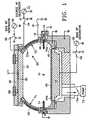
- FIG. 1is a simplified cross-sectional elevational view of a plasma reactor embodying the present invention.
- the inventionemploys a plasma reactor chamber having a dome-shaped helically coiled antenna in the side-portion of the ceiling surrounding a planar electrode in the center-portion of the ceiling.
- Meansare provided for separately coupling RF energy to the coil antenna, the ceiling electrode and the wafer pedestal at the bottom of the chamber, so that any one or combination of the ceiling electrode, the coil antenna and the wafer pedestal can receive RF energy or be grounded or be unconnected (float).
- the coil antennaprovides inductive coupling or capacitive coupling or both depending upon the type of plasma required
- the ceiling electrodeprovides capacitive coupling and, when energized simultaneously, the ceiling electrode and coil antenna together provide combined capacitive and inductive coupling to a plasma inside the reactor chamber.
- the coil antennareceives RF energy to provide an inductively coupled plasma while the ceiling electrode is grounded and an RF bias is applied to the wafer pedestal.
- RF energyis applied to the ceiling electrode to strike a capacitively coupled plasma while the wafer pedestal is permitted to electrically float (to avoid damage to the wafer pedestal and associated hardware) and the coil antenna is grounded or permitted to float.
- RF energymay be applied to the coil antenna to maintain the plasma at a higher plasma density, thus providing additional species and heat to enhance removal of silicon dioxide and similar compounds.
- RF poweris applied to the wafer pedestal while a non-production ("dummy") wafer is held on the pedestal, to strike a capacitively coupled plasma to clean the chamber.
- the top electrodeis preferably either grounded or has RF power applied to it. This method is also applicable using an inductively coupled plasma.
- the ceiling electrodeis preferably heated to a temperature on the order of between approximately 260 and 270 degrees C to increase the chamber cleaning rate.
- a capacitive plasmacan be ignited by (i) applying RF power to the ceiling electrode alone, (ii) simultaneously applying power to the ceiling electrode and the coil, and (iii) simultaneously applying RF power to the ceiling electrode, the coil and the wafer pedestal.
- RF powerto the ceiling electrode helps clean the grounded surfaces and ceiling surface fast.
- Applying power to both the ceiling electrode and the coilenhances cleaning of dielectric surfaces while cleaning the metal surfaces fast because of enhanced fluorine dissociation and higher plasma temperature.
- Applying RF power simultaneously to the ceiling electrode, the coil and the wafer pedestalreduces sputtering of the metal chamber wall surfaces by providing additional ground path(s) to the plasma.
- the choice of one of the three modes (i), (ii) and (iii) abovemay be made in accordance with the distribution of deposited oxide residue in the chamber.
- a "dummy" wafermay be kept on the wafer pedestal during chamber clean operations to protect the pedestal surface from etching. This is particularly preferred when operating in mode (iii) above.
- RF poweris applied to the coils to ignite the plasma while maintaining a certain pressure level (typically between 30 and 300 milli-Torr depending upon the applied RF power level). Once the plasma is ignited, the pressure may be reduced to less than 30 mTorr to maintain the plasma.
- a plasma reactor of the preferred embodimenthas a vacuum chamber 10, a vacuum pump 12 and gas injection nozzles 14 connected to a gas supply ring manifold 16 in a metal housing 18 supporting the injection nozzles 14.
- the chamber 10has a ceiling 20 consisting of a partial dome-shaped or hemispherical annulus 22 surrounding a planar disk 24.
- the dome-shaped annulus 22is an insulator such as quartz or a ceramic.
- the dome-shaped annulus 22supports a helically coiled RF antenna 26, one terminal of which is connectable through a capacitor to ground by a switch 30 and the other end of which is connectable to an RF source 32 through a switch 34.
- the RF source 32includes an RF generator and a conventional RF matching network (not shown).
- the ceiling 24is a conductor which is connectable to either an RF source 36 or ground through a switch 38.
- the bottom of the chamber 10may include a removable grounded conductive bottom annular ring or liner 40 which may be doped polysilicon or aluminum and a wafer pedestal 44 for holding a semiconductor wafer 45.
- a dielectric annulus 44a coplanar with the top surface of the wafer 45surrounds the wafer 45 on the pedestal 44.
- the wafer pedestal 44may include an electrostatic chuck, cooling fluid channels and other conventional features not crucial to the present invention.
- the conductive annular ring 40has a convex curved interior surface 40a facing the interior of the chamber 10 of approximately the same surface area as the ceiling electrode 24.
- This featurefacilitates capacitive discharge and exposes the chamber bottom ground surfaces toward the plasma.
- an RF sourceis applied to the ceiling electrode 24 and the annular ring 40 is grounded, both are etched at about the same rate, a significant advantage.
- the removable ring annulus liner 40is advantageous for periodic maintainance and chamber bottom cleaning.
- flat ceiling electrodestend to build up contamination (e.g., silicon dioxide) nonuniformly.
- contaminatione.g., silicon dioxide
- the depositconsists primarily of polymer which tends to deposit more on cooler unbiased surfaces, i.e., the outside edges of the ceiling electrode.
- most of the oxide depositis located in the center of the ceiling electrode across from the wafer. This is due to the sputtering component of the deposition process induced by RF bias of the wafer pedestal.
- the outer portion of the ceiling electrodeclears first during chamber clean, regardless of the plasma discharge mode.
- the ceiling electrode 24 of the reactor of the present invention(FIG. 1) is reduced to a size less than the diameter of the side wall (but preferably slightly larger than the wafer pedestal 44), thus eliminating the portion of the ceiling electrode tending to a thinner residue accumulation and therefore to etching or overcleaning.
- a related advantageis that the gently curved concave surfaces of the bottom aluminum liner 40 and the quartz dome annulus 22 eliminate sharp corners in the chamber interior which would otherwise be difficult to clean during the chamber clean operation.
- the materials of the chamber 10are selected to minimize or eliminate metal surfaces which would otherwise contribute to formation of aluminum fluorides during chamber cleaning operations.
- the ceiling electrode 24 and the bottom annular ring 40may both be silicon, for example, polysilicon doped to a resistivity less than about 0.2 ohms per centimeter.
- An advantage of polysiliconis that any silicon removed therefrom during the chamber cleaning (etch) operation is volatile and readily pumped out of the chamber 10.
- the gas injection nozzles 14are a ceramic material such as aluminum oxide or aluminum nitride.
- a skirt 46 of quartz, polysilicon, silicon or ceramiccovers the metal body 18.
- the metal body 18is grounded to reduce the possibility of arcing during chamber cleaning operations.
- the wafer pedestal 44is preferably unconnected to any electric potential (i.e., electrically floating) during chamber cleaning operations so that very little etching thereof (or formation of aluminum fluoride therefrom) occurs during chamber cleaning operations.
- the wafer pedestal 44is connectable to ground or an RF source 50, or may be electrically isolated, by a switch 52.
- the coil antenna 26may be energized simultaneously or after the ceiling electrode 24 has struck a high pressure capacitively coupled plasma in the chamber 10.
- the advantage of energizing the coil antenna 26 at this pointis that it provides an efficient means of maintaining the capacitively coupled plasma and it provides a certain amount of inductive and/or capacitive coupling to the plasma near the quartz annulus 22 so as to etch residues from the quartz annulus 22.
- This coupling modecauses the quartz material of the annulus 22 to be etched at a rate less than that of a pure low pressure inductively coupled plasma mode, a significant advantage.
- the inductive coupling provided by the coil antenna 26generates additional heat in the chamber 10.
- the ceilingitself serves as a heat sink rather than a heat source because a lid 56 covering the ceiling electrode 24 has cooling jackets 58 running throughout its interior as shown in FIG. 1.
- the cleaning rate of the ceiling electrodecan, however, be accelerated by using an external heat source such as a resistive heater 60 to raise the temperature of the ceiling electrode to between 260 and 270 degrees C, for example.
- the radius R 1 of curvature of the interior surface 22a of the quartz annulus 22was 325 cm (13")
- the radius of curvature of the interior surface of the bottom ring 40was 250 cm (9.5''-10'')
- the diameter D of the ceiling electrode 24was 225cm (9")
- the diameter of the wafer pedestal 44was 200 cm (8")
- the height of the ceiling electrode 24 from the pedestal 44was 112 cm (4.5'').
- the inventionis not limited to any particular design geometry.
- the inventionin another aspect, is embodied by certain methods of using the multi-mode coupled plasma reactor of FIG. 1.
- the plasma reactor of FIG. 1has three possible plasma coupling modes: (1) a predominantly inductively coupled plasma, (2) a predominantly capacitively coupled plasma, and (3) a mixture of both inductive and capacitive coupling simultaneously, depending upon the pressure regime, chemistry and applied RF power level.
- the reactorIn order to perform chemical vapor deposition of, for example, silicon dioxide onto a wafer 45 held on the pedestal 44, the reactor is operated in the first mode to provide an inductively coupled plasma.
- a silicon precursor gassuch as silane is introduced into the chamber 10 along with an oxygen-containing gas, using the injection nozzles 14 for the silane.
- the pump valve 12ais positioned to maintain the chamber pressure at or below 100 milliTorr.
- the ceiling electrode 24is grounded while 1000-5000 watts of RF energy at between 300kHz and 14 MHz (preferably 2.0 MHz) is applied from the RF source 32 to the coil antenna 26.
- the wafer pedestalmay be either grounded or floating or an RF bias from the RF source 50 may be applied to the pedestal 44 to generate a suitable plasma sheath voltage over the semiconductor wafer 45 held on the pedestal 44 in accordance with the techniques disclosed in the above-referenced application by Collins et al. and the above-referenced application by Fairbairn and Nowak. In some cases, it may not be necessary to ground the ceiling electrode in order to strike an inductively coupled plasma.
- the chamber pressureis set at between 0.5 and 5 Torr while between 0.5 and 3 liters per minute of a fluorine-containing gas (e.g., NF 3 , CF 4 , C 2 F 6 , etc.) and oxygen is pumped into the chamber 10.
- a fluorine-containing gase.g., NF 3 , CF 4 , C 2 F 6 , etc.
- oxygenis pumped into the chamber 10.
- the wafer pedestalis disconnected and allowed to electrically float by the switch 52, the coil antenna is initially disconnected or grounded by the switches 30, 34 while between 1000 and 5000 watts of RF energy at between 300 kHz and 14 MHz (preferably 1.8 MHz) is applied to the ceiling electrode by the RF source 36 through the switch 38.
- the coil antenna 26may be connected to the RF source 32 by the switch 34 for the following three purposes: (1) the small component of capacitive coupling provided by the coil antenna 26 efficiently maintains the capacitively coupled plasma which has already been struck, (2) the proximity of the coil antenna 26 to the quartz annulus 22 enables etching or cleaning of residue or deposits from the annulus 22 and (3) the inductive coupling of the coil antenna 26 generates heat in the chamber 10, which facilitates the removal of silicon dioxide residues from interior chamber surfaces such as the ceiling electrode 24 and the quartz material around the pedestal.
- the reactorIn order to perform a sputtering or etch-operation with purely capacitive coupling, the reactor is operated as described in the preceding paragraph, with the exception that the coil antenna remains disconnected or grounded throughout.
- the capacitive coupling modeprovides much faster etch rates because it is characterized by plasma sheath voltages on the order of 50 volts, while the inductive coupling mode is characterized by plasma sheath voltages on the order of only 5 volts.
- a hydrogen-containing plasmais struck in the chamber 10 in the same manner as described with reference to the chamber cleaning operation, with the exception that hydrogen gas (or a hydrogen-containing gas such as silane) is substituted for the NF 3 gas.
- the capacitive discharge modeis more favorable for chamber cleaning due to a higher voltage drop across the sheet in the vicinity of surface to be cleaned. This results in a higher energy of the ions impinging on the surface, thus facilitating breakdown of the silicon-oxide bond.
- the reactormay be cleaned in either regime, capacitive or inductive coupling. Matching of cleaning rates in different areas of the reactor can be achieved by proper clean regime selection. In fact, a two step clean process may be employed consisting of an inductive mode plasma dean step followed by an capacitive mode plasma clean step. Alternatively, the order of these two steps may be reversed.
- the pressureIn the capacitive clean mode the pressure has to be relatively high (greater than 0.5 Torr) to prevent excessive sputtering of the chamber walls. In the low pressure regime, plasma coupling is primarily inductive and minimal wall surface biasing occurs. The inductive discharge mode leads, however, to generally higher plasma temperatures. A capacitively coupled plasma is very efficient for cleaning the electrodes. It is the inductive enhancement of the generally capacitively coupled plasma described above that helps to clean the quartz dome and other areas of the chamber not directly biased by the capacitive discharge.
- the wafer pedestalcan be biased, grounded or floating. It is beneficial to be able to so control the pedestal potential in order to either clean the pedestal from residues or, alternatively, to protect it from overcleaning and damage.
- a key advantage of the chamber cleaning process described aboveis that for a given reactor temperature the cleaning process is five to ten times faster than the cleaning process for an inductively coupled high density plasma reactor of the type described in the above-referenced application by Fairbairn and Nowak.
- the coil antenna and the ceiling electrodemay be connected together to a common RF source whenever both are to receive RF energy simultaneously.
- the reactor of FIG. 1may be operated in a broad pressure range from below 10 milliTorr to 15 Torr, the lower pressure regimes favoring a predominantly Inductively coupled plasma and the high pressure regimes favoring a predominantly capacitively coupled plasma.
Landscapes
- Chemical & Material Sciences (AREA)
- Engineering & Computer Science (AREA)
- Physics & Mathematics (AREA)
- Plasma & Fusion (AREA)
- Analytical Chemistry (AREA)
- Metallurgy (AREA)
- Health & Medical Sciences (AREA)
- Epidemiology (AREA)
- Organic Chemistry (AREA)
- Public Health (AREA)
- Mechanical Engineering (AREA)
- Materials Engineering (AREA)
- Chemical Kinetics & Catalysis (AREA)
- General Chemical & Material Sciences (AREA)
- Power Engineering (AREA)
- Microelectronics & Electronic Packaging (AREA)
- Computer Hardware Design (AREA)
- Manufacturing & Machinery (AREA)
- General Physics & Mathematics (AREA)
- Condensed Matter Physics & Semiconductors (AREA)
- Chemical Vapour Deposition (AREA)
- Drying Of Semiconductors (AREA)
- Plasma Technology (AREA)
- ing And Chemical Polishing (AREA)
Abstract
Description
- The invention is related to a method of operating a high density plasmaCVD reactor having inductive and capacitive coupling modes which can beselected individually or in combination for chamber cleaning operations.
- Plasma reactors used for semiconductor processes such as chemicalvapor deposition (CVD), etching, reactive ion etching and so forth typicallyemploy either inductive coupling or capacitive coupling to strike and maintain aplasma. Typically, an etch reactor employs capacitive coupling because thehigh ion energies characteristic of capacitively coupled plasmas are suitable forremoving films such as, for example, silicon dioxide. The high ion energiesarise from the high electric fields required to strike a capacitively coupledplasma. For example, as disclosed in European Patent Application publicationNo. 0 552 491 A1 by Collins et al. entitled "Plasma Etch Process" publishedJuly 28, 1993, a capacitively coupled reactor has parallel electrodes, including a pedestal.
- However, the plasma density of a capacitively coupled plasma is notsufficient for performing simultaneous chemical vapor deposition (CVD) and in-situsputtering at low pressures. Accordingly, a CVD plasma reactor of the typedisclosed in U.S. Patent Application Serial No. 08/113,776 entitled "HighDensity Plasma CVD and Etching Reactor" filed August 27, 1993 by Fairbaimand Nowak employs inductive coupling to strike and maintain the plasma. Inthe Fairbairn and Nowak application, a domed-shaped helical coil in a dome-shapedchamber ceiling performs the inductive coupling to the plasma at a lowchamber pressure (below 13.332237 Pa or 100 milliTorr), the dome shape providing a moreuniform ion density distribution across the semiconductor wafer. Such aninductively coupled plasma is characterized by a high ion density and istherefore suitable for low pressure CVD plasma processing at high processing(e.g., deposition) rates.
- The main differences between capacitively coupled plasmas andinductively coupled plasmas are the following: An inductively coupled plasmahas a plasma density which is up to two orders of magnitude higher, therebyproviding higher processing rates. A capacitively coupled plasma has a higherelectrode sheet voltage, higher self-biasing and higher plasma impedance, andtherefore provides higher sputtering rates and greater risk of damage to thewafer. An inductively coupled plasma exhibits lower ion energy distribution,providing a lower risk of damage to the wafer.
- A requirement of all plasma reactors, and especially plasma CVDreactors, is that they must be cleaned periodically to remove deposits andresidue. For example, in a CVD reactor, during deposition of silicon dioxide onto a semiconductor wafer, silicon dioxide is deposited onto the chamber wallsand ceiling as well as other parts of the reactor chamber, changing thecharacteristics of the chamber and giving rise to particulate contamination.Therefore, the reactor chamber must be cleaned periodically to remove all suchdeposits and residue therefrom. Removal of silicon dioxide deposits isaccomplished by introducing a fluoride-containing etchant gas such as NF3 (forexample) into the chamber and striking a plasma to perform a chambercleaning operation.
- One limitation of inductively coupled plasma reactors is that they requiremore time to perform a chamber cleaning operation due to their larger volumes,low operational pressure, non-conductive ceilings and lack of bias of thechamber wall surfaces. Certain residues, such as silicon dioxide, typically haverelatively low etch rates at low ion energies, and therefore can be difficult toremove by inductively coupled plasmas.
- One problem with such a chamber cleaning operation is that the varioussurfaces of the reactor chamber interior are not cleaned (etched) at the samerate, due to differences in location in the chamber and differences in materials;The plasma density and ion energies are not the same at all locations in thechamber, so that differences in cleaning (etch) rates are quite typical.Moreover, during wafer processing (such as CVD processing), deposits build upmore thickly on certain chamber surfaces than on others, so that the deposit orresidue thickness is non-uniform throughout the chamber interior. For example,in the etch reactor of the Collins et al. European application referenced above,the etch-process residue is much thicker in the center of the ceiling than at theedge of the ceiling, due to plasma density non-uniformity.
- As a result, some metal surfaces are thoroughly cleansed of residue ordeposits before others, and the cleaned metal surfaces (e.g., aluminum) areetched while the remaining contaminants are removed from the other still-uncleansurfaces. For example, in the case of the flat ceiling electrode of theCollins et al. European application, the edge of the ceiling electrode quicklybecomes clean while the center portion still has a thick residue coatingremaining thereon. The exposed metal surface of the electrode edge shuntsRF energy away from the still-unclean center portion, thereby preventing anyfurther cleaning of the center portion. If a fluoride gas such as NF3 isemployed to clean the chamber, the metal surfaces react with the etchant gasduring the cleaning operation to form various aluminum fluorides, which redepositonto various chamber surfaces, including the ones that are still uncleanwith other residues or deposits. Such aluminum fluorides etch very slowly orare virtually impervious to being etched (particularly in an inductively coupledplasma), thus masking the prior deposits (e.g., silicon dioxide) underneath.This deposition of aluminum fluorides during the cleaning operation preventsthe removal of the remaining residues (e.g., silicon dioxide), so that the reactorchamber cannot be thoroughly cleaned, even by extending the duration of thechamber cleaning operation.
- A related problem is that some chamber dielectric surfaces (for example,quartz surfaces) are consumed rapidly during a chamber cleaning operation,particularly in an inductively coupled plasma, and must therefore be frequentlyreplaced at great cost, a significant disadvantage.
- EP-A-0520519 discloses a method of operating aplasma reactor having a vacuum chamber, a wafer-holdingpedestal capable of supporting a waferadjacent the bottom of said vacuum chamber, gasinlets, and a vacuum pump, a generally planarconductive ceiling electrode at the top of saidchamber, a coil antenna disposed around a spacebetween said ceiling electrode and said wafer-holdingpedestal, and switches for individually connectingeach one of said coil antenna, said ceiling electrodeand said wafer pedestal to at least one of (a) a firstRF power source, (b) ground, (c) a floating potential,(d) a second RF power source.
- EP-A-641 103 additionally discloses said methodincluding a chamber cleaning operation comprisingsteps of creating a capacitively coupled plasmaprocessing pressure level in said chamber with saidvacuum pump while introducing an etchant gas into saidchamber through said gas inlets; and
creating a capacitively coupled plasma in saidchamber by operating a first one of said switches soas to apply RF energy to said ceiling electrode byconnecting said ceiling electrode to said first RFpower source. - According to the present invention, such a methodis characterised by initially, operating a second oneof said switches so as to connect said coil antenna toone of (a) said ground, (b) said floating potential;and
after said capacitively coupled plasma has beencreated, operating said second one of said switches soas to apply RF energy to said coil antenna byconnecting said coil antenna to said second RF powersource. - FIG. 1 is a simplified cross-sectional elevational view of a plasma reactorembodying the present invention.
- In one aspect, the invention employs a plasma reactor chamber having adome-shaped helically coiled antenna in the side-portion of the ceiling surrounding a planar electrode in the center-portion of the ceiling. Means areprovided for separately coupling RF energy to the coil antenna, the ceilingelectrode and the wafer pedestal at the bottom of the chamber, so that any oneor combination of the ceiling electrode, the coil antenna and the wafer pedestalcan receive RF energy or be grounded or be unconnected (float). The coilantenna provides inductive coupling or capacitive coupling or both dependingupon the type of plasma required, the ceiling electrode provides capacitivecoupling and, when energized simultaneously, the ceiling electrode and coilantenna together provide combined capacitive and inductive coupling to aplasma inside the reactor chamber. During CVD processing, the coil antennareceives RF energy to provide an inductively coupled plasma while the ceilingelectrode is grounded and an RF bias is applied to the wafer pedestal. Duringchamber cleaning operations, RF energy is applied to the ceiling electrode tostrike a capacitively coupled plasma while the wafer pedestal is permitted toelectrically float (to avoid damage to the wafer pedestal and associatedhardware) and the coil antenna is grounded or permitted to float. Once thecapacitively coupled plasma has been ignited, RF energy may be applied to thecoil antenna to maintain the plasma at a higher plasma density, thus providingadditional species and heat to enhance removal of silicon dioxide and similarcompounds.
- In an alternative embodiment, RF power is applied to the wafer pedestalwhile a non-production ("dummy") wafer is held on the pedestal, to strike acapacitively coupled plasma to clean the chamber. In this embodiment, the topelectrode is preferably either grounded or has RF power applied to it. Thismethod is also applicable using an inductively coupled plasma. The ceilingelectrode is preferably heated to a temperature on the order of betweenapproximately 260 and 270 degrees C to increase the chamber cleaning rate.
- A capacitive plasma can be ignited by (i) applying RF power to theceiling electrode alone, (ii) simultaneously applying power to the ceilingelectrode and the coil, and (iii) simultaneously applying RF power to the ceilingelectrode, the coil and the wafer pedestal. Each of these three different modesprovides a unique advantage. Applying power to the ceiling electrode helpsclean the grounded surfaces and ceiling surface fast. Applying power to boththe ceiling electrode and the coil enhances cleaning of dielectric surfaces whilecleaning the metal surfaces fast because of enhanced fluorine dissociation andhigher plasma temperature. Applying RF power simultaneously to the ceilingelectrode, the coil and the wafer pedestal reduces sputtering of the metalchamber wall surfaces by providing additional ground path(s) to the plasma.Thus, the choice of one of the three modes (i), (ii) and (iii) above may be madein accordance with the distribution of deposited oxide residue in the chamber.A "dummy" wafer may be kept on the wafer pedestal during chamber cleanoperations to protect the pedestal surface from etching. This is particularlypreferred when operating in mode (iii) above.
- It is not necessarily required to ground the ceiling electrode in order toignite either an inductively coupled plasma or a capacitively coupled plasma.
- For an inductively coupled plasma, RF power is applied to the coils toignite the plasma while maintaining a certain pressure level (typically between30 and 300 milli-Torr depending upon the applied RF power level). Once theplasma is ignited, the pressure may be reduced to less than 30 mTorr tomaintain the plasma.
- Referring to FIG. 1, a plasma reactor of the preferred embodiment has a vacuum chamber 10, a
vacuum pump 12 andgas injection nozzles 14connected to a gassupply ring manifold 16 in ametal housing 18 supportingtheinjection nozzles 14. The chamber 10 has aceiling 20 consisting of apartial dome-shaped orhemispherical annulus 22 surrounding aplanar disk 24.The dome-shaped annulus 22 is an insulator such as quartz or a ceramic. Thedome-shaped annulus 22 supports a helically coiledRF antenna 26, oneterminal of which is connectable through a capacitor to ground by aswitch 30and the other end of which is connectable to anRF source 32 through aswitch 34. The structural details, including the length, of the helically coiledRFantenna 26 is disclosed in the above-referenced U.S. patent application byFairbaim and Nowak, the disclosure of which is incorporated herein byreference. For example, theRF source 32 includes an RF generator and aconventional RF matching network (not shown). - The
ceiling 24 is a conductor which is connectable to either anRFsource 36 or ground through aswitch 38. The bottom of the chamber 10 mayinclude a removable grounded conductive bottom annular ring orliner 40 whichmay be doped polysilicon or aluminum and awafer pedestal 44 for holding asemiconductor wafer 45. Preferably, adielectric annulus 44a coplanar with thetop surface of thewafer 45 surrounds thewafer 45 on thepedestal 44. Thewafer pedestal 44 may include an electrostatic chuck, cooling fluid channelsand other conventional features not crucial to the present invention. Theconductiveannular ring 40 has a convex curvedinterior surface 40a facing theinterior of the chamber 10 of approximately the same surface area as theceiling electrode 24. This feature facilitates capacitive discharge and exposesthe chamber bottom ground surfaces toward the plasma. As a result, when anRF source is applied to theceiling electrode 24 and theannular ring 40 isgrounded, both are etched at about the same rate, a significant advantage. The removablering annulus liner 40 is advantageous for periodic maintainanceand chamber bottom cleaning. - As noted previously herein, flat ceiling electrodes (such as the typeillustrated in the above-referenced European application of Collins et al.) tend tobuild up contamination (e.g., silicon dioxide) nonuniformly. In the case of anetch reactor with a flat ceiling, the deposit consists primarily of polymer whichtends to deposit more on cooler unbiased surfaces, i.e., the outside edges ofthe ceiling electrode. In the case of a CVD reactor with a flat ceiling, most ofthe oxide deposit is located in the center of the ceiling electrode across fromthe wafer. This is due to the sputtering component of the deposition processinduced by RF bias of the wafer pedestal. Consequently, in the CVD reactor,the outer portion of the ceiling electrode clears first during chamber clean,regardless of the plasma discharge mode. In order to overcome this problem,the
ceiling electrode 24 of the reactor of the present invention (FIG. 1) isreduced to a size less than the diameter of the side wall (but preferably slightlylarger than the wafer pedestal 44), thus eliminating the portion of the ceilingelectrode tending to a thinner residue accumulation and therefore to etching orovercleaning. - A related advantage is that the gently curved concave surfaces of the
bottom aluminum liner 40 and thequartz dome annulus 22 eliminate sharpcorners in the chamber interior which would otherwise be difficult to cleanduring the chamber clean operation. - Preferably, the materials of the chamber 10 are selected to minimize oreliminate metal surfaces which would otherwise contribute to formation ofaluminum fluorides during chamber cleaning operations. Specifically, the
ceiling electrode 24 and the bottomannular ring 40 may both be silicon, for example,polysilicon doped to a resistivity less than about 0.2 ohms per centimeter. Anadvantage of polysilicon is that any silicon removed therefrom during thechamber cleaning (etch) operation is volatile and readily pumped out of thechamber 10. In order to further reduce the possibility of forming aluminumfluoride during chamber cleaning operations, thegas injection nozzles 14 are aceramic material such as aluminum oxide or aluminum nitride. Moreover, askirt 46 of quartz, polysilicon, silicon or ceramic covers themetal body 18.Furthermore, themetal body 18 is grounded to reduce the possibility of arcingduring chamber cleaning operations. Thus, in the preferred embodiment thereare virtually no metal surfaces exposed to the chamber interior. Thewaferpedestal 44 is preferably unconnected to any electric potential (i.e., electricallyfloating) during chamber cleaning operations so that very little etching thereof(or formation of aluminum fluoride therefrom) occurs during chamber cleaningoperations. - The
wafer pedestal 44 is connectable to ground or anRF source 50, ormay be electrically isolated, by aswitch 52. - One advantage of the reactor of FIG. 1 is that the
coil antenna 26 maybe energized simultaneously or after theceiling electrode 24 has struck a highpressure capacitively coupled plasma in the chamber 10. The advantage ofenergizing thecoil antenna 26 at this point is that it provides an efficient meansof maintaining the capacitively coupled plasma and it provides a certain amountof inductive and/or capacitive coupling to the plasma near thequartz annulus 22 so as to etch residues from thequartz annulus 22. This coupling modecauses the quartz material of theannulus 22 to be etched at a rate less thanthat of a pure low pressure inductively coupled plasma mode, a significant advantage. Furthermore, the inductive coupling provided by thecoil antenna 26generates additional heat in the chamber 10. High temperature greatlyenhances the removal of silicon dioxide from theceiling electrode 24 and otherlocations in the chamber 10. It should be noted that the ceiling itself serves asa heat sink rather than a heat source because alid 56 covering theceilingelectrode 24 has coolingjackets 58 running throughout its interior as shown inFIG. 1. The cleaning rate of the ceiling electrode can, however, be acceleratedby using an external heat source such as aresistive heater 60 to raise thetemperature of the ceiling electrode to between 260 and 270 degrees C, forexample. - In one preferred implementation of the reactor of FIG. 1, the radius R1 ofcurvature of the
interior surface 22a of thequartz annulus 22 was 325 cm (13"),the radius of curvature of the interior surface of thebottom ring 40 was 250 cm(9.5''-10''), the diameter D of theceiling electrode 24 was 225cm (9"), thediameter of thewafer pedestal 44 was 200 cm (8") and the height of theceilingelectrode 24 from thepedestal 44 was 112 cm (4.5''). However, the invention isnot limited to any particular design geometry. - The invention, in another aspect, is embodied by certain methods ofusing the multi-mode coupled plasma reactor of FIG. 1. Basically, the plasmareactor of FIG. 1 has three possible plasma coupling modes: (1) apredominantly inductively coupled plasma, (2) a predominantly capacitivelycoupled plasma, and (3) a mixture of both inductive and capacitive couplingsimultaneously, depending upon the pressure regime, chemistry and applied RFpower level.
- In order to perform chemical vapor deposition of, for example, silicondioxide onto a
wafer 45 held on thepedestal 44, the reactor is operated in thefirst mode to provide an inductively coupled plasma. A silicon precursor gassuch as silane is introduced into the chamber 10 along with an oxygen-containinggas, using theinjection nozzles 14 for the silane. Thepump valve 12a is positioned to maintain the chamber pressure at or below 100 milliTorr.Theceiling electrode 24 is grounded while 1000-5000 watts of RF energy atbetween 300kHz and 14 MHz (preferably 2.0 MHz) is applied from theRFsource 32 to thecoil antenna 26. The wafer pedestal may be either groundedor floating or an RF bias from theRF source 50 may be applied to thepedestal 44 to generate a suitable plasma sheath voltage over thesemiconductor wafer 45 held on thepedestal 44 in accordance with the techniques disclosed in theabove-referenced application by Collins et al. and the above-referencedapplication by Fairbairn and Nowak. In some cases, it may not be necessary toground the ceiling electrode in order to strike an inductively coupled plasma. - In order to perform a chamber clean operation for a chamber of avolume capable of holding an 8-inch diameter wafer (e.g., between 25 and 30liters), the chamber pressure is set at between 0.5 and 5 Torr while between0.5 and 3 liters per minute of a fluorine-containing gas (e.g., NF3, CF4, C2F6,etc.) and oxygen is pumped into the chamber 10. The wafer pedestal isdisconnected and allowed to electrically float by the
switch 52, the coil antennais initially disconnected or grounded by theswitches RF source 36 through theswitch 38. Once the plasma is struck, thecoil antenna 26 may be connected to theRF source 32 by theswitch 34 for the following three purposes: (1) the smallcomponent of capacitive coupling provided by thecoil antenna 26 efficiently maintains the capacitively coupled plasma which has already been struck, (2)the proximity of thecoil antenna 26 to thequartz annulus 22 enables etching orcleaning of residue or deposits from theannulus 22 and (3) the inductivecoupling of thecoil antenna 26 generates heat in the chamber 10, whichfacilitates the removal of silicon dioxide residues from interior chamber surfacessuch as theceiling electrode 24 and the quartz material around the pedestal. - In order to perform a sputtering or etch-operation with purely capacitivecoupling, the reactor is operated as described in the preceding paragraph, withthe exception that the coil antenna remains disconnected or groundedthroughout. The capacitive coupling mode provides much faster etch ratesbecause it is characterized by plasma sheath voltages on the order of 50 volts,while the inductive coupling mode is characterized by plasma sheath voltageson the order of only 5 volts.
- Following the above-described chamber clean operation, adsorbedfluorine atoms need to be removed from the chamber interior. For this purpose,a hydrogen-containing plasma is struck in the chamber 10 in the same manneras described with reference to the chamber cleaning operation, with theexception that hydrogen gas (or a hydrogen-containing gas such as silane) issubstituted for the NF3 gas.
- The capacitive discharge mode is more favorable for chamber cleaningdue to a higher voltage drop across the sheet in the vicinity of surface to becleaned. This results in a higher energy of the ions impinging on the surface,thus facilitating breakdown of the silicon-oxide bond. However, the reactor maybe cleaned in either regime, capacitive or inductive coupling. Matching ofcleaning rates in different areas of the reactor can be achieved by proper cleanregime selection. In fact, a two step clean process may be employed consisting of an inductive mode plasma dean step followed by an capacitivemode plasma clean step. Alternatively, the order of these two steps may bereversed.
- In the capacitive clean mode the pressure has to be relatively high(greater than 0.5 Torr) to prevent excessive sputtering of the chamber walls. Inthe low pressure regime, plasma coupling is primarily inductive and minimalwall surface biasing occurs. The inductive discharge mode leads, however, togenerally higher plasma temperatures. A capacitively coupled plasma is veryefficient for cleaning the electrodes. It is the inductive enhancement of thegenerally capacitively coupled plasma described above that helps to clean thequartz dome and other areas of the chamber not directly biased by thecapacitive discharge.
- The wafer pedestal can be biased, grounded or floating. It is beneficialto be able to so control the pedestal potential in order to either clean thepedestal from residues or, alternatively, to protect it from overcleaning anddamage.
- A key advantage of the chamber cleaning process described above isthat for a given reactor temperature the cleaning process is five to ten timesfaster than the cleaning process for an inductively coupled high density plasmareactor of the type described in the above-referenced application by Fairbairnand Nowak.
- While the invention has been described with reference to a preferredembodiment in which separate individual RF sources are furnished for the
ceiling electrode 24 and thecoil antenna 26, the coil antenna and the ceiling electrode may be connected together to a common RF source whenever bothare to receive RF energy simultaneously. - Other methods of using the reactor of FIG. 1 are useful. By adjustingthe ratio of RF power applied to the
ceiling electrode 24 and thecoil antenna 26, the reactor of FIG. 1 may be operated in a broad pressure range frombelow 10 milliTorr to 15 Torr, the lower pressure regimes favoring apredominantly Inductively coupled plasma and the high pressure regimesfavoring a predominantly capacitively coupled plasma.
Claims (8)
- A method of operating a plasma reactorhaving a vacuum chamber (10), a wafer-holding pedestal(44) capable of supporting a wafer (45) adjacent thebottom of said vacuum chamber, gas inlets (14), and avacuum pump (12), a generally planar conductiveceiling electrode (24) at the top of said chamber, acoil antenna (26) disposed around a space between saidceiling electrode and said wafer-holding pedestal, andswitches (30,34,38,52) for individually connectingeach one of said coil antenna, said ceiling electrodeand said wafer pedestal to at least one of (a) a firstRF power source (36), (b) ground, (c) a floatingpotential, (d) a second RF power source (32), saidmethod including a chamber cleaning operationcomprising steps ofcharacterised by the steps of initially,operating a second one (30,34) of said switches so asto connect said coil antenna to one of (a) saidground, (b) said floating potential; andcreating a capacitively coupled plasma processingpressure level in said chamber with said vacuum pumpwhile introducing an etchant gas into said chamberthrough said gas inlets; andcreating a capacitively coupled plasma in saidchamber by operating a first one (38) of said switchesso as to apply RF energy to said ceiling electrode byconnecting said ceiling electrode to said first RFpower source,
after said capacitively coupled plasma has beencreated, operating said second one of said switches soas to apply RF energy to said coil antenna byconnecting said coil antenna to said second RF powersource. - The method of claim 1 further comprisingoperating, at least initially, a third one (52) of said switches so as to connect said wafer pedestal(44) to one of (a) ground, (b) said floatingpotential, to protect said pedestal from etchingduring said cleaning step.
- The method of claim 2 wherein a third one ofsaid switches additionally has a capability to connectsaid wafer pedestal (44) to a third RF power supply(50), the method further comprises operating saidthird one of said switches so as to apply RF energy tosaid wafer pedestal by connecting said pedestal tosaid third RF power source.
- The method of any preceding claim whereinsaid capacitively coupled plasma processing pressurelevel is in the range of between 66,661184 and 1333.2237 Pa (0.5 and 10 Torr).
- The method of any preceding claim whereinsaid RF energy applied to said ceiling electrode (24)ischaracterised by a power level in the range ofbetween 1000 and 3000 watts at a frequency between 300kHz and 4 MHz.
- The method of any preceding claim whereinsaid etchant gas is of the class of gases comprisingat least one of nitrogen fluorides, silicon fluoridesand carbon fluorides and wherein a flow rate of saidetchant gas into said chamber is in the range between0.5 and 3 litres per minute.
- The method of any preceding claim whereinthe RF energy applied to said coil antenna (26) ischaracterised by a power level on the order of between1000 and 3000 watts and a frequency of between 300 kHzand 14 MHz.
- The method of claim 6 or claim 7 further comprising removing said etchant gas from said chamber(10) and introducing a hydrogen-containing gas intosaid chamber so as to strike a hydrogen plasma,whereby to remove fluorine residue from said chamberleft behind by said etchant gas.
Applications Claiming Priority (2)
| Application Number | Priority Date | Filing Date | Title |
|---|---|---|---|
| US23473994A | 1994-04-28 | 1994-04-28 | |
| US234739 | 1994-04-28 |
Publications (3)
| Publication Number | Publication Date |
|---|---|
| EP0680072A2 EP0680072A2 (en) | 1995-11-02 |
| EP0680072A3 EP0680072A3 (en) | 1998-12-09 |
| EP0680072B1true EP0680072B1 (en) | 2003-10-08 |
Family
ID=22882602
Family Applications (1)
| Application Number | Title | Priority Date | Filing Date |
|---|---|---|---|
| EP95302801AExpired - LifetimeEP0680072B1 (en) | 1994-04-28 | 1995-04-26 | A method of operating a high density plasma CVD reactor with combined inductive and capacitive coupling |
Country Status (6)
| Country | Link |
|---|---|
| US (1) | US6465051B1 (en) |
| EP (1) | EP0680072B1 (en) |
| JP (1) | JP3792267B2 (en) |
| KR (1) | KR100240534B1 (en) |
| AT (1) | ATE251798T1 (en) |
| DE (1) | DE69531880T2 (en) |
Families Citing this family (208)
| Publication number | Priority date | Publication date | Assignee | Title |
|---|---|---|---|---|
| US6077384A (en) | 1994-08-11 | 2000-06-20 | Applied Materials, Inc. | Plasma reactor having an inductive antenna coupling power through a parallel plate electrode |
| US6036877A (en) | 1991-06-27 | 2000-03-14 | Applied Materials, Inc. | Plasma reactor with heated source of a polymer-hardening precursor material |
| US6074512A (en) | 1991-06-27 | 2000-06-13 | Applied Materials, Inc. | Inductively coupled RF plasma reactor having an overhead solenoidal antenna and modular confinement magnet liners |
| US6165311A (en) | 1991-06-27 | 2000-12-26 | Applied Materials, Inc. | Inductively coupled RF plasma reactor having an overhead solenoidal antenna |
| US5477975A (en)* | 1993-10-15 | 1995-12-26 | Applied Materials Inc | Plasma etch apparatus with heated scavenging surfaces |
| US6488807B1 (en) | 1991-06-27 | 2002-12-03 | Applied Materials, Inc. | Magnetic confinement in a plasma reactor having an RF bias electrode |
| US6238588B1 (en) | 1991-06-27 | 2001-05-29 | Applied Materials, Inc. | High pressure high non-reactive diluent gas content high plasma ion density plasma oxide etch process |
| US6063233A (en) | 1991-06-27 | 2000-05-16 | Applied Materials, Inc. | Thermal control apparatus for inductively coupled RF plasma reactor having an overhead solenoidal antenna |
| US6024826A (en)* | 1996-05-13 | 2000-02-15 | Applied Materials, Inc. | Plasma reactor with heated source of a polymer-hardening precursor material |
| US6090303A (en)* | 1991-06-27 | 2000-07-18 | Applied Materials, Inc. | Process for etching oxides in an electromagnetically coupled planar plasma apparatus |
| US6514376B1 (en) | 1991-06-27 | 2003-02-04 | Applied Materials Inc. | Thermal control apparatus for inductively coupled RF plasma reactor having an overhead solenoidal antenna |
| US5710486A (en)* | 1995-05-08 | 1998-01-20 | Applied Materials, Inc. | Inductively and multi-capacitively coupled plasma reactor |
| TW279240B (en) | 1995-08-30 | 1996-06-21 | Applied Materials Inc | Parallel-plate icp source/rf bias electrode head |
| EP0777258A3 (en)* | 1995-11-29 | 1997-09-17 | Applied Materials Inc | Self-cleaning plasma reactor |
| US5817534A (en)* | 1995-12-04 | 1998-10-06 | Applied Materials, Inc. | RF plasma reactor with cleaning electrode for cleaning during processing of semiconductor wafers |
| US6036878A (en)* | 1996-02-02 | 2000-03-14 | Applied Materials, Inc. | Low density high frequency process for a parallel-plate electrode plasma reactor having an inductive antenna |
| US6054013A (en)* | 1996-02-02 | 2000-04-25 | Applied Materials, Inc. | Parallel plate electrode plasma reactor having an inductive antenna and adjustable radial distribution of plasma ion density |
| US6200412B1 (en)* | 1996-02-16 | 2001-03-13 | Novellus Systems, Inc. | Chemical vapor deposition system including dedicated cleaning gas injection |
| US6440221B2 (en) | 1996-05-13 | 2002-08-27 | Applied Materials, Inc. | Process chamber having improved temperature control |
| US6170428B1 (en)* | 1996-07-15 | 2001-01-09 | Applied Materials, Inc. | Symmetric tunable inductively coupled HDP-CVD reactor |
| US5811356A (en)* | 1996-08-19 | 1998-09-22 | Applied Materials, Inc. | Reduction in mobile ion and metal contamination by varying season time and bias RF power during chamber cleaning |
| US6308654B1 (en)* | 1996-10-18 | 2001-10-30 | Applied Materials, Inc. | Inductively coupled parallel-plate plasma reactor with a conical dome |
| US5961793A (en)* | 1996-10-31 | 1999-10-05 | Applied Materials, Inc. | Method of reducing generation of particulate matter in a sputtering chamber |
| TW403959B (en)* | 1996-11-27 | 2000-09-01 | Hitachi Ltd | Plasma treatment device |
| US6013584A (en)* | 1997-02-19 | 2000-01-11 | Applied Materials, Inc. | Methods and apparatus for forming HDP-CVD PSG film used for advanced pre-metal dielectric layer applications |
| US6035868A (en)* | 1997-03-31 | 2000-03-14 | Lam Research Corporation | Method and apparatus for control of deposit build-up on an inner surface of a plasma processing chamber |
| TW386250B (en)* | 1997-04-04 | 2000-04-01 | Applied Materials Inc | Method and apparatus for reducing the first wafer effect |
| GB9711273D0 (en)* | 1997-06-03 | 1997-07-30 | Trikon Equip Ltd | Electrostatic chucks |
| US6176978B1 (en) | 1997-08-18 | 2001-01-23 | Applied Materials, Inc. | Pasting layer formation method for high density plasma deposition chambers |
| US6132551A (en)* | 1997-09-20 | 2000-10-17 | Applied Materials, Inc. | Inductive RF plasma reactor with overhead coil and conductive laminated RF window beneath the overhead coil |
| US6165375A (en) | 1997-09-23 | 2000-12-26 | Cypress Semiconductor Corporation | Plasma etching method |
| CA2249094A1 (en)* | 1997-10-02 | 1999-04-02 | Samsung Electronics Co., Ltd. | Method of manufacturing optical waveguide device using inductively coupled plasma system |
| US6028285A (en)* | 1997-11-19 | 2000-02-22 | Board Of Regents, The University Of Texas System | High density plasma source for semiconductor processing |
| US6090705A (en)* | 1998-01-20 | 2000-07-18 | Tokyo Electron Limited | Method of eliminating edge effect in chemical vapor deposition of a metal |
| US6129808A (en)* | 1998-03-31 | 2000-10-10 | Lam Research Corporation | Low contamination high density plasma etch chambers and methods for making the same |
| JPH11297673A (en) | 1998-04-15 | 1999-10-29 | Hitachi Ltd | Plasma processing apparatus and cleaning method |
| US6235213B1 (en) | 1998-05-18 | 2001-05-22 | Micron Technology, Inc. | Etching methods, methods of removing portions of material, and methods of forming silicon nitride spacers |
| US6277759B1 (en)* | 1998-08-27 | 2001-08-21 | Micron Technology, Inc. | Plasma etching methods |
| US6589437B1 (en) | 1999-03-05 | 2003-07-08 | Applied Materials, Inc. | Active species control with time-modulated plasma |
| JP4852189B2 (en)* | 1999-03-09 | 2012-01-11 | 株式会社日立製作所 | Plasma processing apparatus and plasma processing method |
| US6518190B1 (en) | 1999-12-23 | 2003-02-11 | Applied Materials Inc. | Plasma reactor with dry clean apparatus and method |
| KR100704591B1 (en)* | 2000-03-21 | 2007-04-09 | 주성엔지니어링(주) | CD device and internal cleaning method |
| WO2001075189A2 (en)* | 2000-04-03 | 2001-10-11 | Applied Materials, Inc. | Cleaning of a plasma processing system silicon roof |
| US6401652B1 (en) | 2000-05-04 | 2002-06-11 | Applied Materials, Inc. | Plasma reactor inductive coil antenna with flat surface facing the plasma |
| TW531820B (en)* | 2000-05-12 | 2003-05-11 | Tokyo Electron Ltd | Method of adjusting the thickness of an electrode in a plasma processing system |
| SG94816A1 (en)* | 2000-05-12 | 2003-03-18 | Applied Materials Inc | Conditioned chamber for improving chemical vapor deposition |
| SG89396A1 (en)* | 2000-05-12 | 2002-06-18 | Applied Materials Inc | Gas reactions to eliminate contaminates in a cvd chamber |
| US7011039B1 (en) | 2000-07-07 | 2006-03-14 | Applied Materials, Inc. | Multi-purpose processing chamber with removable chamber liner |
| KR100391063B1 (en)* | 2000-11-06 | 2003-07-16 | 주식회사 플라즈마트 | Device and Method for Generating Capacitively Coupled Plasma Enhanced Inductively Coupled Plasma |
| US20020170678A1 (en)* | 2001-05-18 | 2002-11-21 | Toshio Hayashi | Plasma processing apparatus |
| JP3729103B2 (en)* | 2001-08-28 | 2005-12-21 | 株式会社村田製作所 | Piezoelectric device, ladder type filter, and method of manufacturing piezoelectric device |
| US6589611B1 (en)* | 2002-08-22 | 2003-07-08 | Micron Technology, Inc. | Deposition and chamber treatment methods |
| KR100457844B1 (en)* | 2002-08-27 | 2004-11-18 | 삼성전자주식회사 | Method Of Etching Semiconductor Device |
| US6992011B2 (en) | 2003-01-15 | 2006-01-31 | Tokyo Electron Limited | Method and apparatus for removing material from chamber and wafer surfaces by high temperature hydrogen-containing plasma |
| CN100463112C (en)* | 2003-05-30 | 2009-02-18 | 周星工程股份有限公司 | Apparatus for semiconductor device |
| KR100527047B1 (en)* | 2003-07-01 | 2005-11-09 | 주식회사 아이피에스 | Method for depositing thin film on wafer |
| US20050205211A1 (en)* | 2004-03-22 | 2005-09-22 | Vikram Singh | Plasma immersion ion implantion apparatus and method |
| US7102562B2 (en)* | 2004-03-22 | 2006-09-05 | Motorola, Inc. | Radio frequency anechoic chamber with improved test stand |
| US7182880B2 (en)* | 2004-03-30 | 2007-02-27 | Taiwan Semiconductor Manufacturing Co., Ltd. | Process for reducing particle formation during etching |
| KR100611665B1 (en) | 2004-11-23 | 2006-08-10 | 삼성에스디아이 주식회사 | Apparatus for Inductively Coupled Plasma-Chemical Vapor Deposition |
| EP1689216A1 (en)* | 2005-02-04 | 2006-08-09 | Vlaamse Instelling Voor Technologisch Onderzoek (Vito) | Atmospheric-pressure plasma jet |
| US8187416B2 (en)* | 2005-05-20 | 2012-05-29 | Applied Materials, Inc. | Interior antenna for substrate processing chamber |
| US8664124B2 (en) | 2005-10-31 | 2014-03-04 | Novellus Systems, Inc. | Method for etching organic hardmasks |
| US8110493B1 (en) | 2005-12-23 | 2012-02-07 | Novellus Systems, Inc. | Pulsed PECVD method for modulating hydrogen content in hard mask |
| US8012306B2 (en)* | 2006-02-15 | 2011-09-06 | Lam Research Corporation | Plasma processing reactor with multiple capacitive and inductive power sources |
| US8911590B2 (en)* | 2006-02-27 | 2014-12-16 | Lam Research Corporation | Integrated capacitive and inductive power sources for a plasma etching chamber |
| KR100720988B1 (en)* | 2006-03-10 | 2007-05-28 | 위순임 | Plasma processing chamber with embedded induction antenna |
| US8226769B2 (en) | 2006-04-27 | 2012-07-24 | Applied Materials, Inc. | Substrate support with electrostatic chuck having dual temperature zones |
| US7981810B1 (en) | 2006-06-08 | 2011-07-19 | Novellus Systems, Inc. | Methods of depositing highly selective transparent ashable hardmask films |
| US9275887B2 (en) | 2006-07-20 | 2016-03-01 | Applied Materials, Inc. | Substrate processing with rapid temperature gradient control |
| US20080083701A1 (en)* | 2006-10-04 | 2008-04-10 | Mks Instruments, Inc. | Oxygen conditioning of plasma vessels |
| JP5298430B2 (en)* | 2007-01-11 | 2013-09-25 | 住友電気工業株式会社 | Semiconductor heating device |
| US7915166B1 (en) | 2007-02-22 | 2011-03-29 | Novellus Systems, Inc. | Diffusion barrier and etch stop films |
| US7605008B2 (en)* | 2007-04-02 | 2009-10-20 | Applied Materials, Inc. | Plasma ignition and complete faraday shielding of capacitive coupling for an inductively-coupled plasma |
| US8435379B2 (en) | 2007-05-08 | 2013-05-07 | Applied Materials, Inc. | Substrate cleaning chamber and cleaning and conditioning methods |
| KR101418438B1 (en)* | 2007-07-10 | 2014-07-14 | 삼성전자주식회사 | Plasma generator |
| US8962101B2 (en) | 2007-08-31 | 2015-02-24 | Novellus Systems, Inc. | Methods and apparatus for plasma-based deposition |
| US7820556B2 (en)* | 2008-06-04 | 2010-10-26 | Novellus Systems, Inc. | Method for purifying acetylene gas for use in semiconductor processes |
| US8435608B1 (en) | 2008-06-27 | 2013-05-07 | Novellus Systems, Inc. | Methods of depositing smooth and conformal ashable hard mask films |
| JP5211332B2 (en)* | 2008-07-01 | 2013-06-12 | 株式会社ユーテック | Plasma CVD apparatus, DLC film and thin film manufacturing method |
| US20100098875A1 (en)* | 2008-10-17 | 2010-04-22 | Andreas Fischer | Pre-coating and wafer-less auto-cleaning system and method |
| WO2010048076A2 (en)* | 2008-10-21 | 2010-04-29 | Applied Materials, Inc. | Plasma source for chamber cleaning and process |
| US7955990B2 (en)* | 2008-12-12 | 2011-06-07 | Novellus Systems, Inc. | Method for improved thickness repeatability of PECVD deposited carbon films |
| US20110177694A1 (en)* | 2010-01-15 | 2011-07-21 | Tokyo Electron Limited | Switchable Neutral Beam Source |
| US8563414B1 (en) | 2010-04-23 | 2013-10-22 | Novellus Systems, Inc. | Methods for forming conductive carbon films by PECVD |
| US9324576B2 (en) | 2010-05-27 | 2016-04-26 | Applied Materials, Inc. | Selective etch for silicon films |
| US10283321B2 (en) | 2011-01-18 | 2019-05-07 | Applied Materials, Inc. | Semiconductor processing system and methods using capacitively coupled plasma |
| US9064815B2 (en) | 2011-03-14 | 2015-06-23 | Applied Materials, Inc. | Methods for etch of metal and metal-oxide films |
| US8999856B2 (en) | 2011-03-14 | 2015-04-07 | Applied Materials, Inc. | Methods for etch of sin films |
| US20130112669A1 (en)* | 2011-11-08 | 2013-05-09 | Takashi Uemura | Heat treatment apparatus |
| SG195494A1 (en) | 2012-05-18 | 2013-12-30 | Novellus Systems Inc | Carbon deposition-etch-ash gap fill process |
| US9267739B2 (en) | 2012-07-18 | 2016-02-23 | Applied Materials, Inc. | Pedestal with multi-zone temperature control and multiple purge capabilities |
| US9373517B2 (en)* | 2012-08-02 | 2016-06-21 | Applied Materials, Inc. | Semiconductor processing with DC assisted RF power for improved control |
| US9023734B2 (en) | 2012-09-18 | 2015-05-05 | Applied Materials, Inc. | Radical-component oxide etch |
| US9132436B2 (en) | 2012-09-21 | 2015-09-15 | Applied Materials, Inc. | Chemical control features in wafer process equipment |
| US9088085B2 (en) | 2012-09-21 | 2015-07-21 | Novellus Systems, Inc. | High temperature electrode connections |
| US9362133B2 (en) | 2012-12-14 | 2016-06-07 | Lam Research Corporation | Method for forming a mask by etching conformal film on patterned ashable hardmask |
| US8921234B2 (en) | 2012-12-21 | 2014-12-30 | Applied Materials, Inc. | Selective titanium nitride etching |
| US10256079B2 (en) | 2013-02-08 | 2019-04-09 | Applied Materials, Inc. | Semiconductor processing systems having multiple plasma configurations |
| US9304396B2 (en) | 2013-02-25 | 2016-04-05 | Lam Research Corporation | PECVD films for EUV lithography |
| US9362130B2 (en) | 2013-03-01 | 2016-06-07 | Applied Materials, Inc. | Enhanced etching processes using remote plasma sources |
| US9040422B2 (en) | 2013-03-05 | 2015-05-26 | Applied Materials, Inc. | Selective titanium nitride removal |
| US20140271097A1 (en) | 2013-03-15 | 2014-09-18 | Applied Materials, Inc. | Processing systems and methods for halide scavenging |
| RU2529633C1 (en)* | 2013-03-27 | 2014-09-27 | Общество с ограниченной ответственностью "ЭСТО-Вакуум" | Device for plasma etch chemistry |
| CN105453214B (en)* | 2013-06-11 | 2017-07-07 | 超级电力研究所有限公司 | Vacuum changeover module |
| US9773648B2 (en) | 2013-08-30 | 2017-09-26 | Applied Materials, Inc. | Dual discharge modes operation for remote plasma |
| US9589799B2 (en) | 2013-09-30 | 2017-03-07 | Lam Research Corporation | High selectivity and low stress carbon hardmask by pulsed low frequency RF power |
| US9320387B2 (en) | 2013-09-30 | 2016-04-26 | Lam Research Corporation | Sulfur doped carbon hard masks |
| US9576809B2 (en) | 2013-11-04 | 2017-02-21 | Applied Materials, Inc. | Etch suppression with germanium |
| US9520303B2 (en) | 2013-11-12 | 2016-12-13 | Applied Materials, Inc. | Aluminum selective etch |
| US9245762B2 (en) | 2013-12-02 | 2016-01-26 | Applied Materials, Inc. | Procedure for etch rate consistency |
| US9499898B2 (en) | 2014-03-03 | 2016-11-22 | Applied Materials, Inc. | Layered thin film heater and method of fabrication |
| US9299537B2 (en) | 2014-03-20 | 2016-03-29 | Applied Materials, Inc. | Radial waveguide systems and methods for post-match control of microwaves |
| US9903020B2 (en) | 2014-03-31 | 2018-02-27 | Applied Materials, Inc. | Generation of compact alumina passivation layers on aluminum plasma equipment components |
| US9309598B2 (en) | 2014-05-28 | 2016-04-12 | Applied Materials, Inc. | Oxide and metal removal |
| KR101649947B1 (en)* | 2014-07-08 | 2016-08-23 | 피에스케이 주식회사 | Apparatus for generating plasma using dual plasma source and apparatus for treating substrate comprising the same |
| US9425058B2 (en) | 2014-07-24 | 2016-08-23 | Applied Materials, Inc. | Simplified litho-etch-litho-etch process |
| US9496167B2 (en) | 2014-07-31 | 2016-11-15 | Applied Materials, Inc. | Integrated bit-line airgap formation and gate stack post clean |
| US9659753B2 (en) | 2014-08-07 | 2017-05-23 | Applied Materials, Inc. | Grooved insulator to reduce leakage current |
| US9553102B2 (en) | 2014-08-19 | 2017-01-24 | Applied Materials, Inc. | Tungsten separation |
| US9355862B2 (en) | 2014-09-24 | 2016-05-31 | Applied Materials, Inc. | Fluorine-based hardmask removal |
| US9613822B2 (en) | 2014-09-25 | 2017-04-04 | Applied Materials, Inc. | Oxide etch selectivity enhancement |
| US9966240B2 (en) | 2014-10-14 | 2018-05-08 | Applied Materials, Inc. | Systems and methods for internal surface conditioning assessment in plasma processing equipment |
| US9355922B2 (en) | 2014-10-14 | 2016-05-31 | Applied Materials, Inc. | Systems and methods for internal surface conditioning in plasma processing equipment |
| US11637002B2 (en) | 2014-11-26 | 2023-04-25 | Applied Materials, Inc. | Methods and systems to enhance process uniformity |
| US10573496B2 (en) | 2014-12-09 | 2020-02-25 | Applied Materials, Inc. | Direct outlet toroidal plasma source |
| US10224210B2 (en) | 2014-12-09 | 2019-03-05 | Applied Materials, Inc. | Plasma processing system with direct outlet toroidal plasma source |
| US9502258B2 (en) | 2014-12-23 | 2016-11-22 | Applied Materials, Inc. | Anisotropic gap etch |
| US11257693B2 (en) | 2015-01-09 | 2022-02-22 | Applied Materials, Inc. | Methods and systems to improve pedestal temperature control |
| US9449846B2 (en) | 2015-01-28 | 2016-09-20 | Applied Materials, Inc. | Vertical gate separation |
| US20160225652A1 (en) | 2015-02-03 | 2016-08-04 | Applied Materials, Inc. | Low temperature chuck for plasma processing systems |
| US9728437B2 (en) | 2015-02-03 | 2017-08-08 | Applied Materials, Inc. | High temperature chuck for plasma processing systems |
| GB201502453D0 (en)* | 2015-02-13 | 2015-04-01 | Spts Technologies Ltd | Plasma producing apparatus |
| US9881805B2 (en) | 2015-03-02 | 2018-01-30 | Applied Materials, Inc. | Silicon selective removal |
| US9741593B2 (en) | 2015-08-06 | 2017-08-22 | Applied Materials, Inc. | Thermal management systems and methods for wafer processing systems |
| US9691645B2 (en) | 2015-08-06 | 2017-06-27 | Applied Materials, Inc. | Bolted wafer chuck thermal management systems and methods for wafer processing systems |
| US9349605B1 (en) | 2015-08-07 | 2016-05-24 | Applied Materials, Inc. | Oxide etch selectivity systems and methods |
| US10504700B2 (en) | 2015-08-27 | 2019-12-10 | Applied Materials, Inc. | Plasma etching systems and methods with secondary plasma injection |
| US10504754B2 (en) | 2016-05-19 | 2019-12-10 | Applied Materials, Inc. | Systems and methods for improved semiconductor etching and component protection |
| US10522371B2 (en) | 2016-05-19 | 2019-12-31 | Applied Materials, Inc. | Systems and methods for improved semiconductor etching and component protection |
| US9865484B1 (en) | 2016-06-29 | 2018-01-09 | Applied Materials, Inc. | Selective etch using material modification and RF pulsing |
| US10062575B2 (en) | 2016-09-09 | 2018-08-28 | Applied Materials, Inc. | Poly directional etch by oxidation |
| US10629473B2 (en) | 2016-09-09 | 2020-04-21 | Applied Materials, Inc. | Footing removal for nitride spacer |
| US9721789B1 (en) | 2016-10-04 | 2017-08-01 | Applied Materials, Inc. | Saving ion-damaged spacers |
| US10546729B2 (en) | 2016-10-04 | 2020-01-28 | Applied Materials, Inc. | Dual-channel showerhead with improved profile |
| US9934942B1 (en) | 2016-10-04 | 2018-04-03 | Applied Materials, Inc. | Chamber with flow-through source |
| US10062585B2 (en) | 2016-10-04 | 2018-08-28 | Applied Materials, Inc. | Oxygen compatible plasma source |
| US10062579B2 (en) | 2016-10-07 | 2018-08-28 | Applied Materials, Inc. | Selective SiN lateral recess |
| US9947549B1 (en) | 2016-10-10 | 2018-04-17 | Applied Materials, Inc. | Cobalt-containing material removal |
| US10163696B2 (en) | 2016-11-11 | 2018-12-25 | Applied Materials, Inc. | Selective cobalt removal for bottom up gapfill |
| US9768034B1 (en) | 2016-11-11 | 2017-09-19 | Applied Materials, Inc. | Removal methods for high aspect ratio structures |
| US10026621B2 (en) | 2016-11-14 | 2018-07-17 | Applied Materials, Inc. | SiN spacer profile patterning |
| US10242908B2 (en) | 2016-11-14 | 2019-03-26 | Applied Materials, Inc. | Airgap formation with damage-free copper |
| US10566206B2 (en) | 2016-12-27 | 2020-02-18 | Applied Materials, Inc. | Systems and methods for anisotropic material breakthrough |
| US10431429B2 (en) | 2017-02-03 | 2019-10-01 | Applied Materials, Inc. | Systems and methods for radial and azimuthal control of plasma uniformity |
| US10403507B2 (en) | 2017-02-03 | 2019-09-03 | Applied Materials, Inc. | Shaped etch profile with oxidation |
| US10043684B1 (en) | 2017-02-06 | 2018-08-07 | Applied Materials, Inc. | Self-limiting atomic thermal etching systems and methods |
| US10319739B2 (en) | 2017-02-08 | 2019-06-11 | Applied Materials, Inc. | Accommodating imperfectly aligned memory holes |
| US10943834B2 (en) | 2017-03-13 | 2021-03-09 | Applied Materials, Inc. | Replacement contact process |
| US10319649B2 (en) | 2017-04-11 | 2019-06-11 | Applied Materials, Inc. | Optical emission spectroscopy (OES) for remote plasma monitoring |
| KR20190137927A (en)* | 2017-05-02 | 2019-12-11 | 도쿄엘렉트론가부시키가이샤 | Manufacturing method for reducing surface particle impurities after the plasma process |
| US11276559B2 (en) | 2017-05-17 | 2022-03-15 | Applied Materials, Inc. | Semiconductor processing chamber for multiple precursor flow |
| US11276590B2 (en) | 2017-05-17 | 2022-03-15 | Applied Materials, Inc. | Multi-zone semiconductor substrate supports |
| JP7176860B6 (en) | 2017-05-17 | 2022-12-16 | アプライド マテリアルズ インコーポレイテッド | Semiconductor processing chamber to improve precursor flow |
| US10497579B2 (en) | 2017-05-31 | 2019-12-03 | Applied Materials, Inc. | Water-free etching methods |
| US10049891B1 (en) | 2017-05-31 | 2018-08-14 | Applied Materials, Inc. | Selective in situ cobalt residue removal |
| US10920320B2 (en) | 2017-06-16 | 2021-02-16 | Applied Materials, Inc. | Plasma health determination in semiconductor substrate processing reactors |
| US10541246B2 (en) | 2017-06-26 | 2020-01-21 | Applied Materials, Inc. | 3D flash memory cells which discourage cross-cell electrical tunneling |
| US10727080B2 (en) | 2017-07-07 | 2020-07-28 | Applied Materials, Inc. | Tantalum-containing material removal |
| US10541184B2 (en) | 2017-07-11 | 2020-01-21 | Applied Materials, Inc. | Optical emission spectroscopic techniques for monitoring etching |
| US10354889B2 (en) | 2017-07-17 | 2019-07-16 | Applied Materials, Inc. | Non-halogen etching of silicon-containing materials |
| US10170336B1 (en) | 2017-08-04 | 2019-01-01 | Applied Materials, Inc. | Methods for anisotropic control of selective silicon removal |
| US10043674B1 (en) | 2017-08-04 | 2018-08-07 | Applied Materials, Inc. | Germanium etching systems and methods |
| US10297458B2 (en) | 2017-08-07 | 2019-05-21 | Applied Materials, Inc. | Process window widening using coated parts in plasma etch processes |
| US10128086B1 (en) | 2017-10-24 | 2018-11-13 | Applied Materials, Inc. | Silicon pretreatment for nitride removal |
| US10283324B1 (en) | 2017-10-24 | 2019-05-07 | Applied Materials, Inc. | Oxygen treatment for nitride etching |
| US10256112B1 (en) | 2017-12-08 | 2019-04-09 | Applied Materials, Inc. | Selective tungsten removal |
| US10903054B2 (en) | 2017-12-19 | 2021-01-26 | Applied Materials, Inc. | Multi-zone gas distribution systems and methods |
| US11328909B2 (en) | 2017-12-22 | 2022-05-10 | Applied Materials, Inc. | Chamber conditioning and removal processes |
| US10854426B2 (en) | 2018-01-08 | 2020-12-01 | Applied Materials, Inc. | Metal recess for semiconductor structures |
| US10964512B2 (en) | 2018-02-15 | 2021-03-30 | Applied Materials, Inc. | Semiconductor processing chamber multistage mixing apparatus and methods |
| US10679870B2 (en) | 2018-02-15 | 2020-06-09 | Applied Materials, Inc. | Semiconductor processing chamber multistage mixing apparatus |
| TWI766433B (en) | 2018-02-28 | 2022-06-01 | 美商應用材料股份有限公司 | Systems and methods to form airgaps |
| US10593560B2 (en) | 2018-03-01 | 2020-03-17 | Applied Materials, Inc. | Magnetic induction plasma source for semiconductor processes and equipment |
| US10319600B1 (en) | 2018-03-12 | 2019-06-11 | Applied Materials, Inc. | Thermal silicon etch |
| US10497573B2 (en) | 2018-03-13 | 2019-12-03 | Applied Materials, Inc. | Selective atomic layer etching of semiconductor materials |
| US10573527B2 (en) | 2018-04-06 | 2020-02-25 | Applied Materials, Inc. | Gas-phase selective etching systems and methods |
| US10490406B2 (en) | 2018-04-10 | 2019-11-26 | Appled Materials, Inc. | Systems and methods for material breakthrough |
| US10699879B2 (en) | 2018-04-17 | 2020-06-30 | Applied Materials, Inc. | Two piece electrode assembly with gap for plasma control |
| US10886137B2 (en) | 2018-04-30 | 2021-01-05 | Applied Materials, Inc. | Selective nitride removal |
| TWI697261B (en)* | 2018-05-22 | 2020-06-21 | 呈睿國際股份有限公司 | Inductively coupled plasma (icp) etching system and switching matchbox thereof |
| US10872778B2 (en) | 2018-07-06 | 2020-12-22 | Applied Materials, Inc. | Systems and methods utilizing solid-phase etchants |
| US10755941B2 (en) | 2018-07-06 | 2020-08-25 | Applied Materials, Inc. | Self-limiting selective etching systems and methods |
| US10672642B2 (en) | 2018-07-24 | 2020-06-02 | Applied Materials, Inc. | Systems and methods for pedestal configuration |
| US10892198B2 (en) | 2018-09-14 | 2021-01-12 | Applied Materials, Inc. | Systems and methods for improved performance in semiconductor processing |
| US11049755B2 (en) | 2018-09-14 | 2021-06-29 | Applied Materials, Inc. | Semiconductor substrate supports with embedded RF shield |
| US11062887B2 (en) | 2018-09-17 | 2021-07-13 | Applied Materials, Inc. | High temperature RF heater pedestals |
| US11417534B2 (en) | 2018-09-21 | 2022-08-16 | Applied Materials, Inc. | Selective material removal |
| US11682560B2 (en) | 2018-10-11 | 2023-06-20 | Applied Materials, Inc. | Systems and methods for hafnium-containing film removal |
| US11121002B2 (en) | 2018-10-24 | 2021-09-14 | Applied Materials, Inc. | Systems and methods for etching metals and metal derivatives |
| US11437242B2 (en) | 2018-11-27 | 2022-09-06 | Applied Materials, Inc. | Selective removal of silicon-containing materials |
| US11721527B2 (en) | 2019-01-07 | 2023-08-08 | Applied Materials, Inc. | Processing chamber mixing systems |
| US10920319B2 (en) | 2019-01-11 | 2021-02-16 | Applied Materials, Inc. | Ceramic showerheads with conductive electrodes |
| US20200258718A1 (en)* | 2019-02-07 | 2020-08-13 | Mattson Technology, Inc. | Gas Supply With Angled Injectors In Plasma Processing Apparatus |
| CN113891954B (en) | 2019-05-29 | 2025-09-19 | 朗姆研究公司 | High selectivity, low stress, and low hydrogen diamond-like carbon hard mask produced by high power pulsed low frequency RF |
| KR20220051009A (en) | 2019-08-30 | 2022-04-25 | 램 리써치 코포레이션 | High Density, High Modulus, and High Hardness Amorphous Carbon Films at Low Pressure |
| US11499223B2 (en)* | 2020-12-10 | 2022-11-15 | Applied Materials, Inc. | Continuous liner for use in a processing chamber |
| KR20230071649A (en)* | 2021-11-16 | 2023-05-23 | 세메스 주식회사 | Substrate treating apparatus and method thereof |
Family Cites Families (24)
| Publication number | Priority date | Publication date | Assignee | Title |
|---|---|---|---|---|
| US4795880A (en)* | 1986-09-11 | 1989-01-03 | Hayes James A | Low pressure chemical vapor deposition furnace plasma clean apparatus |
| KR900007687B1 (en) | 1986-10-17 | 1990-10-18 | 가부시기가이샤 히다찌세이사꾸쇼 | Method and device for plasma processing |
| GB8629634D0 (en) | 1986-12-11 | 1987-01-21 | Dobson C D | Reactive ion & sputter etching |
| US4842683A (en) | 1986-12-19 | 1989-06-27 | Applied Materials, Inc. | Magnetic field-enhanced plasma etch reactor |
| US4872947A (en) | 1986-12-19 | 1989-10-10 | Applied Materials, Inc. | CVD of silicon oxide using TEOS decomposition and in-situ planarization process |
| DE3738352A1 (en) | 1987-11-11 | 1989-05-24 | Technics Plasma Gmbh | FILAMENTLESS MAGNETRON ION BEAM SYSTEM |
| EP0379828B1 (en) | 1989-01-25 | 1995-09-27 | International Business Machines Corporation | Radio frequency induction/multipole plasma processing tool |
| GB8905075D0 (en) | 1989-03-06 | 1989-04-19 | Nordiko Ltd | Electrode assembly and apparatus |
| US5149931A (en)* | 1989-04-11 | 1992-09-22 | Mitsubishi Denki K.K. | Power source for electric discharge machining |
| US5122251A (en) | 1989-06-13 | 1992-06-16 | Plasma & Materials Technologies, Inc. | High density plasma deposition and etching apparatus |
| US4990229A (en)* | 1989-06-13 | 1991-02-05 | Plasma & Materials Technologies, Inc. | High density plasma deposition and etching apparatus |
| US4948458A (en) | 1989-08-14 | 1990-08-14 | Lam Research Corporation | Method and apparatus for producing magnetically-coupled planar plasma |
| JP3381916B2 (en)* | 1990-01-04 | 2003-03-04 | マトソン テクノロジー,インコーポレイテッド | Low frequency induction type high frequency plasma reactor |
| DE69224640T2 (en) | 1991-05-17 | 1998-10-01 | Lam Res Corp | METHOD FOR COATING A SIOx FILM WITH REDUCED INTRINSIC TENSION AND / OR REDUCED HYDROGEN CONTENT |
| JP2635267B2 (en)* | 1991-06-27 | 1997-07-30 | アプライド マテリアルズ インコーポレイテッド | RF plasma processing equipment |
| US5234529A (en) | 1991-10-10 | 1993-08-10 | Johnson Wayne L | Plasma generating apparatus employing capacitive shielding and process for using such apparatus |
| EP0552491B1 (en)* | 1992-01-24 | 1998-07-15 | Applied Materials, Inc. | Plasma etch process and plasma processing reactor |
| US5280154A (en) | 1992-01-30 | 1994-01-18 | International Business Machines Corporation | Radio frequency induction plasma processing system utilizing a uniform field coil |
| US5241245A (en)* | 1992-05-06 | 1993-08-31 | International Business Machines Corporation | Optimized helical resonator for plasma processing |
| US5226967A (en) | 1992-05-14 | 1993-07-13 | Lam Research Corporation | Plasma apparatus including dielectric window for inducing a uniform electric field in a plasma chamber |
| US5277751A (en) | 1992-06-18 | 1994-01-11 | Ogle John S | Method and apparatus for producing low pressure planar plasma using a coil with its axis parallel to the surface of a coupling window |
| US5286297A (en) | 1992-06-24 | 1994-02-15 | Texas Instruments Incorporated | Multi-electrode plasma processing apparatus |
| US5346578A (en) | 1992-11-04 | 1994-09-13 | Novellus Systems, Inc. | Induction plasma source |
| US5614055A (en)* | 1993-08-27 | 1997-03-25 | Applied Materials, Inc. | High density plasma CVD and etching reactor |
- 1995
- 1995-04-26EPEP95302801Apatent/EP0680072B1/ennot_activeExpired - Lifetime
- 1995-04-26DEDE69531880Tpatent/DE69531880T2/ennot_activeExpired - Fee Related
- 1995-04-26ATAT95302801Tpatent/ATE251798T1/ennot_activeIP Right Cessation
- 1995-04-28JPJP10613895Apatent/JP3792267B2/ennot_activeExpired - Fee Related
- 1995-04-28KRKR1019950010291Apatent/KR100240534B1/ennot_activeExpired - Fee Related
- 1996
- 1996-11-18USUS08/751,899patent/US6465051B1/ennot_activeExpired - Fee Related
Also Published As
| Publication number | Publication date |
|---|---|
| DE69531880D1 (en) | 2003-11-13 |
| EP0680072A3 (en) | 1998-12-09 |
| EP0680072A2 (en) | 1995-11-02 |
| ATE251798T1 (en) | 2003-10-15 |
| JP3792267B2 (en) | 2006-07-05 |
| DE69531880T2 (en) | 2004-09-09 |
| KR100240534B1 (en) | 2000-01-15 |
| KR950034551A (en) | 1995-12-28 |
| JPH0892748A (en) | 1996-04-09 |
| US6465051B1 (en) | 2002-10-15 |
Similar Documents
| Publication | Publication Date | Title |
|---|---|---|
| EP0680072B1 (en) | A method of operating a high density plasma CVD reactor with combined inductive and capacitive coupling | |
| US6220201B1 (en) | High density plasma CVD reactor with combined inductive and capacitive coupling | |
| US5879575A (en) | Self-cleaning plasma processing reactor | |
| US6379575B1 (en) | Treatment of etching chambers using activated cleaning gas | |
| US6464843B1 (en) | Contamination controlling method and apparatus for a plasma processing chamber | |
| US7754997B2 (en) | Apparatus and method to confine plasma and reduce flow resistance in a plasma | |
| US5614055A (en) | High density plasma CVD and etching reactor | |
| JP3141929B2 (en) | Substrate processing apparatus and chemical vapor deposition apparatus cleaning method | |
| CN101557885B (en) | Plasma processing reactor with multiple capacitive and inductive power supplies | |
| KR100284571B1 (en) | Apparatus and method for reducing residue buildup in CVD chamber using ceramic lining | |
| EP0819780B1 (en) | Inductively coupled HDP-CVD reactor | |
| JP4554815B2 (en) | Contamination control method and plasma processing chamber | |
| US6189483B1 (en) | Process kit | |
| US7464717B2 (en) | Method for cleaning a CVD chamber | |
| US5994662A (en) | Unique baffle to deflect remote plasma clean gases | |
| US20060043067A1 (en) | Yttria insulator ring for use inside a plasma chamber | |
| US6033585A (en) | Method and apparatus for preventing lightup of gas distribution holes | |
| EP1047289A2 (en) | RF plasma source for material processing | |
| GB2308231A (en) | Plasma chamber cleaning of semiconductor processing apparatus | |
| KR20080074801A (en) | Removal of process residues on the backside of the substrate | |
| US6435197B2 (en) | Method of cleaning a semiconductor fabricating apparatus |
Legal Events
| Date | Code | Title | Description |
|---|---|---|---|
| PUAI | Public reference made under article 153(3) epc to a published international application that has entered the european phase | Free format text:ORIGINAL CODE: 0009012 | |
| AK | Designated contracting states | Kind code of ref document:A2 Designated state(s):AT BE CH DE ES FR GB GR IE IT LI NL SE | |
| PUAL | Search report despatched | Free format text:ORIGINAL CODE: 0009013 | |
| AK | Designated contracting states | Kind code of ref document:A3 Designated state(s):AT BE CH DE ES FR GB GR IE IT LI NL SE | |
| 17P | Request for examination filed | Effective date:19990609 | |
| 17Q | First examination report despatched | Effective date:19991117 | |
| GRAH | Despatch of communication of intention to grant a patent | Free format text:ORIGINAL CODE: EPIDOS IGRA | |
| GRAS | Grant fee paid | Free format text:ORIGINAL CODE: EPIDOSNIGR3 | |
| GRAA | (expected) grant | Free format text:ORIGINAL CODE: 0009210 | |
| AK | Designated contracting states | Kind code of ref document:B1 Designated state(s):AT BE CH DE ES FR GB GR IE IT LI NL SE | |
| PG25 | Lapsed in a contracting state [announced via postgrant information from national office to epo] | Ref country code:AT Free format text:LAPSE BECAUSE OF FAILURE TO SUBMIT A TRANSLATION OF THE DESCRIPTION OR TO PAY THE FEE WITHIN THE PRESCRIBED TIME-LIMIT Effective date:20031008 | |
| REG | Reference to a national code | Ref country code:GB Ref legal event code:FG4D | |
| REG | Reference to a national code | Ref country code:CH Ref legal event code:EP | |
| REG | Reference to a national code | Ref country code:IE Ref legal event code:FG4D | |
| REF | Corresponds to: | Ref document number:69531880 Country of ref document:DE Date of ref document:20031113 Kind code of ref document:P | |
| REG | Reference to a national code | Ref country code:CH Ref legal event code:NV Representative=s name:ARNOLD & SIEDSMA AG | |
| PG25 | Lapsed in a contracting state [announced via postgrant information from national office to epo] | Ref country code:SE Free format text:LAPSE BECAUSE OF FAILURE TO SUBMIT A TRANSLATION OF THE DESCRIPTION OR TO PAY THE FEE WITHIN THE PRESCRIBED TIME-LIMIT Effective date:20040108 Ref country code:GR Free format text:LAPSE BECAUSE OF FAILURE TO SUBMIT A TRANSLATION OF THE DESCRIPTION OR TO PAY THE FEE WITHIN THE PRESCRIBED TIME-LIMIT Effective date:20040108 | |
| PG25 | Lapsed in a contracting state [announced via postgrant information from national office to epo] | Ref country code:ES Free format text:LAPSE BECAUSE OF FAILURE TO SUBMIT A TRANSLATION OF THE DESCRIPTION OR TO PAY THE FEE WITHIN THE PRESCRIBED TIME-LIMIT Effective date:20040119 | |
| PG25 | Lapsed in a contracting state [announced via postgrant information from national office to epo] | Ref country code:IE Free format text:LAPSE BECAUSE OF NON-PAYMENT OF DUE FEES Effective date:20040426 | |
| ET | Fr: translation filed | ||
| PLBE | No opposition filed within time limit | Free format text:ORIGINAL CODE: 0009261 | |
| STAA | Information on the status of an ep patent application or granted ep patent | Free format text:STATUS: NO OPPOSITION FILED WITHIN TIME LIMIT | |
| 26N | No opposition filed | Effective date:20040709 | |
| REG | Reference to a national code | Ref country code:IE Ref legal event code:MM4A | |
| PGFP | Annual fee paid to national office [announced via postgrant information from national office to epo] | Ref country code:GB Payment date:20060314 Year of fee payment:12 | |
| PGFP | Annual fee paid to national office [announced via postgrant information from national office to epo] | Ref country code:FR Payment date:20060403 Year of fee payment:12 | |
| PGFP | Annual fee paid to national office [announced via postgrant information from national office to epo] | Ref country code:BE Payment date:20060425 Year of fee payment:12 | |
| PGFP | Annual fee paid to national office [announced via postgrant information from national office to epo] | Ref country code:CH Payment date:20060608 Year of fee payment:12 | |
| REG | Reference to a national code | Ref country code:CH Ref legal event code:PL | |
| GBPC | Gb: european patent ceased through non-payment of renewal fee | Effective date:20070426 | |
| BERE | Be: lapsed | Owner name:*APPLIED MATERIALS INC. Effective date:20070430 | |
| PGFP | Annual fee paid to national office [announced via postgrant information from national office to epo] | Ref country code:IT Payment date:20070616 Year of fee payment:13 | |
| PG25 | Lapsed in a contracting state [announced via postgrant information from national office to epo] | Ref country code:CH Free format text:LAPSE BECAUSE OF NON-PAYMENT OF DUE FEES Effective date:20070430 Ref country code:LI Free format text:LAPSE BECAUSE OF NON-PAYMENT OF DUE FEES Effective date:20070430 | |
| PG25 | Lapsed in a contracting state [announced via postgrant information from national office to epo] | Ref country code:BE Free format text:LAPSE BECAUSE OF NON-PAYMENT OF DUE FEES Effective date:20070430 | |
| PG25 | Lapsed in a contracting state [announced via postgrant information from national office to epo] | Ref country code:GB Free format text:LAPSE BECAUSE OF NON-PAYMENT OF DUE FEES Effective date:20070426 | |
| PG25 | Lapsed in a contracting state [announced via postgrant information from national office to epo] | Ref country code:FR Free format text:LAPSE BECAUSE OF NON-PAYMENT OF DUE FEES Effective date:20070430 | |
| PGFP | Annual fee paid to national office [announced via postgrant information from national office to epo] | Ref country code:DE Payment date:20080430 Year of fee payment:14 | |
| PGFP | Annual fee paid to national office [announced via postgrant information from national office to epo] | Ref country code:NL Payment date:20080325 Year of fee payment:14 | |
| PG25 | Lapsed in a contracting state [announced via postgrant information from national office to epo] | Ref country code:IT Free format text:LAPSE BECAUSE OF NON-PAYMENT OF DUE FEES Effective date:20080426 | |
| NLV4 | Nl: lapsed or anulled due to non-payment of the annual fee | Effective date:20091101 | |
| PG25 | Lapsed in a contracting state [announced via postgrant information from national office to epo] | Ref country code:DE Free format text:LAPSE BECAUSE OF NON-PAYMENT OF DUE FEES Effective date:20091103 | |
| PG25 | Lapsed in a contracting state [announced via postgrant information from national office to epo] | Ref country code:NL Free format text:LAPSE BECAUSE OF NON-PAYMENT OF DUE FEES Effective date:20091101 |