EP0665598B1 - Low capacitance floating diffusion structure for a solid state image sensor - Google Patents
Low capacitance floating diffusion structure for a solid state image sensorDownload PDFInfo
- Publication number
- EP0665598B1 EP0665598B1EP95200089AEP95200089AEP0665598B1EP 0665598 B1EP0665598 B1EP 0665598B1EP 95200089 AEP95200089 AEP 95200089AEP 95200089 AEP95200089 AEP 95200089AEP 0665598 B1EP0665598 B1EP 0665598B1
- Authority
- EP
- European Patent Office
- Prior art keywords
- floating diffusion
- gate electrode
- diffusion region
- substrate
- image sensor
- Prior art date
- Legal status (The legal status is an assumption and is not a legal conclusion. Google has not performed a legal analysis and makes no representation as to the accuracy of the status listed.)
- Expired - Lifetime
Links
Images


Classifications
- H—ELECTRICITY
- H10—SEMICONDUCTOR DEVICES; ELECTRIC SOLID-STATE DEVICES NOT OTHERWISE PROVIDED FOR
- H10F—INORGANIC SEMICONDUCTOR DEVICES SENSITIVE TO INFRARED RADIATION, LIGHT, ELECTROMAGNETIC RADIATION OF SHORTER WAVELENGTH OR CORPUSCULAR RADIATION
- H10F39/00—Integrated devices, or assemblies of multiple devices, comprising at least one element covered by group H10F30/00, e.g. radiation detectors comprising photodiode arrays
- H10F39/80—Constructional details of image sensors
- H10F39/803—Pixels having integrated switching, control, storage or amplification elements
- H10F39/8037—Pixels having integrated switching, control, storage or amplification elements the integrated elements comprising a transistor
- H10F39/80373—Pixels having integrated switching, control, storage or amplification elements the integrated elements comprising a transistor characterised by the gate of the transistor
- H—ELECTRICITY
- H10—SEMICONDUCTOR DEVICES; ELECTRIC SOLID-STATE DEVICES NOT OTHERWISE PROVIDED FOR
- H10D—INORGANIC ELECTRIC SEMICONDUCTOR DEVICES
- H10D44/00—Charge transfer devices
- H10D44/40—Charge-coupled devices [CCD]
- H10D44/45—Charge-coupled devices [CCD] having field effect produced by insulated gate electrodes
- H10D44/454—Output structures
- H—ELECTRICITY
- H10—SEMICONDUCTOR DEVICES; ELECTRIC SOLID-STATE DEVICES NOT OTHERWISE PROVIDED FOR
- H10F—INORGANIC SEMICONDUCTOR DEVICES SENSITIVE TO INFRARED RADIATION, LIGHT, ELECTROMAGNETIC RADIATION OF SHORTER WAVELENGTH OR CORPUSCULAR RADIATION
- H10F39/00—Integrated devices, or assemblies of multiple devices, comprising at least one element covered by group H10F30/00, e.g. radiation detectors comprising photodiode arrays
- H10F39/011—Manufacture or treatment of image sensors covered by group H10F39/12
- H10F39/014—Manufacture or treatment of image sensors covered by group H10F39/12 of CMOS image sensors
- H—ELECTRICITY
- H10—SEMICONDUCTOR DEVICES; ELECTRIC SOLID-STATE DEVICES NOT OTHERWISE PROVIDED FOR
- H10F—INORGANIC SEMICONDUCTOR DEVICES SENSITIVE TO INFRARED RADIATION, LIGHT, ELECTROMAGNETIC RADIATION OF SHORTER WAVELENGTH OR CORPUSCULAR RADIATION
- H10F39/00—Integrated devices, or assemblies of multiple devices, comprising at least one element covered by group H10F30/00, e.g. radiation detectors comprising photodiode arrays
- H10F39/10—Integrated devices
- H10F39/12—Image sensors
- H10F39/15—Charge-coupled device [CCD] image sensors
- H—ELECTRICITY
- H10—SEMICONDUCTOR DEVICES; ELECTRIC SOLID-STATE DEVICES NOT OTHERWISE PROVIDED FOR
- H10F—INORGANIC SEMICONDUCTOR DEVICES SENSITIVE TO INFRARED RADIATION, LIGHT, ELECTROMAGNETIC RADIATION OF SHORTER WAVELENGTH OR CORPUSCULAR RADIATION
- H10F39/00—Integrated devices, or assemblies of multiple devices, comprising at least one element covered by group H10F30/00, e.g. radiation detectors comprising photodiode arrays
- H10F39/10—Integrated devices
- H10F39/12—Image sensors
- H10F39/18—Complementary metal-oxide-semiconductor [CMOS] image sensors; Photodiode array image sensors
- H—ELECTRICITY
- H10—SEMICONDUCTOR DEVICES; ELECTRIC SOLID-STATE DEVICES NOT OTHERWISE PROVIDED FOR
- H10F—INORGANIC SEMICONDUCTOR DEVICES SENSITIVE TO INFRARED RADIATION, LIGHT, ELECTROMAGNETIC RADIATION OF SHORTER WAVELENGTH OR CORPUSCULAR RADIATION
- H10F39/00—Integrated devices, or assemblies of multiple devices, comprising at least one element covered by group H10F30/00, e.g. radiation detectors comprising photodiode arrays
- H10F39/80—Constructional details of image sensors
- H10F39/811—Interconnections
Definitions
- the inventionrelates to solid state image-sensors, and particularly to low capacitance floating diffusion structures in such a solid state image sensors.
- Solid state imager sensorsoperate by converting incident optical energy into charge that is spatially correlated to the incident optical image.
- the photo-chargeis typically converted into a voltage. As illustrated in Figs. 1A-1B, this is usually accomplished by transferring the photo-charges from a storage region by means of an output gate 1, of a CCD image sensor for example, onto an integrated capacitor realized by a floating diffusion.
- a floating diffusion region 9is connected to a gate electrode 3 of a MOS transistor which is part of the output amplifier.
- the MOS transistoralso comprises a source region 4 and a drain region 5. During operation of an image sensor having parallel channels, charge samples are transferred to the floating diffusion region 9, which is electrically coupled to the gate electrode 3 of the MOS transistor.
- the voltage on the gate electrode of the output transistoris the input voltage to the output amplifier and is determined by the pixel charge transferred onto the floating diffusion.
- a reset gate 7is used to reset the floating diffusion to a reference potential determined by the reset drain 8 at a predetermined time after each pixel sample charge has been deposited on the floating diffusion.
- the floating diffusion structure 2is typically formed by a shallow implant 9 and contacted via metallization 10 that connects the floating diffusion region 9 to the gate electrode 3 of the MOS transistor, which is part of an amplifier.
- a shallow implant 9and contacted via metallization 10 that connects the floating diffusion region 9 to the gate electrode 3 of the MOS transistor, which is part of an amplifier.
- the net capacitance of such a floating diffusionis determined by the capacitance between the output gate electrode 1 of the associated solid state imager and the floating diffusion region 9, the capacitance between the reset gate electrode 7 and the floating diffusion region 9, the input capacitance of the amplifier, the parasitic capacitance associated with the metallization interconnect 10 and the connection to the MOS transistor gate electrode, and the junction capacitance of the floating diffusion region 9.
- the parasitic capacitanceis increased by the fact that this metallization interconnect 10 should be long enough to permit a connection with the transistor out of the active channel region 12 of the transistor (connection pad 11).
- the floating diffusion regionis not the minimum geometry realizable due to the contact and interconnect scheme, hence the minimum junction capacitance is limited by the contact patterning resolution and the overlap required for alignment tolerances.
- a buried contact 32is patterned with photoresist 33 and etched.
- a floating diffusion region 9 of a conductivity type opposite to the one of the substrate 31is implanted or diffused.
- a gate electrode 3is deposited, patterned with a photoresist 34 and etched, the gate electrode 3 being in direct contact with the floating diffusion region 9.
- the reset gate electrode 7 as well as the output gate electrode 1 of the image sensorcan be formed.
- the reset drain region 8is patterned (photoresist 36) and implanted with an implant of the same conductivity type as the one of the floating diffusion region 9.
- the source/drain regions (not shown) of the MOS transistorare also implanted.
- a dielectric 37is deposited, patterned (photoresist 38) and etched to form contacts 39.
- metallization 40is deposited, patterned and etched for the above mentioned contacts.
- EP-A-0 127 223relates to a semiconductor device which is of particular importance for CCD sensors.
- Said deviceprovides compact construction of channel surface MOS source follower in a p-pocket in an n-type substrate.
- the sourceis connected to the p-pocket in order to avoid feedback.
- the drainis connected to the substrate which acts as a supply line.
- This objectis achieved by providing a method for producing a low capacitance floating diffusion structure of a solid state image sensor having an output amplifier provided with a gate electrode, comprising the steps of:
- a floating diffusion structurecomprising:
- a low capacitance floating diffusion structureis created without changing or adding steps to the baseline image sensor fabrication process; and the parasitic capacitance associated with the interconnect between the floating diffusion and the electrode is reduced and the size and capacitance of the floating diffusion is reduced.
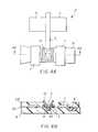
- Figs. 4A-4B to which it is now made referenceillustrate the floating diffusion structure according to the invention.
- the floating diffusion structure obtained according to the inventionis basically of the same type as the one described in reference to the prior art; the following description will emphasize the unique features of the structure according to the invention.
- Charges generated in the solid state image sensor(not shown) are transferred from CCD shift registers (for example) by means of an output gate 1, onto a integrated capacitor formed of a floating diffusion structure 2.
- the floating diffusion structureis comprised of a floating diffusion region 9 connected to the gate electrode 3 of a MOS transistor, which is part of an output amplifier.
- Such a transistorcomprises a drain region 4 and a source region 5. The transfer of charges from the drain region to the source region is controlled by the potential which is applied to the gate electrode 3.
- a reset gate 7is used to reset the floating diffusion to a reference potential at a predetermined time after each pixel sample charge has been deposited in the floating diffusion, a reset drain 8 being provided to this end.
- the floating diffusion structureis comprised of a floating diffusion region 9, the edges of which, as shown in Fig. 4B are self-aligned with the edges of an opening created in the gate electrode 3. As it will be discussed in more detail hereafter, this floating diffusion region is produced by implanting dopant through an opening formed in the gate electrode, thus producing a self-alignment of the floating diffusion region with the edges of the opening in the gate electrode.
- a metallization interconnect 10is applied on the floating diffusion structure to create an ohmic contact between the floating diffusion region and the gate electrode. Since the gate electrode of the MOS transistor forms the interconnect to the floating diffusion region, the area of the interconnect is drastically reduced compared to the floating diffusion structure discussed heretofore. Consequently, the capacitance resulting from this interconnection is also drastically reduced. Furthermore, due to the self-alignment of the floating diffusion region with the edges of the opening made in the gate electrode, a minimum size floating diffusion region is obtained. Accordingly, the capacitance associated with the floating diffusion region itself is reduced.
- Figs. 5A-5Fillustrate the steps of a preferred embodiment of the method according to the invention.
- a gate oxide 30is grown on a substrate of a given conductivity type.
- a substrateis a p-type substrate.
- a polysilicon layer(or other appropriate material) is formed on the gate oxide and, by means of a photoresist, the polysilicon layer is patterned and etched so as to form a gate electrode for the MOS transistor 12.
- the gate electrodeis patterned so that an opening 45 is formed through it.
- the output gate electrode 1 of the solid state image sensor as well as the reset gate electrode 7are also formed.
- the gate electrodes for the other levelsare formed during subsequent patterning and etching steps.
- the floating diffusion region 9is formed by introducing into the substrate a dopant of a conductivity type opposite to the one of the substrate.
- a dopant of a conductivity type opposite to the one of the substrateFor example, for a p-type substrate, a n + -type dopant is used.
- Various techniquescan be used for forming this region, such as, implanting or diffusion.
- One advantage of forming this region through an opening in the gate electrodelies in the fact that the floating diffusion region is self-aligned with the inner edges of the opening, thus limiting the size and capacitance of the floating diffusion region.
- the same dopantis used during this step for forming the reset drain region 8.
- Other regions, such as the source/drain region (not shown) of the MOS transistor as well as other source/drain regions on the solid state image sensorcan be implanted during this step.
- a dielectric 37is deposited, patterned (photoresist 42) and etched to form contacts 39.
- an ohmic contactis formed between the floating diffusion region and the gate electrode.
- This contactcan be formed by metallization interconnect 10, such as aluminum.
- metallizationis also deposited, patterned and etched for other contacts 40 of the image sensor.
Landscapes
- Solid State Image Pick-Up Elements (AREA)
Description
- The invention relates to solid state image-sensors,and particularly to low capacitance floatingdiffusion structures in such a solid state imagesensors.
- Solid state imager sensors operate byconverting incident optical energy into charge that isspatially correlated to the incident optical image. Inorder to reconstruct and/or store the image in anothermedium, the photo-charge is typically converted into avoltage. As illustrated in Figs. 1A-1B, this isusually accomplished by transferring the photo-chargesfrom a storage region by means of an
output gate 1, ofa CCD image sensor for example, onto an integratedcapacitor realized by a floating diffusion. Afloatingdiffusion region 9 is connected to agate electrode 3of a MOS transistor which is part of the outputamplifier. The MOS transistor also comprises asourceregion 4 and adrain region 5. During operation of animage sensor having parallel channels, charge samplesare transferred to thefloating diffusion region 9,which is electrically coupled to thegate electrode 3of the MOS transistor. The voltage on the gateelectrode of the output transistor is the input voltageto the output amplifier and is determined by the pixelcharge transferred onto the floating diffusion. Inorder to prevent the voltage at thegate electrode 3 ofthe MOS transistor from being influenced by pixelcharge samples that have previously been applied to thefloating diffusion, areset gate 7 is used to reset thefloating diffusion to a reference potential determinedby thereset drain 8 at a predetermined time after each pixel sample charge has been deposited on the floatingdiffusion. Each pixel charge is converted to a voltageby the relationship, V=Q/C; where V is voltage, Q ischarge; and C is the capacitance of the floatingdiffusion. - In any application where light levels areinherently or preferably low, (such as copiers), it isdesirable to make this capacitance as small as possibleso that the sensitivity, defined as dV/dQ, is largehence providing an adequate output voltage swing withlower illumination levels. The
floating diffusionstructure 2 is typically formed by ashallow implant 9and contacted viametallization 10 that connects thefloating diffusion region 9 to thegate electrode 3 ofthe MOS transistor, which is part of an amplifier.Such a system is described for example in U.S. PatentNo. 4,594,604 issued to Kub on June 10, 1986. The netcapacitance of such a floating diffusion is determinedby the capacitance between theoutput gate electrode 1of the associated solid state imager and thefloatingdiffusion region 9, the capacitance between theresetgate electrode 7 and thefloating diffusion region 9,the input capacitance of the amplifier, the parasiticcapacitance associated with themetallizationinterconnect 10 and the connection to the MOStransistor gate electrode, and the junction capacitanceof thefloating diffusion region 9. - With such conventional systems, the parasiticcapacitance is increased by the fact that thismetallization interconnect 10 should be long enough topermit a connection with the transistor out of the
active channel region 12 of the transistor (connectionpad 11). In addition, the floating diffusion region isnot the minimum geometry realizable due to the contact and interconnect scheme, hence the minimum junctioncapacitance is limited by the contact patterningresolution and the overlap required for alignmenttolerances. - One method to minimize the net nodecapacitance of the floating diffusion was presented byK. Miwada et al "A 100 MHz Data Rate, 5000-Element CCDLinear Image Sensor With Reset Pulse Level AdjustmentCircuit" IEEE International Solid-State CircuitsConference, Technical Digest, pp 168-169, 275, 1992.According to this approach, as illustrated in Figs. 2A-2Bof the drawings, the
gate electrode 3 of thetransistor is directly connected to thefloatingdiffusion region 9 through a "buried contact". Onepossible process used to produce such a floatingdiffusion structure is illustrated in Figs. 3A-3G ofthe drawings. In Fig. 3A, agate oxide 30 is grown onasubstrate 31 of a given conductivity type. In Fig.3B, a buriedcontact 32 is patterned withphotoresist 33 and etched. In Fig. 3C, afloating diffusion region 9 of a conductivity type opposite to the one of thesubstrate 31 is implanted or diffused. In Fig. 3D, agate electrode 3 is deposited, patterned with aphotoresist 34 and etched, thegate electrode 3 beingin direct contact with thefloating diffusion region 9.Also, during this step, thereset gate electrode 7 aswell as theoutput gate electrode 1 of the image sensorcan be formed. In Fig. 3E, thereset drain region 8 ispatterned (photoresist 36) and implanted with animplant of the same conductivity type as the one of thefloating diffusion region 9. During this implantingstep the source/drain regions (not shown) of the MOStransistor are also implanted. In Fig. 3F, adielectric 37 is deposited, patterned (photoresist 38)and etched to formcontacts 39. In Fig. 3G,metallization 40 is deposited, patterned and etched for the above mentioned contacts. Even if such an approacheliminates the need for any metal interconnect betweenthefloating diffusion 2 and thegate 3 of the MOSamplifier, it has some disadvantages. First itrequires the addition of an extra mask and lithographysequence to the baseline image sensor process, i.e. tothe standard single, double or more, level poly imagerprocess. It also requires either direct contact of thegate oxide 30 withphotoresist 33, or additionalprocess steps to prevent direct contact. As a result,the yield and cost of the device is adversely affected. - EP-A-0 127 223 relates to a semiconductor device which is of particularimportance for CCD sensors. Said device provides compact constructionof channel surface MOS source follower in a p-pocket in an n-type substrate.The source is connected to the p-pocket in order to avoid feedback.The drain is connected to the substrate which acts as a supply line.
- In accordance with the present invention a method producing a lowcapacitance floating diffusion structure of a solid state image sensor asclaimed in
claim 1 and a floating diffusion structure as claimed inclaim 6are provided. Preferred embodiments of the invention are disclosed in thedependent claims. - Accordingly, it is an object of the presentinvention to provide an improved low capacitancefloating diffusion structure in a solid state imagesensor that overcomes the problems mentioned in theabove discussion with respect to conventional methods.
- This object is achieved by providing a methodfor producing a low capacitance floating diffusionstructure of a solid state image sensor having anoutput amplifier provided with a gate electrode,comprising the steps of:
- (a) growing a gate oxide on a substrate of agiven conductivity type;
- (b) forming the gate electrode for the outputamplifier on the gate oxide and patterning the gateelectrode so as to create an opening through it;
- (c) introducing through the opening a dopantof a conductivity type opposite to the givenconductivity type so as to create a floating diffusionregion in the substrate; and
- (d) creating an ohmic contact between thefloating diffusion region and the gate electrode.
- This object is also achieved, in a solidstate image sensor having an output amplifier having agate electrode provided on a substrate of a givenconductivity type, a floating diffusion structurecomprising:
- (a) a floating diffusion region in thesubstrate, the floating diffusion region being of aconductivity type opposite to the given conductivityand being self-aligned with the inner edges of anopening realized in the gate electrode; and
- (b) means for creating an ohmic contactbetween the floating diffusion region and the gateelectrode.
- The following are advantages of the presentinvention: a low capacitance floating diffusionstructure is created without changing or adding stepsto the baseline image sensor fabrication process; andthe parasitic capacitance associated with theinterconnect between the floating diffusion and theelectrode is reduced and the size and capacitance ofthe floating diffusion is reduced.
- FIGS. 1A-1B illustrate a floating diffusionstructure as known in the PRIOR ART;
- FIGS. 2A-2B illustrate another floatingdiffusion structure of the PRIOR ART;
- FIGS. 3A-3G illustrate the prior art steps ofthe process used to produce the floating diffusionstructure of Figs. 2A-2B;
- FIGS. 4A-4B show the floating diffusionstructure of the invention; and
- FIGS. 5A-5F illustrate the steps of themethod according to the invention.
- Figs. 4A-4B to which it is now made referenceillustrate the floating diffusion structure accordingto the invention. The floating diffusion structureobtained according to the invention is basically of thesame type as the one described in reference to theprior art; the following description will emphasize theunique features of the structure according to theinvention. Charges generated in the solid state imagesensor (not shown) are transferred from CCD shiftregisters (for example) by means of an
output gate 1,onto a integrated capacitor formed of a floatingdiffusion structure 2. The floating diffusionstructure is comprised of a floatingdiffusion region 9connected to thegate electrode 3 of a MOS transistor,which is part of an output amplifier. Such atransistor comprises adrain region 4 and asourceregion 5. The transfer of charges from the drainregion to the source region is controlled by thepotential which is applied to thegate electrode 3. Inorder to prevent the voltage at thegate electrode 3 ofthe output transistor from being influenced by pixelcharge samples that have previously been applied to thefloating diffusion, areset gate 7 is used to reset thefloating diffusion to a reference potential at apredetermined time after each pixel sample charge hasbeen deposited in the floating diffusion, areset drain 8 being provided to this end. The floating diffusionstructure is comprised of a floatingdiffusion region 9, the edges of which, as shown in Fig. 4B are self-alignedwith the edges of an opening created in thegate electrode 3. As it will be discussed in moredetail hereafter, this floating diffusion region isproduced by implanting dopant through an opening formedin the gate electrode, thus producing a self-alignmentof the floating diffusion region with the edges of the opening in the gate electrode. Ametallizationinterconnect 10 is applied on the floating diffusionstructure to create an ohmic contact between thefloating diffusion region and the gate electrode.Since the gate electrode of the MOS transistor formsthe interconnect to the floating diffusion region, thearea of the interconnect is drastically reducedcompared to the floating diffusion structure discussedheretofore. Consequently, the capacitance resultingfrom this interconnection is also drastically reduced.Furthermore, due to the self-alignment of the floatingdiffusion region with the edges of the opening made inthe gate electrode, a minimum size floating diffusionregion is obtained. Accordingly, the capacitanceassociated with the floating diffusion region itself isreduced. - Figs. 5A-5F illustrate the steps of apreferred embodiment of the method according to theinvention.
- In Fig. 5A, a
gate oxide 30 is grown on asubstrate of a given conductivity type. Advantageouslysuch a substrate is a p-type substrate. - In Figs. 5B-5C, a polysilicon layer (or otherappropriate material) is formed on the gate oxide and,by means of a photoresist, the polysilicon layer ispatterned and etched so as to form a gate electrode forthe
MOS transistor 12. As it appears from Fig. 5C, thegate electrode is patterned so that anopening 45 isformed through it. During this patterning step, theoutput gate electrode 1 of the solid state image sensoras well as thereset gate electrode 7 are also formed.Typically there can be one, two or three levels of gateelectrodes in a solid state image sensor, and, even ifnot shown, all the gate electrodes of a given level ofthe solid state image sensor are preferably formed during this patterning step. The gate electrodes forthe other levels are formed during subsequentpatterning and etching steps. - In Fig. 5D, the floating
diffusion region 9is formed by introducing into the substrate a dopant ofa conductivity type opposite to the one of thesubstrate. For example, for a p-type substrate, a n+-typedopant is used. Various techniques can be usedfor forming this region, such as, implanting ordiffusion. One advantage of forming this regionthrough an opening in the gate electrode lies in thefact that the floating diffusion region is self-alignedwith the inner edges of the opening, thus limiting thesize and capacitance of the floating diffusion region.As shown in Fig. 5D, the same dopant is used duringthis step for forming thereset drain region 8. Otherregions, such as the source/drain region (not shown) ofthe MOS transistor as well as other source/drainregions on the solid state image sensor can beimplanted during this step. - In Fig. 5E, a dielectric 37 is deposited,patterned (photoresist 42) and etched to form
contacts 39. - In Fig. 5F, an ohmic contact is formedbetween the floating diffusion region and the gateelectrode. This contact can be formed by
metallizationinterconnect 10, such as aluminum. During this step,metallization is also deposited, patterned and etchedforother contacts 40 of the image sensor. - From the above description, it should beclear that such a method does not add any furtherprocess steps to the standard single or double levelpoly imager process. This is not the case of theapproach described by Miwada et al, in which extramasking and implanting steps are required.
Claims (8)
- A method producing a low capacitancefloating diffusion structure of a solid state imagesensor having an output amplifier provided with a gateelectrode (3), comprising the steps of:(a) growing a gate oxide (30) on a substrate (31) of agiven conductivity type;(b) forming said gate electrode (3) for saidoutput amplifier on said gate oxide (30) and patterning saidgate electrode (3) so as to create an opening through it;(c) introducing through said opening adopant of a conductivity type opposite to said givenconductivity type so as to create a floating diffusionregion (9) in said substrate (31); and(d) creating an ohmic contact between saidfloating diffusion region (9) and said gate electrode (3).
- A method according to claim 1 whereinsaid floating diffusion region (9) is formed by implantingsaid opposite conductivity type dopant into saidsubstrate (31).
- A method according to claim 1 whereinsaid floating diffusion region (9) is formed by diffusion.
- A method according to claim 1 whereinsaid ohmic contact is created by metallization.
- A method according to claim 1 whereinother regions of the image sensor are doped with adopant of said opposite conductivity type during step(c).
- A floating diffusion structure (2) in a solid state image sensor having anoutput amplifier, said output amplifier having a gateelectrode provided (3) on a gate oxide (30) on a substrate (31) of a givenconductivity type, said floating diffusion structure (2)comprising:(a) a floating diffusion region (9) in saidsubstrate (31), said floating diffusion region (9) being of aconductivity type opposite to said given conductivityand the edges of which being self-aligned with the inner edges of anopening realized in said gate electrode (3) and said gate oxide (30); and(b) means for creating an ohmic contactbetween said floating diffusion region (9) and said gateelectrode (3).
- A floating diffusion structure (2)according to claim 6 wherein said substrate (31) is ap-type substrate.
- A floating diffusion structure (2) accordingto claim 7 wherein said floating diffusion region (9) is an+-type region.
Applications Claiming Priority (2)
| Application Number | Priority Date | Filing Date | Title |
|---|---|---|---|
| US188500 | 1994-01-26 | ||
| US08/188,500US5387536A (en) | 1994-01-26 | 1994-01-26 | Method of making a low capacitance floating diffusion structure for a solid state image sensor |
Publications (3)
| Publication Number | Publication Date |
|---|---|
| EP0665598A2 EP0665598A2 (en) | 1995-08-02 |
| EP0665598A3 EP0665598A3 (en) | 1995-09-13 |
| EP0665598B1true EP0665598B1 (en) | 1999-06-23 |
Family
ID=22693413
Family Applications (1)
| Application Number | Title | Priority Date | Filing Date |
|---|---|---|---|
| EP95200089AExpired - LifetimeEP0665598B1 (en) | 1994-01-26 | 1995-01-14 | Low capacitance floating diffusion structure for a solid state image sensor |
Country Status (4)
| Country | Link |
|---|---|
| US (2) | US5387536A (en) |
| EP (1) | EP0665598B1 (en) |
| JP (1) | JP3842826B2 (en) |
| DE (1) | DE69510384T2 (en) |
Families Citing this family (13)
| Publication number | Priority date | Publication date | Assignee | Title |
|---|---|---|---|---|
| JPH07115184A (en)* | 1993-08-24 | 1995-05-02 | Canon Inc | Stacked solid-state imaging device and manufacturing method thereof |
| US5591997A (en)* | 1995-01-17 | 1997-01-07 | Eastman Kodak Company | Low capacitance floating diffusion structure for a solid state image sensor |
| KR100223826B1 (en)* | 1997-06-04 | 1999-10-15 | 구본준 | Manufacturing method of CCD image device |
| FR2781929B1 (en)* | 1998-07-28 | 2002-08-30 | St Microelectronics Sa | IMAGE SENSOR WITH PHOTODIODE ARRAY |
| JP2002118249A (en)* | 2000-10-06 | 2002-04-19 | Sony Corp | Solid-state image pick up element |
| FR2820882B1 (en) | 2001-02-12 | 2003-06-13 | St Microelectronics Sa | THREE TRANSISTOR PHOTODETECTOR |
| FR2820883B1 (en) | 2001-02-12 | 2003-06-13 | St Microelectronics Sa | HIGH CAPACITY PHOTODIODE |
| FR2824665B1 (en)* | 2001-05-09 | 2004-07-23 | St Microelectronics Sa | CMOS TYPE PHOTODETECTOR |
| JP4004891B2 (en)* | 2002-08-19 | 2007-11-07 | 富士フイルム株式会社 | CCD type solid-state imaging device |
| JP4354315B2 (en) | 2004-03-22 | 2009-10-28 | 東芝機械株式会社 | Aluminum melt contact member and method of manufacturing the same |
| JP4752447B2 (en)* | 2005-10-21 | 2011-08-17 | ソニー株式会社 | Solid-state imaging device and camera |
| JP5132102B2 (en)* | 2006-08-01 | 2013-01-30 | キヤノン株式会社 | Photoelectric conversion device and imaging system using photoelectric conversion device |
| JP5305622B2 (en)* | 2006-08-31 | 2013-10-02 | キヤノン株式会社 | Method for manufacturing photoelectric conversion device |
Family Cites Families (8)
| Publication number | Priority date | Publication date | Assignee | Title |
|---|---|---|---|---|
| FR2533371B1 (en)* | 1982-09-21 | 1985-12-13 | Thomson Csf | GRID STRUCTURE FOR AN INTEGRATED CIRCUIT COMPRISING ELEMENTS OF THE GRID-INSULATOR-SEMICONDUCTOR TYPE AND METHOD FOR PRODUCING AN INTEGRATED CIRCUIT USING SUCH A STRUCTURE |
| NL8301629A (en)* | 1983-05-09 | 1984-12-03 | Philips Nv | SEMICONDUCTOR DEVICE. |
| US4594604A (en)* | 1983-10-21 | 1986-06-10 | Westinghouse Electric Corp. | Charge coupled device with structures for forward scuppering to reduce noise |
| JPH079981B2 (en)* | 1985-02-05 | 1995-02-01 | ソニー株式会社 | Charge transfer device |
| US4892842A (en)* | 1987-10-29 | 1990-01-09 | Tektronix, Inc. | Method of treating an integrated circuit |
| US5288651A (en)* | 1989-11-09 | 1994-02-22 | Kabushiki Kaisha Toshiba | Method of making semiconductor integrated circuit device including bipolar transistors, MOS FETs and CCD |
| US5151380A (en)* | 1991-08-19 | 1992-09-29 | Texas Instruments Incorporated | Method of making top buss virtual phase frame interline transfer CCD image sensor |
| US5341008A (en)* | 1993-09-21 | 1994-08-23 | Texas Instruments Incorporated | Bulk charge modulated device photocell with lateral charge drain |
- 1994
- 1994-01-26USUS08/188,500patent/US5387536A/ennot_activeExpired - Lifetime
- 1995
- 1995-01-14DEDE69510384Tpatent/DE69510384T2/ennot_activeExpired - Lifetime
- 1995-01-14EPEP95200089Apatent/EP0665598B1/ennot_activeExpired - Lifetime
- 1995-01-25JPJP00985895Apatent/JP3842826B2/ennot_activeExpired - Lifetime
- 1996
- 1996-06-27USUS08/675,328patent/US5621230A/ennot_activeExpired - Lifetime
Also Published As
| Publication number | Publication date |
|---|---|
| US5387536A (en) | 1995-02-07 |
| EP0665598A2 (en) | 1995-08-02 |
| DE69510384D1 (en) | 1999-07-29 |
| DE69510384T2 (en) | 2000-01-13 |
| JP3842826B2 (en) | 2006-11-08 |
| US5621230A (en) | 1997-04-15 |
| JPH07263662A (en) | 1995-10-13 |
| EP0665598A3 (en) | 1995-09-13 |
Similar Documents
| Publication | Publication Date | Title |
|---|---|---|
| US5192990A (en) | Output circuit for image sensor | |
| US8003506B2 (en) | Single poly CMOS imager | |
| US7687832B2 (en) | Method of fabricating a storage gate pixel design | |
| US7517714B2 (en) | Image sensors for reducing dark current and methods of fabricating the same | |
| US6835637B2 (en) | Multi-layered gate for a CMOS imager | |
| US7279672B2 (en) | Image sensor having pinned floating diffusion diode | |
| US8802472B2 (en) | Small pixel for image sensors with JFET and vertically integrated reset diode | |
| EP0665598B1 (en) | Low capacitance floating diffusion structure for a solid state image sensor | |
| US20030160295A1 (en) | Semiconductor device, image pickup device using the same, and photoelectric conversion device | |
| US7230289B2 (en) | Solid-state imaging device and method of manufacturing the same | |
| US5712498A (en) | Charge modulation device | |
| US5591997A (en) | Low capacitance floating diffusion structure for a solid state image sensor | |
| US4677453A (en) | Solid state image sensor | |
| US7652343B2 (en) | Solid-state imaging device and method for manufacturing same | |
| KR20050038034A (en) | Image sensor, camera system comprising the image sensor and method of manufacturing such a device | |
| EP0282557B1 (en) | Output circuit for image sensor | |
| US5491354A (en) | Floating gate charge detection node | |
| US6111281A (en) | Solid-state image-pickup device and MOS transistor having a reduced incidental capacitance | |
| US5804844A (en) | Solid-state imager with container LOD implant | |
| KR100657142B1 (en) | Contact structure for pixel shrink of image sensor and manufacturing method | |
| KR20060129588A (en) | Image sensor and manufacturing method thereof | |
| JPS61123171A (en) | Solid-state image pickup device |
Legal Events
| Date | Code | Title | Description |
|---|---|---|---|
| PUAI | Public reference made under article 153(3) epc to a published international application that has entered the european phase | Free format text:ORIGINAL CODE: 0009012 | |
| PUAL | Search report despatched | Free format text:ORIGINAL CODE: 0009013 | |
| AK | Designated contracting states | Kind code of ref document:A2 Designated state(s):DE FR GB | |
| AK | Designated contracting states | Kind code of ref document:A3 Designated state(s):DE FR GB | |
| 17P | Request for examination filed | Effective date:19960308 | |
| 17Q | First examination report despatched | Effective date:19961223 | |
| GRAG | Despatch of communication of intention to grant | Free format text:ORIGINAL CODE: EPIDOS AGRA | |
| GRAG | Despatch of communication of intention to grant | Free format text:ORIGINAL CODE: EPIDOS AGRA | |
| GRAG | Despatch of communication of intention to grant | Free format text:ORIGINAL CODE: EPIDOS AGRA | |
| GRAH | Despatch of communication of intention to grant a patent | Free format text:ORIGINAL CODE: EPIDOS IGRA | |
| GRAH | Despatch of communication of intention to grant a patent | Free format text:ORIGINAL CODE: EPIDOS IGRA | |
| GRAA | (expected) grant | Free format text:ORIGINAL CODE: 0009210 | |
| AK | Designated contracting states | Kind code of ref document:B1 Designated state(s):DE FR GB | |
| REF | Corresponds to: | Ref document number:69510384 Country of ref document:DE Date of ref document:19990729 | |
| ET | Fr: translation filed | ||
| PLBE | No opposition filed within time limit | Free format text:ORIGINAL CODE: 0009261 | |
| 26N | No opposition filed | ||
| REG | Reference to a national code | Ref country code:GB Ref legal event code:IF02 | |
| REG | Reference to a national code | Ref country code:GB Ref legal event code:732E Free format text:REGISTERED BETWEEN 20110704 AND 20110706 | |
| REG | Reference to a national code | Ref country code:FR Ref legal event code:TP Owner name:OMNI VISION TECHNOLOGIES, INC., US Effective date:20110829 | |
| PGFP | Annual fee paid to national office [announced via postgrant information from national office to epo] | Ref country code:GB Payment date:20131227 Year of fee payment:20 | |
| PGFP | Annual fee paid to national office [announced via postgrant information from national office to epo] | Ref country code:DE Payment date:20140131 Year of fee payment:20 | |
| PGFP | Annual fee paid to national office [announced via postgrant information from national office to epo] | Ref country code:FR Payment date:20131223 Year of fee payment:20 | |
| REG | Reference to a national code | Ref country code:DE Ref legal event code:R071 Ref document number:69510384 Country of ref document:DE | |
| REG | Reference to a national code | Ref country code:GB Ref legal event code:PE20 Expiry date:20150113 | |
| PG25 | Lapsed in a contracting state [announced via postgrant information from national office to epo] | Ref country code:GB Free format text:LAPSE BECAUSE OF EXPIRATION OF PROTECTION Effective date:20150113 |