EP0652415B1 - A device for measuring the thickness of thin films - Google Patents
A device for measuring the thickness of thin filmsDownload PDFInfo
- Publication number
- EP0652415B1 EP0652415B1EP94307593AEP94307593AEP0652415B1EP 0652415 B1EP0652415 B1EP 0652415B1EP 94307593 AEP94307593 AEP 94307593AEP 94307593 AEP94307593 AEP 94307593AEP 0652415 B1EP0652415 B1EP 0652415B1
- Authority
- EP
- European Patent Office
- Prior art keywords
- light beam
- sample
- axis
- input
- angle
- Prior art date
- Legal status (The legal status is an assumption and is not a legal conclusion. Google has not performed a legal analysis and makes no representation as to the accuracy of the status listed.)
- Expired - Lifetime
Links
- 239000010409thin filmSubstances0.000titleclaims3
- 230000001427coherent effectEffects0.000claims5
- 238000003384imaging methodMethods0.000claims4
- 239000011521glassSubstances0.000claims2
- 230000003287optical effectEffects0.000claims2
Images


Classifications
- G—PHYSICS
- G01—MEASURING; TESTING
- G01B—MEASURING LENGTH, THICKNESS OR SIMILAR LINEAR DIMENSIONS; MEASURING ANGLES; MEASURING AREAS; MEASURING IRREGULARITIES OF SURFACES OR CONTOURS
- G01B11/00—Measuring arrangements characterised by the use of optical techniques
- G01B11/02—Measuring arrangements characterised by the use of optical techniques for measuring length, width or thickness
- G01B11/06—Measuring arrangements characterised by the use of optical techniques for measuring length, width or thickness for measuring thickness ; e.g. of sheet material
- G01B11/0616—Measuring arrangements characterised by the use of optical techniques for measuring length, width or thickness for measuring thickness ; e.g. of sheet material of coating
- G01B11/0641—Measuring arrangements characterised by the use of optical techniques for measuring length, width or thickness for measuring thickness ; e.g. of sheet material of coating with measurement of polarization
- G01B11/065—Measuring arrangements characterised by the use of optical techniques for measuring length, width or thickness for measuring thickness ; e.g. of sheet material of coating with measurement of polarization using one or more discrete wavelengths
Definitions
- the present inventionrelates to systems and methods for non-destructive quality control in general and to optical systems and methods for measuring the thickness and index of refraction of thin films, in particular.
- Optical measuring instrumentsare typically utilized in the microelectronic industry for non-contact, non-destructive measurement of the thickness of thin films.
- Two main systemsare utilized, spectrophotometers (or reflectometers) and ellipsometers.
- spectrophotometersor reflectometers
- ellipsometersThe following U.S. Patents represent the prior art:
- Coates et aldescribe a system for measuring thin film thicknesses by directing a plane polarized laser light beam to the film at the Brewster angle of the substrate and by measuring the intensity changes between a measurement from the substrate alone and from the film coated substrate.
- EP 558781A1describes a method an apparatus for exposure of substrates which uses a one-dimensional translation apparatus to translate the optical head.
- the two prior art systemsare illustrated as Figs 1A and 1B, respectively, to which reference is now made.
- the spectrophotometerutilizes the fact that light beams reflected off thin film boundaries, will interfere one with another.
- the spectrophotometer of Fig 1Ameasures the reflectance of selected points of a sample 10 as a function of the light wavelength, usually in the visible of near UV spectral ranges.
- Computer analysis of the detected spectral reflection functionespecially its minima and maxima, provides the thickness, and in some cases, also the index of refraction of the measured film.
- the spectrophotometertypically includes a transmitter 12 with a light source and appropriate optics, a beam splitter 14, an objective lens 16, a tube lens 18 and a receiver 20 which includes optical and electronic means for measurement of light intensity as a function of the input light wavelength.
- the transmitter 12produces a collimated light beam 22 which is deflected by the beam splitter 14 and focused on the sample 10 by the objective lens 16.
- the reflected beam, labeled 24,is collected by the microscope imaging optics (lenses 16 and 18) on a spectroscopic measurement unit within the receiver 20.
- sample 10is placed on an x-y stage 26.
- X-Y stage 26is typically very precise and heavy and, as a result, moves very slowly.
- the spectrophotometershave difficulty measuring structures with very small reflectance, such as thin films on glass substrates, because the relatively low brightness of traditional white light sources does not provide a sufficient signal-to-noise ratio (SNR).
- Spectrophotometersalso have difficulty measuring films with unknown or unrepeatable dispersions of optical constants, such as amorphous silicon.
- the spectral photometry methodis at present widely used in industry because the instrumentation for this method is easily combined with optical microscopes and can utilize conventional microscope optics.
- Ellipsometersmeasure changes in the polarization of light caused by reflectance from the test surface. These changes, characterized as amplitude and phase changes, are very sensitive to the thickness and optical properties of thin films.
- FIG. 1BA prior art ellipsometer is illustrated in Fig. 1B. It includes a transmitter 30 which includes a light source and appropriate optics, a polarizer 32, an optional compensator (phase retarder) 34, an analyzer 36 and a receiver 38 with a photo-detector and appropriate electronics.
- the polarizer 32polarizes the light beam 40 produced by light source 30.
- the reflected light beam, labeled 42passes through the analyzer 36 before reaching the receiver 38.
- the compensator 34it may be located either between the polarizer 32 and the test sample 10 or between the sample 10 and the analyzer 36.
- the ellipsometric methodrequires oblique illumination, i.e. an angle of incidence ⁇ between an incident light beam 40 and a normal 44 to the sample 10 must be greater than zero.
- the angle between a reflected light beam 42 and the normal 44is equal to the angle of incidence ⁇ .
- the angle of incidence ⁇should be close to the Brewster angle ⁇ B of the substrate. In practice, the angle of incidence ⁇ ranges from 45° to 70°.
- ellipsometersmeasure two polarization parameters (amplitude and phase), both of which are independent of the light intensity, they are quite accurate and can also measure ultra thin films of the size of 0 - 100 ⁇ . However, since ellipsometers require oblique illumination as well as a highly collimated light beam, their use for high spatial resolution measurements in dense patterned structures is rather difficult.
- Null-ellipsometersprovide the most accurate thickness measurements but they require at least several seconds per measuring point.
- Rotating-analyzer ellipsometersprovide very high speed measurements (portions of a second per measuring point), but their sensitivity and accuracy are usually less than those of null-ellipsometers.
- the opto-mechanical apparatusis complicated, large and heavy, and thus, the x-y stage 26 is translated between measurement points, coming to a complete stop before measurement begins.
- the time between measurementsdepends on the mass of the x-y stage 26 and on the positioning accuracy requirements and may take at least several seconds (sometimes up to several tens of seconds). This limits the speed with which a thickness mapping can occur, especially during inspection of large size substrates such as 8" VLSI silicon wafers, 18"x18" LCD glass panels, etc.
- the footprint, or space on the floor which each machine utilizes,is typically at least twice the size of the x-y stage 26 due to its translation.
- the prior art measuring devicesare utilized for measuring once a deposition process has been completed. They cannot be utilized for in-process control, since wafer handling and other mechanical movements are not allowed within a vacuum chamber.
- the apparatusincludes a beam deflector for deflecting a light beam to and from the surface while maintaining a predetermined angle of incidence and reflection.
- a device for measuring the thickness of thin films on a samplewhich includes a) an illuminator for providing a collimated input light beam along an input axis, b) a receiver for receiving a collimated output light beam along an output axis parallel to the input axis, and c) a beam deflector, translatable at least along a scanning axis parallel to the input axis, for directing the input light beam towards the sample and the output light beam from the sample towards the receiver.
- the receiverincludes a lens and a diaphragm having a pinhole which is located at a focal point of the lens.
- the beam deflectorcan be one- or two-dimensional.
- the beam deflectorincludes a) a first beam deflecting element which deflects the input light beam towards the sample, b) a second beam deflecting element which deflects a light beam reflected from the sample along the output axis, and c) an objective lens which collimates the reflected beam.
- the collimated beamis the output light beam.
- the beam deflectortranslates along the scanning axis and along a second scanning axis perpendicular to the third axis.
- the beam deflectorpreferably includes four mirrors and an objective lens.
- the first mirrordeflects the input light beam from the input axis to the second scanning axis.
- the second mirrordeflects the input light beam from the second scanning axis to the sample.
- the third mirrordeflects a reflected light beam from the sample to the second scanning axis.
- the fourth mirrorfor deflecting the reflected light beam from the second scanning axis to the output axis.
- the objective lensis operative to collimate the reflected beam.
- the deviceis an ellipsometer.
- the receiveradditionally includes an analyzer and a photodetector and the first and second beam deflecting elements are mirrors.
- the illuminatorincludes a light source and a polarizer. The illuminator or the receiver can optionally include a compensator.
- the deviceis a spectrophotometer.
- the receiveradditionally includes a spectrophotometric detector, the first beam deflecting element is a beam splitter and the second beam deflecting element is a mirror.
- the beam deflectoradditionally comprises a lens for focusing the input light beam on the sample after deflection by the beam splitter.
- the apparatus of the present inventionmay be incorporated within equipment, such as cluster tools, for film deposition.
- the deviceincludes a) an illuminating unit for providing a collimated input light beam along an input axis, b) a receiver for receiving a collimated output light beam along an output axis parallel to the input axis and c) a beam deflector, translatable at least along a scanning axis parallel to the input axis, for directing the input light beam towards the sample and the output light beam from the sample towards the receiver.
- the input light beamis preferably formed of at least one of coherent and incoherent light and impinges on the sample at a desired angle of incidence.
- the receiverincludes a) a first imaging lens, b) a grating located at a focal point of the first imaging lens at an angle to an axis of the output light beam equivalent to the angle of incidence, the grating having a pinhole located on the axis of the output light beam, c) at least one photodetector for detecting generally coherent light received through the pinhole, d) a second imaging lens and e) a camera for receiving incoherent light from the area to be measured as deflected by the grating and as imaged by the second imaging lens.
- the deviceincludes apparatus for measuring an actual angle of incidence which may vary from the desired angle of incidence.
- the apparatus for measuringutilizes optical elements forming part of the illuminator and receiver.
- the apparatus for measuringpreferably includes a position sensing device.
- the deviceis incorporated within a cluster tool having a vacuum chamber in which the sample is held.
- the vacuum chamberpreferably includes a cover having glass plates incorporated therein at an angle perpendicular to axes of the beams impinging on and reflecting from the sample.
- the glass platesextend parallel to the scanning axis.
- the deviceincludes a polarizer, analyzer and optional compensator which are generally located close to the sample.
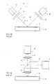
- FIG. 2is a side view and Fig. 3 is a top view.
- the optical measuring deviceis an ellipsometer. This is by way of example only; the principles of the present invention can also be implemented in a spectrophotometer, as illustrated in Fig. 6, described in detail hereinbelow.
- the ellipsometer of Fig. 2typically comprises a stationary illuminator 50, a stationary detector 52, a translating beam deflector 54, and a stationary support 56, such as a stage, ring, etc., for holding a sample 57.
- the illuminator 50typically comprises of elements similar to those of the prior art. Therefore, similar elements have similar reference numerals.
- the illuminator 50typically comprises transmitter 30 which includes a laser light source, a polarizer 32 and an optional compensator (phase retarder) 34.
- the laser light sourcewith its associated optics (not shown), produces a highly collimated laser light beam.
- the beam deflector 54typically comprises two mirrors 72 and 74 and a first objective lens 75.
- Mirror 74deflects a light beam 64, reflected from the sample 57, to a beam 65 along a direction parallel to the X scanning axis.
- First objective lens 75whose focal plane is at the plane of sample 57, typically collimates beam 65, thereby producing a collimated reflected beam 60.
- the beam deflector 54is translated along the X-axis.
- the movement of the beam deflector 54generally does not affect the measurement quality of the ellipsometer since the input and output light beams 58 and 60 are highly collimated and parallel to the scanning axis.
- beam deflector 54only comprises the mirrors 72 and 74 and objective lens 75, it is lightweight and therefore, its translation is fast, on the order of the measurement time.
- the support 56is stationary, therefore, the device of the present invention has a minimal footprint of the size of the sample 57.
- reflection from the mirrors 72 and 74may be not fully specular. Typically, some depolarized scattered light is also produced. While the percentage of scattered light is very small relative to the specular light (1:1000 or even less, depending on the quality of the mirror surface), the scattered light could limit the signal-to-noise ratio (SNR) of the system and thus, limit the measurement accuracy.
- SNRsignal-to-noise ratio
- the detector 52typically comprises scattered light reducing elements in addition to the standard analyzer 36 and receiver 38.
- the scattered light reducing elementstypically are a second objective lens 76 and a diaphragm 77, located at the focal plane of objective lens 76 and having a pinhole 78, and a condenser 79.
- the analyzer 36is typically placed within the collimated light beam 60, between objective lenses 75 and 76. Since pinhole 78 is placed at the center of the image plane which is the focal plane of lens 76, it acts as an aperture stop, allowing only the collimated portion of light beam 60 to pass through. Thus, the pinhole drastically reduces the widely scattered depolarized light introduced by the mirrors. Condenser 79 collects the light from the pinhole 78 and provides it to receiver 38.
- the angular aperture of the detector 52is less than one mrad.
- the resultant intensity of scattered light reaching the detector 38is less than 10 -3 % of the polarized light which is the minimum necessary for accurate ellipsometric measurements.
- Receiver 38typically comprises a photo-detector and appropriate electronics. Although not shown, the detector 52 can also include the compensator 34, located before the analyzer 36.
- the ellipsometer of Fig. 3provides two-dimensional scanning with a two-dimensional scanning unit 80.
- the remaining elementsare similar to those of Fig. 2 and therefore, have similar reference numerals.
- Scanning unit 80typically comprises a beam deflector 82 (see Fig. 2) similar to beam deflector 54, which slides along X-axis rails 84.
- the X-axis rails 84are attached together and to carriages 90, forming an X-axis unit 86 which, in turn, translates along Y-axis rails 88 via the carriages 90.
- Scanning unit 80typically also comprises mirrors 92 and 94 (see Fig. 3) which deflect beams between the X- and Y-axes. Specifically, mirror 92 deflects the input beam 58 from the Y-axis to the X-axis, producing beam 96 which is parallel to the X-axis. Mirror 94 receives beam 98, the output of the beam deflector 82, along the X-axis and deflects it towards the Y-axis, producing thereby reflected beam 60.
- the scattered light reducing elements 76 - 79are efficient for a number of mirrors, as long as none of the mirrors are located very close to either the object or image planes.
- FIG. 4is a partial schematic, partial block-diagram illustration and Figs. 5A - 5C are schematic illustrations of the elements of the monitor of Fig. 4.
- the monitor of Fig. 4is operative to measure the thickness of thin films within deposition equipment such as cluster tools.
- a cluster toolis a large vacuum system which consists of several chambers, each performing a specific deposition process on a single silicon wafer ("single wafer processing"). An internal robot transfers each wafer from chamber to chamber without breaking the vacuum, thus several deposition processes may be carried out before the wafer is removed from the cluster tool.
- the present inventionis typically installed on a cool-down vacuum chamber to which each wafer is brought for one-two minutes after each deposition process. It thus measures the film thickness after each deposition.
- the in-process monitorcomprises a coherent and an incoherent imaging unit and an angle of incidence measuring unit, portions of whose optical paths are identical.
- the coherent imaging unitis utilized for ellipsometric measurements and thus, is similar to that described hereinabove with respect to Fig. 2.
- the incoherent imaging unitis typically operative for pattern recognition.
- the monitorcomprises an illumination unit, labeled 100, a detection unit, labeled 102, a beam deflector, labeled 104, and support 105, similar to support 56.
- two stationary glass plates 112built into a cover 110 of vacuum chamber 108, along the direction of the X-axis, are two stationary glass plates 112 operative to enable the light beam to reach the sample 57 from outside the chamber.
- the planes of their surfacesare located perpendicular to the path of optical beams 59 and 64.
- the glass plates 112are mechanically strong enough to withstand the pressure difference between the vacuum within chamber 108 and the atmospheric pressure outside of it.
- the plates 112are made from stress-free glass of about 5 mm thick and their aspect ratio (width/length) is about 1:50. The resultant induced birefringence is negligible and therefore, the plates generally do not affect the optical measurements.
- Beam deflector 104typically comprises focusing lens 150 and objective lens 152, two mirrors 154 and 156 and X-axis translation apparatus 153 (see Fig. 4), such as a linear motor.
- focusing lens 150focuses the polarized and collimated light beam, labeled 158, onto the surface of sample 57 and the objective lens 152 collimates the divergent beam 64 into the reflected beam, labeled 159.
- lenses 150 and 152are thin, simple lenses made of stress free glass to reduce to zero their birefringence. They may also be located between the mirrors 154 and 156 and the sample 57.
- the two mirrors 154 and 156are similar to mirrors 72 and 74 of Fig. 2 and are operative to direct the light beam to and from the sample 57 at the desired angle of incidence ⁇ in the Y-Z plane and to deflect the light beam between the X- and Y-axes, as shown in Fig. 4.
- the light beam 59always impinges on the sample 57 at the desired angle of incidence ⁇ , even though the beam deflector 104 is translated along the X-axis.
- the illumination unit 100is detailed in Fig. 5B and typically comprises a light source unit 120, a quarter wave plate (QWP) 122, a polarizer 124 and a compensator 126.
- QWPquarter wave plate
- the light source unit 120typically comprises two coherent light sources 130 and 132 for ellipsometric measurements and one incoherent light source 134 and a condenser 136 for incoherent imaging.
- the condenser 136collimates the output of light source 134.
- Illumination unit 100also comprises two beam splitters 138 for combining the light from the three light sources 130, 132 and 134 onto a single path 139.
- Beam-splitters 138typically are dichroic or polarizing. If they are polarizing, the planes of polarization of the two lasers 130 and 132 are set to be orthogonal.
- the two coherent light sources 130 and 132are laser diodes which produce highly monochromatic and collimated light for ellipsometric measurements.
- Laser 130has a wavelength lambda_1 in the visible spectral range, preferably within the range of 630 to 680nm
- laser 132has a wavelength lambda_2 in the near infra-red (IR) spectral range, preferably within the range of 810 to 830nm.
- the visible lightis preferable for measuring such films as silicon dioxide, silicon nitride and other dielectric layers.
- the IR lightis preferable for silicon layers (poly-silicon, amorphous silicon and the like). Under IR light, the silicon layers are almost transparent and their optical parameters are generally repeatable between processes.
- the incoherent light source 134used during pattern recognition, can be any suitable light source, such as a high brightness LED, quartz-tungsten lamp, xenon arc lamp, etc. Its specific range should preferably be narrow, for example of 780 ⁇ 20nm.
- the incoherent light source 134is operative and it, together with the focusing lens 150, the and the condenser 136 form an incoherent illuminator whose light beam forms an incoherent light spot on the surface of sample 57.
- the size and divergence of the incoherent light beammust be sufficient to illuminate the desired field of view, e.g. about 1 mm in its shortest dimension, at any position of the beam deflector 104 along the X-axis.
- the quarter-wave plate (QWP) 122useful for ellipsometric measurements, is oriented with its optical axis at an angle of ⁇ 45° relative to the planes of polarization of the lasers 130 and 132 and transforms their linear polarization to a circular one.
- the QWP 122should be achromatic throughout the utilized spectral range of 630 to 830nm. Suitable achromatic QWPs are manufactured, for example, by Meadowlarc Optics company, USA.
- the polarizer 124 and compensator 126have associated therewith motor drives 140 and 142, respectively.
- motor drives 140 and 142typically operate with precise angular encoders. Since most ellipsometric measurement algorithms do not require rotation of the compensator, a manual driving mechanism (for alignment only) may alternatively be used instead the motor drive 142.
- the polarizer 124is achromatic.
- a suitable polarizeris a Glan-Thomson polarization prism.
- a sheet polarizersuch as the HN38S type from Polaroid Corporation of the USA, is suitable.
- an extinction ratio of more than 10 5is required for reaching the thickness measurement accuracy required in microelectronic deposition process control.
- the detection unit 102typically comprises a two-dimensional image acquisition system (part of the incoherent imaging unit), an ellipsometric detector unit (part of the coherent imaging unit) and an angle of incidence measurement unit.
- the ellipsometric detector unit of detection unit 102is comprised of elements similar to those of the ellipsometer of Fig. 2, but extended to operate with the two wavelengths, lambda_1 and lambda_2.
- the ellipsometric detector unitoperates with the objective lens 152 and typically comprises the analyzer, labeled 160, its associated motor 162, an imaging lens 164, a diaphragm 165 having a pinhole 166, a condenser 168, two independent photo-detectors 170 and 172, two band pass spectral filters 174 and 176 and a beam splitter 178.
- the analyzer 160is similar to polarizer 124 and is therefore, achromatic for the two wavelength configuration.
- the pinhole 166is located at the image plane of the optical imaging system (lenses 152 and 164) which is the focal plane of lens 164, only that portion of the light reflected from the surface of sample 57 which is the size of pinhole 166 will come through pinhole 166.
- Condenser 168collects the light and focusses it onto the photo-detectors 170 and 172.
- the beam splitter 178splits the incoming beam into two beams, each having the appropriate wavelength, lambda_1 and lambda_2.
- the photo-detectors 170 and 172detect, via the filters 174 and 176 respectively, the intensity of light of the two wavelengths lambda_1 and lambda_2, respectively.
- the photo-detectorsare silicon photovoltaic detectors, such as the S5591 manufactured by Hamamatsu Photonics U.U. of Hamamatsu City, Japan. If necessary, more sensitive but more expansive photo-multipliers may be used.
- the present inventionallows simultaneous measurement of two wavelengths which enables the measurement of two pairs of ellipsometric parameters, the amplitude parameter psi and the phase parameter delta.
- four parameters of the thin film structuree.g. thickness and index of refraction of each of two layers, can be simultaneously determined. Such a measurement is useful when two different layers are deposited on the sample 57 in one deposition cycle.
- the spatial resolution of the monitor of the present inventiondepends only on the size of pinhole 166 and on the point spread function of the coherent imaging system.
- the point spread functionis defined by the F-stop of the coherent imaging system and is generally quite small. Practically, the thickness measurements are carried out on scribe lines, pads or special test areas which are not less than 50 ⁇ m wide and therefore, a pinhole size of 20 - 40 ⁇ m and an F# of 5 - 6 is acceptable.
- pinhole 166has to be asymmetrical to compensate.
- the two-dimensional image acquisition systemtypically operates in conjunction with the incoherent image illuminator and utilizes the objective lens 152 located on the beam deflector 104.
- the image acquisition systemtypically comprises the imaging lens 164, the diaphragm 165 with the pinhole 166, a magnifying lens 180, a mirror 182, an optional band pass filter 184 and a high resolution, area charge coupled device (CCD) 186.
- the diaphragm 165is made from a grating 167 which has the pinhole 166 therein.
- the grating 167does not affect the ellipsometric measurements.
- the surfaces of sample 57 and grating 167are respectively located in the focal planes of lenses 152 and 164.
- the lenses 152 and 164typically have the same focal length, thereby providing an optical magnification M of 1X.
- the image planeis also tilted relative to the optical axis (the axis of a beam 188) from the analyzer 160.
- the grating 167tilted by the angle ⁇ relative to axis 188, is the imaging plane for the imaging system of lenses 152 and 164 and is the object plane (or intermediate image plane) for the imaging system of lens 180.
- the object planesample surface
- the image planeis tilted at the same angle ⁇ relative to their optical axes.
- ⁇the angle relative to their optical axes.
- the grating 167is aligned along the intermediate image plane.
- the magnifying lens 180is placed in the direction of the first diffraction maximum for the wavelength lambda_3 of the incoherent illuminator.
- the lens 180provides magnification, of at least 5X, which is strong enough for recognition of the test areas on the wafer.
- the high resolution CCD 186such as the TM-6CN CCD manufactured by Pulnix America Inc. of Sunnyvale, California, USA, transforms the image to a video signal.
- the optional band pass filter 184ensures that only light from the incoherent illuminator is used for imaging.
- the lens 180should be corrected for the chromatic aberrations in the spectral range of the incoherent light.
- the quality of the obtained imagedepends strongly on the F-stops (F#) of the objective and imaging lenses 152 and 164 and the aberrations that they produce.
- F#F-stops
- the F#is about 6, a value which is used for high quality photography and other applications.
- the lens 180is a high quality microscope grade objective lens and therefore, does not significantly affect the final image quality.
- the pinhole 166serves to locate the measurement spot in the image of the sample 57. Since the pinhole 166 is located at the intermediate image plane (grating 167) and since it allows light to pass through it, rather than being reflected toward the CCD 186, the pinhole 166 appears as a sharp dark point in the image produced by the CCD 186. Thus, when viewing the CCD image, the location of the measurement spot is immediately known, it being the location of the dark spot.
- the pinhole 166performs three functions: 1) it reduces the scattered light from the mirrors 154 and 156; 2) it provides high spatial resolution; and 3) it provides an indication of the location of the measurement spot in the image of the area being measured.
- the angle of incidence measurement unitprovides feedback about the actual angle of incidence ⁇ for situations when the surface of the sample 57 is not absolutely flat.
- the angle of incidence measurement unittypically comprises the objective lens 152, a beam-splitter 194, a spectral filter 196 and a position-sensitive detector (PSD) 198, such as the S2044 detector manufactured by Hamamatsu Photonics U.U.
- PSDposition-sensitive detector
- Beam splitter 194provides a portion of reflected beam 159 to the PSD 198 via the spectral filter 196.
- any change in the angle of reflectiondisplaces the light spot on the PSD 198 and may be accurately measured. If the light spot is centered on the PSD 198, the angle of incidence is the expected angle of incidence ⁇ , typically of 70°. If the spot is below or above the central location, the actual angle of incidence is larger or smaller, respectively, than ⁇ . The relationship describing the extent of the skew with the change in the actual angle of incidence is calibrated prior to operating the monitor. The ellipsometric measurements are then interpreted, by a data processor (not shown), in light of the actual angle of incidence.
- the spectrophotometercomprises a light source 200, a beam deflector 202, a support 204 holding a sample 208, and a detector unit 206.
- the beam deflector 202typically comprises a objective lens 210, a beam splitter 212 and a mirror 214. From the light source 200, the beam splitter receives a light beam 209, parallel to the surface of the sample 208, and deflects it toward the sample 208, via lens 210. The sample 208 is located in the focal plane of lens 210. The reflected light beam (not labeled) is collimated by lens 210, passes through beam splitter 212 and is deflected by mirror 214 along an axis parallel to the surface of sample 208.
- detector unit 206typically comprises an imaging lens 218, a diaphragm 220 having a pinhole 222 and a condenser 224.
- Detector unit 206additionally comprises a spectrophotometric detector 226. Elements 218 - 224 reduce the scatter due to mirror 214 and provide a useful beam to the spectrophotometric detector 226.
Landscapes
- Physics & Mathematics (AREA)
- General Physics & Mathematics (AREA)
- Length Measuring Devices By Optical Means (AREA)
- Investigating Or Analysing Materials By Optical Means (AREA)
Description
- For ellipsometers: 5,166,752, 5,061,072, 5,042,951,4,957,368, 4,681,450, 4,653,924, 4,647,207 and 4,516,855.
- For spectrophotometers: 5,181,080, 5,159,412, 5,120,966,4,999,014 and 4,585,348.
Claims (13)
- A thickness measuring device for measuring the thickness ofthin films on a sample (57), the device comprising:a stationary illuminator (50) for providing a collimatedinput light beam (58) along an input axis;a beam deflector (54) for directing said input light beamtowards said sample and for directing and collimating anoutput light beam (64) from said sample; a stationaryreceiver (52) for receiving said collimated output lightbeam along an output axis parallel to said input axis,characterised in that said beam deflector comprises acollimating lens (75) which receives at least said outputlight beam and two-dimensional translation means (84, 86,88, 90) for translating said beam deflector along a firstscanning axis parallel to said input axis and along asecond scanning axis perpendicular to said first scanningaxis.
- A device according to claim 1 characterised in that saidbeam deflector (54) additionally comprises a first beamdeflecting element (72) for deflecting said input lightbeam (58) at an angle of incidence towards said sample (57)and a second beam deflecting element (74), different fromsaid first beam deflecting element (72), for deflecting alight beam (64) reflected at an angle from said sample (57)along said output axis, wherein an objective lens (75)receives said output light beam (65) from said second beam deflecting element (74).
- A device according to claim 1 characterised in that saidbeam deflector (54) additionally comprises a first mirror(92) for deflecting said input light beam (58) from saidinput axis to said second scanning axis (x), a secondmirror (72) for deflecting said input light beam (96) fromsaid second scanning axis to said sample (57,) a thirdmirror (74) deflecting a reflected light beam (64) fromsaid sample (57) to said second scanning axis (x) and afourth mirror (94) for deflecting said reflected light beam(98) from said second scanning axis (x) to said output axis(y).
- A device according to claim 2 characterised in that saidfirst and second beam deflecting elements (72, 74) aremirrors.
- A device according to claim 2 characterised in that saidfirst beam deflecting element is a beam splitter and saidsecond beam deflecting element (74) is a mirror.
- A device according to claim 5 characterised in that saidreceiver (52) additionally comprises a spectrophotometer(226) and wherein said collimating lens (75) additionallyfocuses said input light beam (58) on said sample (57).
- A device according to claim 2 characterised in that saiddevice is an ellipsometer, wherein said illuminator (50)comprises a light source, a polarizer and a compensator,wherein said receiver (52) comprises an analyzer, andwherein said polarizer and analyzer are rotatable.
- A thickness measuring device for measuring the thickness ofthin films on a sample (57) and for acquiring an image ofan area to be measured, the device comprising:an illuminating unit (50) for providing a collimated inputlight beam (58) along an input axis, said light beam beingformed of at least one of coherent and incoherent light;a receiver (52) for receiving a collimated output lightbeam (60) along an output axis parallel to said input axis;and a beam deflector (54), for directing said input lightbeam (58) towards said sample (57) and said output lightbeam (64) from said sample (57) towards said receiver (52),characterised in that said beam deflector (54) istranslatable, at least along a scanning axis parallel tosaid input axis and said input light beam (58) impinges onsaid sample (57) at a desired angle of incidence and thatsaid receiver (52) comprises: a first imaging lens (76);a grating (167) located at a focal point of said firstimaging lens at an angle to an axis of said output lightbeam equivalent to said angle of incidence, said gratinghaving a pinhole (166) located on said axis of said outputlight beam; at least one photodetector (172) for detecting generally coherent light received through said pinhole(166);a second imaging lens (180); a camera (186)forreceiving incoherent light from said area to be measured asdeflected by said grating (167) and imaged by said secondimaging lens (180).
- A device according to claim 8, characterised in theprovision of means for measuring an actual angle ofincidence which may vary from said desired angle ofincidence, and that said means for measuring utilizesoptical elements forming part of said illuminator (50) andreceiver (52).
- A device according to claim 9 and characterised in thatsaid means for measuring comprises a position sensingdevice.
- A device according to claim 8 and including a vacuumchamber (108) in which said sample (57) is held,characterised in that said vacuum chamber (108) comprisesa cover (110) having glass plates (112) incorporatedtherein at an angle perpendicular to axes of said beams(59, 64) impinging on and reflecting from said sample (57),said glass plates (112) extending parallel to said scanningaxis.
- A device according to claim 8 characterised in that said illuminator (50) comprises an incoherent light source(134) for producing an incoherent light beam, at least onecoherent light source (130, 132) for producing at least onecoherent light beam, and a beam splitter (138) forcombining said incoherent and coherent light beams onto asingle optical path and a polarizer (124).
- A device according to claim 12 characterised in that saidreceiver (52) additionally comprises an analyzer (160).
Applications Claiming Priority (2)
| Application Number | Priority Date | Filing Date | Title |
|---|---|---|---|
| IL10754993 | 1993-11-09 | ||
| IL10754993AIL107549A (en) | 1993-11-09 | 1993-11-09 | Device for measuring the thickness of thin films |
Publications (2)
| Publication Number | Publication Date |
|---|---|
| EP0652415A1 EP0652415A1 (en) | 1995-05-10 |
| EP0652415B1true EP0652415B1 (en) | 1998-12-30 |
Family
ID=11065433
Family Applications (1)
| Application Number | Title | Priority Date | Filing Date |
|---|---|---|---|
| EP94307593AExpired - LifetimeEP0652415B1 (en) | 1993-11-09 | 1994-10-17 | A device for measuring the thickness of thin films |
Country Status (5)
| Country | Link |
|---|---|
| US (2) | US5517312A (en) |
| EP (1) | EP0652415B1 (en) |
| JP (1) | JP3697279B2 (en) |
| DE (1) | DE69415641T2 (en) |
| IL (1) | IL107549A (en) |
Cited By (3)
| Publication number | Priority date | Publication date | Assignee | Title |
|---|---|---|---|---|
| US12158374B2 (en) | 2022-10-25 | 2024-12-03 | Tokyo Electron Limited | Time-resolved OES data collection |
| US12306044B2 (en) | 2022-09-20 | 2025-05-20 | Tokyo Electron Limited | Optical emission spectroscopy for advanced process characterization |
| US12362158B2 (en) | 2022-10-25 | 2025-07-15 | Tokyo Electron Limited | Method for OES data collection and endpoint detection |
Families Citing this family (109)
| Publication number | Priority date | Publication date | Assignee | Title |
|---|---|---|---|---|
| US6353477B1 (en) | 1992-09-18 | 2002-03-05 | J. A. Woollam Co. Inc. | Regression calibrated spectroscopic rotating compensator ellipsometer system with pseudo-achromatic retarder system |
| IL107549A (en)* | 1993-11-09 | 1996-01-31 | Nova Measuring Instr Ltd | Device for measuring the thickness of thin films |
| US6734967B1 (en)* | 1995-01-19 | 2004-05-11 | Kla-Tencor Technologies Corporation | Focused beam spectroscopic ellipsometry method and system |
| US5608526A (en)* | 1995-01-19 | 1997-03-04 | Tencor Instruments | Focused beam spectroscopic ellipsometry method and system |
| US6930813B1 (en) | 2000-04-25 | 2005-08-16 | J.A. Woollam Co. Inc. | Spatial filter source beam conditioning in ellipsometer and the like systems |
| DE19537807C1 (en)* | 1995-10-11 | 1997-02-06 | Roland Man Druckmasch | Method for determining layers |
| US5880465A (en)* | 1996-05-31 | 1999-03-09 | Kovex Corporation | Scanning confocal microscope with oscillating objective lens |
| JP3459327B2 (en)* | 1996-06-17 | 2003-10-20 | 理化学研究所 | Method and apparatus for measuring layer thickness and refractive index of laminated structure |
| US5754291A (en)* | 1996-09-19 | 1998-05-19 | Molecular Dynamics, Inc. | Micro-imaging system |
| US6108091A (en) | 1997-05-28 | 2000-08-22 | Lam Research Corporation | Method and apparatus for in-situ monitoring of thickness during chemical-mechanical polishing |
| US6146248A (en)* | 1997-05-28 | 2000-11-14 | Lam Research Corporation | Method and apparatus for in-situ end-point detection and optimization of a chemical-mechanical polishing process using a linear polisher |
| US6111634A (en)* | 1997-05-28 | 2000-08-29 | Lam Research Corporation | Method and apparatus for in-situ monitoring of thickness using a multi-wavelength spectrometer during chemical-mechanical polishing |
| US5798837A (en) | 1997-07-11 | 1998-08-25 | Therma-Wave, Inc. | Thin film optical measurement system and method with calibrating ellipsometer |
| US6278519B1 (en) | 1998-01-29 | 2001-08-21 | Therma-Wave, Inc. | Apparatus for analyzing multi-layer thin film stacks on semiconductors |
| US6134011A (en) | 1997-09-22 | 2000-10-17 | Hdi Instrumentation | Optical measurement system using polarized light |
| US6483580B1 (en) | 1998-03-06 | 2002-11-19 | Kla-Tencor Technologies Corporation | Spectroscopic scatterometer system |
| US6068539A (en) | 1998-03-10 | 2000-05-30 | Lam Research Corporation | Wafer polishing device with movable window |
| US6476920B1 (en) | 1998-03-18 | 2002-11-05 | Nova Measuring Instruments, Ltd. | Method and apparatus for measurements of patterned structures |
| US6836324B2 (en)* | 1998-03-18 | 2004-12-28 | Nova Measuring Instruments Ltd. | Method and apparatus for measurements of patterned structures |
| US6361646B1 (en) | 1998-06-08 | 2002-03-26 | Speedfam-Ipec Corporation | Method and apparatus for endpoint detection for chemical mechanical polishing |
| IL125338A0 (en) | 1998-07-14 | 1999-03-12 | Nova Measuring Instr Ltd | Method and apparatus for monitoring and control of photolithography exposure and processing tools |
| US7295314B1 (en) | 1998-07-10 | 2007-11-13 | Nanometrics Incorporated | Metrology/inspection positioning system |
| US6181427B1 (en) | 1998-07-10 | 2001-01-30 | Nanometrics Incorporated | Compact optical reflectometer system |
| US6320609B1 (en)* | 1998-07-10 | 2001-11-20 | Nanometrics Incorporated | System using a polar coordinate stage and continuous image rotation to compensate for stage rotation |
| IL126949A (en) | 1998-11-08 | 2004-03-28 | Nova Measuring Instr Ltd | Apparatus for integrated monitoring of wafers and for process control in semiconductor manufacturing and a method for use thereof |
| US6690473B1 (en) | 1999-02-01 | 2004-02-10 | Sensys Instruments Corporation | Integrated surface metrology |
| KR100702741B1 (en)* | 1999-06-29 | 2007-04-03 | 어플라이드 머티어리얼스, 인코포레이티드 | Integrated Critical Control for Semiconductor Device Manufacturing |
| EP1200799B1 (en)* | 1999-08-06 | 2007-10-03 | Inverness Medical - BioStar Inc. | Instruments for analyzing binding assays based on attenuation of light by thin films |
| JP4909480B2 (en)* | 1999-09-16 | 2012-04-04 | エムケーエス インストゥルメンツ インコーポレーテッド | Layer and surface property optical measurement method and apparatus |
| US6950182B1 (en) | 1999-10-18 | 2005-09-27 | J. A. Woollam Co. | Functional equivalent to spatial filter in ellipsometer and the like systems |
| US7468794B1 (en) | 1999-10-18 | 2008-12-23 | J.A. Woollam Co., Inc. | Rotating compensator ellipsometer system with spatial filter equivalent |
| US7567345B1 (en) | 2007-01-05 | 2009-07-28 | J.A. Woollam Co., Inc. | Ellipsometer meeting scheimpflug condition with provision of an essentially circular electromagnetic radiation spot on a sample |
| WO2001073376A1 (en)* | 2000-03-27 | 2001-10-04 | California Institute Of Technology | Coherent gradient sensing ellipsometer |
| US6469788B2 (en) | 2000-03-27 | 2002-10-22 | California Institute Of Technology | Coherent gradient sensing ellipsometer |
| US6462817B1 (en) | 2000-05-12 | 2002-10-08 | Carlos Strocchia-Rivera | Method of monitoring ion implants by examination of an overlying masking material |
| FR2809491B1 (en)* | 2000-05-26 | 2008-07-04 | Production Rech S Appliquees | METHOD AND APPARATUS FOR ELLIPSOMETRIC METROLOGY FOR SAMPLE CONTAINED IN A CHAMBER OR THE LIKE |
| US7095511B2 (en) | 2000-07-06 | 2006-08-22 | Filmetrics, Inc. | Method and apparatus for high-speed thickness mapping of patterned thin films |
| US6891627B1 (en) | 2000-09-20 | 2005-05-10 | Kla-Tencor Technologies Corp. | Methods and systems for determining a critical dimension and overlay of a specimen |
| US6694284B1 (en) | 2000-09-20 | 2004-02-17 | Kla-Tencor Technologies Corp. | Methods and systems for determining at least four properties of a specimen |
| US7130029B2 (en) | 2000-09-20 | 2006-10-31 | Kla-Tencor Technologies Corp. | Methods and systems for determining an adhesion characteristic and a thickness of a specimen |
| US6919957B2 (en) | 2000-09-20 | 2005-07-19 | Kla-Tencor Technologies Corp. | Methods and systems for determining a critical dimension, a presence of defects, and a thin film characteristic of a specimen |
| US7349090B2 (en)* | 2000-09-20 | 2008-03-25 | Kla-Tencor Technologies Corp. | Methods and systems for determining a property of a specimen prior to, during, or subsequent to lithography |
| US6633831B2 (en) | 2000-09-20 | 2003-10-14 | Kla Tencor Technologies | Methods and systems for determining a critical dimension and a thin film characteristic of a specimen |
| US6673637B2 (en) | 2000-09-20 | 2004-01-06 | Kla-Tencor Technologies | Methods and systems for determining a presence of macro defects and overlay of a specimen |
| US7106425B1 (en) | 2000-09-20 | 2006-09-12 | Kla-Tencor Technologies Corp. | Methods and systems for determining a presence of defects and a thin film characteristic of a specimen |
| US6812045B1 (en) | 2000-09-20 | 2004-11-02 | Kla-Tencor, Inc. | Methods and systems for determining a characteristic of a specimen prior to, during, or subsequent to ion implantation |
| US6782337B2 (en) | 2000-09-20 | 2004-08-24 | Kla-Tencor Technologies Corp. | Methods and systems for determining a critical dimension an a presence of defects on a specimen |
| US6625497B2 (en)* | 2000-11-20 | 2003-09-23 | Applied Materials Inc. | Semiconductor processing module with integrated feedback/feed forward metrology |
| US6721052B2 (en) | 2000-12-20 | 2004-04-13 | Kla-Technologies Corporation | Systems for measuring periodic structures |
| AUPR245301A0 (en)* | 2001-01-10 | 2001-02-01 | Silverbrook Research Pty Ltd | An apparatus (WSM06) |
| GB2396695B (en)* | 2001-01-16 | 2005-05-04 | Teraview Ltd | Apparatus and method for investigating a sample |
| JP2002267418A (en)* | 2001-03-09 | 2002-09-18 | Horiba Ltd | Film thickness measuring instrument |
| JP4399126B2 (en) | 2001-04-25 | 2010-01-13 | 株式会社堀場製作所 | Spectroscopic ellipsometer |
| IL145699A (en)* | 2001-09-30 | 2006-12-10 | Nova Measuring Instr Ltd | Method of thin film characterization |
| US7050878B2 (en)* | 2001-11-22 | 2006-05-23 | Semiconductor Energy Laboratory Co., Ltd. | Semiconductror fabricating apparatus |
| US7133737B2 (en)* | 2001-11-30 | 2006-11-07 | Semiconductor Energy Laboratory Co., Ltd. | Program for controlling laser apparatus and recording medium for recording program for controlling laser apparatus and capable of being read out by computer |
| TWI267145B (en)* | 2001-11-30 | 2006-11-21 | Semiconductor Energy Lab | Manufacturing method for a semiconductor device |
| IL146924A (en)* | 2001-12-04 | 2007-03-08 | Nova Measuring Instr Ltd | Metal cmp process monitoring |
| US7214573B2 (en) | 2001-12-11 | 2007-05-08 | Semiconductor Energy Laboratory Co., Ltd. | Method of manufacturing a semiconductor device that includes patterning sub-islands |
| US7136172B1 (en) | 2002-01-15 | 2006-11-14 | J.A. Woollam Co., Inc. | System and method for setting and compensating errors in AOI and POI of a beam of EM radiation |
| US20030184750A1 (en)* | 2002-04-02 | 2003-10-02 | Aikens David M. | Ellipsometer or reflectometer with elliptical aperture |
| US8013996B1 (en) | 2002-06-24 | 2011-09-06 | J.A. Woollam Co., Inc. | Spatial filter in sample investigation system |
| US7671989B2 (en)* | 2002-06-24 | 2010-03-02 | J. A. Woollam Co., Inc. | Information maintenance during intensity attenuation in focused beams |
| US7554662B1 (en) | 2002-06-24 | 2009-06-30 | J.A. Woollam Co., Inc. | Spatial filter means comprising an aperture with a non-unity aspect ratio in a system for investigating samples with electromagnetic radiation |
| US7483148B1 (en) | 2003-01-31 | 2009-01-27 | J. A. Woollam Co., Inc. | Ellipsometric investigation of very thin films |
| US7193709B1 (en) | 2003-01-31 | 2007-03-20 | J.A. Woollam Co., Inc. | Ellipsometric investigation of thin films |
| AU2003220252A1 (en)* | 2003-03-14 | 2004-10-11 | Midwest Research Institute | Wafer characteristics via reflectometry |
| US6930782B1 (en) | 2003-03-28 | 2005-08-16 | Lam Research Corporation | End point detection with imaging matching in semiconductor processing |
| US7085676B2 (en)* | 2003-06-27 | 2006-08-01 | Tokyo Electron Limited | Feed forward critical dimension control |
| US7148448B2 (en)* | 2003-10-31 | 2006-12-12 | General Electric Company | Monitored laser shock peening |
| ATE476687T1 (en) | 2003-12-19 | 2010-08-15 | Ibm | DIFFERENTIAL METROLOGY FOR CRITICAL DIMENSIONS AND SUPERPOSITION |
| US6853454B1 (en)* | 2004-01-15 | 2005-02-08 | Alpha Innotech Corporation | Optical analysis systems |
| US20050157299A1 (en)* | 2004-01-15 | 2005-07-21 | Heffelfinger David M. | Optical analysis systems |
| US6995901B2 (en)* | 2004-01-15 | 2006-02-07 | Alpha Innotech Corporation | Optical analysis systems |
| DE102004012161B3 (en)* | 2004-03-12 | 2005-11-03 | Nanofilm Technologie Gmbh | Imaging Ellipsometer with Synchronized Sample Feed and Ellipsometric Measurement |
| US7206066B2 (en)* | 2004-03-19 | 2007-04-17 | Kla-Tencor Technologies Corporation | Reflectance surface analyzer |
| IL162617A (en)* | 2004-06-17 | 2010-04-15 | Nova Measuring Instr Ltd | Reflective optical system |
| US7274440B1 (en)* | 2004-09-08 | 2007-09-25 | Kla-Tencor Technologies Corp. | Systems and methods for measuring stress in a specimen |
| US7515253B2 (en)* | 2005-01-12 | 2009-04-07 | Kla-Tencor Technologies Corporation | System for measuring a sample with a layer containing a periodic diffracting structure |
| US7349103B1 (en) | 2005-10-31 | 2008-03-25 | N&K Technology, Inc. | System and method for high intensity small spot optical metrology |
| US8345241B1 (en) | 2006-12-19 | 2013-01-01 | J. A. Woollam Co., Inc. | Application of digital light processor in imaging ellipsometer and the like systems |
| US8749782B1 (en) | 2006-12-19 | 2014-06-10 | J.A. Woollam Co., Inc. | DLP base small spot investigation system |
| US7764387B2 (en)* | 2007-03-02 | 2010-07-27 | Applied Kinetics, Inc. | Apparatus and method for measuring suspension and head assemblies in a stack |
| FR2925685B1 (en)* | 2007-12-21 | 2010-02-05 | Centre Nat Rech Scient | METHOD AND DEVICE FOR THE MONOCOUP MEASUREMENT OF TRANSIENT BIREFRINGENCE INDUCED BY A DISTURBENCE BELONGING TO THE TERAHERTZ FREQUENCY DOMAIN |
| KR100981988B1 (en)* | 2008-06-03 | 2010-09-13 | 나노-뷰(주) | Elliptic analyzer and elliptic analysis method |
| US8339603B1 (en) | 2008-10-03 | 2012-12-25 | J.A. Woollam Co., Inc. | Mapping ellipsometers and polarimeters comprising polarization state compensating beam directing means, and method of use |
| US8467057B1 (en) | 2008-09-15 | 2013-06-18 | J.A. Woollam Co., Inc. | Ellipsometers and polarimeters comprising polarization state compensating beam directing sample wobble compensating system, and method of use |
| US8467056B1 (en)* | 2009-11-09 | 2013-06-18 | The United States Of America As Represented By The Secretary Of The Navy | Variable angle, fiber optic coupled, light scattering apparatus |
| WO2012032575A1 (en)* | 2010-09-08 | 2012-03-15 | 株式会社ニレコ | Refractive index measuring apparatus and refractive index measuring method |
| US9658151B2 (en) | 2011-03-07 | 2017-05-23 | J.A. Woollam Co., Inc. | System for viewing samples that are undergoing ellipsometric investigation in real time |
| US8953030B1 (en) | 2011-03-07 | 2015-02-10 | J.A. Woollam Co., Inc. | System for viewing samples that are undergoing ellipsometric investigation in real time |
| JP5819715B2 (en)* | 2011-11-30 | 2015-11-24 | 小島プレス工業株式会社 | Vapor deposition polymer film forming equipment |
| US9330990B2 (en) | 2012-10-17 | 2016-05-03 | Tokyo Electron Limited | Method of endpoint detection of plasma etching process using multivariate analysis |
| US11885738B1 (en) | 2013-01-22 | 2024-01-30 | J.A. Woollam Co., Inc. | Reflectometer, spectrophotometer, ellipsometer or polarimeter system including sample imaging system that simultaneously meet the scheimpflug condition and overcomes keystone error |
| JP6066192B2 (en)* | 2013-03-12 | 2017-01-25 | 株式会社荏原製作所 | Polishing pad surface texture measuring device |
| WO2014185818A1 (en)* | 2013-05-13 | 2014-11-20 | Gurevich Aleksei Sergeevich | Ellipsometer |
| US10152998B2 (en) | 2014-04-07 | 2018-12-11 | Seagate Technology Llc | Features maps of articles with polarized light |
| US10692705B2 (en) | 2015-11-16 | 2020-06-23 | Tokyo Electron Limited | Advanced optical sensor and method for detecting an optical event in a light emission signal in a plasma chamber |
| KR102304823B1 (en) | 2016-03-31 | 2021-09-23 | 도쿄엘렉트론가부시키가이샤 | Controlling Dry Etching Process Characteristics Using Waferless Dry Cleaning Light Emission Spectroscopy |
| US10453653B2 (en) | 2016-09-02 | 2019-10-22 | Tokyo Electron Limited | Endpoint detection algorithm for atomic layer etching (ALE) |
| US10066989B1 (en) | 2016-09-09 | 2018-09-04 | J.A. Woollam Co., Inc | Information maintenance, intensity attenuation, and angle/plane of incidence control in electromagentic beams |
| KR102520779B1 (en) | 2016-11-18 | 2023-04-11 | 도쿄엘렉트론가부시키가이샤 | Compositional Emission Spectroscopy for Particle-Induced Arc Detection in Manufacturing Processes |
| SG11201908533PA (en) | 2017-03-17 | 2019-10-30 | Tokyo Electron Ltd | Surface modification control for etch metric enhancement |
| KR102436759B1 (en)* | 2017-10-24 | 2022-08-29 | 삼성디스플레이 주식회사 | Debonding layer forming system, Debonding layer forming method, display device forming system using debonding layer and display device forming method using debonding layer |
| SG11202111021UA (en) | 2019-05-23 | 2021-11-29 | Tokyo Electron Ltd | Optical diagnostics of semiconductor process using hyperspectral imaging |
| CN110425987A (en)* | 2019-08-16 | 2019-11-08 | 宾努克斯科技(佛山)有限公司 | A kind of penetrability laser thickness gauge |
| US10910201B1 (en) | 2019-08-22 | 2021-02-02 | Tokyo Electron Limited | Synthetic wavelengths for endpoint detection in plasma etching |
| CN116538927A (en)* | 2023-03-08 | 2023-08-04 | 上海精测半导体技术有限公司 | Thickness measuring device and thickness measuring method |
| US20250112065A1 (en)* | 2023-09-29 | 2025-04-03 | Tokyo Electron Limited | Metrology integrated with vacuum processing |
Family Cites Families (55)
| Publication number | Priority date | Publication date | Assignee | Title |
|---|---|---|---|---|
| US3645623A (en) | 1970-09-25 | 1972-02-29 | Raymond A Patten | Apparatus for monitoring film thickness by reflecting a light beam from the film surface |
| US3869211A (en) | 1972-06-29 | 1975-03-04 | Canon Kk | Instrument for measuring thickness of thin film |
| US4308586A (en)* | 1980-05-02 | 1981-12-29 | Nanometrics, Incorporated | Method for the precise determination of photoresist exposure time |
| US4516855A (en)* | 1981-04-03 | 1985-05-14 | International Business Machines Corporation | Method and apparatus for determining the polarization state of a light wave field |
| US4585348A (en)* | 1981-09-28 | 1986-04-29 | International Business Machines Corporation | Ultra-fast photometric instrument |
| US4555767A (en)* | 1982-05-27 | 1985-11-26 | International Business Machines Corporation | Method and apparatus for measuring thickness of epitaxial layer by infrared reflectance |
| JPS59109807A (en)* | 1982-12-16 | 1984-06-25 | Fuji Electric Co Ltd | Method for measuring the thickness of the top layer of a multilayer electrophotographic photoreceptor |
| JPS59125009A (en)* | 1982-12-29 | 1984-07-19 | Fujitsu Ltd | Pattern detecting method |
| US5259881A (en) | 1991-05-17 | 1993-11-09 | Materials Research Corporation | Wafer processing cluster tool batch preheating and degassing apparatus |
| US4618262A (en)* | 1984-04-13 | 1986-10-21 | Applied Materials, Inc. | Laser interferometer system and method for monitoring and controlling IC processing |
| DE3419463C1 (en)* | 1984-05-24 | 1985-09-12 | Sagax Instrument AB, Sundbyberg | Device for recording material properties of sample surfaces |
| US4653924A (en)* | 1984-06-12 | 1987-03-31 | Victor Company Of Japan, Ltd. | Rotating analyzer type ellipsometer |
| US4681450A (en)* | 1985-06-21 | 1987-07-21 | Research Corporation | Photodetector arrangement for measuring the state of polarization of light |
| DE3783440T2 (en) | 1986-04-28 | 1993-08-12 | Varian Associates | MODULAR CONVEYOR AND PROCESSING SYSTEM FOR SEMICONDUCTOR WAFER. |
| US4815856A (en)* | 1986-06-05 | 1989-03-28 | Storage Technology Partners Ii | Method and apparatus for measuring the absolute thickness of dust defocus layers |
| US4842410A (en)* | 1986-10-24 | 1989-06-27 | Geo-Centers, Inc. | Apparatus and method utilizing interference fringes to determine the thermal stability of a liquid |
| EP0266203B1 (en) | 1986-10-30 | 1994-07-06 | Canon Kabushiki Kaisha | An illumination device |
| US4908508A (en)* | 1987-02-12 | 1990-03-13 | Akzo N.V. | Process and apparatus for determining thicknesses of layers |
| US4713140A (en)* | 1987-03-02 | 1987-12-15 | International Business Machines Corporation | Laser luminescence monitor for material thickness |
| JPS6412208A (en)* | 1987-07-04 | 1989-01-17 | Toyo Boseki | Measurement of film thickness and/or refractive index |
| JPS6454207A (en)* | 1987-08-25 | 1989-03-01 | Matsushita Electric Industrial Co Ltd | Optical measuring apparatus of film thickness |
| US4851101A (en)* | 1987-09-18 | 1989-07-25 | Varian Associates, Inc. | Sputter module for modular wafer processing machine |
| US5061072A (en)* | 1988-01-11 | 1991-10-29 | C/O The Secretary, Comonwealth Of Australia Department Of Defence | Differential ellipsometer |
| US4826321A (en)* | 1988-03-14 | 1989-05-02 | Nanometrics, Incorporated | Thin dielectric film measuring system |
| JPH0224502A (en)* | 1988-07-12 | 1990-01-26 | Dainippon Screen Mfg Co Ltd | Film-thickness measuring method |
| US4873430A (en)* | 1988-10-25 | 1989-10-10 | International Business Machines Corporation | Method and apparatus for optically measuring characteristics of a thin film by directing a P-polarized beam through an integrating sphere at the brewster's angle of the film |
| JP2588259B2 (en)* | 1988-11-04 | 1997-03-05 | 株式会社島津製作所 | Ellipsometer |
| US4962063A (en) | 1988-11-10 | 1990-10-09 | Applied Materials, Inc. | Multistep planarized chemical vapor deposition process with the use of low melting inorganic material for flowing while depositing |
| US4957368A (en)* | 1989-03-16 | 1990-09-18 | Photoacoustic Technology, Inc. | Apparatus and process for performing ellipsometric measurements of surfaces |
| US5042951A (en)* | 1989-09-19 | 1991-08-27 | Therma-Wave, Inc. | High resolution ellipsometric apparatus |
| US4999014A (en)* | 1989-05-04 | 1991-03-12 | Therma-Wave, Inc. | Method and apparatus for measuring thickness of thin films |
| US5166752A (en)* | 1990-01-11 | 1992-11-24 | Rudolph Research Corporation | Simultaneous multiple angle/multiple wavelength ellipsometer and method |
| US5274434A (en) | 1990-04-02 | 1993-12-28 | Hitachi, Ltd. | Method and apparatus for inspecting foreign particles on real time basis in semiconductor mass production line |
| US5310410A (en) | 1990-04-06 | 1994-05-10 | Sputtered Films, Inc. | Method for processing semi-conductor wafers in a multiple vacuum and non-vacuum chamber apparatus |
| GB2245670A (en)* | 1990-06-27 | 1992-01-08 | Ford Motor Co | A pipe coupling |
| JP2927934B2 (en) | 1990-11-16 | 1999-07-28 | 株式会社リコー | Thin film measurement method and apparatus |
| US5159412A (en)* | 1991-03-15 | 1992-10-27 | Therma-Wave, Inc. | Optical measurement device with enhanced sensitivity |
| JP3000303B2 (en)* | 1991-03-29 | 2000-01-17 | アルバック成膜株式会社 | Method and apparatus for measuring optical constants and film thickness in vacuum deposition equipment |
| JPH052060A (en)* | 1991-06-26 | 1993-01-08 | Hitachi Ltd | Process evaluation apparatus and evaluation method |
| GB9116477D0 (en) | 1991-07-30 | 1991-09-11 | Exploration & Prod Serv | Improved sub-sea test tree apparatus |
| JPH0571923A (en)* | 1991-09-12 | 1993-03-23 | Canon Inc | Ellipsometry method and thin film measuring device |
| JPH0590211A (en)* | 1991-09-30 | 1993-04-09 | Fujitsu Ltd | Device and method for vacuum treatment |
| US5181080A (en)* | 1991-12-23 | 1993-01-19 | Therma-Wave, Inc. | Method and apparatus for evaluating the thickness of thin films |
| DE69226511T2 (en)* | 1992-03-05 | 1999-01-28 | Micronic Laser Systems Ab, Taeby | Method and device for exposing substrates |
| US5766360A (en) | 1992-03-27 | 1998-06-16 | Kabushiki Kaisha Toshiba | Substrate processing apparatus and substrate processing method |
| JPH05280937A (en)* | 1992-04-03 | 1993-10-29 | Sharp Corp | Measuring method of film thickness |
| USRE38153E1 (en)* | 1993-11-09 | 2003-06-24 | Nova Measuring Instruments, Ltd. | Two-dimensional beam deflector |
| IL107549A (en)* | 1993-11-09 | 1996-01-31 | Nova Measuring Instr Ltd | Device for measuring the thickness of thin films |
| US5764365A (en)* | 1993-11-09 | 1998-06-09 | Nova Measuring Instruments, Ltd. | Two-dimensional beam deflector |
| TW295677B (en) | 1994-08-19 | 1997-01-11 | Tokyo Electron Co Ltd | |
| WO1996012941A1 (en)* | 1994-10-21 | 1996-05-02 | Therma-Wave, Inc. | Spectroscopic ellipsometer |
| US5608526A (en)* | 1995-01-19 | 1997-03-04 | Tencor Instruments | Focused beam spectroscopic ellipsometry method and system |
| US5940175A (en) | 1996-11-01 | 1999-08-17 | Msp Corporation | Method and apparatus for surface inspection in a chamber |
| US6113733A (en) | 1996-11-08 | 2000-09-05 | Matsushita Electric Industrial Co., Ltd. | Apparatus and method for optical evaluation, apparatus and method for manufacturing semiconductor device, method of controlling apparatus for manufacturing semiconductor device, and semiconductor device |
| US6943407B2 (en) | 2003-06-17 | 2005-09-13 | International Business Machines Corporation | Low leakage heterojunction vertical transistors and high performance devices thereof |
- 1993
- 1993-11-09ILIL10754993Apatent/IL107549A/ennot_activeIP Right Cessation
- 1994
- 1994-04-01USUS08/221,724patent/US5517312A/ennot_activeExpired - Lifetime
- 1994-10-17EPEP94307593Apatent/EP0652415B1/ennot_activeExpired - Lifetime
- 1994-10-17DEDE69415641Tpatent/DE69415641T2/ennot_activeExpired - Lifetime
- 1994-11-09JPJP29905694Apatent/JP3697279B2/ennot_activeExpired - Lifetime
- 2008
- 2008-03-21USUS12/053,285patent/USRE41906E1/ennot_activeExpired - Lifetime
Cited By (3)
| Publication number | Priority date | Publication date | Assignee | Title |
|---|---|---|---|---|
| US12306044B2 (en) | 2022-09-20 | 2025-05-20 | Tokyo Electron Limited | Optical emission spectroscopy for advanced process characterization |
| US12158374B2 (en) | 2022-10-25 | 2024-12-03 | Tokyo Electron Limited | Time-resolved OES data collection |
| US12362158B2 (en) | 2022-10-25 | 2025-07-15 | Tokyo Electron Limited | Method for OES data collection and endpoint detection |
Also Published As
| Publication number | Publication date |
|---|---|
| IL107549A0 (en) | 1994-02-27 |
| DE69415641D1 (en) | 1999-02-11 |
| EP0652415A1 (en) | 1995-05-10 |
| USRE41906E1 (en) | 2010-11-02 |
| US5517312A (en) | 1996-05-14 |
| IL107549A (en) | 1996-01-31 |
| DE69415641T2 (en) | 1999-07-29 |
| JP3697279B2 (en) | 2005-09-21 |
| JPH07198342A (en) | 1995-08-01 |
Similar Documents
| Publication | Publication Date | Title |
|---|---|---|
| EP0652415B1 (en) | A device for measuring the thickness of thin films | |
| US5764365A (en) | Two-dimensional beam deflector | |
| US5608526A (en) | Focused beam spectroscopic ellipsometry method and system | |
| US6909507B2 (en) | Polarimetric scatterometry methods for critical dimension measurements of periodic structures | |
| US6734967B1 (en) | Focused beam spectroscopic ellipsometry method and system | |
| US5923423A (en) | Heterodyne scatterometer for detecting and analyzing wafer surface defects | |
| US4844617A (en) | Confocal measuring microscope with automatic focusing | |
| US6721052B2 (en) | Systems for measuring periodic structures | |
| US4999014A (en) | Method and apparatus for measuring thickness of thin films | |
| US5747813A (en) | Broadband microspectro-reflectometer | |
| US5042951A (en) | High resolution ellipsometric apparatus | |
| US5581350A (en) | Method and system for calibrating an ellipsometer | |
| US20070258092A1 (en) | Optical measurement device and method | |
| USRE38153E1 (en) | Two-dimensional beam deflector | |
| KR101987402B1 (en) | Optical measuring system for thicknesses of thin and thick films and 3D surface profile using a polarized pixel array | |
| EP1311893B8 (en) | Small-spot spectrometry instrument with reduced polarization | |
| EP0396409A2 (en) | High resolution ellipsometric apparatus | |
| US20230098439A1 (en) | Systems and methods for concurrent measurements of interferometric and ellipsometric signals of multi-layer thin films | |
| JP2002005823A (en) | Thin-film measuring apparatus | |
| EP1212580B1 (en) | Method and apparatus for performing optical measurements of layers and surface properties | |
| WO2010147300A2 (en) | Ellipsometer using half mirror | |
| JPS62255834A (en) | Spectrophotometer |
Legal Events
| Date | Code | Title | Description |
|---|---|---|---|
| PUAI | Public reference made under article 153(3) epc to a published international application that has entered the european phase | Free format text:ORIGINAL CODE: 0009012 | |
| AK | Designated contracting states | Kind code of ref document:A1 Designated state(s):DE FR GB IT NL | |
| 17P | Request for examination filed | Effective date:19951025 | |
| 17Q | First examination report despatched | Effective date:19970307 | |
| GRAG | Despatch of communication of intention to grant | Free format text:ORIGINAL CODE: EPIDOS AGRA | |
| GRAG | Despatch of communication of intention to grant | Free format text:ORIGINAL CODE: EPIDOS AGRA | |
| GRAH | Despatch of communication of intention to grant a patent | Free format text:ORIGINAL CODE: EPIDOS IGRA | |
| GRAH | Despatch of communication of intention to grant a patent | Free format text:ORIGINAL CODE: EPIDOS IGRA | |
| GRAA | (expected) grant | Free format text:ORIGINAL CODE: 0009210 | |
| AK | Designated contracting states | Kind code of ref document:B1 Designated state(s):DE FR GB IT NL | |
| PG25 | Lapsed in a contracting state [announced via postgrant information from national office to epo] | Ref country code:NL Free format text:LAPSE BECAUSE OF FAILURE TO SUBMIT A TRANSLATION OF THE DESCRIPTION OR TO PAY THE FEE WITHIN THE PRESCRIBED TIME-LIMIT Effective date:19981230 Ref country code:IT Free format text:LAPSE BECAUSE OF FAILURE TO SUBMIT A TRANSLATION OF THE DESCRIPTION OR TO PAY THE FEE WITHIN THE PRE;WARNING: LAPSES OF ITALIAN PATENTS WITH EFFECTIVE DATE BEFORE 2007 MAY HAVE OCCURRED AT ANY TIME BEFORE 2007. THE CORRECT EFFECTIVE DATE MAY BE DIFFERENT FROM THE ONE RECORDED.SCRIBED TIME-LIMIT Effective date:19981230 | |
| REF | Corresponds to: | Ref document number:69415641 Country of ref document:DE Date of ref document:19990211 | |
| ET | Fr: translation filed | ||
| NLV1 | Nl: lapsed or annulled due to failure to fulfill the requirements of art. 29p and 29m of the patents act | ||
| PLBE | No opposition filed within time limit | Free format text:ORIGINAL CODE: 0009261 | |
| STAA | Information on the status of an ep patent application or granted ep patent | Free format text:STATUS: NO OPPOSITION FILED WITHIN TIME LIMIT | |
| 26N | No opposition filed | ||
| REG | Reference to a national code | Ref country code:GB Ref legal event code:IF02 | |
| PGFP | Annual fee paid to national office [announced via postgrant information from national office to epo] | Ref country code:FR Payment date:20131022 Year of fee payment:20 Ref country code:DE Payment date:20131021 Year of fee payment:20 Ref country code:GB Payment date:20131021 Year of fee payment:20 | |
| REG | Reference to a national code | Ref country code:DE Ref legal event code:R071 Ref document number:69415641 Country of ref document:DE | |
| REG | Reference to a national code | Ref country code:DE Ref legal event code:R071 Ref document number:69415641 Country of ref document:DE | |
| REG | Reference to a national code | Ref country code:GB Ref legal event code:PE20 Expiry date:20141016 | |
| PG25 | Lapsed in a contracting state [announced via postgrant information from national office to epo] | Ref country code:GB Free format text:LAPSE BECAUSE OF EXPIRATION OF PROTECTION Effective date:20141016 |