EP0644596A1 - Method for multi-layer printed wiring board design - Google Patents
Method for multi-layer printed wiring board designDownload PDFInfo
- Publication number
- EP0644596A1 EP0644596A1EP94113128AEP94113128AEP0644596A1EP 0644596 A1EP0644596 A1EP 0644596A1EP 94113128 AEP94113128 AEP 94113128AEP 94113128 AEP94113128 AEP 94113128AEP 0644596 A1EP0644596 A1EP 0644596A1
- Authority
- EP
- European Patent Office
- Prior art keywords
- signals
- conductor
- plane
- critical
- category
- Prior art date
- Legal status (The legal status is an assumption and is not a legal conclusion. Google has not performed a legal analysis and makes no representation as to the accuracy of the status listed.)
- Granted
Links
Images


Classifications
- H—ELECTRICITY
- H01—ELECTRIC ELEMENTS
- H01L—SEMICONDUCTOR DEVICES NOT COVERED BY CLASS H10
- H01L23/00—Details of semiconductor or other solid state devices
- H01L23/52—Arrangements for conducting electric current within the device in operation from one component to another, i.e. interconnections, e.g. wires, lead frames
- H01L23/538—Arrangements for conducting electric current within the device in operation from one component to another, i.e. interconnections, e.g. wires, lead frames the interconnection structure between a plurality of semiconductor chips being formed on, or in, insulating substrates
- H01L23/5386—Geometry or layout of the interconnection structure
- H—ELECTRICITY
- H01—ELECTRIC ELEMENTS
- H01L—SEMICONDUCTOR DEVICES NOT COVERED BY CLASS H10
- H01L23/00—Details of semiconductor or other solid state devices
- H01L23/52—Arrangements for conducting electric current within the device in operation from one component to another, i.e. interconnections, e.g. wires, lead frames
- H01L23/538—Arrangements for conducting electric current within the device in operation from one component to another, i.e. interconnections, e.g. wires, lead frames the interconnection structure between a plurality of semiconductor chips being formed on, or in, insulating substrates
- H01L23/5383—Multilayer substrates
- H—ELECTRICITY
- H01—ELECTRIC ELEMENTS
- H01L—SEMICONDUCTOR DEVICES NOT COVERED BY CLASS H10
- H01L2924/00—Indexing scheme for arrangements or methods for connecting or disconnecting semiconductor or solid-state bodies as covered by H01L24/00
- H01L2924/0001—Technical content checked by a classifier
- H01L2924/0002—Not covered by any one of groups H01L24/00, H01L24/00 and H01L2224/00
- H—ELECTRICITY
- H01—ELECTRIC ELEMENTS
- H01L—SEMICONDUCTOR DEVICES NOT COVERED BY CLASS H10
- H01L2924/00—Indexing scheme for arrangements or methods for connecting or disconnecting semiconductor or solid-state bodies as covered by H01L24/00
- H01L2924/30—Technical effects
- H01L2924/301—Electrical effects
- H01L2924/3011—Impedance
Definitions
- the present inventionrelates generally to the field of printed wiring boards for Multi-Chip Module (MCM) systems for the attachment of and signal distribution between multiple integrated circuit chips.
- MCMMulti-Chip Module
- the present inventionprovides a method for design of a multi-layer printed wiring board.
- PWBPrinted Wiring Boards
- Stripline and microstrip technologiesare used singly or in combination in multi-layer PWBs for control of cross-talk and impedance. Buried microstrip technology and dual stripline technology are exemplary of improvements in the art to further refine basic design capabilities for multi-layer PWBs.
- CADComputer Aided Design
- Arrangement on multi-layer printed circuit boardstypically employs two layers between adjacent power or ground planes. These signal layers are arranged in a perpendicular relationship typically identified as "xy” to minimize cross-talk between the "x” and “y” layer based on the small overlap area between the "x” and “y” conductors. Additional layering intermediate adjacent power or ground planes has been accomplished in the prior art by addition of layers oriented at ⁇ 45° with respect to the "x" and "y” layers (typically known as “r” and “s” layers). Cross-talk is again minimized between all layers; “r", “s", "x” and “y” because of small area overlap.
- the present inventioncan reduce inefficiencies of over-design required by the prior art design techniques for PWBs.
- signalsare categorized based on criticality and sensitivity to cross-talk and line resistance.
- a first signal plane having a first conductor pitch and dielectric thicknessis provided for critical signals.
- a second signal plane having a conductor density of approximately a factor of four greater than the first signal plane and reduced dielectric thicknessis provided for non-critical signals.
- CAD design of the first signal plane and second signal planeis implemented by employing separate design rules for the two planes as opposed to common design rules for all signal planes in the PWB.
- Signals employed in the MCMare categorized based on the nature and sensitivity of the signals. Clock signals, control signals, asynchronous signals, and signals requiring transmission over a significant distance are exemplary of critical signals combined in a first category. Signals having a short transmission length and low sensitivity to cross-talk which can accommodate a conductor density of at least a factor of four over the critical signals are categorized in a second category as non-critical signals.
- Design rules for the first category of critical signalsare defined to require low resistance and low noise or cross-talk to establish the mechanical and electrical characteristics of the first signal plane.
- Design rules for the non-critical signalsallow narrow traces with narrow separation for maximum conductor density over short length runs. Additional design criteria, including limiting vias to adjacent planes only and requiring chip resident series termination further establish design rules for the non-critical signal planes to achieve maximum density.
- Design rules employed for the first and second signal planesare then implemented for a plurality of mixed planes having characteristics of the first signal plane and second signal plane.
- Additional density in an MCMis provided in the present invention by employing at least three signal layers, intermediate the ground or power planes, oriented in a "y-x-y'" arrangement wherein in the "y” and “y'” layers are perpendicular to the "x" layer and the "y” and “y'” layers are offset by approximately one-half pitch.
- the "y-x-y'" arrangement of layers intermediate the ground or power planesprovides for maximum density with reduced cross-talk between layers.
- the present inventionprovides the capability to design high density MCM systems with greater miniaturization while maintaining signal integrity and adapting available design processes for cost effective implementation.
- the method of the present inventioncan provide a printed wiring board having distinct signal planes with differing mechanical and electrical characteristics, based on requirements of signals to be carried in the respective planes.
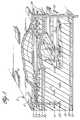
- a multi-layer PWB 2incorporates IC mounting pads 4 to receive VLSI chips.
- Conducting vias 6connect the pads to conductors in signal planes interconnecting the various chips in an MCM system.
- a first signal planegenerally designated 10 comprises conductors 12 having a minimum pitch 14 and a conductor width 16.
- the width and pitch of the conductors in the first signal planeis established, based on design requirements for spacing determined by analyzing the requirements for a first group of signals designated critical signals.
- Critical signalsinclude clock signals, control signals, signals requiring transmission over an extended distance on the PWB, asynchronous signals, and signals for which engineering changes are anticipated.
- the conductor widthis established to provide low resistance for the critical signals and the pitch is defined to provide minimal cross-talk to avoid false triggering.
- the dielectric 18has a minimum width 20 between signal planes for the critical signal plane 10. As shown in the drawings, signal planes exemplified by signal planes 22 and 23, employ common design characteristics with the first signal plane for critical signal routing.
- the three signal planes 10, 22 and 23are arranged with the first plane 10 at a 0° orientation, the adjacent plane 23 at 90° and the third plane 22 at 0° but offset by approximately one-half pitch from the first plane 10.
- interconnectionis bus oriented favoring one direction on certain parts of the board.
- Higher density interconnectis obtained by running two sets of signal traces in one direction and one set of signal traces at right angles to the first.
- the two sets of wires that run in the same directionare placed adjacent the ground planes, while the single intermediate set is rotated 90° to the first. This can be described as an "x-y-x" or "y-x-y” orientation.
- the cross-talk between wires in any planeis dictated by the relatively large spacing between the wires.
- the cross-talk between the first and second layer or second and third layeris reduced because the signals are at right angles to one another and therefore have a small area of overlap.
- FIGS. 3a and 3bPrior art technologies provided for "x-y” orientations of signal planes intermediate ground or power planes with the "x” and “y” layers oriented at 90°.
- This prior art configurationis shown in FIGS. 3a and 3b.
- the top view FIG. 3a of the "x-y” approachdemonstrates the very small overlap area of the wires in the two signal planes which is represented in section in FIG. 3b.
- FIGS. 4a and 4bwhich is known in the "x-y-r-s” approach, wherein the "x” layer 40 is oriented at 0° while the "y” layer 42 is oriented at 90°.
- the "r” layer 44is oriented at -45° while the "s” layer 46 is oriented at +45°. All four layers are placed intermediate ground planes 38 in this arrangement.
- the shaded overlap area best seen in the top view of FIG. 4arepresents the small cross-talk area also shown in the sectional view of FIG. 4b.
- the cross-talk between wires in the "y” layer 10 and the "x” layer 23is minimized based on the perpendicular orientation of those two layers.
- cross-talk between the "x" layer 23 and the "y'” layer 22is minimized based on similar perpendicular orientation.
- Cross-talk between the "y” layer 10 and the "y'” layer 22is minimized by placing the wires in an offset of approximately one-half pitch. Additional reduction in cross-talk is accomplished based on greater spacing between wires in the "y” and "y'” layers due to the combination of the distance created by the intermediate layer and offset pitch. As best seen in the top view FIG.
- the cross-talk overlap between the "y” and “x” and “x” and “y'” layers shown by first shading 48 and the cross-talk area between "y” and “y'” layers denoted by second shading 50is minimal.
- Cross-talk between the "y” and “y'” layerswill be comparable to cross-talk between wires within the same signal plane.
- the "y-x-y'" orientationallows maximum asymmetric connectivity with a minimum number of layers.
- a second signal plane generally designated 24is provided with minimum conductor spacing 26 and variable conductor widths based on design rules established for non-critical signals.
- Non-critical signalsinclude data buses and other signals less susceptible to cross-talk or false triggering and routed for only short lengths.
- a one to two chip crossingis established as a maximum for conductors in the second signal plane.
- the conductors in the second signal planeemploy narrow traces, typically 5 ⁇ m, with relatively narrow separation of the conductors of 5 to 20 ⁇ m. Density of conductors in the second signal plane is established at approximately four times the density of the first signal plane as determined by system requirements.
- a design requirement for series termination residing in the VLSI chip connected to conductors in the second signal planeeliminates requirements for termination resistors or similar means which would require a reduction in density for physical connection.
- a design rule establishing vias only between adjacent planesfurther avoids any requirement for density reduction.
- the design rules on the second signal planeallow relatively high cross-talk and have relatively high conductor resistance based on trace dimensions. The limitations on conductor length and depth of vias avoid significant impact on signal quality.
- Signal planes employing the design rules for the second signal plane exemplified by the planes generally designated 28 and 29 oriented in a "y-x-y'" relationship with the second signal plane 24 as previously described for signal planes 10, 22 and 23,are present in the PWB.
- the pitch and conductor size employedis designed to accommodate jumper wiring between conductors and disconnection of conductors using mechanical severing, laser vaporization, or other standard means.
- the embodiment of the PWB shown in the drawingsincorporates dual stripline technology having power and ground planes 30 and 32 separating "y-x-y'" groupings of signal planes.
- the present inventionis equally applicable to embodiments employing buried microstrip applications or combined applications.
- first signal plane and second signal planerequires separation of signals into designated categories as critical signals or non-critical signals. Determination of worst case requirements for critical signals establishes the design parameters for conductor dimensions, conductor pitch or spacing, and dielectric thickness between adjacent signal planes. Standard CAD systems are employed for routing of the first signal plane and signal planes having identical characteristic requirements.
- design rulesare established for the non-critical signals and standard CAD systems are employed to provide routing of the second signal plane and planes having identical signal characteristics. While two signal plane types have been demonstrated in the embodiments shown in the drawings, the present invention is applicable to a plurality of signal plane types having varying conductor densities and mechanical and electrical properties to accommodate a plurality of signal groupings having various levels of criticality and the associated design requirements imposed upon the signal planes carrying the signal group.
- the present inventionprovides for high density signal planes for signal nets of non-critical signals which comprise 70-80% of interconnections in modern MCM systems.
- the remaining critical signalsare accommodated in signal planes incorporating design rules sufficient to minimise signal degradation.
- the combined conductor density provided by the present invention for the overall PWB for the MCM systemis significantly enhanced over prior art systems employing a single design criterion for all signal planes based on critical signal requirements.
- Orientation of the "y-x-y'" groupings of signal planesmay be varied between the groups of signal planes employing various design rules based on the favored direction for bus interconnection for those conductors.
- the combination of "y-x-y'" orientation with multiple design rules for critical signal planes and high density non-critical signal planesallows maximum density in the overall PWB for the MCM system.
Landscapes
- Physics & Mathematics (AREA)
- Condensed Matter Physics & Semiconductors (AREA)
- General Physics & Mathematics (AREA)
- Engineering & Computer Science (AREA)
- Computer Hardware Design (AREA)
- Microelectronics & Electronic Packaging (AREA)
- Power Engineering (AREA)
- Geometry (AREA)
- Production Of Multi-Layered Print Wiring Board (AREA)
Abstract
Description
- The present invention relates generally to the field of printed wiring boards for Multi-Chip Module (MCM) systems for the attachment of and signal distribution between multiple integrated circuit chips. In particular, the present invention provides a method for design of a multi-layer printed wiring board.
- Mounting and interconnection of modern integrated circuits is typically accomplished through the use of Printed Wiring Boards (PWB). The connection of numerous chips in modern MCM systems for high performance computers requires multi-layer PWBs and the technological requirements for increased chip density, higher signal frequencies, and increased design complexity place high demands on PWB design techniques and manufacturing processes. The desired capabilities of PWBs are low resistance, constant transmission line impedance, high density of conductors, low cross-talk between conductors, high propagation velocity, low signal timing skew between multiple paths, ability to terminate lines in a characteristic impedance, and engineering change capability.
- Development of a PWB requires engineering trade-offs between the desired characteristics. Simultaneously achieving the desired characteristics is difficult. Low resistance and low cross-talk are incompatible with high density of conductors. Similarly, desire for high propagation velocity in combination with high density necessarily reduces the capability to perform engineering changes without redesign of PWB layers.
- Various manufacturing and design techniques for multi-layer PWBs exist. Stripline and microstrip technologies are used singly or in combination in multi-layer PWBs for control of cross-talk and impedance. Buried microstrip technology and dual stripline technology are exemplary of improvements in the art to further refine basic design capabilities for multi-layer PWBs.
- The complex routing of conductors in the various layers and between layers, and the extremely high density necessary in modern PWBs typically requires the use of Computer Aided Design (CAD) systems for generation of the PWB layouts. CAD systems employing gridded design and gridless design have been employed for modern designs. Gridded systems require placement of conductors on a given grid spacing while allowing differing conductor width. Gridless systems typically employ a fixed separation of conductors while similarly allowing varying conductor widths. Present CAD systems employ identical mechanical and electrical characteristics such as pitch of the conductors and impedance for a given PWB layout. Design compromises for allowing all types of signals such as data, clock signals, and control signals, whether synchronous or asynchronous, are made to allow the signals to be carried in the signal planes. Consequently, an over design condition exists for many signals in order to accommodate requirements of asynchronous signals or clock signals for reduced cross-talk to avoid false triggering of these critical signals.
- Arrangement on multi-layer printed circuit boards typically employs two layers between adjacent power or ground planes. These signal layers are arranged in a perpendicular relationship typically identified as "xy" to minimize cross-talk between the "x" and "y" layer based on the small overlap area between the "x" and "y" conductors. Additional layering intermediate adjacent power or ground planes has been accomplished in the prior art by addition of layers oriented at ±45° with respect to the "x" and "y" layers (typically known as "r" and "s" layers). Cross-talk is again minimized between all layers; "r", "s", "x" and "y" because of small area overlap.
- These layer orientations, while minimizing cross-talk, do not provide sufficient flexibility in modern design scenarios.
- The present invention can reduce inefficiencies of over-design required by the prior art design techniques for PWBs. For implementation of the present invention, signals are categorized based on criticality and sensitivity to cross-talk and line resistance. A first signal plane having a first conductor pitch and dielectric thickness is provided for critical signals. A second signal plane having a conductor density of approximately a factor of four greater than the first signal plane and reduced dielectric thickness is provided for non-critical signals.
- CAD design of the first signal plane and second signal plane is implemented by employing separate design rules for the two planes as opposed to common design rules for all signal planes in the PWB.
- Signals employed in the MCM are categorized based on the nature and sensitivity of the signals. Clock signals, control signals, asynchronous signals, and signals requiring transmission over a significant distance are exemplary of critical signals combined in a first category. Signals having a short transmission length and low sensitivity to cross-talk which can accommodate a conductor density of at least a factor of four over the critical signals are categorized in a second category as non-critical signals.
- Design rules for the first category of critical signals are defined to require low resistance and low noise or cross-talk to establish the mechanical and electrical characteristics of the first signal plane. Design rules for the non-critical signals allow narrow traces with narrow separation for maximum conductor density over short length runs. Additional design criteria, including limiting vias to adjacent planes only and requiring chip resident series termination further establish design rules for the non-critical signal planes to achieve maximum density. Design rules employed for the first and second signal planes are then implemented for a plurality of mixed planes having characteristics of the first signal plane and second signal plane.
- Additional density in an MCM is provided in the present invention by employing at least three signal layers, intermediate the ground or power planes, oriented in a "y-x-y'" arrangement wherein in the "y" and "y'" layers are perpendicular to the "x" layer and the "y" and "y'" layers are offset by approximately one-half pitch. The "y-x-y'" arrangement of layers intermediate the ground or power planes provides for maximum density with reduced cross-talk between layers. The present invention provides the capability to design high density MCM systems with greater miniaturization while maintaining signal integrity and adapting available design processes for cost effective implementation.
- Thus, the method of the present invention can provide a printed wiring board having distinct signal planes with differing mechanical and electrical characteristics, based on requirements of signals to be carried in the respective planes.
- Reference is made, by way of example, to the accompanying drawings in which:-
- Fig.1 is a pictorial cutaway sectional view of a multi-chip module PWB demonstrating multiple signal planes having a first pitch with low density for critical signals and multiple signal planes having a second pitch with higher density for non-critical signals, the multiple signal planes of both first and second pitch having a "y-x-y'" orientation for reduced cross-talk;
- Fig. 2 is an end section view of the PWB signal planes in Fig. 1;
- Figs. 3a and 3b are top and section views of a prior art PWB using two-layer signal plane technology employing "x-y" orientation;
- Figs. 4a and 4b are top and section views illustrating a prior art PWB employing four signal layers having "x-y-r-s" orientation wherein the "x" and "y" layers are placed at 0° and 90° while the "r" and "s" layers are oriented at +/-45°; and
- Figs. 5a and 5b are top and section views illustrating an embodiment of the present invention employing a "y-x-y'" signal layer arrangement schematically demonstrating the cross-talk areas and distances for the various layers wherein the "y" and "x" layers are oriented at 90° and the "y'" layer is offset one-half pitch from the "y" layer.
- The drawings illustrate an embodiment of the present invention in a multi-layer PWB. A
multi-layer PWB 2 incorporates IC mounting pads 4 to receive VLSI chips. Conducting vias 6 connect the pads to conductors in signal planes interconnecting the various chips in an MCM system. As best seen in FIG. 2, a first signal plane generally designated 10 comprises conductors 12 having a minimum pitch 14 and a conductor width 16. The width and pitch of the conductors in the first signal plane is established, based on design requirements for spacing determined by analyzing the requirements for a first group of signals designated critical signals. Critical signals include clock signals, control signals, signals requiring transmission over an extended distance on the PWB, asynchronous signals, and signals for which engineering changes are anticipated. The conductor width is established to provide low resistance for the critical signals and the pitch is defined to provide minimal cross-talk to avoid false triggering. The dielectric 18 has a minimum width 20 between signal planes for thecritical signal plane 10. As shown in the drawings, signal planes exemplified bysignal planes - The three
signal planes first plane 10 at a 0° orientation, theadjacent plane 23 at 90° and thethird plane 22 at 0° but offset by approximately one-half pitch from thefirst plane 10. In modern VLSI, interconnection is bus oriented favoring one direction on certain parts of the board. Higher density interconnect is obtained by running two sets of signal traces in one direction and one set of signal traces at right angles to the first. The two sets of wires that run in the same direction are placed adjacent the ground planes, while the single intermediate set is rotated 90° to the first. This can be described as an "x-y-x" or "y-x-y" orientation. The cross-talk between wires in any plane is dictated by the relatively large spacing between the wires. The cross-talk between the first and second layer or second and third layer is reduced because the signals are at right angles to one another and therefore have a small area of overlap. - Prior art technologies provided for "x-y" orientations of signal planes intermediate ground or power planes with the "x" and "y" layers oriented at 90°. This prior art configuration is shown in FIGS. 3a and 3b. The top view FIG. 3a of the "x-y" approach demonstrates the very small overlap area of the wires in the two signal planes which is represented in section in FIG. 3b. A more sophisticated prior art technique is shown in FIGS. 4a and 4b, which is known in the "x-y-r-s" approach, wherein the "x"
layer 40 is oriented at 0° while the "y"layer 42 is oriented at 90°. The "r"layer 44 is oriented at -45° while the "s"layer 46 is oriented at +45°. All four layers are placed intermediate ground planes 38 in this arrangement. Again, the shaded overlap area best seen in the top view of FIG. 4a represents the small cross-talk area also shown in the sectional view of FIG. 4b. - In the present invention, the cross-talk between wires in the "y"
layer 10 and the "x"layer 23 is minimized based on the perpendicular orientation of those two layers. Similarly, cross-talk between the "x"layer 23 and the "y'"layer 22 is minimized based on similar perpendicular orientation. Cross-talk between the "y"layer 10 and the "y'"layer 22 is minimized by placing the wires in an offset of approximately one-half pitch. Additional reduction in cross-talk is accomplished based on greater spacing between wires in the "y" and "y'" layers due to the combination of the distance created by the intermediate layer and offset pitch. As best seen in the top view FIG. 5a, the cross-talk overlap between the "y" and "x" and "x" and "y'" layers shown byfirst shading 48 and the cross-talk area between "y" and "y'" layers denoted bysecond shading 50 is minimal. Cross-talk between the "y" and "y'" layers will be comparable to cross-talk between wires within the same signal plane. The "y-x-y'" orientation allows maximum asymmetric connectivity with a minimum number of layers. - A second signal plane generally designated 24 is provided with minimum conductor spacing 26 and variable conductor widths based on design rules established for non-critical signals. Non-critical signals include data buses and other signals less susceptible to cross-talk or false triggering and routed for only short lengths. Typically, a one to two chip crossing is established as a maximum for conductors in the second signal plane. The conductors in the second signal plane employ narrow traces, typically 5 µm, with relatively narrow separation of the conductors of 5 to 20 µm. Density of conductors in the second signal plane is established at approximately four times the density of the first signal plane as determined by system requirements. A design requirement for series termination residing in the VLSI chip connected to conductors in the second signal plane eliminates requirements for termination resistors or similar means which would require a reduction in density for physical connection. A design rule establishing vias only between adjacent planes further avoids any requirement for density reduction. The design rules on the second signal plane allow relatively high cross-talk and have relatively high conductor resistance based on trace dimensions. The limitations on conductor length and depth of vias avoid significant impact on signal quality. Signal planes employing the design rules for the second signal plane exemplified by the planes generally designated 28 and 29 oriented in a "y-x-y'" relationship with the
second signal plane 24 as previously described forsignal planes - Engineering changes are accommodated in the first signal plane and signal planes employing the design rules for the first signal plane. The pitch and conductor size employed is designed to accommodate jumper wiring between conductors and disconnection of conductors using mechanical severing, laser vaporization, or other standard means.
- The embodiment of the PWB shown in the drawings incorporates dual stripline technology having power and
ground planes - Establishing design rules for the first signal plane and second signal plane requires separation of signals into designated categories as critical signals or non-critical signals. Determination of worst case requirements for critical signals establishes the design parameters for conductor dimensions, conductor pitch or spacing, and dielectric thickness between adjacent signal planes. Standard CAD systems are employed for routing of the first signal plane and signal planes having identical characteristic requirements.
- Similarly, design rules are established for the non-critical signals and standard CAD systems are employed to provide routing of the second signal plane and planes having identical signal characteristics. While two signal plane types have been demonstrated in the embodiments shown in the drawings, the present invention is applicable to a plurality of signal plane types having varying conductor densities and mechanical and electrical properties to accommodate a plurality of signal groupings having various levels of criticality and the associated design requirements imposed upon the signal planes carrying the signal group.
- The present invention provides for high density signal planes for signal nets of non-critical signals which comprise 70-80% of interconnections in modern MCM systems. The remaining critical signals are accommodated in signal planes incorporating design rules sufficient to minimise signal degradation. The combined conductor density provided by the present invention for the overall PWB for the MCM system is significantly enhanced over prior art systems employing a single design criterion for all signal planes based on critical signal requirements.
- Orientation of the "y-x-y'" groupings of signal planes may be varied between the groups of signal planes employing various design rules based on the favored direction for bus interconnection for those conductors. The combination of "y-x-y'" orientation with multiple design rules for critical signal planes and high density non-critical signal planes allows maximum density in the overall PWB for the MCM system.
- Those skilled in the art will recognize modifications and substitutions to the embodiments disclosed herein for specific applications. Such modifications and substitutions are within the scope of the present invention as defined in the following claims.
Claims (16)
- A method for multi-layer printed wiring board design comprising the steps of:
establishing a first category of critical signals;
defining design rules for first conductor spacing and first conductor characteristics to meet requirements for avoiding degradation of the critical signals;
laying out at least one first signal plane using the first design rules;
defining second design rules for second conductor spacing and second conductor characteristics for signals not categorized as critical signals; and
laying out at least one second signal plane employing the second design rules. - A method as defined in claim 1, wherein the step of establishing the first category of critical signals includes selecting, as critical signals, clock signals, control signals, and asynchronous signals.
- A method as defined in claim 1 or 2, wherein the step of establishing the first category of critical signals further includes selecting signals requiring vias of greater than one layer.
- A method as defined in claim 1, 2, or 3, wherein the step of establishing the first category of critical signals further includes selecting signals having a path extending beyond two chips in length.
- A method as defined in claim 1, 2, 3, or 4, wherein the step of defining second design rules comprises determining second conductor spacing and second conductor characteristics to establish a conductor density of at by the first conductor spacing and first conductor characteristics.
- A method as defined in any preceding claim, wherein the step of establishing the first category of critical signals includes selecting signals potentially requiring engineering changes.
- A method as defined in any preceding claim, wherein the step of establishing the first category of critical signals includes selecting signals requiring off-chip termination.
- A method for multi-layer printed wiring board design comprising the steps of:
establishing a first category of critical signals;
defining design rules for first conductor spacing and first conductor characteristics to meet requirements for avoiding degradation of the critical signals;
identifying a favored direction for bus interconnection;
defining a first orientation of adjacent signal planes to employ the first design rules having at least one "y" plane oriented at substantially 0° relative to the favored direction, at least one "x" plane having conductors oriented at substantially 90° to the favored direction and at least one "y'" plane having conductors oriented at substantially 0° with respect to the favored direction, said conductors of the "y'" plane offset from the conductors of the "y" plane by approximately one-half pitch;
laying out at least one plurality of first signal planes using the first design rules and first orientation,
defining second design rules for second conductor spacing and second conductor characteristics for signals not categorized as critical signals; and
laying out at least one plurality of second signal planes employing the second design rules. - A method as defined in claim 8, further comprising the steps of:
identifying a second favored direction for bus interconnection;
defining a second orientation of adjacent signal planes to employ the second design rules having at least one second "y" plane oriented at substantially 0° relative to the favored direction, at least one second "x" plane having conductors oriented at substantially 90° to the favored direction and at least one second "y'" plane having conductors oriented at substantially 0° with respect to the favored direction, said conductors of the second "y'" plane offset from the conductors of the second "y" plane by approximately one-half pitch; and wherein said step of laying out at least one plurality of second signal planes employs said second orientation. - A method as defined in claim 8 or 9, wherein the step of establishing the first category of critical signals includes selecting, as critical signals, clock signals, control signals, and asynchronous signals.
- A method as defined in claim 8, 9, or 10, wherein the step of establishing the first category of critical signals further includes selecting signals requiring vias of greater than one layer.
- A method as defined in claim 8, 9, 10, or 11, wherein the step of selecting the first category of critical signals further includes selecting signals having a path extending beyond two chips in length.
- A method as defined in any of claims 8 to 12, wherein the step of defining second design rules comprises determining second conductor spacing and second conductor characteristics to establish a conductor density of at least a factor of four greater than the density established by the first conductor spacing and first conductor characteristics.
- A method as defined in any of claims 8 to 13, wherein the step of establishing the first category of critical signals includes selecting signals potentially requiring engineering changes.
- A method as defined in any of claims 8 to 14, wherein the step of establishing the first category of critical signals includes selecting signals requiring off-chip termination.
- A multi-layer printed wiring board, designed by the method of any one of the preceding claims.
Applications Claiming Priority (2)
| Application Number | Priority Date | Filing Date | Title |
|---|---|---|---|
| US08/125,035US5508938A (en) | 1992-08-13 | 1993-09-21 | Special interconnect layer employing offset trace layout for advanced multi-chip module packages |
| US125035 | 1993-09-21 |
Publications (2)
| Publication Number | Publication Date |
|---|---|
| EP0644596A1true EP0644596A1 (en) | 1995-03-22 |
| EP0644596B1 EP0644596B1 (en) | 1999-11-17 |
Family
ID=22417927
Family Applications (1)
| Application Number | Title | Priority Date | Filing Date |
|---|---|---|---|
| EP94113128AExpired - LifetimeEP0644596B1 (en) | 1993-09-21 | 1994-08-23 | Method for multi-layer printed wiring board design |
Country Status (4)
| Country | Link |
|---|---|
| US (1) | US5508938A (en) |
| EP (1) | EP0644596B1 (en) |
| JP (1) | JP3238831B2 (en) |
| DE (1) | DE69421658T2 (en) |
Cited By (1)
| Publication number | Priority date | Publication date | Assignee | Title |
|---|---|---|---|---|
| DE10031658A1 (en)* | 2000-06-29 | 2002-01-17 | Siemens Ag | Microwave module comprising substrate with HF and LF layers forming distribution network structures, includes intervening insulating layer |
Families Citing this family (80)
| Publication number | Priority date | Publication date | Assignee | Title |
|---|---|---|---|---|
| JP2638567B2 (en)* | 1995-06-08 | 1997-08-06 | 日本電気株式会社 | Multilayer wiring board |
| US5786630A (en)* | 1996-08-07 | 1998-07-28 | Intel Corporation | Multi-layer C4 flip-chip substrate |
| US6307162B1 (en) | 1996-12-09 | 2001-10-23 | International Business Machines Corporation | Integrated circuit wiring |
| US5987241A (en)* | 1997-01-09 | 1999-11-16 | Hewlett-Packard Company | Routing techniques to assure electrical integrity in datapath blocks |
| US7321485B2 (en) | 1997-04-08 | 2008-01-22 | X2Y Attenuators, Llc | Arrangement for energy conditioning |
| US7336468B2 (en) | 1997-04-08 | 2008-02-26 | X2Y Attenuators, Llc | Arrangement for energy conditioning |
| US9054094B2 (en) | 1997-04-08 | 2015-06-09 | X2Y Attenuators, Llc | Energy conditioning circuit arrangement for integrated circuit |
| US5874778A (en)* | 1997-06-11 | 1999-02-23 | International Business Machines Corporation | Embedded power and ground plane structure |
| US6691296B1 (en)* | 1998-02-02 | 2004-02-10 | Matsushita Electric Industrial Co., Ltd. | Circuit board design aiding |
| DE19835263C2 (en)* | 1998-08-04 | 2000-06-21 | Siemens Ag | Integrated circuit with electrical connections that can be separated by the action of energy |
| JP4363716B2 (en)* | 1999-06-25 | 2009-11-11 | 株式会社東芝 | LSI wiring structure design method |
| US6392159B1 (en) | 1999-07-27 | 2002-05-21 | International Business Machines Corporation | Embedded structure for engineering change and repair of circuit boards |
| US7334326B1 (en) | 2001-06-19 | 2008-02-26 | Amkor Technology, Inc. | Method for making an integrated circuit substrate having embedded passive components |
| US6930256B1 (en) | 2002-05-01 | 2005-08-16 | Amkor Technology, Inc. | Integrated circuit substrate having laser-embedded conductive patterns and method therefor |
| US6987661B1 (en) | 2001-06-19 | 2006-01-17 | Amkor Technology, Inc. | Integrated circuit substrate having embedded passive components and methods therefor |
| US6831371B1 (en) | 2002-03-16 | 2004-12-14 | Amkor Technology, Inc. | Integrated circuit substrate having embedded wire conductors and method therefor |
| US20080043447A1 (en)* | 2002-05-01 | 2008-02-21 | Amkor Technology, Inc. | Semiconductor package having laser-embedded terminals |
| US7548430B1 (en) | 2002-05-01 | 2009-06-16 | Amkor Technology, Inc. | Buildup dielectric and metallization process and semiconductor package |
| US9691635B1 (en) | 2002-05-01 | 2017-06-27 | Amkor Technology, Inc. | Buildup dielectric layer having metallization pattern semiconductor package fabrication method |
| US6930257B1 (en) | 2002-05-01 | 2005-08-16 | Amkor Technology, Inc. | Integrated circuit substrate having laminated laser-embedded circuit layers |
| US7633765B1 (en) | 2004-03-23 | 2009-12-15 | Amkor Technology, Inc. | Semiconductor package including a top-surface metal layer for implementing circuit features |
| US7028400B1 (en) | 2002-05-01 | 2006-04-18 | Amkor Technology, Inc. | Integrated circuit substrate having laser-exposed terminals |
| US7399661B2 (en)* | 2002-05-01 | 2008-07-15 | Amkor Technology, Inc. | Method for making an integrated circuit substrate having embedded back-side access conductors and vias |
| US7670962B2 (en) | 2002-05-01 | 2010-03-02 | Amkor Technology, Inc. | Substrate having stiffener fabrication method |
| US7243328B2 (en)* | 2003-05-07 | 2007-07-10 | Cadence Design Systems, Inc. | Method and apparatus for representing items in a design layout |
| US7080339B2 (en)* | 2003-05-07 | 2006-07-18 | Cadence Design Systems, Inc. | Plane representation of wiring in a design layout |
| US7065731B2 (en)* | 2003-05-07 | 2006-06-20 | Cadence Design Systems, Inc. | Removal of acute angles in a design layout |
| US11081370B2 (en) | 2004-03-23 | 2021-08-03 | Amkor Technology Singapore Holding Pte. Ltd. | Methods of manufacturing an encapsulated semiconductor device |
| US10811277B2 (en) | 2004-03-23 | 2020-10-20 | Amkor Technology, Inc. | Encapsulated semiconductor package |
| US7145238B1 (en) | 2004-05-05 | 2006-12-05 | Amkor Technology, Inc. | Semiconductor package and substrate having multi-level vias |
| TWI237380B (en)* | 2004-11-19 | 2005-08-01 | Advanced Semiconductor Eng | Build-up via for suppressing simultaneous switching noise |
| JP2008535207A (en) | 2005-03-01 | 2008-08-28 | エックストゥーワイ アテニュエイターズ,エルエルシー | Regulator with coplanar conductor |
| US7571408B1 (en) | 2005-03-09 | 2009-08-04 | Cadence Design Systems, Inc. | Methods and apparatus for diagonal route shielding |
| US7348667B2 (en)* | 2005-03-22 | 2008-03-25 | International Business Machines Corporation | System and method for noise reduction in multi-layer ceramic packages |
| US7307437B1 (en)* | 2005-03-24 | 2007-12-11 | Hewlett-Packard Development Company, L.P. | Arrangement with conductive pad embedment |
| US8826531B1 (en) | 2005-04-05 | 2014-09-09 | Amkor Technology, Inc. | Method for making an integrated circuit substrate having laminated laser-embedded circuit layers |
| US7430800B2 (en)* | 2005-06-06 | 2008-10-07 | International Business Machines Corporation | Apparatus and method for far end noise reduction using capacitive cancellation by offset wiring |
| US7694258B1 (en) | 2005-08-01 | 2010-04-06 | Cadence Design Systems, Inc. | Method and apparatus for inserting metal fill in an integrated circuit (“IC”) layout |
| US7589398B1 (en) | 2006-10-04 | 2009-09-15 | Amkor Technology, Inc. | Embedded metal features structure |
| US7550857B1 (en) | 2006-11-16 | 2009-06-23 | Amkor Technology, Inc. | Stacked redistribution layer (RDL) die assembly package |
| US7750250B1 (en) | 2006-12-22 | 2010-07-06 | Amkor Technology, Inc. | Blind via capture pad structure |
| US7608538B2 (en)* | 2007-01-05 | 2009-10-27 | International Business Machines Corporation | Formation of vertical devices by electroplating |
| US7752752B1 (en) | 2007-01-09 | 2010-07-13 | Amkor Technology, Inc. | Method of fabricating an embedded circuit pattern |
| US8018052B2 (en)* | 2007-06-29 | 2011-09-13 | Stats Chippac Ltd. | Integrated circuit package system with side substrate having a top layer |
| US8323771B1 (en) | 2007-08-15 | 2012-12-04 | Amkor Technology, Inc. | Straight conductor blind via capture pad structure and fabrication method |
| CN101257788B (en)* | 2007-12-07 | 2010-07-14 | 深圳创维-Rgb电子有限公司 | A method, system and equipment for automatic plug-in on PCB |
| US8872329B1 (en) | 2009-01-09 | 2014-10-28 | Amkor Technology, Inc. | Extended landing pad substrate package structure and method |
| US7960827B1 (en) | 2009-04-09 | 2011-06-14 | Amkor Technology, Inc. | Thermal via heat spreader package and method |
| US8623753B1 (en) | 2009-05-28 | 2014-01-07 | Amkor Technology, Inc. | Stackable protruding via package and method |
| US8222538B1 (en) | 2009-06-12 | 2012-07-17 | Amkor Technology, Inc. | Stackable via package and method |
| US8471154B1 (en) | 2009-08-06 | 2013-06-25 | Amkor Technology, Inc. | Stackable variable height via package and method |
| US8796561B1 (en) | 2009-10-05 | 2014-08-05 | Amkor Technology, Inc. | Fan out build up substrate stackable package and method |
| US8288657B2 (en)* | 2009-10-12 | 2012-10-16 | International Business Machines Corporation | Noise coupling reduction and impedance discontinuity control in high-speed ceramic modules |
| US8937381B1 (en) | 2009-12-03 | 2015-01-20 | Amkor Technology, Inc. | Thin stackable package and method |
| US9691734B1 (en) | 2009-12-07 | 2017-06-27 | Amkor Technology, Inc. | Method of forming a plurality of electronic component packages |
| US8536462B1 (en) | 2010-01-22 | 2013-09-17 | Amkor Technology, Inc. | Flex circuit package and method |
| JP5486376B2 (en)* | 2010-03-31 | 2014-05-07 | ルネサスエレクトロニクス株式会社 | Semiconductor device |
| US8300423B1 (en) | 2010-05-25 | 2012-10-30 | Amkor Technology, Inc. | Stackable treated via package and method |
| US8294276B1 (en) | 2010-05-27 | 2012-10-23 | Amkor Technology, Inc. | Semiconductor device and fabricating method thereof |
| US8338229B1 (en) | 2010-07-30 | 2012-12-25 | Amkor Technology, Inc. | Stackable plasma cleaned via package and method |
| US8717775B1 (en) | 2010-08-02 | 2014-05-06 | Amkor Technology, Inc. | Fingerprint sensor package and method |
| US8337657B1 (en) | 2010-10-27 | 2012-12-25 | Amkor Technology, Inc. | Mechanical tape separation package and method |
| US8482134B1 (en) | 2010-11-01 | 2013-07-09 | Amkor Technology, Inc. | Stackable package and method |
| US9748154B1 (en) | 2010-11-04 | 2017-08-29 | Amkor Technology, Inc. | Wafer level fan out semiconductor device and manufacturing method thereof |
| US8525318B1 (en) | 2010-11-10 | 2013-09-03 | Amkor Technology, Inc. | Semiconductor device and fabricating method thereof |
| US8557629B1 (en) | 2010-12-03 | 2013-10-15 | Amkor Technology, Inc. | Semiconductor device having overlapped via apertures |
| US8535961B1 (en) | 2010-12-09 | 2013-09-17 | Amkor Technology, Inc. | Light emitting diode (LED) package and method |
| US9721872B1 (en) | 2011-02-18 | 2017-08-01 | Amkor Technology, Inc. | Methods and structures for increasing the allowable die size in TMV packages |
| US9013011B1 (en) | 2011-03-11 | 2015-04-21 | Amkor Technology, Inc. | Stacked and staggered die MEMS package and method |
| KR101140113B1 (en) | 2011-04-26 | 2012-04-30 | 앰코 테크놀로지 코리아 주식회사 | Semiconductor device |
| US8653674B1 (en) | 2011-09-15 | 2014-02-18 | Amkor Technology, Inc. | Electronic component package fabrication method and structure |
| US8633598B1 (en) | 2011-09-20 | 2014-01-21 | Amkor Technology, Inc. | Underfill contacting stacking balls package fabrication method and structure |
| US9029962B1 (en) | 2011-10-12 | 2015-05-12 | Amkor Technology, Inc. | Molded cavity substrate MEMS package fabrication method and structure |
| KR101366461B1 (en) | 2012-11-20 | 2014-02-26 | 앰코 테크놀로지 코리아 주식회사 | Semiconductor device and manufacturing method thereof |
| US9799592B2 (en) | 2013-11-19 | 2017-10-24 | Amkor Technology, Inc. | Semicondutor device with through-silicon via-less deep wells |
| KR101488590B1 (en) | 2013-03-29 | 2015-01-30 | 앰코 테크놀로지 코리아 주식회사 | Semiconductor device and manufacturing method thereof |
| US9331016B2 (en) | 2013-07-25 | 2016-05-03 | Qualcomm Incorporated | SOC design with critical technology pitch alignment |
| KR101607981B1 (en) | 2013-11-04 | 2016-03-31 | 앰코 테크놀로지 코리아 주식회사 | Interposer and method for manufacturing the same, and semiconductor package using the same |
| US9960328B2 (en) | 2016-09-06 | 2018-05-01 | Amkor Technology, Inc. | Semiconductor device and manufacturing method thereof |
| DE102019212785A1 (en)* | 2019-08-27 | 2021-03-04 | Robert Bosch Gmbh | Method and device for analyzing a product |
Citations (7)
| Publication number | Priority date | Publication date | Assignee | Title |
|---|---|---|---|---|
| EP0026807A1 (en)* | 1979-10-06 | 1981-04-15 | International Business Machines Corporation | Multilayer module with constant characteristic wave impedance |
| JPS58124260A (en)* | 1982-01-20 | 1983-07-23 | Nec Corp | Circuit board |
| FR2563656A1 (en)* | 1984-04-27 | 1985-10-31 | Nec Corp | LARGE-SCALE INTEGRATION CIRCUIT BLOCK |
| EP0166289A2 (en)* | 1984-06-29 | 1986-01-02 | International Business Machines Corporation | High density module for semiconductor device chips |
| FR2567684A1 (en)* | 1984-07-10 | 1986-01-17 | Nec Corp | MODULE HAVING A MULTILAYER CERAMIC SUBSTRATE AND A MULTILAYER CIRCUIT ON THE SUBSTRATE AND METHOD FOR THE PRODUCTION THEREOF |
| DE4021965A1 (en)* | 1989-07-10 | 1991-01-24 | Hitachi Ltd | THICK LAYER / THICK LAYER COMPOSITE SUBSTRATE AND ELECTRONIC CIRCUIT USING THIS SUBSTRATE |
| EP0558984A2 (en)* | 1992-03-06 | 1993-09-08 | International Business Machines Corporation | Hybrid ceramic thin-film module structure |
Family Cites Families (23)
| Publication number | Priority date | Publication date | Assignee | Title |
|---|---|---|---|---|
| US4210885A (en)* | 1978-06-30 | 1980-07-01 | International Business Machines Corporation | Thin film lossy line for preventing reflections in microcircuit chip package interconnections |
| US4245273A (en)* | 1979-06-29 | 1981-01-13 | International Business Machines Corporation | Package for mounting and interconnecting a plurality of large scale integrated semiconductor devices |
| US4553111A (en)* | 1983-08-30 | 1985-11-12 | Burroughs Corporation | Printed circuit board maximizing areas for component utilization |
| US4560962A (en)* | 1983-08-30 | 1985-12-24 | Burroughs Corporation | Multilayered printed circuit board with controlled 100 ohm impedance |
| EP0257119B1 (en)* | 1986-08-22 | 1991-02-20 | Ibm Deutschland Gmbh | Integrated wiring system for vlsi |
| US4811082A (en)* | 1986-11-12 | 1989-03-07 | International Business Machines Corporation | High performance integrated circuit packaging structure |
| JPS63245952A (en)* | 1987-04-01 | 1988-10-13 | Hitachi Ltd | Multi-chip module structure |
| JP2606845B2 (en)* | 1987-06-19 | 1997-05-07 | 富士通株式会社 | Semiconductor integrated circuit |
| US5165166A (en)* | 1987-09-29 | 1992-11-24 | Microelectronics And Computer Technology Corporation | Method of making a customizable circuitry |
| US4859806A (en)* | 1988-05-17 | 1989-08-22 | Microelectronics And Computer Technology Corporation | Discretionary interconnect |
| JPH0229124A (en)* | 1988-07-19 | 1990-01-31 | Toshiba Corp | standard cell |
| JP2668981B2 (en)* | 1988-09-19 | 1997-10-27 | 富士通株式会社 | Semiconductor integrated circuit |
| JPH02106968A (en)* | 1988-10-17 | 1990-04-19 | Hitachi Ltd | Semiconductor integrated circuit device and method for forming the same |
| JPH0731695B2 (en)* | 1988-10-26 | 1995-04-10 | 三菱電機株式会社 | Method for compacting mask pattern of semiconductor integrated circuit device |
| EP0393635B1 (en)* | 1989-04-21 | 1997-09-03 | Nec Corporation | Semiconductor device having multi-level wirings |
| US5061824A (en)* | 1989-08-23 | 1991-10-29 | Ncr Corporation | Backpanel having multiple logic family signal layers |
| US5377124A (en)* | 1989-09-20 | 1994-12-27 | Aptix Corporation | Field programmable printed circuit board |
| US5127986A (en)* | 1989-12-01 | 1992-07-07 | Cray Research, Inc. | High power, high density interconnect method and apparatus for integrated circuits |
| US5060116A (en)* | 1990-04-20 | 1991-10-22 | Grobman Warren D | Electronics system with direct write engineering change capability |
| US5081563A (en)* | 1990-04-27 | 1992-01-14 | International Business Machines Corporation | Multi-layer package incorporating a recessed cavity for a semiconductor chip |
| US5045819A (en)* | 1990-06-06 | 1991-09-03 | Arizona Board Of Regents, A Body Corporate Acting On Behalf Of Arizona State University | Multilayer-multiconductor microstrips for digital integrated circuits |
| US5068631A (en)* | 1990-08-09 | 1991-11-26 | At&T Bell Laboratories | Sub power plane to provide EMC filtering for VLSI devices |
| JP2825031B2 (en)* | 1991-08-06 | 1998-11-18 | 日本電気株式会社 | Semiconductor memory device |
- 1993
- 1993-09-21USUS08/125,035patent/US5508938A/ennot_activeExpired - Lifetime
- 1994
- 1994-08-23DEDE69421658Tpatent/DE69421658T2/ennot_activeExpired - Lifetime
- 1994-08-23EPEP94113128Apatent/EP0644596B1/ennot_activeExpired - Lifetime
- 1994-09-19JPJP22312694Apatent/JP3238831B2/ennot_activeExpired - Lifetime
Patent Citations (7)
| Publication number | Priority date | Publication date | Assignee | Title |
|---|---|---|---|---|
| EP0026807A1 (en)* | 1979-10-06 | 1981-04-15 | International Business Machines Corporation | Multilayer module with constant characteristic wave impedance |
| JPS58124260A (en)* | 1982-01-20 | 1983-07-23 | Nec Corp | Circuit board |
| FR2563656A1 (en)* | 1984-04-27 | 1985-10-31 | Nec Corp | LARGE-SCALE INTEGRATION CIRCUIT BLOCK |
| EP0166289A2 (en)* | 1984-06-29 | 1986-01-02 | International Business Machines Corporation | High density module for semiconductor device chips |
| FR2567684A1 (en)* | 1984-07-10 | 1986-01-17 | Nec Corp | MODULE HAVING A MULTILAYER CERAMIC SUBSTRATE AND A MULTILAYER CIRCUIT ON THE SUBSTRATE AND METHOD FOR THE PRODUCTION THEREOF |
| DE4021965A1 (en)* | 1989-07-10 | 1991-01-24 | Hitachi Ltd | THICK LAYER / THICK LAYER COMPOSITE SUBSTRATE AND ELECTRONIC CIRCUIT USING THIS SUBSTRATE |
| EP0558984A2 (en)* | 1992-03-06 | 1993-09-08 | International Business Machines Corporation | Hybrid ceramic thin-film module structure |
Non-Patent Citations (1)
| Title |
|---|
| PATENT ABSTRACTS OF JAPAN vol. 7, no. 236 (E - 205)<1381> 20 October 1983 (1983-10-20)* |
Cited By (1)
| Publication number | Priority date | Publication date | Assignee | Title |
|---|---|---|---|---|
| DE10031658A1 (en)* | 2000-06-29 | 2002-01-17 | Siemens Ag | Microwave module comprising substrate with HF and LF layers forming distribution network structures, includes intervening insulating layer |
Also Published As
| Publication number | Publication date |
|---|---|
| JP3238831B2 (en) | 2001-12-17 |
| DE69421658T2 (en) | 2000-03-09 |
| EP0644596B1 (en) | 1999-11-17 |
| DE69421658D1 (en) | 1999-12-23 |
| JPH07152823A (en) | 1995-06-16 |
| US5508938A (en) | 1996-04-16 |
Similar Documents
| Publication | Publication Date | Title |
|---|---|---|
| EP0644596B1 (en) | Method for multi-layer printed wiring board design | |
| US4904968A (en) | Circuit board configuration for reducing signal distortion | |
| US4782193A (en) | Polygonal wiring for improved package performance | |
| KR100301363B1 (en) | Circuit board including screen grid and constructing method of the same | |
| JP3090453B2 (en) | Thick film thin film laminated substrate and electronic circuit device using the same | |
| US7326856B2 (en) | Multi-layer wiring board | |
| US4689441A (en) | Routing method and pattern for reducing cross talk noise problems on printed interconnection boards | |
| US5077451A (en) | Custom tooled printed circuit board | |
| US5397861A (en) | Electrical interconnection board | |
| US5055973A (en) | Custom tooled printed circuit board | |
| US6538213B1 (en) | High density design for organic chip carriers | |
| WO2008014068A2 (en) | Partially plated through-holes and achieving high connectivity in multilayer circuit boards using the same | |
| US5790383A (en) | Printed circuit board | |
| US4004196A (en) | Multi-layer panel board with single-in-line package for high speed switching logic | |
| US20070180420A1 (en) | Designing a circuit apparatus with multiple propagation speeds of signals | |
| US20060067067A1 (en) | Backplane with routing to reduce layer count | |
| US20030198031A1 (en) | Optimized conductor routing for multiple components on a printed circuit board | |
| US6662250B1 (en) | Optimized routing strategy for multiple synchronous bus groups | |
| EP0637032A2 (en) | Parallel processor structure and package | |
| US20040189418A1 (en) | Method and structure for implementing enhanced differential signal trace routing | |
| Bonner et al. | Advanced printed-circuit board design for high-performance computer applications | |
| Venkatachalam | Pulse propagation properties of multilayer ceramic multichip modules for VLSI circuits | |
| US20100175911A1 (en) | High-Speed Two-Layer and Multilayer Circuit Boards | |
| US8125087B2 (en) | High-density flip-chip interconnect | |
| WO1999041770A2 (en) | Routing topology for identical connector point layouts on primary and secondary sides of a substrate |
Legal Events
| Date | Code | Title | Description |
|---|---|---|---|
| PUAI | Public reference made under article 153(3) epc to a published international application that has entered the european phase | Free format text:ORIGINAL CODE: 0009012 | |
| AK | Designated contracting states | Kind code of ref document:A1 Designated state(s):DE GB | |
| 17P | Request for examination filed | Effective date:19950607 | |
| 17Q | First examination report despatched | Effective date:19960627 | |
| GRAG | Despatch of communication of intention to grant | Free format text:ORIGINAL CODE: EPIDOS AGRA | |
| GRAG | Despatch of communication of intention to grant | Free format text:ORIGINAL CODE: EPIDOS AGRA | |
| GRAH | Despatch of communication of intention to grant a patent | Free format text:ORIGINAL CODE: EPIDOS IGRA | |
| GRAH | Despatch of communication of intention to grant a patent | Free format text:ORIGINAL CODE: EPIDOS IGRA | |
| GRAA | (expected) grant | Free format text:ORIGINAL CODE: 0009210 | |
| AK | Designated contracting states | Kind code of ref document:B1 Designated state(s):DE GB | |
| REF | Corresponds to: | Ref document number:69421658 Country of ref document:DE Date of ref document:19991223 | |
| PLBE | No opposition filed within time limit | Free format text:ORIGINAL CODE: 0009261 | |
| STAA | Information on the status of an ep patent application or granted ep patent | Free format text:STATUS: NO OPPOSITION FILED WITHIN TIME LIMIT | |
| 26N | No opposition filed | ||
| REG | Reference to a national code | Ref country code:GB Ref legal event code:IF02 | |
| PGFP | Annual fee paid to national office [announced via postgrant information from national office to epo] | Ref country code:DE Payment date:20130821 Year of fee payment:20 | |
| PGFP | Annual fee paid to national office [announced via postgrant information from national office to epo] | Ref country code:GB Payment date:20130821 Year of fee payment:20 | |
| REG | Reference to a national code | Ref country code:DE Ref legal event code:R071 Ref document number:69421658 Country of ref document:DE | |
| REG | Reference to a national code | Ref country code:GB Ref legal event code:PE20 Expiry date:20140822 | |
| PG25 | Lapsed in a contracting state [announced via postgrant information from national office to epo] | Ref country code:DE Free format text:LAPSE BECAUSE OF EXPIRATION OF PROTECTION Effective date:20140826 | |
| PG25 | Lapsed in a contracting state [announced via postgrant information from national office to epo] | Ref country code:GB Free format text:LAPSE BECAUSE OF EXPIRATION OF PROTECTION Effective date:20140822 |