EP0642238B1 - Method and apparatus for correcting phase of frames in subsriber loop carrier system - Google Patents
Method and apparatus for correcting phase of frames in subsriber loop carrier systemDownload PDFInfo
- Publication number
- EP0642238B1 EP0642238B1EP94101411AEP94101411AEP0642238B1EP 0642238 B1EP0642238 B1EP 0642238B1EP 94101411 AEP94101411 AEP 94101411AEP 94101411 AEP94101411 AEP 94101411AEP 0642238 B1EP0642238 B1EP 0642238B1
- Authority
- EP
- European Patent Office
- Prior art keywords
- phase
- multiframe
- frames
- frame
- counter
- Prior art date
- Legal status (The legal status is an assumption and is not a legal conclusion. Google has not performed a legal analysis and makes no representation as to the accuracy of the status listed.)
- Expired - Lifetime
Links
Images


Classifications
- H—ELECTRICITY
- H04—ELECTRIC COMMUNICATION TECHNIQUE
- H04Q—SELECTING
- H04Q11/00—Selecting arrangements for multiplex systems
- H04Q11/04—Selecting arrangements for multiplex systems for time-division multiplexing
- H—ELECTRICITY
- H04—ELECTRIC COMMUNICATION TECHNIQUE
- H04J—MULTIPLEX COMMUNICATION
- H04J3/00—Time-division multiplex systems
- H04J3/02—Details
- H04J3/06—Synchronising arrangements
- H04J3/0635—Clock or time synchronisation in a network
- H04J3/0676—Mutual
- H—ELECTRICITY
- H04—ELECTRIC COMMUNICATION TECHNIQUE
- H04J—MULTIPLEX COMMUNICATION
- H04J3/00—Time-division multiplex systems
- H04J3/02—Details
- H04J3/06—Synchronising arrangements
- H04J3/0635—Clock or time synchronisation in a network
- H04J3/0638—Clock or time synchronisation among nodes; Internode synchronisation
- H04J3/0647—Synchronisation among TDM nodes
Definitions
- the present inventionrelates to a method and apparatus for correcting the phase of transmitted data frames, and more particularly to a method and apparatus for correcting the phase of frames/multiframes transmitted over incoming lines in subscriber loop carrier systems.
- Subscriber loop carrier systemshave been employed to accommodate subscribers, at geographically remote locations from switching offices, economically and with high transmission quality, and also to alleviate the problem of the ever increasing number of telephone cables in urban areas.
- a plurality of subscriber linesare multiplexed as PCM data with a frame/multiframe structure at a remote terminal (RT), and the thus multiplexed PCM data are then transmitted over a fiber optic or other transmission medium to a central office terminal (COT), where the data are demultiplexed into a plurality of subscriber lines for connection to switching equipment.
- RTremote terminal
- COTcentral office terminal
- a multiplexer for remultiplexing a plurality of multiplexed datais provided with a time slot interchanger (TSI) for interchanging time slots to accomplish dynamic rearrangement on a user-by-user basis.
- TSItime slot interchanger
- phase correctionis done by storing the data in memory at the receiving end. This requires the provision of a memory for storing the data, and furthermore, transmission delays are caused because of temporarily storing the data.
- the phase correctionis only necessary for the frame, but no phase correction is needed for the multiframe. In this case, a memory that can store one frame of data will suffice for the purpose, and the transmission delay can be kept within one frame period.
- the phase correctionmust be done not only for the frame but for the multiframe that typically consists of 12 frames. In such a case, the memory capacity required will be much larger, and significant transmission delays will result.
- TCMtime compression multiplexing
- the oscillator frequency at a receiving endis controlled on the basis of advance (A), retard (R) and out-of-limits (OL) signals from the transmitting end and A, R and OL signals made at the receiving end.
- GB-A-1 577 331in which the clock frequency of a switching center receiving end is controlled based on incoming A-R-Z at a ("advance”, “retard” and “do-nothing” signals) transmitted from a switching center at a transmitting end and the local A-R-Z.
- Fig. 1is a diagram showing the basic configuration of a subscriber loop carrier system in which an embodiment of the present invention is incorporated; the overall configuration of the system is shown here in a simplified form.
- the numeral 1designates a subscriber interface (CH), provided for each subscriber, and via which an analog signal from the subscriber (telephone) side is converted to a PCM signal for transmission over each individual channel and vice versa.
- a low-order channel interface (CH inf) 2is provided via which PCM signals from the individual channels are multiplexed into or demultiplexed from a multiframe signal.
- Line terminations (LT) 3 and 4each perform conversion between a multiplexed signal and a signal transmitted or for transmission over an optical or metallic transmission path 5.
- a multiplexer 6converts the multiplexed signals into a higher-level multiplexed signal for connection to a switching network and vice versa.
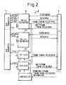
- Fig. 2is a diagram showing the configuration of a low-order channel interface according to one embodiment of the invention.
- the numeral 11is a codec which consists of a digital-to-analog (D/A) converter 12 for converting PCM signals into analog signals, and an analog-to-digital (A/D) converter 13 for converting analog signals into PCM signals.
- D/Adigital-to-analog
- A/Danalog-to-digital
- a channel interface converter (CH-inf) 14 for outgoing linesseparates multiframe-structured data (VFR) transferred from the LT 3 into PCM signals for individual channels by using a clock (MCKR), frame timing pulse (FPR), and multiframe timing pulse (ABR), and transfers data (VFR') to the respective D/A converter units 12 together with a clock (MCKR'), frame timing pulse (FPR'), and multiframe timing pulse (ABR').
- MCKRclock
- FPRframe timing pulse
- ABRmultiframe timing pulse
- a channel interface converter (CH-inf) 15 for incoming linessupplies a clock (MCKS') to the A/D converter 13 for each channel in response to a clock (MCKS) fed from the LT 3, and multiplexes data (VFS'), i.e. PCM signals supplied from the A/D converter 13 in synchronism with the clock (MCKS'), into frame/multiframe-structured data (VFS) which is transferred to the LT 3.
- CH-infmultiplexes data
- MCKS'multiplexes data supplied from the A/D converter 13 in synchronism with the clock (MCKS') into frame/multiframe-structured data (VFS) which is transferred to the LT 3.
- a frame timing generator (FP-GEN) 16performs phase correction on the frame timing pulse (FPR) fed from the LT 3 by using frame timing phase difference information supplied from a controller 18, and produces outputs, one being supplied to the LT 3 as a frame timing pulse (FPS) and the other supplied to the A/D converter 13 as a frame timing pulse (FPS') for each channel.
- FPRframe timing pulse
- FPSframe timing pulse
- FPS'frame timing pulse
- a multiframe timing generator (AB-GEN) 17performs phase correction on the multiframe timing pulse (ABR) fed from the LT 3 by using multiframe timing phase difference information supplied from the controller 18, and produces outputs, one being supplied to the LT 3 as a multiframe timing pulse (ABS) and the other supplied to the A/D converter 13 as a multiframe timing pulse (ABS') for each channel.
- ABRmultiframe timing pulse
- ABSmultiframe timing pulse
- the controller 18supplies the frame timing phase difference information to the FP-GEN 16 and the multiframe phase difference information to the AB-GEN 17 in accordance with frame/multiframe timing phase difference information supplied from the multiplexer 6 (Fig. 3).
- Fig. 3is a diagram showing the configuration of a multiplexer as used in one embodiment of the invention, wherein the same parts as those shown in Fig. 1 are designated by the same numerals.
- the multiplexer 6consists of a demultiplexing unit (DMUX) 21 for demultiplexing a higher-level multiplexed signal, and a multiplexing unit (MUX) 22 for multiplexing lower-level multiplexed signals into a higher-level multiplexed signal.
- the DMUX 21demultiplexes the higher-level multiplexed signal and distributes each of the demultiplexed multiframe data (VFR) to the LT 4 together with a clock (MCKR), frame timing pulse (FPR), and multiframe timing pulse (ABR).
- MCKRclock
- FPRframe timing pulse
- ABRmultiframe timing pulse
- the MUX 22sends a clock (MCKS) to the LT 4 and multiplexes data (VFS) from the LT 4 into a higher-level multiplexed signal for transmission to higher-order equipment.
- MCKSclock
- VFSmultiplexes data
- a frame phase difference detector (FP-DET) 23compares a frame timing pulse (MFPS) fed from the MUX 22 with a frame timing pulse (FPS) fed from the LT 4, and produces frame timing phase difference information.
- a multiframe phase difference detector (AB-DET) 24compares a multiframe timing pulse (MABS) fed from the MUX 22 with a multiframe timing pulse (ABS) fed from the LT 4, and produces multiframe timing phase difference information.
- a controller 25transmits the frame timing phase difference information from the FP-DET 23 and the multiframe timing phase difference information from the AB-DET 24 to the controller 18 (Fig. 2) in the low-order channel interface 2.
- the frame phase difference and the multiframe phase difference occurring between the MUX 22 and the LT 4are detected in the multiplexer 6, and the detected information is transmitted to the low-order channel interface 2, where, based on this information, the phase differences of the frame timing and multiframe timing pulses between the A/D converter 13 and the LT 3 are corrected, compensating for differences in delay time between LT 3 and LT 4 and thus reducing the phase differences of the frame and multiframe signals, respectively, to zero.
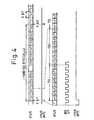
- Fig. 4shows the timing for the various signals in association with the frame structure.
- one frameconsists of 24 time slots (TS), but this is only illustrative and not restrictive.
- VFS/Rindicates frame-structured data for incoming and outgoing lines.
- TS1 to TS24are time slots; each TS consists of 8-bit data, b1 to b8, and a 1-bit framing bit (F) is added at the beginning of the frame, so that each frame consists of a total of 193 bits (in 125 ⁇ s).
- FPS/Ris a frame timing pulse for incoming and outgoing lines
- MFPSis a frame timing pulse output from the multiplexer 6
- MCKS/Ris a clock signal for incoming and outgoing lines.
- Fig. 5shows the timing of the various signals in association with the multiframe structure.
- one multiframeconsists of 12 frames, but this is only illustrative and not restrictive.
- VFS/Rindicates multiframe-structured data for incoming and outgoing lines.
- F1 to F12are frames each corresponding to the 193-bit frame illustrated in Fig. 4.
- ABSis a multiframe timing pulse for incoming lines
- MABSis a multiframe timing pulse output from the multiplexer 6
- ABRis a multiframe timing pulse for outgoing lines
- FPS/Ris a frame timing pulse for incoming and outgoing lines
- MCKS/Ris a clock signal for incoming and outgoing lines.
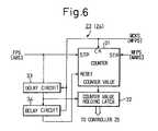
- Fig. 6is a circuit block diagram showing a configurational example of the frame phase difference detector (or multiframe phase difference detector). These detectors can be easily implemented using relatively simple logic circuits.
- the signals associated with the multiframe phase difference detector 24are shown in square brackets along with the corresponding signals associated with the frame phase difference detector 23.
- the numeral 31indicates a counter which counts the number of clock pulses (MCKS) or frame timing pulses (MFPS), starting from the pulse position of the frame timing pulse (MFPS) or multiframe timing pulse (MABS) applied at a start signal input (STR) from the MUX 22 and ending at the pulse position of the frame timing pulse (FPS) or multiframe timing pulse (ABS) applied at a stop signal input (STP) from the LT 4.
- the resulting counter valueis latched into a counter value holding latch 32 before transfer to the controller 25.
- Delay circuits 33 and 34are provided which delay the frame timing pulse (FPS) or multiframe timing pulse (MFPS) in accordance with the clock (MCKS) or frame timing pulse (MFPS), and which produce a latch timing signal for the counter value holding latch 32 and a reset signal for the counter 31, respectively.
- FPSframe timing pulse
- MFPSmultiframe timing pulse
- MCKSclock
- MFPSframe timing pulse
- the counter 31is started by the application of MFPS or MABS, and stopped by the application of FPS or ABS, upon which the counter value is read out. It will be appreciated, however, that the counter value may also be read out by starting the counting upon FPS or ABS and stopping it upon MFPS or MABS.
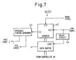
- Fig. 7is a circuit block diagram showing a configurational example of the frame timing generator (multiframe timing generator). These generators also can be easily implemented using relatively simple logic circuits. In the figure, the signals associated with the multiframe timing generator 17 are shown in square brackets along with the corresponding signals associated with the frame timing generator 16.
- the numeral 41indicates a data buffer where the phase correction data from the controller 18 is stored.
- a counter 42is reset by the frame timing pulse (FPR) or multiframe timing pulse (ABR) applied from the LT 3, and counts the number of clock pulses (MCKR) or frame timing pulses (FPR) by a period equal to the phase correction data written in the data buffer 41.
- a signalis output from a carry signal output (CO) whereby an FPS [ABS] timing generator 44 is driven to generate frame timing pulses (FPS, FPS') or multiframe timing pulses (ABS, ABS').
- a delay circuit 43delays FPR or ABR and supplies the resulting output to the data buffer 41 as a loading signal by which the phase correction data is written into the data buffer 41 immediately after the resetting of the counter 42.
- the FPS [ABS] timing generator 44At the completion of the counting by the counter 42, the FPS [ABS] timing generator 44 generates the frame timing pulses (FPS, FPS') or the multiframe timing pulses (ABS, ABS').
- Figs. 8 and 9are flowcharts illustrating the operations of the controllers: Fig. 8 for the controller 25 and Fig. 9 for the controller 18.
- the controller 25reads the frame phase difference data and multiframe phase difference data from the frame phase difference detector 23 and multiframe phase difference detector 24, respectively, and transmits the phase difference data to the controller 18 if the frame phase difference or multiframe phase difference is not zero. Then, after waiting for a prescribed time, the operation returns to the beginning of the control process. The prescribed waiting time is inserted to perform the control in an intermittent manner.
- the controller 18when the phase difference data is received from the controller 25, the controller 18 writes the frame phase difference data into the frame timing generator 16 and the multiframe phase difference data into the multiframe timing generator 17.
- the processing in the controllers 18 and 25is implemented in software, but since the processing is relatively simple, it can also be easily implemented in hardware using logic circuits.
- Communication between the controllers 18 and 25is accomplished, for example, by using overhead bits appended to the data transmitted between the LT 3 and LT 4.
Landscapes
- Engineering & Computer Science (AREA)
- Computer Networks & Wireless Communication (AREA)
- Signal Processing (AREA)
- Time-Division Multiplex Systems (AREA)
- Synchronisation In Digital Transmission Systems (AREA)
Description
- The present invention relates to a method andapparatus for correcting the phase of transmitted dataframes, and more particularly to a method and apparatusfor correcting the phase of frames/multiframestransmitted over incoming lines in subscriber loopcarrier systems.
- Subscriber loop carrier systems have beenemployed to accommodate subscribers, at geographicallyremote locations from switching offices, economically andwith high transmission quality, and also to alleviate theproblem of the ever increasing number of telephone cablesin urban areas. In conventional subscriber loop carriersystems, a plurality of subscriber lines are multiplexedas PCM data with a frame/multiframe structure at a remoteterminal (RT), and the thus multiplexed PCM data are thentransmitted over a fiber optic or other transmissionmedium to a central office terminal (COT), where the dataare demultiplexed into a plurality of subscriber linesfor connection to switching equipment. Furthermore, inrecent years, high-order multiplexing has come to beadopted wherein a plurality of multiplexed data, insteadof undergoing demultiplexing at a COT, are furthermultiplexed into a high-level multiplexed signal, fordirect connection to a switching network such as SONET.To achieve this, a multiplexer for remultiplexing aplurality of multiplexed data is provided with a timeslot interchanger (TSI) for interchanging time slots toaccomplish dynamic rearrangement on a user-by-user basis.The TSI is provided to accommodate a larger number ofsubscriber lines than the number of channels in a multiplexed transmission path. To facilitate theinterchanging of time slots in the TSI, the phases of theframes/multiframes of the PCM data transmitted overdifferent transmission paths from different RTs must becorrected to achieve synchronization. In the prior art,this phase correction is done by storing the data inmemory at the receiving end. This requires the provisionof a memory for storing the data, and furthermore,transmission delays are caused because of temporarilystoring the data.
- If the differences between transmission delaytimes from the different RTs are within one-frame period,the phase correction is only necessary for the frame, butno phase correction is needed for the multiframe. Inthis case, a memory that can store one frame of data willsuffice for the purpose, and the transmission delay canbe kept within one frame period. On the other hand, ifthe differences between transmission delay times from thedifferent RTs are larger than one frame period, the phasecorrection must be done not only for the frame but forthe multiframe that typically consists of 12 frames. Insuch a case, the memory capacity required will be muchlarger, and significant transmission delays will result.Furthermore, in order to use a single fiber optic cablefor carrying both the incoming and outgoing lines, theadoption of a time compression multiplexing (TCM) systemis considered. If the TCM system is adopted, phasecorrection for the multiframe becomes essential.
- In US-A-3 980 835, the oscillator frequency at areceiving end is controlled on the basis of advance (A),retard (R) and out-of-limits (OL) signals from thetransmitting end and A, R and OL signals made at thereceiving end.
- In US-A-5,140,616, at a transmitting end in a local phasedifference indicator indicating a phase relation between afirst data adapter and a first synchronous master istransmitted to a second (remote) data adapter at a receivingend, where a baud clock generator uses the phase differenceindicator to generate a baud clock which is used to transferdata from the second data adapter to a second synchronousmaster. Accordingly, the phase difference is transmitted fromthe transmitting end to the receiving end, and is used at thereceiving end.
- Lastly, reference is made to GB-A-1 577 331, in which theclock frequency of a switching center receiving end iscontrolled based on incoming A-R-Z at a ("advance", "retard"and "do-nothing" signals) transmitted from a switching centerat a transmitting end and the local A-R-Z.
- It is an object of the present invention to provide a methodand apparatus for phase correction in subscriber loop carriersystems, whereby phase correction can be done for frames andmultiframes relying on memory storage.
- According to the present invention from one aspect, there isprovided a frame phase correction method having the featuresof
claim 1. - According to the present invention from another aspect, thereis provided a frame phase correcting apparatus having thefeatures of
claim 6. - The invention will be better understood by referring, by wayof example, to the accompanying drawings, in which:
- Fig. 1 is a block diagram showing the basic configuration ofa subscriber loop carrier system in which an embodiment ofthe present invention is incorporated;
- Fig. 2 is a block diagram showing the configuration of a low-orderchannel interface;
- Fig. 3 is a block diagram showing the configuration of amultiplexer;
- Fig. 4 is a diagram showing the timing for various signals inassociation with a frame structure;
- Fig. 5 is a diagram showing the timing for various signals inassociation with a multiframe structure;
- Fig. 6 is a circuit block diagram showing a configurationalexample of a frame or multiframe phase difference detector;
- Fig. 7 is a circuit block diagram showing aconfigurational example of a frame or multiframe timinggenerator; and
- Figs. 8 and 9 are flowcharts for controllers.
- Fig. 1 is a diagram showing the basic configurationof a subscriber loop carrier system in which an embodiment of thepresent invention is incorporated; the overall configuration of thesystem is shown here in a simplified form. In thefigure, the
numeral 1 designates a subscriber interface(CH), provided for each subscriber, and via which ananalog signal from the subscriber (telephone) side isconverted to a PCM signal for transmission over eachindividual channel and vice versa. A low-order channelinterface (CH inf) 2 is provided via which PCM signalsfrom the individual channels are multiplexed into ordemultiplexed from a multiframe signal. Lineterminations (LT) 3 and 4 each perform conversion betweena multiplexed signal and a signal transmitted or fortransmission over an optical ormetallic transmissionpath 5. Amultiplexer 6 converts the multiplexed signalsinto a higher-level multiplexed signal for connection toa switching network and vice versa. - Fig. 2 is a diagram showing the configuration of alow-order channel interface according to one embodimentof the invention. The same parts as those shown in Fig.1 are designated by the same numerals. In the low-
orderchannel interface 2, thenumeral 11 is a codec whichconsists of a digital-to-analog (D/A)converter 12 forconverting PCM signals into analog signals, and ananalog-to-digital (A/D)converter 13 for convertinganalog signals into PCM signals. - A channel interface converter (CH-inf) 14 foroutgoing lines separates multiframe-structured data (VFR)transferred from the
LT 3 into PCM signals for individualchannels by using a clock (MCKR), frame timing pulse(FPR), and multiframe timing pulse (ABR), and transfers data (VFR') to the respective D/A converter units 12together with a clock (MCKR'), frame timing pulse (FPR'),and multiframe timing pulse (ABR'). - A channel interface converter (CH-inf) 15 forincoming lines supplies a clock (MCKS') to the A/
Dconverter 13 for each channel in response to a clock(MCKS) fed from theLT 3, and multiplexes data (VFS'),i.e. PCM signals supplied from the A/D converter 13 insynchronism with the clock (MCKS'), intoframe/multiframe-structured data (VFS) which istransferred to theLT 3. - A frame timing generator (FP-GEN) 16 performs phasecorrection on the frame timing pulse (FPR) fed from the
LT 3 by using frame timing phase difference informationsupplied from acontroller 18, and produces outputs, onebeing supplied to theLT 3 as a frame timing pulse (FPS)and the other supplied to the A/D converter 13 as a frametiming pulse (FPS') for each channel. - A multiframe timing generator (AB-GEN) 17 performsphase correction on the multiframe timing pulse (ABR) fedfrom the
LT 3 by using multiframe timing phase differenceinformation supplied from thecontroller 18, and producesoutputs, one being supplied to theLT 3 as a multiframetiming pulse (ABS) and the other supplied to the A/Dconverter 13 as a multiframe timing pulse (ABS') for eachchannel. - The
controller 18 supplies the frame timing phasedifference information to the FP-GEN 16 and themultiframe phase difference information to the AB-GEN 17in accordance with frame/multiframe timing phasedifference information supplied from the multiplexer 6(Fig. 3). - Fig. 3 is a diagram showing the configuration of amultiplexer as used in one embodiment of the invention,wherein the same parts as those shown in Fig. 1 aredesignated by the same numerals. The
multiplexer 6consists of a demultiplexing unit (DMUX) 21 for demultiplexing a higher-level multiplexed signal, and amultiplexing unit (MUX) 22 for multiplexing lower-levelmultiplexed signals into a higher-level multiplexedsignal. TheDMUX 21 demultiplexes the higher-levelmultiplexed signal and distributes each of thedemultiplexed multiframe data (VFR) to theLT 4 togetherwith a clock (MCKR), frame timing pulse (FPR), andmultiframe timing pulse (ABR). - The MUX 22 sends a clock (MCKS) to the
LT 4 andmultiplexes data (VFS) from theLT 4 into a higher-levelmultiplexed signal for transmission to higher-orderequipment. - A frame phase difference detector (FP-DET) 23compares a frame timing pulse (MFPS) fed from the
MUX 22with a frame timing pulse (FPS) fed from theLT 4, andproduces frame timing phase difference information. Amultiframe phase difference detector (AB-DET) 24 comparesa multiframe timing pulse (MABS) fed from theMUX 22 witha multiframe timing pulse (ABS) fed from theLT 4, andproduces multiframe timing phase difference information. - A
controller 25 transmits the frame timing phasedifference information from the FP-DET 23 and themultiframe timing phase difference information from theAB-DET 24 to the controller 18 (Fig. 2) in the low-orderchannel interface 2. - Thus, the frame phasedifference and the multiframe phase difference occurringbetween the
MUX 22 and theLT 4 are detected in themultiplexer 6, and the detected information istransmitted to the low-order channel interface 2, where,based on this information, the phase differences of theframe timing and multiframe timing pulses between the A/Dconverter 13 and theLT 3 are corrected, compensating fordifferences in delay time betweenLT 3 andLT 4 and thusreducing the phase differences of the frame andmultiframe signals, respectively, to zero. - Fig. 4 shows the timing for the various signals in association with the frame structure. In the exampleshown, one frame consists of 24 time slots (TS), but thisis only illustrative and not restrictive.
- In the figure, VFS/R indicates frame-structured datafor incoming and outgoing lines. TS1 to TS24 are timeslots; each TS consists of 8-bit data, b1 to b8, and a 1-bitframing bit (F) is added at the beginning of theframe, so that each frame consists of a total of 193 bits(in 125 µs).
- FPS/R is a frame timing pulse for incoming andoutgoing lines, MFPS is a frame timing pulse output fromthe
multiplexer 6, and MCKS/R is a clock signal forincoming and outgoing lines. - Fig. 5 shows the timing of the various signals inassociation with the multiframe structure. In theexample shown, one multiframe consists of 12 frames, butthis is only illustrative and not restrictive.
- In the figure, VFS/R indicates multiframe-structureddata for incoming and outgoing lines. F1 to F12 areframes each corresponding to the 193-bit frameillustrated in Fig. 4.
- ABS is a multiframe timing pulse for incoming lines,MABS is a multiframe timing pulse output from the
multiplexer 6, ABR is a multiframe timing pulse foroutgoing lines, FPS/R is a frame timing pulse forincoming and outgoing lines, and MCKS/R is a clock signalfor incoming and outgoing lines. - Fig. 6 is a circuit block diagram showing aconfigurational example of the frame phase differencedetector (or multiframe phase difference detector).These detectors can be easily implemented usingrelatively simple logic circuits. In the figure, thesignals associated with the multiframe
phase differencedetector 24 are shown in square brackets along with thecorresponding signals associated with the framephasedifference detector 23. - In the frame
phase difference detector 23 or the multiframephase difference detector 24, the numeral 31indicates a counter which counts the number of clockpulses (MCKS) or frame timing pulses (MFPS), startingfrom the pulse position of the frame timing pulse (MFPS)or multiframe timing pulse (MABS) applied at a startsignal input (STR) from theMUX 22 and ending at thepulse position of the frame timing pulse (FPS) ormultiframe timing pulse (ABS) applied at a stop signalinput (STP) from theLT 4. The resulting counter valueis latched into a countervalue holding latch 32 beforetransfer to thecontroller 25. Delaycircuits 33 and 34are provided which delay the frame timing pulse (FPS) ormultiframe timing pulse (MFPS) in accordance with theclock (MCKS) or frame timing pulse (MFPS), and whichproduce a latch timing signal for the countervalueholding latch 32 and a reset signal for thecounter 31,respectively. - In the example shown in Fig. 6, the
counter 31 isstarted by the application of MFPS or MABS, and stoppedby the application of FPS or ABS, upon which the countervalue is read out. It will be appreciated, however, thatthe counter value may also be read out by starting thecounting upon FPS or ABS and stopping it upon MFPS orMABS. - Fig. 7 is a circuit block diagram showing aconfigurational example of the frame timing generator(multiframe timing generator). These generators also canbe easily implemented using relatively simple logiccircuits. In the figure, the signals associated with the
multiframe timing generator 17 are shown in squarebrackets along with the corresponding signals associatedwith theframe timing generator 16. - In the
frame timing generator 16 or themultiframetiming generator 17, the numeral 41 indicates a databuffer where the phase correction data from thecontroller 18 is stored. Acounter 42 is reset by theframe timing pulse (FPR) or multiframe timing pulse (ABR) applied from theLT 3, and counts the number of clockpulses (MCKR) or frame timing pulses (FPR) by a periodequal to the phase correction data written in thedatabuffer 41. When the counting is completed, a signal isoutput from a carry signal output (CO) whereby an FPS[ABS]timing generator 44 is driven to generate frametiming pulses (FPS, FPS') or multiframe timing pulses(ABS, ABS'). - A
delay circuit 43 delays FPR or ABR and suppliesthe resulting output to thedata buffer 41 as a loadingsignal by which the phase correction data is written intothedata buffer 41 immediately after the resetting of thecounter 42. At the completion of the counting by thecounter 42, the FPS [ABS]timing generator 44 generatesthe frame timing pulses (FPS, FPS') or the multiframetiming pulses (ABS, ABS'). - Figs. 8 and 9 are flowcharts illustrating theoperations of the controllers: Fig. 8 for the
controller 25 and Fig. 9 for thecontroller 18. Referring to Fig.8, when the line termination (LT) is in synchronizationand no alarm is issued, thecontroller 25 reads the framephase difference data and multiframe phase differencedata from the framephase difference detector 23 andmultiframephase difference detector 24, respectively,and transmits the phase difference data to thecontroller 18 if the frame phase difference or multiframe phasedifference is not zero. Then, after waiting for aprescribed time, the operation returns to the beginningof the control process. The prescribed waiting time isinserted to perform the control in an intermittentmanner. - Referring to Fig. 9, when the phase difference datais received from the
controller 25, thecontroller 18writes the frame phase difference data into theframetiming generator 16 and the multiframe phase differencedata into themultiframe timing generator 17. - In this embodiment, the processing in the
controllers - Communication between the
controllers LT 3 andLT 4.
Claims (10)
- Frame phase correction method for correcting the phase ofdata frames at a receiving end for the data transmittedto the receiving end from a transmitting end, comprisingthe steps of:a) detecting a phase difference (23) between the phase(FPS) of received frames (FPS) and a reference phase(MFPS) at the receiving end (6); andb) transmitting the detected frame phase difference tothe transmitting side (2);
characterized byc) controlling (16, 18) the phase of frames beingformed at the transmitting end (2) in accordancewith the frame phase difference supplied from thereceiving end (6), whereby phase correction isdone without relying on memory storage. - Method according to Claim 1,characterized in that aprescribed number of successive frames are groupedtogether to form a multiframe (F1-F12) and furthercomprising the steps of:d) detecting a phase difference (24) between the phaseof received multiframes (ABS) and a reference phase(MABS) at the receiving end;e) transmitting the detected multiframe phasedifference to the transmitting end (2); andf) controlling (17, 18) the phase of multiframes beingformed at the transmitting end (2) on the basis ofthe multiframe phase difference.
- Method according to Claim 2,characterized in that theframe phase (FPS) and the multiframe phase (ABS)represent the phases of the frames and multiframes,respectively, on incoming lines in a subscriber loopcarrier system.
- Method according to Claim 3,characterized in that thestep a) includes the substeps of:said step c) includes the substeps of:starting a first counter (31) by either one ofpulses representing said reference phase or saidphase of said received frames, andreading a counter value from said first counter (31)in response to receipt of the other one of thepulses representing said reference phase or saidphase of said received frames,said counter value providing an indication of saidphase difference, andloading said counter value into a second counter(42) by the pulse representing said reference phase,anddetermining the phase of the frames to be formed inaccordance with a count end signal output from saidsecond counter (42).
- Method according to Claim 3,characterized in that thestep d) includes the substep of:that step f) includes the substeps of:starting a counter (31) by either one ofpulses representing the reference phase (MABS) orthe phase (ABS) of the received multiframes, andreading a counter value from the counter (31)by the other one (ABS, MABS) of the pulsesrepresenting the reference phase (MABS) or the phase(ABS) of the received multiframes, the counter valueproviding an indication of the phase difference, andloading the counter value into a further counter (42)by the pulse representing the reference phase, anddetermining the phase of the multiframes (F1-F12) tobe formed in accordance with a count end signaloutput from the further counter (42).
- Frame phase correcting apparatus for correcting the phaseof data frames at a receiving end for the datatransmitted to the receiving end from a transmitting end,comprising:a) means (23) for detecting a phase difference betweenthe phase (FPS) of received frames and a referencephase (MFPS) at the receiving end; andb) means for transmitting the frame phase differencedetected by the frame phase difference detectingmeans (23, 24) to the transmitting end (28);
characterized byc) means (18) for controlling the phase of frames beingformed at the transmitting end (2) in accordancewith the frame phase difference supplied from the receiving end (6), whereby phase correction isdone without relying on memory storage. - Apparatus according to Claim 6,characterized in that aprescribed number of successive frames (F1-F2) aregrouped together to form a multiframe, furthercomprising:means (23) for detecting a phase difference between thephase of received multiframes (ABS) and a reference phase(MABS) at the receiving end;means (5) for transmitting the multiframe phasedifference detected by the multiframe phase detectingmeans (24) to the transmitting end (2, 3); andmeans (18) for controlling the phase of multiframes beingformed at the transmitting end (2, 3) on the basis of themultiframe phase difference.
- Apparatus according to Claim 7,characterized in that theframe phase and the multiframe phase represent the phasesof the frames (T1-T24) and multiframes (F1-F12),respectively, on incoming lines in a subscriber loopcarrier system.
- Apparatus according to Claim 8,characterized in that theframe phase difference detecting means (23, 24) includesa first counter (31) which is started by either one ofpulses representing the reference phase (MFPS, ABS) orthe phase of the received frames (FPS, ABS) and fromwhich a counter value is read out by the other one of the.pulses representing the reference phase or the phase ofthe received frames, and
the frame phase control means (18) includes a secondcounter (42) into which the counter value is loaded bythe pulse representing the reference phase (MFPS, ABS) and which is adapted to output a count end signal, and aframe timing generating means (44) which is adapted tooutput a pulse to determine the phase of the frames to beformed in accordance with the count end signal. - Apparatus according to Claim 9,characterized in that themultiframe phase difference detecting means (24) includesa third counter (31) which is started by either one ofpulses representing the reference phase (MABS) or thephase of the received multiframes (ABS), and from which acounter value is read out by the other one of the pulsesrepresenting the reference phase or the phase of thereceived multiframe, and
the multiframe phase control means includes (18) a fourthcounter (42) into which the counter value is loaded bythe pulse representing the reference phase and which isadapted to output a count end signal, and a multiframetiming generating means (44) which is adapted to output apulse to determine the phase of the multiframes to beformed in accordance with the count end signal.
Applications Claiming Priority (3)
| Application Number | Priority Date | Filing Date | Title |
|---|---|---|---|
| JP223224/93 | 1993-09-08 | ||
| JP5223224AJPH0779209A (en) | 1993-09-08 | 1993-09-08 | Frame / multi-frame phase correction method |
| JP22322493 | 1993-09-08 |
Publications (3)
| Publication Number | Publication Date |
|---|---|
| EP0642238A2 EP0642238A2 (en) | 1995-03-08 |
| EP0642238A3 EP0642238A3 (en) | 1995-09-20 |
| EP0642238B1true EP0642238B1 (en) | 2004-05-12 |
Family
ID=16794743
Family Applications (1)
| Application Number | Title | Priority Date | Filing Date |
|---|---|---|---|
| EP94101411AExpired - LifetimeEP0642238B1 (en) | 1993-09-08 | 1994-01-31 | Method and apparatus for correcting phase of frames in subsriber loop carrier system |
Country Status (4)
| Country | Link |
|---|---|
| US (1) | US5528609A (en) |
| EP (1) | EP0642238B1 (en) |
| JP (1) | JPH0779209A (en) |
| DE (1) | DE69433770T2 (en) |
Families Citing this family (10)
| Publication number | Priority date | Publication date | Assignee | Title |
|---|---|---|---|---|
| JPH08228183A (en)* | 1995-02-20 | 1996-09-03 | Fujitsu Ltd | Signal processing device and signal processing method |
| US5828670A (en)* | 1995-06-06 | 1998-10-27 | Symmetricom, Inc. | Distribution of synchronization in a synchronous optical environment |
| DE19523489A1 (en)* | 1995-06-28 | 1997-01-02 | Sel Alcatel Ag | Method and circuit arrangement for the synchronization of pulse frames in multicellular telecommunications systems |
| GB2324214A (en) | 1997-04-08 | 1998-10-14 | Power X Limited | Synchronising arrangements |
| IL123045A0 (en) | 1998-01-25 | 1998-09-24 | Eci Telecom Ltd | Apparatus and method for digital telephony |
| US6287306B1 (en) | 1998-06-22 | 2001-09-11 | Daig Corporation | Even temperature linear lesion ablation catheter |
| KR100497351B1 (en)* | 2001-02-08 | 2005-06-23 | 삼성전자주식회사 | Apparatus for compensating phase discord according to time division multiplex and method thereof |
| EP1365531B1 (en)* | 2002-05-02 | 2004-10-06 | Alcatel | Method of phase controlling of a data signal, counterpropagating clock circuit arrangement and interface device |
| JP4448076B2 (en)* | 2005-09-16 | 2010-04-07 | 富士通株式会社 | Timing adjustment circuit for data transmission / reception circuit, LSI and data transmission / reception system |
| US20070183462A1 (en) | 2006-02-04 | 2007-08-09 | Daugherty Charles H | Method and apparatus for aligning source data streams in a communications network |
Family Cites Families (9)
| Publication number | Priority date | Publication date | Assignee | Title |
|---|---|---|---|---|
| US3562432A (en)* | 1966-11-16 | 1971-02-09 | Communications Satellite Corp | Synchronizer for time division multiple access satellite communication system |
| GB1508986A (en)* | 1974-05-29 | 1978-04-26 | Post Office | Digital network synchronising system |
| GB1577331A (en)* | 1976-06-19 | 1980-10-22 | Plessey Co Ltd | Synchronisation arrangements for digital switching centres |
| JPS57168545A (en)* | 1981-04-09 | 1982-10-16 | Fujitsu Ltd | Controlling system for frame ttransfer phase |
| JPS6124338A (en)* | 1984-07-12 | 1986-02-03 | Nec Corp | Multi-direction multiplex communication system |
| US5091899A (en)* | 1988-02-04 | 1992-02-25 | Matsushita Electric Industrial Co., Ltd. | Time code recording or reproducing apparatus and time code converter |
| EP0439630B1 (en)* | 1989-08-25 | 1996-02-07 | Nippon Telegraph And Telephone Corporation | Wireless channel switch control method |
| JP2512586B2 (en)* | 1990-03-08 | 1996-07-03 | 富士通株式会社 | Frame synchronization-dependent bit synchronization extraction circuit |
| US5140616A (en)* | 1990-11-19 | 1992-08-18 | Ag Communication Systems Corporation | Network independent clocking circuit which allows a synchronous master to be connected to a circuit switched data adapter |
- 1993
- 1993-09-08JPJP5223224Apatent/JPH0779209A/ennot_activeWithdrawn
- 1994
- 1994-01-31DEDE69433770Tpatent/DE69433770T2/ennot_activeExpired - Lifetime
- 1994-01-31USUS08/189,408patent/US5528609A/ennot_activeExpired - Lifetime
- 1994-01-31EPEP94101411Apatent/EP0642238B1/ennot_activeExpired - Lifetime
Also Published As
| Publication number | Publication date |
|---|---|
| DE69433770T2 (en) | 2005-04-28 |
| EP0642238A3 (en) | 1995-09-20 |
| DE69433770D1 (en) | 2004-06-17 |
| EP0642238A2 (en) | 1995-03-08 |
| JPH0779209A (en) | 1995-03-20 |
| US5528609A (en) | 1996-06-18 |
Similar Documents
| Publication | Publication Date | Title |
|---|---|---|
| US5461622A (en) | Method and apparatus for using SONET overheat to align multiple inverse multiplexed data streams | |
| EP0788695B1 (en) | Method for disassembling and assembling frame structures containing pointers | |
| US6842787B2 (en) | Method and device for converting virtually concatenated data streams into contiguously concatenated data streams | |
| US4143246A (en) | Time division line interface circuit | |
| JPH07170284A (en) | Telecommunication network, its main station and distributing substation | |
| EP0642238B1 (en) | Method and apparatus for correcting phase of frames in subsriber loop carrier system | |
| EP0788694B1 (en) | Method and equipment for elastic buffering in a synchronous digital telecommunication system | |
| US4595907A (en) | PCM data translating apparatus | |
| US4977558A (en) | Demultiplexing device of synchronous multiplexing system | |
| JP3429309B2 (en) | Method and apparatus for monitoring the filling rate of an elastic buffer memory in a synchronous digital telecommunications system | |
| NZ244596A (en) | Synchroniser for asynchronous transfer mode digital network terminal equipment | |
| US4302839A (en) | Multiplex unit with means for responding to signal loss in one or more channels | |
| EP0699363B1 (en) | Method and device for making a justification decision at a node of a synchronous digital telecommunication system | |
| JP3246423B2 (en) | Network synchronization device | |
| GB2285725A (en) | Data burst transfer | |
| US5418788A (en) | Data link terminator | |
| JP3189057B2 (en) | Method and apparatus for transmitting carrier relay signal | |
| EP0136749A1 (en) | Telephone exchange comprising peripheral control domains | |
| HK1011805B (en) | Method and equipment for monitoring the fill rate of an elastic buffer memory in a synchronous digital telecommunication system | |
| JP2001119362A (en) | Control time slot switching circuit | |
| JPH10336131A (en) | Bulk transmission device and bulk transmission method | |
| HK1002378B (en) | Method and equipment for elastic buffering in a synchronous digital telecommunication system | |
| JPH0477137A (en) | Privacy transmission system | |
| HK1002380B (en) | Method for disassembling and assembling frame structures containing pointers |
Legal Events
| Date | Code | Title | Description |
|---|---|---|---|
| PUAI | Public reference made under article 153(3) epc to a published international application that has entered the european phase | Free format text:ORIGINAL CODE: 0009012 | |
| AK | Designated contracting states | Kind code of ref document:A2 Designated state(s):DE FR GB | |
| PUAL | Search report despatched | Free format text:ORIGINAL CODE: 0009013 | |
| AK | Designated contracting states | Kind code of ref document:A3 Designated state(s):DE FR GB | |
| 17P | Request for examination filed | Effective date:19960318 | |
| 17Q | First examination report despatched | Effective date:19980427 | |
| GRAP | Despatch of communication of intention to grant a patent | Free format text:ORIGINAL CODE: EPIDOSNIGR1 | |
| RIC1 | Information provided on ipc code assigned before grant | Ipc:7H 04Q 11/04 B Ipc:7H 04J 3/12 B Ipc:7H 04L 7/00 B Ipc:7H 04J 3/06 A | |
| GRAA | (expected) grant | Free format text:ORIGINAL CODE: 0009210 | |
| GRAS | Grant fee paid | Free format text:ORIGINAL CODE: EPIDOSNIGR3 | |
| AK | Designated contracting states | Kind code of ref document:B1 Designated state(s):DE FR GB | |
| REG | Reference to a national code | Ref country code:GB Ref legal event code:FG4D | |
| REF | Corresponds to: | Ref document number:69433770 Country of ref document:DE Date of ref document:20040617 Kind code of ref document:P | |
| ET | Fr: translation filed | ||
| PLBE | No opposition filed within time limit | Free format text:ORIGINAL CODE: 0009261 | |
| STAA | Information on the status of an ep patent application or granted ep patent | Free format text:STATUS: NO OPPOSITION FILED WITHIN TIME LIMIT | |
| 26N | No opposition filed | Effective date:20050215 | |
| PGFP | Annual fee paid to national office [announced via postgrant information from national office to epo] | Ref country code:FR Payment date:20100208 Year of fee payment:17 | |
| PGFP | Annual fee paid to national office [announced via postgrant information from national office to epo] | Ref country code:GB Payment date:20100202 Year of fee payment:17 Ref country code:DE Payment date:20100211 Year of fee payment:17 | |
| GBPC | Gb: european patent ceased through non-payment of renewal fee | Effective date:20110131 | |
| REG | Reference to a national code | Ref country code:FR Ref legal event code:ST Effective date:20110930 | |
| PG25 | Lapsed in a contracting state [announced via postgrant information from national office to epo] | Ref country code:FR Free format text:LAPSE BECAUSE OF NON-PAYMENT OF DUE FEES Effective date:20110131 | |
| PG25 | Lapsed in a contracting state [announced via postgrant information from national office to epo] | Ref country code:GB Free format text:LAPSE BECAUSE OF NON-PAYMENT OF DUE FEES Effective date:20110131 | |
| REG | Reference to a national code | Ref country code:DE Ref legal event code:R119 Ref document number:69433770 Country of ref document:DE Effective date:20110802 | |
| PG25 | Lapsed in a contracting state [announced via postgrant information from national office to epo] | Ref country code:DE Free format text:LAPSE BECAUSE OF NON-PAYMENT OF DUE FEES Effective date:20110802 |