EP0637402B1 - Method of making a dual-poly non-volatile memory device using a third polysilicon layer - Google Patents
Method of making a dual-poly non-volatile memory device using a third polysilicon layerDownload PDFInfo
- Publication number
- EP0637402B1 EP0637402B1EP94910657AEP94910657AEP0637402B1EP 0637402 B1EP0637402 B1EP 0637402B1EP 94910657 AEP94910657 AEP 94910657AEP 94910657 AEP94910657 AEP 94910657AEP 0637402 B1EP0637402 B1EP 0637402B1
- Authority
- EP
- European Patent Office
- Prior art keywords
- transistor
- forming
- polysilicon
- volatile
- floating gate
- Prior art date
- Legal status (The legal status is an assumption and is not a legal conclusion. Google has not performed a legal analysis and makes no representation as to the accuracy of the status listed.)
- Expired - Lifetime
Links
- 229910021420polycrystalline siliconInorganic materials0.000titleclaimsabstractdescription39
- 229920005591polysiliconPolymers0.000titleclaimsabstractdescription39
- 238000004519manufacturing processMethods0.000titledescription9
- 239000000758substrateSubstances0.000claimsabstractdescription26
- 238000000034methodMethods0.000claimsabstractdescription17
- 239000004065semiconductorSubstances0.000claimsabstractdescription12
- 230000015654memoryEffects0.000claimsabstractdescription9
- 239000002019doping agentSubstances0.000claimsdescription4
- 239000011253protective coatingSubstances0.000claimsdescription3
- 230000008878couplingEffects0.000claims5
- 238000010168coupling processMethods0.000claims5
- 238000005859coupling reactionMethods0.000claims5
- 230000015572biosynthetic processEffects0.000abstractdescription13
- 238000007254oxidation reactionMethods0.000abstractdescription11
- 238000005457optimizationMethods0.000abstractdescription5
- 238000005530etchingMethods0.000abstractdescription2
- 230000009977dual effectEffects0.000abstract1
- XUIMIQQOPSSXEZ-UHFFFAOYSA-NSiliconChemical compound[Si]XUIMIQQOPSSXEZ-UHFFFAOYSA-N0.000description9
- 229910052710siliconInorganic materials0.000description9
- 239000010703siliconSubstances0.000description9
- 239000007943implantSubstances0.000description5
- 230000015556catabolic processEffects0.000description4
- 238000000151depositionMethods0.000description3
- 230000010354integrationEffects0.000description3
- 230000003647oxidationEffects0.000description3
- 238000006731degradation reactionMethods0.000description2
- 230000008021depositionEffects0.000description2
- 238000010586diagramMethods0.000description2
- 238000009792diffusion processMethods0.000description2
- 230000002411adverseEffects0.000description1
- 230000009286beneficial effectEffects0.000description1
- 239000002784hot electronSubstances0.000description1
- BHEPBYXIRTUNPN-UHFFFAOYSA-Nhydridophosphorus(.) (triplet)Chemical compound[PH]BHEPBYXIRTUNPN-UHFFFAOYSA-N0.000description1
- 230000014759maintenance of locationEffects0.000description1
- 239000000463materialSubstances0.000description1
- 239000002184metalSubstances0.000description1
Images


Classifications
- H—ELECTRICITY
- H10—SEMICONDUCTOR DEVICES; ELECTRIC SOLID-STATE DEVICES NOT OTHERWISE PROVIDED FOR
- H10B—ELECTRONIC MEMORY DEVICES
- H10B41/00—Electrically erasable-and-programmable ROM [EEPROM] devices comprising floating gates
- H10B41/30—Electrically erasable-and-programmable ROM [EEPROM] devices comprising floating gates characterised by the memory core region
- H—ELECTRICITY
- H10—SEMICONDUCTOR DEVICES; ELECTRIC SOLID-STATE DEVICES NOT OTHERWISE PROVIDED FOR
- H10B—ELECTRONIC MEMORY DEVICES
- H10B41/00—Electrically erasable-and-programmable ROM [EEPROM] devices comprising floating gates
- H—ELECTRICITY
- H10—SEMICONDUCTOR DEVICES; ELECTRIC SOLID-STATE DEVICES NOT OTHERWISE PROVIDED FOR
- H10B—ELECTRONIC MEMORY DEVICES
- H10B41/00—Electrically erasable-and-programmable ROM [EEPROM] devices comprising floating gates
- H10B41/40—Electrically erasable-and-programmable ROM [EEPROM] devices comprising floating gates characterised by the peripheral circuit region
- H10B41/42—Simultaneous manufacture of periphery and memory cells
- H—ELECTRICITY
- H10—SEMICONDUCTOR DEVICES; ELECTRIC SOLID-STATE DEVICES NOT OTHERWISE PROVIDED FOR
- H10D—INORGANIC ELECTRIC SEMICONDUCTOR DEVICES
- H10D84/00—Integrated devices formed in or on semiconductor substrates that comprise only semiconducting layers, e.g. on Si wafers or on GaAs-on-Si wafers
- H10D84/90—Masterslice integrated circuits
- H10D84/903—Masterslice integrated circuits comprising field effect technology
- H10D84/907—CMOS gate arrays
- H—ELECTRICITY
- H01—ELECTRIC ELEMENTS
- H01L—SEMICONDUCTOR DEVICES NOT COVERED BY CLASS H10
- H01L2924/00—Indexing scheme for arrangements or methods for connecting or disconnecting semiconductor or solid-state bodies as covered by H01L24/00
- H01L2924/10—Details of semiconductor or other solid state devices to be connected
- H01L2924/11—Device type
- H01L2924/14—Integrated circuits
- H01L2924/143—Digital devices
- H01L2924/1434—Memory
- H01L2924/145—Read-only memory [ROM]
- H01L2924/1451—EPROM
Definitions
- the present inventionpertains to semiconductor devices. Specifically, the present invention pertains to the integration of submicron CMOS devices with non-volatile memory devices.
- EPROMsErasable programmable read only memories
- EEPROMselectrically erasable programmable read only memories
- floating gate devicesof the art.
- these double layer polysilicon non-volatile memory devicesare programmed and accessed using a separate device which is electrically coupled to the memory device.
- programming and accessinghas been accomplished using a transistor formed during the formation of the memory device. That is, the formation of the transistor was incorporated into the manufacturing process flow of the memory device. Specifically, as the second layer of polysilicon was deposited to form the memory cell, the polysilicon was also deposited onto a separate region of the substrate. A transistor was then formed in that separate region having the second layer of polysilicon as one of the gates of the device. Incorporating the formation of the transistor into the manufacturing process flow was considered to be advantageous in that it simplified the manufacturing processes required in the formation of the devices.
- Floating gate devicessuch as EPROMs and EEPROMs, require significant oxidation after the deposition of each of the polysilicon layers forming these devices. Multiple poly re-oxidations are necessary to achieve adequate charge retention characteristics.
- submicron CMOS devicesexperience significant transconductance and reliability degradation when exposed to excessive poly re-oxidation. As a result, performance of submicron CMOS devices exposed to dual-poly formation processes is prohibitively reduced. Specifically, as submicron polysilicon gates are exposed to repeated oxidation, the edges of the gates tend to lift from the substrate due to oxidation of the gate edges. This decouples the gate from the channel region. As a result, gain degradation and hot electron reliability problems occur. Additionally, the re-oxidation thermal cycle causes dopant diffusion of the channel's voltage adjust implant.
- dual-poly non-volatile memory devicesis often incompatible with the use of high performance submicron CMOS devices.
- EPROMs and EEPROMsfrequently require relatively high programming voltages of 12-18 volts. Such voltages are incompatible with thin gate oxides and lower diode breakdowns found in submicron CMOS devices.
- Submicron CMOS devicestypically have thin gate oxide thicknesses of less than 20 nm (200 angstroms). A gate oxide of less than 20 nm (200 angstroms) however, has an intrinsic breakdown of approximately 15 volts. Therefore, the programming voltages utilized in dual-poly non-volatile memory elements essentially destroy high performance submicron CMOS devices.
- This objecthas been achieved by the method of claim 1 comprising the steps of depositing a third layer of polysilicon associated with a non-volatile memory device as one of the gates of a high performance submicron CMOS device. This is done in a manner which decouples the processing for the high performance CMOS device from the processing for the non-volatile memory device allowing for separate optimization of the two device types.
- a thin gate oxideis formed over the active area, and a threshold voltage adjust implant is performed.
- a third layer of polysiliconis then deposited over the non-volatile memory device and the surface of the semiconductor substrate.
- the third layer of polysiliconis doped and selectively removed from the surface of the semiconductor substrate such that doped layer of polysilicon is removed from everywhere on the substrate except for the active region where the submicron device gates are to be formed.
- a high performance submicron CMOS device having a source, drain and gate,is then formed using the portion of the doped polysilicon layer remaining in the active region as a gate.
- Metallized contactsare made to the submicron CMOS device, and the device is covered with a protective coating.
- the devicesare formed at separate times, separate optimization of dual-poly non-volatile memory devices and high performance submicron CMOS devices is possible. Additionally, the present invention allows the submicron CMOS device to be decoupled from the source and drain diffusion cycles required to achieve higher junction breakthrough voltages in non-volatile memory devices. Furthermore, the separate optimization can be achieved without compromising the characteristics or reliability of either of the devices.
- FIG. 1Aa cross-sectional view of the starting step in the formation of the present invention is shown.
- a p-doped silicon substrate 20 containing a p-doped well 22 and having an EPROM 24 formed thereonis shown.
- the semiconductor substrate 20is formed of silicon in the preferred embodiment, any other suitable semiconductor material may be used. Additionally, the substrate 20 may also have a different conductivity type if desired. Further, although an EPROM 24 is used in the preferred embodiment, an EEPROM is also compatible with the methods of the present invention.
- the EPROM 24is formed of two stacked and aligned layers of polysilicon, 26 and 28, formed over a high voltage source 30 and drain 32.
- the two layers of polysilicon, 26 and 28,are separated by an insulating dielectric layer 34, and are subjected to re-oxidation.
- a layer of thermal oxide 36is formed over the EPROM 24 and the silicon substrate 20.
- the thermal oxide 36is formed to a depth of approximately 20 nm (200 angstroms).
- the thermal oxide layer 36is then removed from a region 38 of the silicon substrate 20 above the p-doped well 22. In so doing, the thermal oxide 36 is cleared from the active region 38 of the silicon substrate 20 where the thin gate oxide layer of the high performance submicron CMOS transistor is to be formed. In the preferred embodiment, the thermal oxide 36 is removed using a wet HF etch, however, any of the numerous etching techniques well known in the art are suitable.
- a thin gate oxide layer 40is formed in the active region 38 of the silicon substrate 20.
- the gate oxide 40is typically formed to a thickness of approximately 10 to 15 nm (100 to 150 angstroms).
- additional re-oxidationalso occurs in the two polysilicon layers, 26 and 28, of the EPROM 24.
- the polysilicon layers, 26 and 28,are oxidized to a final thickness of about 50 nm (500 angstroms).
- an enhancement implant 42is made into the p-doped region 22 of the silicon substrate 20.
- Enhancement implant 42is a light dose implant of BF 2 , or any other well known dopant, which is used to adjust the threshold voltage of the high performance submicron CMOS transistor.
- a third layer of polysilicon 44is deposited over the surface of the silicon substrate. As a result, both the thin gate oxide 40 and the EPROM 24 are covered by the layer of polysilicon 44.
- the polysilicon 44is typically deposited to a thickness of about 200 to 500 nm (2000 to 5000 angstroms).
- the third layer of polysilicon 44is then doped with an n-type dopant such as phosphorous, producing an n + type conductivity in the third polysilicon layer 44.
- the third doped layer of polysilicon 44is then removed from everywhere on the silicon substrate 20 except for the area above the thin gate oxide 40. In so doing, a gate region 46 for the high performance submicron CMOS transistor is formed.
- the submicron CMOS deviceis effectively decoupled from the EPROM device 24, allowing for separate optimization of the two devices. As a result, the transistor is not adversely affected by the high programming voltages, 12-20 volts, necessary for the EPROM 24.
- An additional etch stepis then performed in order to remove any residual polysilicon that may have been deposited onto the sidewalls of the first two polysilicon layers, 26 and 28, during the deposition of the submicron third polysilicon layer 44.
- the formation of the submicron CMOS transistoris completed by implanting a low voltage source 48 and drain 50, and forming metallized contacts, not shown, to low voltage source 48 and drain 50, and gate 46. The device is then covered with a protective coating.
- an N-channel type high performance submicron CMOS transistoris formed.
- the methods of the present inventionwould also apply to the formation of a P-channel type high performance submicron transistor, by forming the transistor in an n-doped well containing a p-doped source and drain region.
- a circuit diagram illustrating the integration of the submicron CMOS device and EPROM 24 of the present inventionis shown.
- EPROM 24 and high performance sub-micron CMOS transistor 60used to access EPROM 24, are coupled in series between column line 62 and ground line 64.
- the drain terminal of submicron CMOS transistor 60is connected to column line 62 through metal contact 66.
- the gate of transistor 60is coupled to access line 68.
- the gate of EPROM 24is coupled to a read line 70.
- high speed submicron CMOS transistor 60may be used to access EPROM 24.
- the third polysilicon layer 44allows the high performance submicron CMOS transistor to be formed without having to be subjected to the significant re-oxidations required in the formation of the EPROM 24.
- the EPROMcan be accessed and read at higher speeds than were possible with the standard transistors of the prior art. Additionally, the third layer of polysilicon 44 decouples the submicron CMOS transistor and the EPROM 24 such that they may be separately optimized. As a result, both of the devices can be utilized without compromising the characteristics or reliability of the other.
- the two devicescan be manufactured in the same process flow, thereby reducing the manufacturing cost of the system, by eliminating manufacturing steps, while simultaneously improving the yield and reliability of the manufacturing processes.
Landscapes
- Engineering & Computer Science (AREA)
- Manufacturing & Machinery (AREA)
- Non-Volatile Memory (AREA)
- Semiconductor Memories (AREA)
Abstract
Description
- The present invention pertains to semiconductordevices. Specifically, the present invention pertainsto the integration of submicron CMOS devices withnon-volatile memory devices.
- Erasable programmable read only memories, knownas EPROMs, and electrically erasable programmable readonly memories, known as EEPROMs, are well known "floatinggate" devices of the art. Typically, these double layerpolysilicon non-volatile memory devices are programmedand accessed using a separate device which is electricallycoupled to the memory device. In the past, such programmingand accessing has been accomplished using atransistor formed during the formation of the memory device.That is, the formation of the transistor was incorporatedinto the manufacturing process flow of thememory device. Specifically, as the second layer ofpolysilicon was deposited to form the memory cell, thepolysilicon was also deposited onto a separate region ofthe substrate. A transistor was then formed in thatseparate region having the second layer of polysilicon asone of the gates of the device. Incorporating the formationof the transistor into the manufacturing processflow was considered to be advantageous in that it simplifiedthe manufacturing processes required in the formationof the devices.
- Accessing the floating gate device using a highperformance submicron CMOS transistor would be especiallybeneficial due to the high speed at which the submicronCMOS device operates. However, several incompatibilities exist which inhibit integrating the formation of submicronCMOS devices, such as high performance N-channel andP-channel transistors, with the manufacturing processesused to form double layer polysilicon non-volatile memorydevices such as EPROMs and EEPROMs.
- Floating gate devices, such as EPROMs and EEPROMs,require significant oxidation after the depositionof each of the polysilicon layers forming these devices.Multiple poly re-oxidations are necessary to achieve adequatecharge retention characteristics. Unfortunately,submicron CMOS devices experience significant transconductanceand reliability degradation when exposed to excessivepoly re-oxidation. As a result, performance ofsubmicron CMOS devices exposed to dual-poly formationprocesses is prohibitively reduced. Specifically, assubmicron polysilicon gates are exposed to repeated oxidation,the edges of the gates tend to lift from the substratedue to oxidation of the gate edges. This decouplesthe gate from the channel region. As a result, gaindegradation and hot electron reliability problems occur.Additionally, the re-oxidation thermal cycle causes dopantdiffusion of the channel's voltage adjust implant.
- Furthermore, the operation of dual-poly non-volatilememory devices is often incompatible with theuse of high performance submicron CMOS devices. EPROMsand EEPROMs frequently require relatively high programmingvoltages of 12-18 volts. Such voltages are incompatiblewith thin gate oxides and lower diode breakdownsfound in submicron CMOS devices. Submicron CMOS devicestypically have thin gate oxide thicknesses of less than 20 nm(200 angstroms). A gate oxide of less than 20 nm (200 angstroms)however, has an intrinsic breakdown of approximately 15volts. Therefore, the programming voltages utilized indual-poly non-volatile memory elements essentially destroyhigh performance submicron CMOS devices.
- In JP-A-43 48072 (which is of the same patent family asUS-A-5 188 976) a semiconductor substrate isdevided in two areas, a first memory array area whereone-transistor memory cells are constructed and a secondperiphery area where the logic and support circuitry foraccessing the memory array are constructed.
- It is an object of the presentinvention to successfully integrate the formation anduse of high performance submicron CMOS devices with the manufacture and operation of dual-poly non-volatilememory devices.
- This object has been achieved bythe method of
claim 1 comprising the steps of depositing athird layer of polysilicon associated with a non-volatilememory device as one of the gates of a high performancesubmicron CMOS device. This is done in a manner whichdecouples the processing for the high performance CMOSdevice from the processing for the non-volatile memorydevice allowing for separate optimization of the twodevice types. We form a layer of thermal oxide over adual-poly non-volatile memory device and over the portionof the surface of the semiconductor substrate on whichthe high performance CMOS device is to be formed. Thethermal oxide is then removed from the active area on thesubstrate where the high performance submicron CMOSdevice is to be formed. - A thin gate oxide is formed over the activearea, and a threshold voltage adjust implant is performed.A third layer of polysilicon is then depositedover the non-volatile memory device and the surface ofthe semiconductor substrate. The third layer of polysiliconis doped and selectively removed from the surface ofthe semiconductor substrate such that doped layer ofpolysilicon is removed from everywhere on the substrateexcept for the active region where the submicron devicegates are to be formed.
- A high performance submicron CMOS device havinga source, drain and gate, is then formed using the portionof the doped polysilicon layer remaining in the activeregion as a gate. Metallized contacts are made tothe submicron CMOS device, and the device is covered witha protective coating.
- Because the devices are formed at separatetimes, separate optimization of dual-poly non-volatilememory devices and high performance submicron CMOS devicesis possible. Additionally, the present invention allows the submicron CMOS device to be decoupled from thesource and drain diffusion cycles required to achievehigher junction breakthrough voltages in non-volatilememory devices. Furthermore, the separate optimizationcan be achieved without compromising the characteristicsor reliability of either of the devices.
- Figs. 1A-E are side sectional views of thesteps used in the integration of the high performancesubmicron CMOS device and the dual-poly non-volatilememory device in accord with the present invention.
- Fig. 2 is a circuit diagram of the integratedhigh performance submicron CMOS device and the dual-polynon-volatile memory device in accord with the presentinvention.
- With reference to Fig. 1A, a cross-sectionalview of the starting step in the formation of the presentinvention is shown. A p-doped
silicon substrate 20 containinga p-doped well 22 and having anEPROM 24 formedthereon is shown. Although thesemiconductor substrate 20 is formed of silicon in the preferred embodiment, anyother suitable semiconductor material may be used. Additionally,thesubstrate 20 may also have a different conductivitytype if desired. Further, although an EPROM 24is used in the preferred embodiment, an EEPROM is alsocompatible with the methods of the present invention. - The EPROM 24 is formed of two stacked andaligned layers of polysilicon, 26 and 28, formed over a
high voltage source 30 anddrain 32. The two layers ofpolysilicon, 26 and 28, are separated by an insulatingdielectric layer 34, and are subjected to re-oxidation.After re-oxidation of the two polysilicon layers, 26 and28, a layer ofthermal oxide 36 is formed over theEPROM 24 and thesilicon substrate 20. In the preferred embodiment of the present invention, thethermal oxide 36is formed to a depth of approximately 20 nm (200 angstroms). - As shown in Fig. 1B, the
thermal oxide layer 36is then removed from aregion 38 of thesilicon substrate 20 above the p-doped well 22. In so doing, thethermaloxide 36 is cleared from theactive region 38 of thesiliconsubstrate 20 where the thin gate oxide layer of thehigh performance submicron CMOS transistor is to beformed. In the preferred embodiment, thethermal oxide 36 is removed using a wet HF etch, however, any of thenumerous etching techniques well known in the art aresuitable. - Referring now to Fig. 1C, a thin
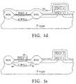
gate oxidelayer 40 is formed in theactive region 38 of thesiliconsubstrate 20. Thegate oxide 40 is typically formed to athickness of approximately 10 to 15 nm (100 to 150 angstroms). Informing thethin gate oxide 40, additional re-oxidationalso occurs in the two polysilicon layers, 26 and 28, oftheEPROM 24. As a result the polysilicon layers, 26 and28, are oxidized to a final thickness of about 50 nm (500 angstroms).After the formation of thethin gate oxide 40,anenhancement implant 42 is made into the p-dopedregion 22 of thesilicon substrate 20.Enhancement implant 42is a light dose implant of BF2, or any other well knowndopant, which is used to adjust the threshold voltage ofthe high performance submicron CMOS transistor. - With reference to Fig. 1D, a third layer of
polysilicon 44 is deposited over the surface of the siliconsubstrate. As a result, both thethin gate oxide 40and theEPROM 24 are covered by the layer ofpolysilicon 44. Thepolysilicon 44 is typically deposited to athickness of about 200 to 500 nm (2000 to 5000 angstroms). The thirdlayer ofpolysilicon 44 is then doped with an n-type dopantsuch as phosphorous, producing an n+ type conductivityin thethird polysilicon layer 44. - As shown in Fig. 1E, the third doped layer of
polysilicon 44 is then removed from everywhere on thesilicon substrate 20 except for the area above thethin gate oxide 40. In so doing, agate region 46 for thehigh performance submicron CMOS transistor is formed. Informinggate 46 of the high performance submicron CMOStransistor fromthird polysilicon layer 44, the submicronCMOS device is effectively decoupled from theEPROM device 24, allowing for separate optimization of the twodevices. As a result, the transistor is not adverselyaffected by the high programming voltages, 12-20 volts,necessary for theEPROM 24. An additional etch step isthen performed in order to remove any residual polysiliconthat may have been deposited onto the sidewalls ofthe first two polysilicon layers, 26 and 28, during thedeposition of the submicronthird polysilicon layer 44. - The formation of the submicron CMOS transistoris completed by implanting a
low voltage source 48 anddrain 50, and forming metallized contacts, not shown, tolow voltage source 48 anddrain 50, andgate 46. Thedevice is then covered with a protective coating. In thepreferred embodiment of the present invention, an N-channeltype high performance submicron CMOS transistor isformed. However, the methods of the present inventionwould also apply to the formation of a P-channel typehigh performance submicron transistor, by forming thetransistor in an n-doped well containing a p-doped sourceand drain region. - Referring now to Fig. 2, a circuit diagram illustratingthe integration of the submicron CMOS deviceand
EPROM 24 of the present invention is shown.EPROM 24and high performancesub-micron CMOS transistor 60, usedto accessEPROM 24, are coupled in series betweencolumnline 62 andground line 64. The drain terminal ofsubmicronCMOS transistor 60 is connected tocolumn line 62throughmetal contact 66. The gate oftransistor 60 iscoupled to accessline 68. Additionally, the gate ofEPROM 24 is coupled to a readline 70. In so doing, highspeedsubmicron CMOS transistor 60, may be used to accessEPROM 24. - Referring again to Fig. 1, the present inventionas described above has several advantages over theprior art. The
third polysilicon layer 44 allows thehigh performance submicron CMOS transistor to be formedwithout having to be subjected to the significant re-oxidationsrequired in the formation of theEPROM 24. - By using a submicron CMOS transistor, the EPROMcan be accessed and read at higher speeds than were possiblewith the standard transistors of the prior art.Additionally, the third layer of
polysilicon 44 decouplesthe submicron CMOS transistor and theEPROM 24 such thatthey may be separately optimized. As a result, both ofthe devices can be utilized without compromising thecharacteristics or reliability of the other. - Additionally, the two devices can be manufacturedin the same process flow, thereby reducing the manufacturingcost of the system, by eliminating manufacturingsteps, while simultaneously improving the yield andreliability of the manufacturing processes.
Claims (8)
- A method of forming a submicron (MOS transistor (60)adjacent to a floating gate non-volatile transistor (24),said method comprising the following sequence of steps:providing a semiconductor substrate (20) of a firstconductivity type,forming said floating gate non-volatile transistor(24) on a first region of said semiconductor substrate(20), including forming a pair of aligned polysiliconlayers (26, 28) separated by an insulating dielectric layer(34) over a high voltage source (30) and drain (32),forming a thermal oxide layer (36) over said floatinggate non-volatile transistor and said semiconductorsubstrate (20),completely removing said thermal oxide (36) from asecond region (38) of said substrate (20) such that thesurface of said second region (38) is left bare, saidsecond region (38) separated from said first region by afield oxide region,forming a gate oxide layer (40) over said secondregion (38) of said substrate (20),forming a third layer of polysilicon (44) over saidfloating gate non-volatile transistor (24) and said thirdgate oxide layer,selectively removing said third layer (44) ofpolysilicon such that said third layer (44) of polysiliconis removed from everywhere except for atop a portion (46)of said second region (38),forming a submicron CMOS transistor (60), includingimplanting dopants of said second conductivity type intosaid second region (38) of said substrate (20) adjacent to andunder said portion (46) of said third layer (44) of polysilicon,forming metallized contacts to said submicron CMOStransistor (60) and said floating gate non-volatiletransistor (24),coupling the drain of said floating gate non-volatiletransistor (24) to the source of said CMOS transistor (60),coupling the source of said non-volatile transistor (24) toa ground potential (64), coupling the drain of said CMOStransistor to a bitline (62), coupling the control gate ofsaid CMOS transistor to an access line (68), coupling thecontrol gate of said non-volatile memory transistor (24) toa read line (70), andcovering said semiconductor substrate (20) includingsaid submicron CMOS transistor (60) and said floating gatenon-volatile transistor (24) with a protective coating.
- The method as recited in claim 1, further comprisingre-oxidizing said pair of polysilicon gates (26, 28), prior toforming said thermal oxide layer (36) over said floatinggate non-volatile transistor (24).
- The method as recited in claim 1, wherein forming saidfloating gate non-volatile transistor (24) furthercomprises the steps of forming an EPROM transistor.
- The method as recited in claim 1, wherein forming saidfloating gate non-volatile transistor (24) furthercomprises the steps of forming an EEPROM transistor.
- The method as recited in claim 1, wherein forming saidsubmicron CMOS transistor (60) comprises the steps offorming a submicron CMOS N-channel transistor.
- The method as recited in claim 1, wherein forming saidsubmicron CMOS transistor (60) comprises the steps offorming a submicron CMOS P-channel transistor.
- The method as recited in claim 1, wherein said gateoxide layer (40) is formed to a depth of between 10 and 15nm.
- The method as recited in claim 1, further includingforming a plurality of said floating gate non-volatile transistorsand a plurality of said submicron CMOS transistors.
Applications Claiming Priority (3)
| Application Number | Priority Date | Filing Date | Title |
|---|---|---|---|
| US08/020,291US5340764A (en) | 1993-02-19 | 1993-02-19 | Integration of high performance submicron CMOS and dual-poly non-volatile memory devices using a third polysilicon layer |
| PCT/US1994/000890WO1994019823A1 (en) | 1993-02-19 | 1994-01-26 | Method of making a dual-poly non-volatile memory device using a third polysilicon layer |
| US20291 | 2001-12-14 |
Publications (3)
| Publication Number | Publication Date |
|---|---|
| EP0637402A1 EP0637402A1 (en) | 1995-02-08 |
| EP0637402A4 EP0637402A4 (en) | 1995-07-19 |
| EP0637402B1true EP0637402B1 (en) | 2000-09-06 |
Family
ID=21797787
Family Applications (1)
| Application Number | Title | Priority Date | Filing Date |
|---|---|---|---|
| EP94910657AExpired - LifetimeEP0637402B1 (en) | 1993-02-19 | 1994-01-26 | Method of making a dual-poly non-volatile memory device using a third polysilicon layer |
Country Status (6)
| Country | Link |
|---|---|
| US (2) | US5340764A (en) |
| EP (1) | EP0637402B1 (en) |
| JP (1) | JP3563403B2 (en) |
| KR (1) | KR100284107B1 (en) |
| DE (1) | DE69425797T2 (en) |
| WO (1) | WO1994019823A1 (en) |
Families Citing this family (13)
| Publication number | Priority date | Publication date | Assignee | Title |
|---|---|---|---|---|
| DE69528971D1 (en)* | 1995-06-30 | 2003-01-09 | St Microelectronics Srl | Method of manufacturing a circuit containing non-volatile memory cells and edge transistors of at least two different types, and corresponding IC |
| DE19614010C2 (en)* | 1996-04-09 | 2002-09-19 | Infineon Technologies Ag | Semiconductor component with adjustable current amplification based on a tunnel current controlled avalanche breakdown and method for its production |
| US5937310A (en)* | 1996-04-29 | 1999-08-10 | Advanced Micro Devices, Inc. | Reduced bird's beak field oxidation process using nitrogen implanted into active region |
| US5882993A (en)* | 1996-08-19 | 1999-03-16 | Advanced Micro Devices, Inc. | Integrated circuit with differing gate oxide thickness and process for making same |
| US6033943A (en)* | 1996-08-23 | 2000-03-07 | Advanced Micro Devices, Inc. | Dual gate oxide thickness integrated circuit and process for making same |
| JPH10247725A (en) | 1997-03-05 | 1998-09-14 | Mitsubishi Electric Corp | Semiconductor device and manufacturing method thereof |
| US5872376A (en)* | 1997-03-06 | 1999-02-16 | Advanced Micro Devices, Inc. | Oxide formation technique using thin film silicon deposition |
| US5962914A (en)* | 1998-01-14 | 1999-10-05 | Advanced Micro Devices, Inc. | Reduced bird's beak field oxidation process using nitrogen implanted into active region |
| KR100258881B1 (en)* | 1998-02-27 | 2000-06-15 | 김영환 | Method for manufacturing semiconductor device |
| US6531364B1 (en) | 1998-08-05 | 2003-03-11 | Advanced Micro Devices, Inc. | Advanced fabrication technique to form ultra thin gate dielectric using a sacrificial polysilicon seed layer |
| TW449919B (en) | 1998-12-18 | 2001-08-11 | Koninkl Philips Electronics Nv | A method of manufacturing a semiconductor device |
| EP1107309B1 (en)* | 1999-12-06 | 2010-10-13 | STMicroelectronics Srl | Manufacturing process for non-volatile floating gate memory cells and control circuitry |
| TW587314B (en)* | 2003-02-19 | 2004-05-11 | Winbond Electronics Corp | Method of fabricating flash memory |
Family Cites Families (7)
| Publication number | Priority date | Publication date | Assignee | Title |
|---|---|---|---|---|
| JPS58184768A (en)* | 1982-04-23 | 1983-10-28 | Oki Electric Ind Co Ltd | Manufacturing method of semiconductor device |
| US5194924A (en)* | 1984-05-23 | 1993-03-16 | Hitachi, Ltd. | Semiconductor device of an LDD structure having a floating gate |
| JPS62150781A (en)* | 1985-12-25 | 1987-07-04 | Hitachi Ltd | Method for manufacturing semiconductor integrated circuit device |
| IT1237894B (en)* | 1989-12-14 | 1993-06-18 | Sgs Thomson Microelectronics | PROCESS FOR THE MANUFACTURE OF INTEGRATED CIRCUITS INCLUDING ELECTRONIC COMPONENTS OF TWO DIFFERENT TYPES HAVING EACH PAIR OF ELECTRODES RECOVERED FROM THE SAME LAYERS OF POLYCRYSTALLINE SILICON AND SEPARATED FROM DIFFERENT DIELECTRICS |
| US5188976A (en)* | 1990-07-13 | 1993-02-23 | Hitachi, Ltd. | Manufacturing method of non-volatile semiconductor memory device |
| JP3168617B2 (en)* | 1990-07-13 | 2001-05-21 | 株式会社日立製作所 | Manufacturing method of nonvolatile semiconductor memory device |
| US5175120A (en)* | 1991-10-11 | 1992-12-29 | Micron Technology, Inc. | Method of processing a semiconductor wafer to form an array of nonvolatile memory devices employing floating gate transistors and peripheral area having CMOS transistors |
- 1993
- 1993-02-19USUS08/020,291patent/US5340764A/ennot_activeCeased
- 1994
- 1994-01-26JPJP51897994Apatent/JP3563403B2/ennot_activeExpired - Fee Related
- 1994-01-26KRKR1019940703676Apatent/KR100284107B1/ennot_activeExpired - Fee Related
- 1994-01-26EPEP94910657Apatent/EP0637402B1/ennot_activeExpired - Lifetime
- 1994-01-26WOPCT/US1994/000890patent/WO1994019823A1/enactiveIP Right Grant
- 1994-01-26DEDE69425797Tpatent/DE69425797T2/ennot_activeExpired - Lifetime
- 1998
- 1998-10-07USUS09/167,919patent/USRE36777E/ennot_activeExpired - Lifetime
Also Published As
| Publication number | Publication date |
|---|---|
| JPH07506226A (en) | 1995-07-06 |
| KR950701141A (en) | 1995-02-20 |
| US5340764A (en) | 1994-08-23 |
| KR100284107B1 (en) | 2001-04-02 |
| DE69425797T2 (en) | 2001-04-05 |
| EP0637402A1 (en) | 1995-02-08 |
| JP3563403B2 (en) | 2004-09-08 |
| USRE36777E (en) | 2000-07-11 |
| WO1994019823A1 (en) | 1994-09-01 |
| EP0637402A4 (en) | 1995-07-19 |
| DE69425797D1 (en) | 2000-10-12 |
Similar Documents
| Publication | Publication Date | Title |
|---|---|---|
| EP3942610B1 (en) | Process for manufacturing nor memory cell with vertical floating gate | |
| US4701776A (en) | MOS floating gate memory cell and process for fabricating same | |
| US6627928B2 (en) | Method of manufacturing an integrated circuit, for integrating an electrically programmable, non-volatile memory and high-performance logic circuitry in the same semiconductor chip | |
| EP0550404B1 (en) | A method of making a capacitive coupling device, especially in an EEPROM | |
| EP0740854B1 (en) | A self-aligned dual-bit split gate (dsg) flash eeprom cell | |
| US4822750A (en) | MOS floating gate memory cell containing tunneling diffusion region in contact with drain and extending under edges of field oxide | |
| US6351017B1 (en) | High voltage transistor with modified field implant mask | |
| US4833514A (en) | Planar FAMOS transistor with sealed floating gate and DCS+N2 O oxide | |
| US5837583A (en) | Method of forming separated floating gate for EEPROM application | |
| US4397077A (en) | Method of fabricating self-aligned MOS devices and independently formed gate dielectrics and insulating layers | |
| US6159795A (en) | Low voltage junction and high voltage junction optimization for flash memory | |
| JP3393846B2 (en) | Method for forming a semiconductor device | |
| US5466622A (en) | Process for fabricating integrated devices including nonvolatile memories and transistors with tunnel oxide protection | |
| US4369564A (en) | VMOS Memory cell and method for making same | |
| EP0637402B1 (en) | Method of making a dual-poly non-volatile memory device using a third polysilicon layer | |
| US6797565B1 (en) | Methods for fabricating and planarizing dual poly scalable SONOS flash memory | |
| US6194269B1 (en) | Method to improve cell performance in split gate flash EEPROM | |
| US6180456B1 (en) | Triple polysilicon embedded NVRAM cell and method thereof | |
| US6465303B1 (en) | Method of manufacturing spacer etch mask for silicon-oxide-nitride-oxide-silicon (SONOS) type nonvolatile memory | |
| US6300662B1 (en) | Electronic programmable read-only-memory including a charge storage capacitor coupled to the gate electrode | |
| US6864523B2 (en) | Self-aligned source pocket for flash memory cells | |
| US7060564B1 (en) | Memory device and method of simultaneous fabrication of core and periphery of same | |
| US4979005A (en) | Floating-gate memory cell with tailored doping profile | |
| US20020000605A1 (en) | Method of fabricating high-coupling ratio split gate flash memory cell array | |
| US6107169A (en) | Method for fabricating a doped polysilicon feature in a semiconductor device |
Legal Events
| Date | Code | Title | Description |
|---|---|---|---|
| PUAI | Public reference made under article 153(3) epc to a published international application that has entered the european phase | Free format text:ORIGINAL CODE: 0009012 | |
| AK | Designated contracting states | Kind code of ref document:A1 Designated state(s):CH DE FR GB IT LI NL | |
| 17P | Request for examination filed | Effective date:19950301 | |
| A4 | Supplementary search report drawn up and despatched | Effective date:19950602 | |
| AK | Designated contracting states | Kind code of ref document:A4 Designated state(s):CH DE FR GB IT LI NL | |
| 17Q | First examination report despatched | Effective date:19970905 | |
| RAP1 | Party data changed (applicant data changed or rights of an application transferred) | Owner name:ATMEL CORPORATION | |
| GRAG | Despatch of communication of intention to grant | Free format text:ORIGINAL CODE: EPIDOS AGRA | |
| GRAG | Despatch of communication of intention to grant | Free format text:ORIGINAL CODE: EPIDOS AGRA | |
| GRAH | Despatch of communication of intention to grant a patent | Free format text:ORIGINAL CODE: EPIDOS IGRA | |
| GRAH | Despatch of communication of intention to grant a patent | Free format text:ORIGINAL CODE: EPIDOS IGRA | |
| GRAA | (expected) grant | Free format text:ORIGINAL CODE: 0009210 | |
| AK | Designated contracting states | Kind code of ref document:B1 Designated state(s):CH DE FR GB IT LI NL | |
| PG25 | Lapsed in a contracting state [announced via postgrant information from national office to epo] | Ref country code:LI Free format text:LAPSE BECAUSE OF FAILURE TO SUBMIT A TRANSLATION OF THE DESCRIPTION OR TO PAY THE FEE WITHIN THE PRESCRIBED TIME-LIMIT Effective date:20000906 Ref country code:CH Free format text:LAPSE BECAUSE OF FAILURE TO SUBMIT A TRANSLATION OF THE DESCRIPTION OR TO PAY THE FEE WITHIN THE PRESCRIBED TIME-LIMIT Effective date:20000906 | |
| REG | Reference to a national code | Ref country code:CH Ref legal event code:EP | |
| REF | Corresponds to: | Ref document number:69425797 Country of ref document:DE Date of ref document:20001012 | |
| ET | Fr: translation filed | ||
| ITF | It: translation for a ep patent filed | ||
| REG | Reference to a national code | Ref country code:CH Ref legal event code:PL | |
| PLBE | No opposition filed within time limit | Free format text:ORIGINAL CODE: 0009261 | |
| STAA | Information on the status of an ep patent application or granted ep patent | Free format text:STATUS: NO OPPOSITION FILED WITHIN TIME LIMIT | |
| 26N | No opposition filed | ||
| REG | Reference to a national code | Ref country code:GB Ref legal event code:IF02 | |
| PGFP | Annual fee paid to national office [announced via postgrant information from national office to epo] | Ref country code:NL Payment date:20050131 Year of fee payment:12 | |
| PG25 | Lapsed in a contracting state [announced via postgrant information from national office to epo] | Ref country code:NL Free format text:LAPSE BECAUSE OF NON-PAYMENT OF DUE FEES Effective date:20060801 | |
| NLV4 | Nl: lapsed or anulled due to non-payment of the annual fee | Effective date:20060801 | |
| PG25 | Lapsed in a contracting state [announced via postgrant information from national office to epo] | Ref country code:IT Free format text:LAPSE BECAUSE OF NON-PAYMENT OF DUE FEES Effective date:20080126 | |
| PGFP | Annual fee paid to national office [announced via postgrant information from national office to epo] | Ref country code:GB Payment date:20100125 Year of fee payment:17 | |
| PGFP | Annual fee paid to national office [announced via postgrant information from national office to epo] | Ref country code:FR Payment date:20110301 Year of fee payment:18 | |
| GBPC | Gb: european patent ceased through non-payment of renewal fee | Effective date:20110126 | |
| PG25 | Lapsed in a contracting state [announced via postgrant information from national office to epo] | Ref country code:GB Free format text:LAPSE BECAUSE OF NON-PAYMENT OF DUE FEES Effective date:20110126 | |
| PG25 | Lapsed in a contracting state [announced via postgrant information from national office to epo] | Ref country code:IT Free format text:LAPSE BECAUSE OF NON-PAYMENT OF DUE FEES Effective date:20110126 | |
| PGFP | Annual fee paid to national office [announced via postgrant information from national office to epo] | Ref country code:DE Payment date:20120127 Year of fee payment:19 | |
| PGFP | Annual fee paid to national office [announced via postgrant information from national office to epo] | Ref country code:IT Payment date:20100128 Year of fee payment:17 | |
| REG | Reference to a national code | Ref country code:FR Ref legal event code:ST Effective date:20120928 | |
| PG25 | Lapsed in a contracting state [announced via postgrant information from national office to epo] | Ref country code:FR Free format text:LAPSE BECAUSE OF NON-PAYMENT OF DUE FEES Effective date:20120131 | |
| PG25 | Lapsed in a contracting state [announced via postgrant information from national office to epo] | Ref country code:DE Free format text:LAPSE BECAUSE OF NON-PAYMENT OF DUE FEES Effective date:20130801 | |
| REG | Reference to a national code | Ref country code:DE Ref legal event code:R119 Ref document number:69425797 Country of ref document:DE Effective date:20130801 | |
| REG | Reference to a national code | Ref country code:DE Ref legal event code:R082 Ref document number:69425797 Country of ref document:DE Representative=s name:GRUENECKER, KINKELDEY, STOCKMAIR & SCHWANHAEUS, DE |