EP0629002B1 - Process for forming a semiconductor device - Google Patents
Process for forming a semiconductor deviceDownload PDFInfo
- Publication number
- EP0629002B1 EP0629002B1EP94108641AEP94108641AEP0629002B1EP 0629002 B1EP0629002 B1EP 0629002B1EP 94108641 AEP94108641 AEP 94108641AEP 94108641 AEP94108641 AEP 94108641AEP 0629002 B1EP0629002 B1EP 0629002B1
- Authority
- EP
- European Patent Office
- Prior art keywords
- layer
- ferroelectric
- electrode
- ruthenium
- conductive metal
- Prior art date
- Legal status (The legal status is an assumption and is not a legal conclusion. Google has not performed a legal analysis and makes no representation as to the accuracy of the status listed.)
- Expired - Lifetime
Links
- 238000000034methodMethods0.000titleclaimsdescription31
- 239000004065semiconductorSubstances0.000titleclaimsdescription31
- 230000008569processEffects0.000titleclaimsdescription19
- WOCIAKWEIIZHES-UHFFFAOYSA-Nruthenium(iv) oxideChemical compoundO=[Ru]=OWOCIAKWEIIZHES-UHFFFAOYSA-N0.000claimsdescription126
- 229910044991metal oxideInorganic materials0.000claimsdescription34
- 150000004706metal oxidesChemical class0.000claimsdescription34
- HTXDPTMKBJXEOW-UHFFFAOYSA-NdioxoiridiumChemical compoundO=[Ir]=OHTXDPTMKBJXEOW-UHFFFAOYSA-N0.000claimsdescription32
- 229910052751metalInorganic materials0.000claimsdescription29
- 239000002184metalSubstances0.000claimsdescription29
- 239000003990capacitorSubstances0.000claimsdescription25
- 239000000758substrateSubstances0.000claimsdescription23
- KJTLSVCANCCWHF-UHFFFAOYSA-NRutheniumChemical compound[Ru]KJTLSVCANCCWHF-UHFFFAOYSA-N0.000claimsdescription21
- 230000002829reductive effectEffects0.000claimsdescription21
- 229910052707rutheniumInorganic materials0.000claimsdescription17
- 229910000489osmium tetroxideInorganic materials0.000claimsdescription13
- BASFCYQUMIYNBI-UHFFFAOYSA-NplatinumChemical compound[Pt]BASFCYQUMIYNBI-UHFFFAOYSA-N0.000claimsdescription12
- 238000000151depositionMethods0.000claimsdescription11
- 239000000203mixtureSubstances0.000claimsdescription11
- 238000000059patterningMethods0.000claimsdescription6
- 229910052697platinumInorganic materials0.000claimsdescription6
- 229910052702rheniumInorganic materials0.000claimsdescription6
- SYQBFIAQOQZEGI-UHFFFAOYSA-Nosmium atomChemical compound[Os]SYQBFIAQOQZEGI-UHFFFAOYSA-N0.000claimsdescription5
- WUAPFZMCVAUBPE-UHFFFAOYSA-Nrhenium atomChemical compound[Re]WUAPFZMCVAUBPE-UHFFFAOYSA-N0.000claimsdescription5
- GKOZUEZYRPOHIO-UHFFFAOYSA-Niridium atomChemical compound[Ir]GKOZUEZYRPOHIO-UHFFFAOYSA-N0.000claimsdescription4
- 229910000457iridium oxideInorganic materials0.000claims1
- 229910000487osmium oxideInorganic materials0.000claims1
- 229910001925ruthenium oxideInorganic materials0.000claims1
- 239000010410layerSubstances0.000description220
- 239000000463materialSubstances0.000description27
- GWEVSGVZZGPLCZ-UHFFFAOYSA-NTitan oxideChemical compoundO=[Ti]=OGWEVSGVZZGPLCZ-UHFFFAOYSA-N0.000description23
- 239000001257hydrogenSubstances0.000description18
- 229910052739hydrogenInorganic materials0.000description18
- UFHFLCQGNIYNRP-UHFFFAOYSA-NHydrogenChemical compound[H][H]UFHFLCQGNIYNRP-UHFFFAOYSA-N0.000description16
- 239000010949copperSubstances0.000description16
- XUIMIQQOPSSXEZ-UHFFFAOYSA-NSiliconChemical compound[Si]XUIMIQQOPSSXEZ-UHFFFAOYSA-N0.000description15
- QVGXLLKOCUKJST-UHFFFAOYSA-Natomic oxygenChemical compound[O]QVGXLLKOCUKJST-UHFFFAOYSA-N0.000description15
- 229910052760oxygenInorganic materials0.000description15
- 239000001301oxygenSubstances0.000description15
- WXBOMIKEWRRKBB-UHFFFAOYSA-Nrhenium(iv) oxideChemical compoundO=[Re]=OWXBOMIKEWRRKBB-UHFFFAOYSA-N0.000description15
- 229910052710siliconInorganic materials0.000description15
- 239000010703siliconSubstances0.000description15
- 229910052581Si3N4Inorganic materials0.000description14
- 230000015572biosynthetic processEffects0.000description13
- HQVNEWCFYHHQES-UHFFFAOYSA-Nsilicon nitrideChemical compoundN12[Si]34N5[Si]62N3[Si]51N64HQVNEWCFYHHQES-UHFFFAOYSA-N0.000description13
- 239000004408titanium dioxideSubstances0.000description12
- 229910052451lead zirconate titanateInorganic materials0.000description10
- 230000001590oxidative effectEffects0.000description10
- 230000003647oxidationEffects0.000description9
- 238000007254oxidation reactionMethods0.000description9
- 238000006243chemical reactionMethods0.000description8
- 239000004020conductorSubstances0.000description8
- 150000002739metalsChemical class0.000description8
- 125000006850spacer groupChemical group0.000description8
- 239000012212insulatorSubstances0.000description7
- XKRFYHLGVUSROY-UHFFFAOYSA-NArgonChemical compound[Ar]XKRFYHLGVUSROY-UHFFFAOYSA-N0.000description6
- IJGRMHOSHXDMSA-UHFFFAOYSA-NAtomic nitrogenChemical compoundN#NIJGRMHOSHXDMSA-UHFFFAOYSA-N0.000description6
- VYPSYNLAJGMNEJ-UHFFFAOYSA-NSilicium dioxideChemical compoundO=[Si]=OVYPSYNLAJGMNEJ-UHFFFAOYSA-N0.000description6
- 239000003638chemical reducing agentSubstances0.000description6
- 150000001875compoundsChemical class0.000description6
- BERDEBHAJNAUOM-UHFFFAOYSA-Ncopper(I) oxideInorganic materials[Cu]O[Cu]BERDEBHAJNAUOM-UHFFFAOYSA-N0.000description6
- KRFJLUBVMFXRPN-UHFFFAOYSA-Ncuprous oxideChemical compound[O-2].[Cu+].[Cu+]KRFJLUBVMFXRPN-UHFFFAOYSA-N0.000description6
- 230000000873masking effectEffects0.000description6
- 230000036961partial effectEffects0.000description6
- 238000001020plasma etchingMethods0.000description6
- YSZJKUDBYALHQE-UHFFFAOYSA-Nrhenium trioxideChemical compoundO=[Re](=O)=OYSZJKUDBYALHQE-UHFFFAOYSA-N0.000description6
- TXEYQDLBPFQVAA-UHFFFAOYSA-NtetrafluoromethaneChemical compoundFC(F)(F)FTXEYQDLBPFQVAA-UHFFFAOYSA-N0.000description6
- RYGMFSIKBFXOCR-UHFFFAOYSA-NCopperChemical compound[Cu]RYGMFSIKBFXOCR-UHFFFAOYSA-N0.000description5
- 229910052802copperInorganic materials0.000description5
- 230000008021depositionEffects0.000description5
- 229910052762osmiumInorganic materials0.000description5
- 238000000992sputter etchingMethods0.000description5
- KRHYYFGTRYWZRS-UHFFFAOYSA-NFluoraneChemical compoundFKRHYYFGTRYWZRS-UHFFFAOYSA-N0.000description4
- MHAJPDPJQMAIIY-UHFFFAOYSA-NHydrogen peroxideChemical compoundOOMHAJPDPJQMAIIY-UHFFFAOYSA-N0.000description4
- RTAQQCXQSZGOHL-UHFFFAOYSA-NTitaniumChemical compound[Ti]RTAQQCXQSZGOHL-UHFFFAOYSA-N0.000description4
- NRTOMJZYCJJWKI-UHFFFAOYSA-NTitanium nitrideChemical compound[Ti]#NNRTOMJZYCJJWKI-UHFFFAOYSA-N0.000description4
- 229910052741iridiumInorganic materials0.000description4
- 230000009467reductionEffects0.000description4
- VZGDMQKNWNREIO-UHFFFAOYSA-NtetrachloromethaneChemical compoundClC(Cl)(Cl)ClVZGDMQKNWNREIO-UHFFFAOYSA-N0.000description4
- 229910052719titaniumInorganic materials0.000description4
- 239000010936titaniumSubstances0.000description4
- 239000005749Copper compoundSubstances0.000description3
- YCKRFDGAMUMZLT-UHFFFAOYSA-NFluorine atomChemical compound[F]YCKRFDGAMUMZLT-UHFFFAOYSA-N0.000description3
- ZOKXTWBITQBERF-UHFFFAOYSA-NMolybdenumChemical compound[Mo]ZOKXTWBITQBERF-UHFFFAOYSA-N0.000description3
- QCWXUUIWCKQGHC-UHFFFAOYSA-NZirconiumChemical compound[Zr]QCWXUUIWCKQGHC-UHFFFAOYSA-N0.000description3
- 229910052786argonInorganic materials0.000description3
- 230000004888barrier functionEffects0.000description3
- 230000015556catabolic processEffects0.000description3
- 150000001880copper compoundsChemical class0.000description3
- 238000006731degradation reactionMethods0.000description3
- 238000005530etchingMethods0.000description3
- 229910052731fluorineInorganic materials0.000description3
- 239000011737fluorineSubstances0.000description3
- 239000001307heliumSubstances0.000description3
- 229910052734heliumInorganic materials0.000description3
- SWQJXJOGLNCZEY-UHFFFAOYSA-Nhelium atomChemical compound[He]SWQJXJOGLNCZEY-UHFFFAOYSA-N0.000description3
- HTUMBQDCCIXGCV-UHFFFAOYSA-Nlead oxideChemical compound[O-2].[Pb+2]HTUMBQDCCIXGCV-UHFFFAOYSA-N0.000description3
- 229910052750molybdenumInorganic materials0.000description3
- 239000011733molybdenumSubstances0.000description3
- 229910052757nitrogenInorganic materials0.000description3
- 239000011241protective layerSubstances0.000description3
- 235000012239silicon dioxideNutrition0.000description3
- 239000000377silicon dioxideSubstances0.000description3
- 238000004544sputter depositionMethods0.000description3
- 238000001039wet etchingMethods0.000description3
- 229910052726zirconiumInorganic materials0.000description3
- KZBUYRJDOAKODT-UHFFFAOYSA-NChlorineChemical compoundClClKZBUYRJDOAKODT-UHFFFAOYSA-N0.000description2
- FYYHWMGAXLPEAU-UHFFFAOYSA-NMagnesiumChemical compound[Mg]FYYHWMGAXLPEAU-UHFFFAOYSA-N0.000description2
- GRYLNZFGIOXLOG-UHFFFAOYSA-NNitric acidChemical compoundO[N+]([O-])=OGRYLNZFGIOXLOG-UHFFFAOYSA-N0.000description2
- KDLHZDBZIXYQEI-UHFFFAOYSA-NPalladiumChemical compound[Pd]KDLHZDBZIXYQEI-UHFFFAOYSA-N0.000description2
- -1RuO2Chemical class0.000description2
- 230000008859changeEffects0.000description2
- 238000005229chemical vapour depositionMethods0.000description2
- 238000007796conventional methodMethods0.000description2
- 238000001312dry etchingMethods0.000description2
- 150000002431hydrogenChemical class0.000description2
- 239000011261inert gasSubstances0.000description2
- 238000009413insulationMethods0.000description2
- 229910000765intermetallicInorganic materials0.000description2
- 229910052749magnesiumInorganic materials0.000description2
- 239000011777magnesiumSubstances0.000description2
- KELHQGOVULCJSG-UHFFFAOYSA-Nn,n-dimethyl-1-(5-methylfuran-2-yl)ethane-1,2-diamineChemical compoundCN(C)C(CN)C1=CC=C(C)O1KELHQGOVULCJSG-UHFFFAOYSA-N0.000description2
- 229910017604nitric acidInorganic materials0.000description2
- 238000002161passivationMethods0.000description2
- 230000002441reversible effectEffects0.000description2
- 229910052715tantalumInorganic materials0.000description2
- GUVRBAGPIYLISA-UHFFFAOYSA-Ntantalum atomChemical compound[Ta]GUVRBAGPIYLISA-UHFFFAOYSA-N0.000description2
- WFKWXMTUELFFGS-UHFFFAOYSA-NtungstenChemical compound[W]WFKWXMTUELFFGS-UHFFFAOYSA-N0.000description2
- 229910052721tungstenInorganic materials0.000description2
- 239000010937tungstenSubstances0.000description2
- ZAMOUSCENKQFHK-UHFFFAOYSA-NChlorine atomChemical compound[Cl]ZAMOUSCENKQFHK-UHFFFAOYSA-N0.000description1
- BLRPTPMANUNPDV-UHFFFAOYSA-NSilaneChemical compound[SiH4]BLRPTPMANUNPDV-UHFFFAOYSA-N0.000description1
- BOTDANWDWHJENH-UHFFFAOYSA-NTetraethyl orthosilicateChemical compoundCCO[Si](OCC)(OCC)OCCBOTDANWDWHJENH-UHFFFAOYSA-N0.000description1
- 229910003087TiOxInorganic materials0.000description1
- 229910052782aluminiumInorganic materials0.000description1
- XAGFODPZIPBFFR-UHFFFAOYSA-NaluminiumChemical compound[Al]XAGFODPZIPBFFR-UHFFFAOYSA-N0.000description1
- 238000000137annealingMethods0.000description1
- 239000000460chlorineSubstances0.000description1
- 229910052801chlorineInorganic materials0.000description1
- 230000008878couplingEffects0.000description1
- 238000010168coupling processMethods0.000description1
- 238000005859coupling reactionMethods0.000description1
- 239000007789gasSubstances0.000description1
- 239000002784hot electronSubstances0.000description1
- 150000002500ionsChemical class0.000description1
- 238000002955isolationMethods0.000description1
- HFGPZNIAWCZYJU-UHFFFAOYSA-Nlead zirconate titanateChemical compound[O-2].[O-2].[O-2].[O-2].[O-2].[Ti+4].[Zr+4].[Pb+2]HFGPZNIAWCZYJU-UHFFFAOYSA-N0.000description1
- 230000000670limiting effectEffects0.000description1
- 230000014759maintenance of locationEffects0.000description1
- 230000015654memoryEffects0.000description1
- 239000007769metal materialSubstances0.000description1
- 238000001465metallisationMethods0.000description1
- 230000005012migrationEffects0.000description1
- 238000013508migrationMethods0.000description1
- 150000004767nitridesChemical class0.000description1
- YEXPOXQUZXUXJW-UHFFFAOYSA-NoxoleadChemical compound[Pb]=OYEXPOXQUZXUXJW-UHFFFAOYSA-N0.000description1
- 229910052763palladiumInorganic materials0.000description1
- 238000000623plasma-assisted chemical vapour depositionMethods0.000description1
- 238000005498polishingMethods0.000description1
- 229910021420polycrystalline siliconInorganic materials0.000description1
- 229920005591polysiliconPolymers0.000description1
- 230000001681protective effectEffects0.000description1
- 229910000077silaneInorganic materials0.000description1
- 238000004528spin coatingMethods0.000description1
- HLLICFJUWSZHRJ-UHFFFAOYSA-NtioxidazoleChemical compoundCCCOC1=CC=C2N=C(NC(=O)OC)SC2=C1HLLICFJUWSZHRJ-UHFFFAOYSA-N0.000description1
- OGIDPMRJRNCKJF-UHFFFAOYSA-Ntitanium oxideInorganic materials[Ti]=OOGIDPMRJRNCKJF-UHFFFAOYSA-N0.000description1
- MAKDTFFYCIMFQP-UHFFFAOYSA-Ntitanium tungstenChemical compound[Ti].[W]MAKDTFFYCIMFQP-UHFFFAOYSA-N0.000description1
- 230000009466transformationEffects0.000description1
Images


Classifications
- H—ELECTRICITY
- H10—SEMICONDUCTOR DEVICES; ELECTRIC SOLID-STATE DEVICES NOT OTHERWISE PROVIDED FOR
- H10B—ELECTRONIC MEMORY DEVICES
- H10B53/00—Ferroelectric RAM [FeRAM] devices comprising ferroelectric memory capacitors
- H—ELECTRICITY
- H01—ELECTRIC ELEMENTS
- H01L—SEMICONDUCTOR DEVICES NOT COVERED BY CLASS H10
- H01L23/00—Details of semiconductor or other solid state devices
- H01L23/52—Arrangements for conducting electric current within the device in operation from one component to another, i.e. interconnections, e.g. wires, lead frames
- H01L23/522—Arrangements for conducting electric current within the device in operation from one component to another, i.e. interconnections, e.g. wires, lead frames including external interconnections consisting of a multilayer structure of conductive and insulating layers inseparably formed on the semiconductor body
- H01L23/532—Arrangements for conducting electric current within the device in operation from one component to another, i.e. interconnections, e.g. wires, lead frames including external interconnections consisting of a multilayer structure of conductive and insulating layers inseparably formed on the semiconductor body characterised by the materials
- H01L23/53204—Conductive materials
- H01L23/53209—Conductive materials based on metals, e.g. alloys, metal silicides
- H01L23/53228—Conductive materials based on metals, e.g. alloys, metal silicides the principal metal being copper
- H01L23/53238—Additional layers associated with copper layers, e.g. adhesion, barrier, cladding layers
- H—ELECTRICITY
- H01—ELECTRIC ELEMENTS
- H01L—SEMICONDUCTOR DEVICES NOT COVERED BY CLASS H10
- H01L23/00—Details of semiconductor or other solid state devices
- H01L23/52—Arrangements for conducting electric current within the device in operation from one component to another, i.e. interconnections, e.g. wires, lead frames
- H01L23/522—Arrangements for conducting electric current within the device in operation from one component to another, i.e. interconnections, e.g. wires, lead frames including external interconnections consisting of a multilayer structure of conductive and insulating layers inseparably formed on the semiconductor body
- H01L23/532—Arrangements for conducting electric current within the device in operation from one component to another, i.e. interconnections, e.g. wires, lead frames including external interconnections consisting of a multilayer structure of conductive and insulating layers inseparably formed on the semiconductor body characterised by the materials
- H01L23/5329—Insulating materials
- H—ELECTRICITY
- H10—SEMICONDUCTOR DEVICES; ELECTRIC SOLID-STATE DEVICES NOT OTHERWISE PROVIDED FOR
- H10D—INORGANIC ELECTRIC SEMICONDUCTOR DEVICES
- H10D1/00—Resistors, capacitors or inductors
- H10D1/60—Capacitors
- H10D1/68—Capacitors having no potential barriers
- H—ELECTRICITY
- H10—SEMICONDUCTOR DEVICES; ELECTRIC SOLID-STATE DEVICES NOT OTHERWISE PROVIDED FOR
- H10D—INORGANIC ELECTRIC SEMICONDUCTOR DEVICES
- H10D1/00—Resistors, capacitors or inductors
- H10D1/60—Capacitors
- H10D1/68—Capacitors having no potential barriers
- H10D1/682—Capacitors having no potential barriers having dielectrics comprising perovskite structures
- H—ELECTRICITY
- H10—SEMICONDUCTOR DEVICES; ELECTRIC SOLID-STATE DEVICES NOT OTHERWISE PROVIDED FOR
- H10D—INORGANIC ELECTRIC SEMICONDUCTOR DEVICES
- H10D1/00—Resistors, capacitors or inductors
- H10D1/60—Capacitors
- H10D1/68—Capacitors having no potential barriers
- H10D1/692—Electrodes
- H—ELECTRICITY
- H10—SEMICONDUCTOR DEVICES; ELECTRIC SOLID-STATE DEVICES NOT OTHERWISE PROVIDED FOR
- H10D—INORGANIC ELECTRIC SEMICONDUCTOR DEVICES
- H10D62/00—Semiconductor bodies, or regions thereof, of devices having potential barriers
- H10D62/80—Semiconductor bodies, or regions thereof, of devices having potential barriers characterised by the materials
- H10D62/83—Semiconductor bodies, or regions thereof, of devices having potential barriers characterised by the materials being Group IV materials, e.g. B-doped Si or undoped Ge
- H—ELECTRICITY
- H10—SEMICONDUCTOR DEVICES; ELECTRIC SOLID-STATE DEVICES NOT OTHERWISE PROVIDED FOR
- H10D—INORGANIC ELECTRIC SEMICONDUCTOR DEVICES
- H10D64/00—Electrodes of devices having potential barriers
- H10D64/60—Electrodes characterised by their materials
- H—ELECTRICITY
- H10—SEMICONDUCTOR DEVICES; ELECTRIC SOLID-STATE DEVICES NOT OTHERWISE PROVIDED FOR
- H10D—INORGANIC ELECTRIC SEMICONDUCTOR DEVICES
- H10D64/00—Electrodes of devices having potential barriers
- H10D64/60—Electrodes characterised by their materials
- H10D64/62—Electrodes ohmically coupled to a semiconductor
- H—ELECTRICITY
- H01—ELECTRIC ELEMENTS
- H01L—SEMICONDUCTOR DEVICES NOT COVERED BY CLASS H10
- H01L21/00—Processes or apparatus adapted for the manufacture or treatment of semiconductor or solid state devices or of parts thereof
- H01L21/70—Manufacture or treatment of devices consisting of a plurality of solid state components formed in or on a common substrate or of parts thereof; Manufacture of integrated circuit devices or of parts thereof
- H01L21/71—Manufacture of specific parts of devices defined in group H01L21/70
- H01L21/768—Applying interconnections to be used for carrying current between separate components within a device comprising conductors and dielectrics
- H01L21/76838—Applying interconnections to be used for carrying current between separate components within a device comprising conductors and dielectrics characterised by the formation and the after-treatment of the conductors
- H01L21/76841—Barrier, adhesion or liner layers
- H01L21/76843—Barrier, adhesion or liner layers formed in openings in a dielectric
- H01L21/76849—Barrier, adhesion or liner layers formed in openings in a dielectric the layer being positioned on top of the main fill metal
- H—ELECTRICITY
- H01—ELECTRIC ELEMENTS
- H01L—SEMICONDUCTOR DEVICES NOT COVERED BY CLASS H10
- H01L23/00—Details of semiconductor or other solid state devices
- H01L23/52—Arrangements for conducting electric current within the device in operation from one component to another, i.e. interconnections, e.g. wires, lead frames
- H01L23/522—Arrangements for conducting electric current within the device in operation from one component to another, i.e. interconnections, e.g. wires, lead frames including external interconnections consisting of a multilayer structure of conductive and insulating layers inseparably formed on the semiconductor body
- H01L23/5226—Via connections in a multilevel interconnection structure
- H—ELECTRICITY
- H01—ELECTRIC ELEMENTS
- H01L—SEMICONDUCTOR DEVICES NOT COVERED BY CLASS H10
- H01L2924/00—Indexing scheme for arrangements or methods for connecting or disconnecting semiconductor or solid-state bodies as covered by H01L24/00
- H01L2924/0001—Technical content checked by a classifier
- H01L2924/0002—Not covered by any one of groups H01L24/00, H01L24/00 and H01L2224/00
Definitions
- the present inventionrelates to the field of semiconductor devices, and in particular, to a process for forming a semiconductor device having a layer including an elemental metal and its conductive metal oxide.
- Semiconductor devicesmay have a layer in which electrical characteristics are changed if the layer is oxidized or reduced.
- conductive materialssuch as substrate regions, silicon members, contacts, vias, and interconnects and the like
- Oxides of most of these materialstypically are insulators. The formation of insulating oxides can result in electrical opens, which may not be desired.
- reducing agentsmay pose a problem.
- a reducing atmospheremay cause the ferroelectric to become degraded.
- the ferroelectricmay lose enough of its ferroelectric properties to become virtually useless as a ferroelectric capacitor.
- Ferroelectric capacitorsappear to be more sensitive with respect to this problem than many semiconductor devices. Processing with a relatively inert ambient, such as nitrogen, argon, helium, and the like, without any oxidizing gases may still cause ferroelectric capacitors to become degraded.
- Hydrogenmay accelerate hot electron degradation of many types of electrically programmable read only memories (EPROMs) and particularly electrically erasable EPROMs (EEPROMs). Hot carrier transport through a gate or tunnel dielectric layer generally lessens the number of times the EEPROM may be cycled, wherein a cycle is the combination of a programming step and an erasing step. Also, hydrogen may react with oxygen to form moisture. Moisture in an EPROM generally causes data retention problems.
- EP 0 478 799is related to a semiconductor device with a ferroelectric capacitor. After forming a transistor, a contact and lower electrode for the ferroelectric capacitor are formed. After a contact opening is formed to a source region of the transistor, a conductive metal oxide is formed within the contact followed by a platinum layer. The conductive metal oxide protects the underlying source region from oxidation. A lead-containing ferroelectric layer is formed over the platinum layer. After patterning the conductive metal oxide, platinum, and ferroelectric layers, an insulating layer is formed and patterned to define contact openings to the drain region and the ferroelectric layer. An aluminum layer is deposited and patterned to form contacts and the upper plate of the ferroelectric capacitor.
- the ferroelectric layeris exposed during the insulating layer formation.
- Many insulating layersare formed with an ambient that includes hydrogen within a silicon source (silane or tetraethylorthosilicate). The hydrogen may reduce the ferroelectric layer after the ferroelectric layer was oxidized. Therefore, there is a significant risk of converting the ferroelectric layer from its perovskite state.
- U.S. 4,851,895is related to the use of ruthenium as an interconnect metalization. Some of the ruthenium can be converted to ruthenium dioxide during subsequent processing.
- the present inventionprovides a process for forming a semiconductor device as set out in the accompanying claims.
- the present inventionincludes a process for forming a semiconductor device having a material including an elemental, metal and its conductive metal oxide, wherein the conductive metal oxide is capable of being reduced preferentially to an adjacent dielectric region of the device.
- the materiallessens the likelihood that the adjacent region is reduced when this is undesired.
- Gibbs free energy changesare used to determine which material should be placed adjacent to a region to lessen the likelihood of oxidizing or reducing the region. For example, if the adjacent region is not to be reduced, the material should be more easily reduced compared to the adjacent region, and if the adjacent region is not to be oxidized, the material should be more easily oxidized compared to the adjacent region.
- Many materialscannot be used within a semiconductor device because a change in oxidation state changes the electrical properties of the material.
- titaniumis a conductor and can be oxidized to form a titanium oxide (TiO x where x is no more than two.) Titanium monoxide (TiO) is a semiconductor, and titanium dioxide (TiO 2 ) is an insulator.
- the titanium materialmay change from a conductor to a semiconductor or an insulator or vice versa. These changes usually cause unwanted electrical characteristics within a semiconductor device.
- the material in both its oxidized and reduced formsshould either be both conductors, both semiconductors, or both insulators.
- a category of materials that may be usedare metals that can form conductive metal oxides.
- Ruthenium (Ru), rhenium (Re), iridium (Ir), and osmium (Os)are conductive and can be oxidized to form ruthenium dioxide (RuO 2 ), rhenium dioxide (ReO 2 ) or rhenium trioxide (ReO 3 ), iridium dioxide (IrO 2 ), and osmium tetraoxide (OsO 4 ), respectively, which are also conductive.
- Ru + O 2 ⁇ RuO 2The double-headed arrow indicates that the reaction is reversible.
- Rutheniumcan be oxidized to form ruthenium dioxide, and ruthenium dioxide can be reduced to form ruthenium and oxygen so that it may be used with the present invention.
- the present inventionrequires a mixture of the metal and its conductive metal oxide.
- the mixtureallows the reactions to be more freely reversible compared to having just the metal or just the conductive metal oxide. If both are not present, extra energy and more importantly longer times are needed to form a mixture. Since the mixture is to be preferentially reduced, the mixture should have enough of the conductive metal oxide, such as RuO 2 , to lessen the likelihood of reducing an adjacent region.
- the present inventionmay be used in a variety of applications including ferroelectric capacitors.
- “elemental metal”is a monoatomic metallic material, such as Ru, Re, Ir, Os. Some elemental metals have conductive metal oxides, such as RuO 2 , ReO 2 , ReO 3 , IrO 2 , OsO 4 .
- FIG. 1includes a cross-sectional view of a portion of a semiconductor device having a substrate 10, a doped region 11 within the substrate 10, a patterned oxide layer 12, and a silicon plug 13. If the substrate would be oxidized, part of the silicon plug 13 would form to a silicon dioxide layer. Before an interconnect is formed over the plug 13, the silicon dioxide layer would have to be removed. The removal of the silicon dioxide layer may also remove the part of the patterned oxide layer 12. Therefore, it is advantageous to protect the silicon plug 13 prior to an oxidation step.
- a conductive layer 21is formed over the oxide layer 12 and patterned to form a protective cap over the silicon plug 13 as shown in FIG. 2.
- the conductive layer 21includes a mixture of an elemental metal and its conductive metal oxide.
- Layer 21may be formed by sputter depositing using a target having a mixture of the elemental metal and the conductive metal oxide. When the layer includes Ru and RuO 2 , about 5-95 percent of all of the atomic ruthenium in the sputter target is Ru and the balance of the atomic ruthenium in the target is RuO 2 . In this case, the sputter target and layer 21 have similar compositions. Layer 21 may be formed using other methods.
- a layer of Rumay be formed by sputter deposition or chemical vapor deposition and subsequently oxidized to convert only part of the Ru to RuO 2 .
- a layer of Ru and a layer of RuO 2may be sequentially deposited. Additional layers of Ru and RuO 2 may be deposited. Regardless of the method used to form layer 21, about 5-95 percent of all atomic ruthenium present in layer 21 is Ru and balance of the atomic ruthenium in the layer 21 is RuO 2 .
- layer 21may include Re and any of its oxides, Ir and IrO 2 , Os and OsO 4 , or the like.
- Re and any of its oxidesincludes Re and ReO 2 , Re and ReO 3 , or Re and ReO 2 and ReO 3 .
- a masking layer(not shown) is formed over the layer 21 and patterned using a conventional lithographic technique.
- the layer 21is patterned by ion milling the exposed portions of the layer 21 or by plasma etching the exposed portions of layer 21. If the layer 21 includes Ru and RuO 2 , the plasma etching chemistry may include oxygen or fluorine-containing compounds, such as carbon tetrafluoride (CF 4 ) and the like. If other materials are used, other etching chemistries may be used.
- the masking layer(not shown) is removed.
- the layer 21covers the silicon plug 13.
- the layer 21lessens the likelihood that the silicon plug 13 would be oxidized during a subsequent oxidation step.
- the Ru in layer 21may be oxidized to form RuO 2 .
- oxygenmust migrate through the layer 21 before it reacts with the Ru in layer 21.
- the layer 21stays conductive even if the Ru is oxidized.
- a titanium layercannot be used in place of layer 21 because titanium, which is a conductor, oxidizes to become titanium dioxide, which is an insulator.
- the plug 13may include a metal and its conductive metal oxide instead of silicon. In this manner, the substrate 10 and the region 11 may be better protected from oxidation, and electrical connections through plug 13 may be maintained.
- plug 13 shown in FIG. 1may comprise Ru and RuO 2 that may lessen the likelihood of oxidizing a region within the substrate adjacent to the plug 13.
- plug 13may contact a silicon member, such as a gate electrode to prevent its oxidation. If plug 13 includes Ru and RuO 2 , layer 21 shown in FIG. 2 is not needed. If hydrogen migration into regions within the substrate is a concern, about 5-95 atomic percent of all ruthenium within the plug 13 should be RuO 2 .
- FIG. 3includes a cross-sectional view of a portion of an integrated circuit including: a semiconductor substrate 10, a doped region 11 within the substrate 10, a first insulating layer 12 with a contact opening, a contact plug within the contact opening that includes a titanium nitride layer 141 and a tungsten layer 142.
- a second insulating layer 143overlies the first insulating layer 12 and the contact plug.
- the second insulating layer 143includes an interconnecting channel.
- a molybdenum layer 144 and a copper layer 145are deposited over the second insulating layer 143 and within the interconnecting channel.
- the substrateis chemically-mechanically polished to remove portions of the molybdenum and copper layers 144 and 145 that lie outside the interconnecting channel to form the interconnect.
- the formation of the semiconductor device up to this point in the processis performed by conventional methods.
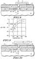
- FIG. 4includes a graph illustrating the relationship of the logarithm of partial pressure of oxygen and temperature to the reduction/oxidation of the copper compounds.
- the y-axis for the graphis the logarithm of oxygen partial pressure (Log pO2) when the pressure is in units of atmospheres.
- the graphhas three curves, two of which are related to copper compounds.
- the reaction conditionsfavor the formation of CuO.
- the reaction conditionsfavor the formation of Cu 2 O.
- the reaction conditionsfavor the formation of Cu.
- the reaction conditionsfavor the formation of Cu.
- the reaction conditionsfavor the formation of Cu.
- the reaction conditionsfavor the formation of Cu.
- the reaction conditionsfavor the formation of Cu.
- the reaction conditionsfavor the formation of Cu.
- the temperatureis about 400 degrees Kelvin and Log p02 is about -60, Cu should be formed.
- the temperatureis about 400 degrees Kelvin and Log p02 is about -60, Cu should be formed.
- the curveindicates that at higher temperatures, a higher oxygen partial pressure is needed to oxidize Cu.
- the lowermost curve in FIG 4is for Re and ReO 2 . This curve is similar to the copper-related curves previously discussed. It is noted that the curve for ReO 2 /ReO 3 is not shown in FIG. 4, but it would lie between the Cu 2 O/Cu curve and the Re/ReO 2 curve.
- FIG. 4shows that Re is more readily oxidized to ReO 2 compared to Cu being oxidized to Cu 2 O or CuO because Re oxidizes at a lower Log p02 compared to Cu for a given temperature.
- Both Re and ReO 2are conductive, and a layer of Re and ReO 2 may be used over the interconnect 145 to lessen the likelihood that the Cu within the interconnect 145 will be oxidized.
- a conductive layer 161is formed over the molybdenum and copper layers 144 and 145 as shown in FIG. 5.
- the conductive layer 161includes Re and ReO 2 , wherein about 5-95 atomic percent of all atomic rhenium in the layer is Re and the balance of the atomic rhenium in the layer is ReO 2 .
- the formation of conductive layer 161may be performed using the deposition and patterning methods previously described for Ru and RuO 2 except that ruthenium is being replaced by rhenium.
- a passivation layer 171is formed over the conductive layer 161 to form a substantially completed integrated circuit as shown in FIG. 6. Other layers and electrical connections (not shown) may be formed if needed.
- FIG. 7includes a cross-sectional view of a portion of a semiconductor device that includes: a semiconductor substrate 10; a metal-oxide-semiconductor transistor 30 having source/drain regions 301, a gate dielectric layer 302, and a gate electrode 303; field isolation regions 31 adjacent to the transistor 30; a first planarized insulating layer 32, a titanium dioxide layer 33, a contact plug 34, and a bottom electrode 35 that is about 50-200 nm (500-2000 angstroms) thick and comprises platinum. Conventional techniques are used to form the semiconductor device up to this point in the process. The titanium dioxide layer 33 and the bottom electrode 35 will contact a subsequently formed ferroelectric layer.
- Layer 33 and 35may be replaced by or used in conjunction with other materials, but those materials must not react with the ferroelectric layer or allow underlying silicon-containing layers to react with the ferroelectric layer. Also, layer 33 must act as an insulator. In other embodiments, layer 33 may include oxides of magnesium, zirconium, tantalum, or the like. Electrode 35 must act as a conductor. In other embodiments, electrode 35 may include palladium, titanium nitride, metals and/or their conductive metal oxides (if the metal can form a conductive metal oxide), or the like.
- a patterned ferroelectric layer 41 about 70-200 nm (700-2000 angstroms) thickis formed over the bottom electrode 35 as shown in FIG. 8.
- the ferroelectric layer 41includes lead zirconate titanate (PZT). It is noted that the word “zirconium” is sometimes used in place of “zirconate,” but this is still the same material.
- the ferroelectric layeris deposited by spin coating, sputter depositing, or metalorganic chemical vapor deposition.
- the ferroelectric layeris annealed in an oxidizing ambient at about atmospheric pressure and a temperature in a range of 550-750 degrees Celsius. The annealing time is about 5-30 minutes if a furnace is used and about 10-300 seconds if a rapid thermal processor is used.
- the oxidizing ambientmay include oxygen by itself or in combination with relatively inert gases, such as nitrogen, argon, helium, and the like.
- relatively inert gasessuch as nitrogen, argon, helium, and the like.
- Non-oxidizing ambientssuch as relatively inert gases without oxygen (nitrogen, argon, helium, or the like) and particularly reducing ambients, such as hydrogen, should be avoided unless the ferroelectric layer is subsequently annealed in an oxidizing ambient.
- a masking layer(not shown) is formed over the ferroelectric layer 41.
- the ferroelectric layer 41is patterned by wet or dry etching techniques. Wet etching may be performed with a solution including hydrofluoric acid, nitric acid, and hydrogen peroxide. The solution is maintained at about room temperature during the etch. Dry etching may be performed using plasma etching or ion milling. For plasma etching, the etching chemistry should include oxygen, fluorine-containing compounds, such as carbon tetrafluoride (CF 4 ) and the like, and chlorine-containing compounds, such as carbon tetrachloride (CCl 4 ), molecular chlorine (Cl 2 ), and the like. After patterning, the masking layer (not shown) is removed to give the patterned ferroelectric layer 41 as shown in FIG. 8.
- FIG. 9is similar to FIG. 4 except that the graph has one curve for elemental lead (Pb) and lead oxide (PbO) and one curve for Ru and RuO 2 .
- the curveindicates that at higher temperatures, a higher oxygen partial pressure is needed to keep PbO from being reduced to Pb.
- FIG. 9shows that RuO 2 is more readily reduced to Ru compared to PbO being reduced to Pb. Both Ru and RuO 2 are conductive, and both do not significantly react with PZT.
- Ru and RuO 2may be used as the top electrode for the ferroelectric capacitor.
- Re and any of its oxides, Ir and IrO 2 , Os and OsO 4may be used as the top electrode.
- the top electrodemust include both the elemental metal and its conductive metal oxide.
- a patterned top electrode 61is formed to cover the top and outer sides of the ferroelectric layer 41.
- the top electrode 61includes Ru and RuO 2 , where about 5-95 percent of all of the atomic ruthenium in the top electrode 61 is RuO 2 and the balance of the atomic ruthenium in the top electrode 61 is Ru. It is noted that the top electrode 61 has more RuO 2 concentration compared to layer 21 or 161 because the top electrode 61 is to protect the PZT in the ferroelectric layer 41.
- Top electrode 61is formed by sputter depositing a layer about 50-500 nm (500-5000 angstroms) thick using any of the methods previously described in forming the top electrode 61. Similar methods are used if the layer includes Re and any of its oxides, Ir and IrO 2 , Os and OsO 4 , or the like.
- a masking layer(not shown) is formed over the layer of Ru and RuO 2 and patterned using a conventional lithographic technique.
- the layer of Ru and RuO 2is patterned by ion milling or by plasma etching the exposed portion of the layer. If the layer includes Ru and RuO 2 , the plasma etching chemistry may include oxygen or fluorine-containing compounds, such as carbon tetrafluoride (CF 4 ) and the like. If other materials are used, other etching chemistries may be used.
- the masking layer(not shown) is removed thereby leaving the top electrode 61 as shown in FIG. 10.
- the top electrode 61protects the top and outer sides of the ferroelectric layer 41.
- the RuO 2 in the top electrode 61may be reduced to form Ru.
- the top electrode 61lessens the likelihood that the ferroelectric layer 41 would be reduced during subsequent processing.
- a reducing agentmust migrate through the top electrode 61 without reducing RuO 2 . In this manner, the ferroelectric layer 41 may be better protected from reduction.
- the other metals and their conductive metal oxidesmay be replaced by or used in conjunction with the layer of Ru and RuO 2 .
- a substantially completed integrated circuitis formed as shown in FIG. 11.
- a second planarized insulation layer 71is formed on the titanium dioxide layer 33 and the top electrode 61.
- An opening in layer 71is formed that extends to the top electrode 61.
- a conductive plugis formed within the opening that includes a titanium nitride layer 72 and a tungsten layer 73.
- Other materialsmay be used in the conductive plug, but the ability of the Ru and RuO 2 to oxidize and reduce may limit the choices.
- the material used for the conductive plugshould remain conductive.
- the layer that contacts the top electrode 61may include titanium tungsten, tungsten, elemental metals and their conductive metal oxides, or the like.
- An interconnect 74 and a passivation layer 75are formed over the conductive plug and layer 71. Other interlevel insulating and interconnecting layers may be formed, if needed. Electrical connections to other parts of the integrated circuit, such as the gate electrode 303 and the left-hand source/drain region 301, are formed but are not shown in FIG 11.
- the present inventionmay be used to form a protective layer.
- the protective layermay be used for any number of devices.
- Silicon nitrideis a good hydrogen barrier, but silicon nitride cannot come in direct contact with a PZT layer because of possible reactions between silicon and the PZT materials.
- hydrogenmay be produced during the formation of the silicon nitride layer, depending on the deposition chemistry chosen, that may reduce the oxide compounds within the ferroelectric layer.
- This applicationshows how a ferroelectric layer may be virtually encapsulated by protective layers including silicon nitride.
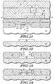
- FIG. 12includes a cross-sectional view of a portion of semiconductor device that includes a first insulating layer 80 and a bottom electrode 81 that includes elemental iridium (Ir) or a mixture of Ir and iridium dioxide (IrO 2 ).
- the bottom electrode 81is deposited and patterned similar to the other layers previously described that include metals and their conductive metal oxides.
- a patterned second insulating layer 91is formed over the first insulating layer 80 and part of the bottom electrode 81.
- a silicon nitride layeris deposited and anisotropically etched to form nitride sidewall spacers 92 as shown in FIG. 13.
- a layer of titanium dioxideis also deposited and anisotropically etched to form titanium dioxide spacers 93 as shown in FIG. 13.
- the titanium dioxide layermay be replaced or used in conjunction with oxides of magnesium, zirconium, tantalum; or the like.
- the titanium dioxide layerdoes not need to be anisotropically etched, but covers all of the exposed surfaces of the semiconductor device. This optional embodiment is not shown in FIG. 13.
- hydrogenmay have been generated and reduced IrO 2 , if any was originally present.
- a short anneal using an oxidizing ambientmay be performed, if needed, to oxidize some of the Ir to IrO 2 .
- IrO 2should make up between 5-95 atomic percent of all of the iridium within the bottom electrode 81.
- a ferroelectric layer 101is formed that includes lanthanum-doped PZT as seen in FIG. 14.
- the ferroelectric layer 101is deposited by one of the methods previously discussed in conjunction with layers that include PZT.
- the substrate including the ferroelectric layer 101is patterned by chemical-mechanical polishing. To ensure that all of the ferroelectric layer 101 over the insulating layer 91 is removed, the ferroelectric layer 101 is wet etched using a solution including hydrofluoric acid, nitric acid, and hydrogen peroxide. In addition to removing any residual ferroelectric layer 101, the wet etching step also etches some of the ferroelectric layer 101 within the opening to make certain that the ferroelectric layer 101 only contacts the titanium dioxide spacers 93 and the bottom electrode 81.
- the substrate including the ferroelectric layer 101is annealed in a manner similar to the ferroelectric layer 41 that was previously described.
- a top electrode 111is formed and includes elemental osmium (Os) and osmium tetraoxide (OsO 4 ) as seen in FIG. 15.
- the OsO 4makes up about 5-95 atomic percent of the total osmium in the top electrode 111, and the balance of the osmium in the top electrode 111 is Os.
- the top electrode 111is deposited and patterned similar to the other layers previous described that include metals and their conductive metal oxides. Other layers and electrical connections are made to the ferroelectric capacitor, but are not shown in the figures.
- the ferroelectric layerhas electrodes 81 and 111 that include metals and their conductive metal oxides.
- Nitride spacers 92surround the sides of the ferroelectric layer 101 but do not contact the ferroelectric layer 101. Hydrogen should not contact the ferroelectric layer 101 via the sides because the nitride spacers 92 should act as a hydrogen barrier.
- the ferroelectric layer 101was not reduced by hydrogen that is produced during the nitride spacer formation because the nitride spacers 92 were formed prior to the ferroelectric layer 101.
- the titanium dioxide spacers 93separate the nitride spacers 92 and the ferroelectric layer 101.
- the silicon within the nitride spacers 92should not react with the ferroelectric layer 101.
- the electrodes 81 and 111 and the silicon nitride spacers 92virtually encapsulate the ferroelectric layer 101. With this embodiment, reduction of the ferroelectric layer 101 is less likely than with conventional ferroelectric capacitors.
- FIG. 16includes another embodiment having a protected ferroelectric layer.
- FIG. 16has an oxide layer 80 and a first silicon nitride layer 81.
- a conductive layer 121which includes Re and ReO 2
- a ferroelectric layer 122which includes PZT, are formed over the first silicon nitride layer 81.
- the conductive layer 121acts as the bottom electrode, and ReO 2 within the conductive layer 121 lessens the likelihood of reducing the ferroelectric layer 122.
- the layers 121 and 122are patterned using ion milling. The ion milling patterns the layers 121 and 122 so that they are coincident with each other.
- a titanium dioxide layer 123 and a second silicon nitride layer 124are formed over the insulating layer 80 including the layers 121 and 122.
- the layers 123 and 124are anisotropically etched to form sidewall spacers. The etch to form sidewall spacers may be performed in one or more steps.
- the deposition of silicon nitridegenerates hydrogen that may reduce the PbO within the ferroelectric layer.
- the substrate including the ferroelectric layer 122is annealed in an oxidizing ambient. This anneal is similar to the anneal used for ferroelectric layer 41 that was previously described.
- a top electrode 125 including Ru and RuO 2is formed over the ferroelectric layer 122 and the sidewall spacers.
- RuO 2 within the top electrode 125lessens the likelihood of reducing the ferroelectric layer 122.
- Both the conductive layer 121, which acts as the bottom electrode, and the ferroelectric layer 122are virtually encapsulated by the first silicon nitride layer 81, the second silicon nitride layer 124 of the sidewall spacers, and the top electrode 125. Because it is not completely known if the degradation problems with ferroelectric capacitors are related to the bottom electrode or the ferroelectric layer, this embodiment may be effective against degradation problems since the bottom electrode and ferroelectric layer are more encapsulated than in other embodiments.
- FIG. 17includes a cross-sectional view of a portion of a semiconductor device having a ferroelectric capacitor and shielding layers to protect the ferroelectric capacitors from reducing agents.
- the substrateincludes a first insulating layer 130 and a titanium dioxide layer 131.
- a polysilicon plug 132is covered by a first conductive layer 133, made of eg. Ru and RuO 2 , that defines the first electrode of the capacitor.
- a ferroelectric layer 134lies over the first conductive layer 133, and a layer 135 including platinum lies over the ferroelectric layer 134.
- the layer 135acts as the second electrode for the capacitor.
- the formation of the device up to this point in the process, including the anneal of the ferroelectric layer 134are conventional.
- a second insulating layer 136is formed over the electrode and is thick enough so that there is little, if any, capacitive coupling between the layer 135 and subsequently formed shielding layer.
- the second insulation layer 136is at least about 500 nm (5000 angstroms) thick.
- the substrate including the second insulating layer 136is annealed in an oxidizing ambient to lessen the amount of hydrogen that may be trapped within the second insulating layer 136.
- Shielding layers 137 and 138are formed over the second insulating layer 136.
- Shielding layer 137includes a mixture of Ru and RuO 2 similar to layer 61.
- Shielding layer 138includes silicon nitride and is formed by sputter deposition or plasma-enhanced chemical vapor deposition. The temperature and amount of hydrogen present during the silicon nitride deposition should be relatively low to minimize the reduction of RuO 2 to Ru within layer 137.
- the substrateis annealed in an oxidizing ambient to help oxidize some of the Ru within layer 137 and to seal any pinholes that may be present within layer 138.
- the reducing agentFor a reducing agent, such as hydrogen, to interfere with the ferroelectric capacitor, the reducing agent must not only pass through layer 138 but also pass through layer 137 without reducing the RuO 2 to Ru within layer 137.
- This embodimentnot only illustrates a good hydrogen barrier, but also shows that the shielding layers do not have to electrically participate in the semiconductor device if this is so desired.
Landscapes
- Engineering & Computer Science (AREA)
- Physics & Mathematics (AREA)
- Condensed Matter Physics & Semiconductors (AREA)
- General Physics & Mathematics (AREA)
- Computer Hardware Design (AREA)
- Microelectronics & Electronic Packaging (AREA)
- Power Engineering (AREA)
- Manufacturing & Machinery (AREA)
- Semiconductor Memories (AREA)
- Fixed Capacitors And Capacitor Manufacturing Machines (AREA)
- Semiconductor Integrated Circuits (AREA)
Description
- The present invention relates to the field of semiconductordevices, and in particular, to a process for forming a semiconductor device having alayer including an elemental metal and its conductive metal oxide.
- Semiconductor devices may have a layer in which electricalcharacteristics are changed if the layer is oxidized or reduced.With conductive materials, such as substrate regions, siliconmembers, contacts, vias, and interconnects and the like, oxidationis typically to be prevented or at least minimized. Conventionalmaterials used for conductive materials may include silicon(monocrystalline, polycrystalline, and amorphous), metals, andmetal-containing compounds. Oxides of most of these materialstypically are insulators. The formation of insulating oxides canresult in electrical opens, which may not be desired.
- In some semiconductor devices, reducing agents may pose aproblem. In capacitors using oxide ferroelectric materials as thedielectric, a reducing atmosphere may cause the ferroelectric tobecome degraded. The ferroelectric may lose enough of itsferroelectric properties to become virtually useless as aferroelectric capacitor. Ferroelectric capacitors appear to bemore sensitive with respect to this problem than manysemiconductor devices. Processing with a relatively inertambient, such as nitrogen, argon, helium, and the like, without anyoxidizing gases may still cause ferroelectric capacitors tobecome degraded.
- In addition to ferroelectric capacitors, other semiconductordevices may have problems with reducing agents, such ashydrogen. Hydrogen may accelerate hot electron degradation ofmany types of electrically programmable read only memories(EPROMs) and particularly electrically erasable EPROMs(EEPROMs). Hot carrier transport through a gate or tunnel dielectric layer generally lessens the number of times the EEPROMmay be cycled, wherein a cycle is the combination of a programmingstep and an erasing step. Also, hydrogen may react with oxygen toform moisture. Moisture in an EPROM generally causes data retentionproblems.
EP 0 478 799 is related to a semiconductor device with aferroelectric capacitor. After forming a transistor, a contact andlower electrode for the ferroelectric capacitor are formed. After acontact opening is formed to a source region of the transistor, aconductive metal oxide is formed within the contact followed by aplatinum layer.The conductive metal oxide protects the underlying source regionfrom oxidation. A lead-containing ferroelectric layer is formed overthe platinum layer. After patterning the conductive metal oxide,platinum, and ferroelectric layers, an insulating layer is formed andpatterned to define contact openings to the drain region and theferroelectric layer. An aluminum layer is deposited and patterned toform contacts and the upper plate of the ferroelectric capacitor.- Although the conductive metal oxide is present within thedevice during the formation of the insulating layer, the ferroelectriclayer is exposed during the insulating layer formation. Manyinsulating layers are formed with an ambient that includes hydrogenwithin a silicon source (silane or tetraethylorthosilicate). Thehydrogen may reduce the ferroelectric layer after the ferroelectriclayer was oxidized. Therefore, there is a significant risk ofconverting the ferroelectric layer from its perovskite state.
- U.S. 4,851,895 is related to the use of ruthenium as aninterconnect metalization. Some of the ruthenium can be converted toruthenium dioxide during subsequent processing.
- The present invention provides a process for forming a semiconductordevice as set out in the accompanying claims.
- Other features and advantages of the present invention will be apparentfrom the accompanying drawings and from the detailed description that follows.
- The present invention is illustrated by way of example andnot limitation in the figures of the accompanying drawings, inwhich like references indicate similar elements, and in which:
- FIGs. 1 and 2 each include a cross-sectional view of aportion of a substrate at various process steps in forming a layerhaving a metallic compound that includes an elemental metal andits conductive metal oxide over a contact plug.
- FIGs. 3, 5, and 6 each include a cross-sectional view of aportion of a substrate at various process steps in forming a layerhaving a metallic compound that includes an elemental metal andits conductive metal oxide over an interconnect.
- FIGs. 4 and 9 each include a graph showing various materialsand their oxidation states given the logarithm of partial pressureof oxygen at the material and the temperature of the material.
- FIGs. 7, 8, 10, and 11 each include a cross-sectional viewof a portion of a substrate at various process steps in forming anelectrode for a ferroelectric capacitor, wherein the electrodeincludes an elemental metal and its conductive metal oxide inaccordance with an embodiment of the present invention.
- FIGs. 12-17 each include a cross-sectional view of aportion of a substrate illustrating a layer that includes anelemental metal and its conductive metal oxide in accordancewith another embodiment of the present invention.
- The present invention includes a process for forming a semiconductor devicehaving a material including an elemental, metal and its conductivemetal oxide, wherein the conductive metal oxide is capable of beingreduced preferentially to an adjacent dielectric region of the device. Thematerial lessens the likelihood that the adjacent region isreduced when this is undesired. A general descriptionis followed by applications in which the material may be used.The applications that are described below are illustrative and arenot meant to be limiting.
- Gibbs free energy changes are used to determine whichmaterial should be placed adjacent to a region to lessen thelikelihood of oxidizing or reducing the region. For example, if theadjacent region is not to be reduced, the material should be moreeasily reduced compared to the adjacent region, and if theadjacent region is not to be oxidized, the material should be moreeasily oxidized compared to the adjacent region. Many materialscannot be used within a semiconductor device because a change in oxidationstate changes the electrical properties of the material. Forexample, titanium is a conductor and can be oxidized to form atitanium oxide (TiOx where x is no more than two.) Titaniummonoxide (TiO) is a semiconductor, and titanium dioxide (TiO2) isan insulator. Therefore, the titanium material may change from aconductor to a semiconductor or an insulator or vice versa. Thesechanges usually cause unwanted electrical characteristics withina semiconductor device. In order to avoid the transformationfrom a conductor to a semiconductor or an insulator or vice versa,the material in both its oxidized and reduced forms should eitherbe both conductors, both semiconductors, or both insulators.
- A category of materials that may be usedare metals that can form conductive metal oxides.Ruthenium (Ru), rhenium (Re), iridium (Ir), and osmium (Os) areconductive and can be oxidized to form ruthenium dioxide (RuO2),rhenium dioxide (ReO2) or rhenium trioxide (ReO3), iridium dioxide (IrO2), and osmium tetraoxide (OsO4), respectively, whichare also conductive. Below illustrates the reaction for ruthenium:
- The present invention requires a mixture of the metal andits conductive metal oxide. The mixture allows the reactions tobe more freely reversible compared to having just the metal orjust the conductive metal oxide. If both are not present, extraenergy and more importantly longer times are needed to form amixture. Since the mixture is to be preferentially reduced, themixture should have enough of the conductive metal oxide, such asRuO2, to lessen the likelihood of reducing an adjacent region.The present invention may be used ina variety of applications includingferroelectric capacitors.As used hereinafter, "elemental metal" is amonoatomic metallic material, such as Ru, Re, Ir, Os.Some elemental metals have conductive metal oxides,such as RuO2, ReO2, ReO3, IrO2, OsO4.
- An example not part of the present invention relates to acontact or via plug within a semiconductor device. The plug maybe used to lessen the likelihood that an underlying layer would beoxidized or reduced. FIG. 1 includes a cross-sectional view of aportion of a semiconductor device having a
substrate 10, a dopedregion 11 within thesubstrate 10, apatterned oxide layer 12, andasilicon plug 13. If the substrate would be oxidized, part of thesilicon plug 13 would form to a silicon dioxide layer. Before aninterconnect is formed over theplug 13, the silicon dioxide layer would have to be removed. The removal of the silicon dioxidelayer may also remove the part of the patternedoxide layer 12.Therefore, it is advantageous to protect thesilicon plug 13 priorto an oxidation step. - A
conductive layer 21 is formed over theoxide layer 12 andpatterned to form a protective cap over thesilicon plug 13 asshown in FIG. 2. Theconductive layer 21 includes a mixture of anelemental metal and its conductive metal oxide.Layer 21 may beformed by sputter depositing using a target having a mixture ofthe elemental metal and the conductive metal oxide. When thelayer includes Ru and RuO2, about 5-95 percent of all of theatomic ruthenium in the sputter target is Ru and the balance ofthe atomic ruthenium in the target is RuO2. In this case, thesputter target andlayer 21 have similar compositions.Layer 21may be formed using other methods. For example, reactive ionsputtering using a Ru target and a plasma including oxygen may beused to depositlayer 21. In addition, a layer of Ru may be formedby sputter deposition or chemical vapor deposition andsubsequently oxidized to convert only part of the Ru to RuO2. Inanother embodiment, a layer of Ru and a layer of RuO2 may besequentially deposited. Additional layers of Ru and RuO2 may bedeposited. Regardless of the method used to formlayer 21, about5-95 percent of all atomic ruthenium present inlayer 21 is Ruand balance of the atomic ruthenium in thelayer 21 is RuO2. Inother embodiments,layer 21 may include Re and any of its oxides,Ir and IrO2, Os and OsO4, or the like. As used in thisspecification, "Re and any of its oxides" includes Re and ReO2, Reand ReO3, or Re and ReO2 and ReO3. - A masking layer (not shown) is formed over the
layer 21 andpatterned using a conventional lithographic technique. Thelayer 21 is patterned by ion milling the exposed portions of thelayer 21 or by plasma etching the exposed portions oflayer 21. If thelayer 21 includes Ru and RuO2, the plasma etching chemistry mayinclude oxygen or fluorine-containing compounds, such as carbontetrafluoride (CF4) and the like. If other materials are used,other etching chemistries may be used. After the patterning step,the masking layer (not shown) is removed. - As can be seen in FIG. 2, the
layer 21 covers thesilicon plug 13. Thelayer 21 lessens the likelihood that thesilicon plug 13would be oxidized during a subsequent oxidation step. The Ru inlayer 21 may be oxidized to form RuO2. In order forsilicon plug 13 to be oxidized under thelayer 21, oxygen must migrate throughthelayer 21 before it reacts with the Ru inlayer 21. Also, thelayer 21 stays conductive even if the Ru is oxidized. A titaniumlayer cannot be used in place oflayer 21 because titanium, whichis a conductor, oxidizes to become titanium dioxide, which is aninsulator. In other examples, theplug 13 may include a metaland its conductive metal oxide instead of silicon. In this manner,thesubstrate 10 and theregion 11 may be better protected fromoxidation, and electrical connections throughplug 13 may bemaintained. - Both contact and via plugs may be formed using the presentteaching. For example, plug 13 shown in FIG. 1 may compriseRu and RuO2 that may lessen the likelihood of oxidizing a regionwithin the substrate adjacent to the
plug 13. Similarly, plug 13may contact a silicon member, such as a gate electrode to preventits oxidation. Ifplug 13 includes Ru and RuO2,layer 21 shown inFIG. 2 is not needed. If hydrogen migration into regions within thesubstrate is a concern, about 5-95 atomic percent of allruthenium within theplug 13 should be RuO2. - An example not part of the present invention and relatingto interconnects issimilar to that for contact or via plugs: FIG. 3 includes a cross-sectionalview of a portion of an integrated circuit including: a
semiconductor substrate 10, a dopedregion 11 within thesubstrate 10, a first insulatinglayer 12 with a contact opening, acontact plug within the contact opening that includes atitaniumnitride layer 141 and atungsten layer 142. A second insulatinglayer 143 overlies the first insulatinglayer 12 and the contactplug. The secondinsulating layer 143 includes an interconnectingchannel. Amolybdenum layer 144 and acopper layer 145 aredeposited over the second insulatinglayer 143 and within theinterconnecting channel. The substrate is chemically-mechanicallypolished to remove portions of the molybdenum andcopper layers - A problem with copper is that it may be oxidized. Belowillustrates the reactions for forming various copper compounds:
- FIG. 4 includes a graph illustrating the relationship of thelogarithm of partial pressure of oxygen and temperature to thereduction/oxidation of the copper compounds. The y-axis for thegraph is the logarithm of oxygen partial pressure (Log pO2) whenthe pressure is in units of atmospheres. The graph has threecurves, two of which are related to copper compounds. In theupper, left-hand part of the uppermost curve, the reactionconditions favor the formation of CuO. In the region between theuppermost and intermediate curve, the reaction conditions favorthe formation of Cu2O. In the lower, right-hand side of theintermediate curve, the reaction conditions favor the formationof Cu. For a given temperature and oxygen partial pressure, onecan predict which product (Cu, Cu2O, or CuO) should be formed.For example, if the temperature is about 400 degrees Kelvin andLog p02 is about -60, Cu should be formed. Similarly, at about400 degrees Kelvin and Log p02 of about -20, CuO should beformed. The curve indicates that at higher temperatures, a higheroxygen partial pressure is needed to oxidize Cu.
- The inventors believe that placing a material that is morereadily oxidized than Cu lessens the likelihood that Cu is oxidizedto Cu2O or CuO. The lowermost curve in FIG 4 is for Re and ReO2.This curve is similar to the copper-related curves previouslydiscussed. It is noted that the curve for ReO2/ReO3 is not shownin FIG. 4, but it would lie between the Cu2O/Cu curve and theRe/ReO2 curve. FIG. 4 shows that Re is more readily oxidized toReO2 compared to Cu being oxidized to Cu2O or CuO because Reoxidizes at a lower Log p02 compared to Cu for a giventemperature. Both Re and ReO2 are conductive, and a layer of Reand ReO2 may be used over the
interconnect 145 to lessen the likelihood that the Cu within theinterconnect 145 will beoxidized. - A
conductive layer 161 is formed over the molybdenum andcopper layers conductivelayer 161 includes Re and ReO2, wherein about 5-95 atomicpercent of all atomic rhenium in the layer is Re and the balance ofthe atomic rhenium in the layer is ReO2. The formation ofconductive layer 161 may be performed using the deposition andpatterning methods previously described for Ru and RuO2 exceptthat ruthenium is being replaced by rhenium. Apassivation layer 171 is formed over theconductive layer 161 to form asubstantially completed integrated circuit as shown in FIG. 6.Other layers and electrical connections (not shown) may beformed if needed. - The present invention may be used in forming ferroelectriccapacitors. FIG. 7 includes a cross-sectional view of a portion ofa semiconductor device that includes: a
semiconductor substrate 10; a metal-oxide-semiconductor transistor 30 havingsource/drain regions 301, agate dielectric layer 302, and agateelectrode 303;field isolation regions 31 adjacent to thetransistor 30; a first planarized insulatinglayer 32, atitaniumdioxide layer 33, acontact plug 34, and abottom electrode 35that is about 50-200 nm (500-2000 angstroms) thick and comprises platinum.Conventional techniques are used to form the semiconductordevice up to this point in the process. Thetitanium dioxide layer 33 and thebottom electrode 35 will contact a subsequentlyformed ferroelectric layer.Layer layer 33 must act as an insulator. In other embodiments,layer 33 may include oxides of magnesium, zirconium, tantalum,or the like.Electrode 35 must act as a conductor. In otherembodiments,electrode 35 may include palladium, titaniumnitride, metals and/or their conductive metal oxides (if the metalcan form a conductive metal oxide), or the like. - A patterned
ferroelectric layer 41 about 70-200 nm (700-2000angstroms) thick is formed over thebottom electrode 35 as shownin FIG. 8. Theferroelectric layer 41 includes lead zirconatetitanate (PZT). It is noted that the word "zirconium" issometimes used in place of "zirconate," but this is still the samematerial. The ferroelectric layer is deposited by spin coating,sputter depositing, or metalorganic chemical vapor deposition.The ferroelectric layer is annealed in an oxidizing ambient atabout atmospheric pressure and a temperature in a range of 550-750degrees Celsius. The annealing time is about 5-30 minutes ifa furnace is used and about 10-300 seconds if a rapid thermalprocessor is used. The oxidizing ambient may include oxygen byitself or in combination with relatively inert gases, such asnitrogen, argon, helium, and the like. Non-oxidizing ambients,such as relatively inert gases without oxygen (nitrogen, argon,helium, or the like) and particularly reducing ambients, such ashydrogen, should be avoided unless the ferroelectric layer issubsequently annealed in an oxidizing ambient. - A masking layer (not shown) is formed over the
ferroelectric layer 41. Theferroelectric layer 41 is patterned bywet or dry etching techniques. Wet etching may be performedwith a solution including hydrofluoric acid, nitric acid, andhydrogen peroxide. The solution is maintained at about roomtemperature during the etch. Dry etching may be performed usingplasma etching or ion milling. For plasma etching, the etchingchemistry should include oxygen, fluorine-containing compounds,such as carbon tetrafluoride (CF4) and the like, and chlorine-containingcompounds, such as carbon tetrachloride (CCl4),molecular chlorine (Cl2), and the like. After patterning, the masking layer (not shown) is removed to give the patternedferroelectric layer 41 as shown in FIG. 8. - As previously discussed, one problem with ferroelectriccapacitors is their inability to retain their ferroelectricproperties. Although the source of the problem is not known, it ispossible that the ferroelectric layer is being at least partiallyreduced during subsequent processing. Of the materials in PZT,lead is the most readily reduced. FIG. 9 is similar to FIG. 4 exceptthat the graph has one curve for elemental lead (Pb) and leadoxide (PbO) and one curve for Ru and RuO2. The curve indicatesthat at higher temperatures, a higher oxygen partial pressure isneeded to keep PbO from being reduced to Pb. FIG. 9 shows thatRuO2 is more readily reduced to Ru compared to PbO being reducedto Pb. Both Ru and RuO2 are conductive, and both do notsignificantly react with PZT. Therefore, Ru and RuO2 may be usedas the top electrode for the ferroelectric capacitor. Similarly, Reand any of its oxides, Ir and IrO2, Os and OsO4 may beused as the top electrode. The top electrode must include boththe elemental metal and its conductive metal oxide.
- Referring to FIG. 10, a patterned
top electrode 61 is formedto cover the top and outer sides of theferroelectric layer 41. Thetop electrode 61 includes Ru and RuO2, where about 5-95 percentof all of the atomic ruthenium in thetop electrode 61 is RuO2 andthe balance of the atomic ruthenium in thetop electrode 61 is Ru.It is noted that thetop electrode 61 has more RuO2 concentrationcompared tolayer top electrode 61 is toprotect the PZT in theferroelectric layer 41.Top electrode 61 isformed by sputter depositing a layer about 50-500 nm (500-5000 angstroms)thick using any of the methods previously described in formingthetop electrode 61. Similar methods are used if the layerincludes Re and any of its oxides, Ir and IrO2, Os and OsO4, or thelike. - A masking layer (not shown) is formed over the layer of Ruand RuO2 and patterned using a conventional lithographictechnique. The layer of Ru and RuO2 is patterned by ion milling orby plasma etching the exposed portion of the layer. If the layerincludes Ru and RuO2, the plasma etching chemistry may include oxygen or fluorine-containing compounds, such as carbontetrafluoride (CF4) and the like. If other materials are used,other etching chemistries may be used. After the patterning step,the masking layer (not shown) is removed thereby leaving the
topelectrode 61 as shown in FIG. 10. - As can be seen in FIG. 10, the
top electrode 61 protects thetop and outer sides of theferroelectric layer 41. The RuO2 in thetop electrode 61 may be reduced to form Ru. Thetop electrode 61lessens the likelihood that theferroelectric layer 41 would bereduced during subsequent processing. In order forferroelectriclayer 41 to be reduced, a reducing agent must migrate through thetop electrode 61 without reducing RuO2. In this manner, theferroelectric layer 41 may be better protected from reduction.The other metals and their conductive metal oxides may bereplaced by or used in conjunction with the layer of Ru and RuO2. - A substantially completed integrated circuit is formed asshown in FIG. 11. A second
planarized insulation layer 71 isformed on thetitanium dioxide layer 33 and thetop electrode 61.An opening inlayer 71 is formed that extends to thetop electrode 61. A conductive plug is formed within the opening that includesatitanium nitride layer 72 and atungsten layer 73. Othermaterials may be used in the conductive plug, but the ability ofthe Ru and RuO2 to oxidize and reduce may limit the choices. Thematerial used for the conductive plug should remain conductive.Besides titanium nitride, the layer that contacts thetopelectrode 61 may include titanium tungsten, tungsten, elementalmetals and their conductive metal oxides, or the like. Aninterconnect 74 and apassivation layer 75 are formed over theconductive plug andlayer 71. Other interlevel insulating andinterconnecting layers may be formed, if needed. Electricalconnections to other parts of the integrated circuit, such as thegate electrode 303 and the left-hand source/drain region 301, areformed but are not shown in FIG 11. - The present invention may be used to form a protectivelayer. Although this embodiment is described in conjunction witha ferroelectric layer, the protective layer may be used for anynumber of devices. Silicon nitride is a good hydrogen barrier, butsilicon nitride cannot come in direct contact with a PZT layerbecause of possible reactions between silicon and the PZTmaterials. Also, hydrogen may be produced during the formationof the silicon nitride layer, depending on the deposition chemistrychosen, that may reduce the oxide compounds within theferroelectric layer. This application shows how a ferroelectriclayer may be virtually encapsulated by protective layers includingsilicon nitride. FIG. 12 includes a cross-sectional view of aportion of semiconductor device that includes a first insulating
layer 80 and abottom electrode 81 that includes elementaliridium (Ir) or a mixture of Ir and iridium dioxide (IrO2). Thebottom electrode 81 is deposited and patterned similar to theother layers previously described that include metals and theirconductive metal oxides. A patterned second insulatinglayer 91is formed over the first insulatinglayer 80 and part of thebottom electrode 81. A silicon nitride layer is deposited andanisotropically etched to formnitride sidewall spacers 92 asshown in FIG. 13. A layer of titanium dioxide is also depositedand anisotropically etched to formtitanium dioxide spacers 93 asshown in FIG. 13. In another embodiment, the titanium dioxidelayer may be replaced or used in conjunction with oxides ofmagnesium, zirconium, tantalum; or the like. Optionally, thetitanium dioxide layer does not need to be anisotropically etched,but covers all of the exposed surfaces of the semiconductordevice. This optional embodiment is not shown in FIG. 13. Duringthe formation of the spacers, hydrogen may have been generatedand reduced IrO2, if any was originally present. A short annealusing an oxidizing ambient may be performed, if needed, tooxidize some of the Ir to IrO2. After spacer formation, IrO2should make up between 5-95 atomic percent of all of the iridiumwithin thebottom electrode 81. - A
ferroelectric layer 101 is formed that includeslanthanum-doped PZT as seen in FIG. 14. Theferroelectric layer 101 is deposited by one of the methods previously discussed inconjunction with layers that include PZT. The substrate includingtheferroelectric layer 101 is patterned by chemical-mechanicalpolishing. To ensure that all of theferroelectric layer 101 overthe insulatinglayer 91 is removed, theferroelectric layer 101 iswet etched using a solution including hydrofluoric acid, nitricacid, and hydrogen peroxide. In addition to removing any residualferroelectric layer 101, the wet etching step also etches some oftheferroelectric layer 101 within the opening to make certainthat theferroelectric layer 101 only contacts thetitaniumdioxide spacers 93 and thebottom electrode 81. The substrateincluding theferroelectric layer 101 is annealed in a mannersimilar to theferroelectric layer 41 that was previouslydescribed. - A
top electrode 111 is formed and includes elementalosmium (Os) and osmium tetraoxide (OsO4) as seen in FIG. 15. TheOsO4 makes up about 5-95 atomic percent of the total osmium inthetop electrode 111, and the balance of the osmium in thetopelectrode 111 is Os. Thetop electrode 111 is deposited andpatterned similar to the other layers previous described thatinclude metals and their conductive metal oxides. Other layersand electrical connections are made to the ferroelectriccapacitor, but are not shown in the figures. - In this embodiment, the ferroelectric layer has
electrodes Nitride spacers 92 surround the sides of theferroelectric layer 101 but do not contact theferroelectric layer 101. Hydrogenshould not contact theferroelectric layer 101 via the sidesbecause thenitride spacers 92 should act as a hydrogen barrier.Theferroelectric layer 101 was not reduced by hydrogen that isproduced during the nitride spacer formation because thenitridespacers 92 were formed prior to theferroelectric layer 101. Thetitanium dioxide spacers 93 separate thenitride spacers 92 andtheferroelectric layer 101. Therefore, the silicon within thenitride spacers 92 should not react with theferroelectric layer 101. Theelectrodes silicon nitride spacers 92virtually encapsulate theferroelectric layer 101. With thisembodiment, reduction of theferroelectric layer 101 is lesslikely than with conventional ferroelectric capacitors. - FIG. 16 includes another embodiment having a protectedferroelectric layer. FIG. 16 has an
oxide layer 80 and a firstsilicon nitride layer 81. Aconductive layer 121, which includesRe and ReO2, and a ferroelectric layer 122, which includes PZT,are formed over the firstsilicon nitride layer 81. Theconductivelayer 121 acts as the bottom electrode, and ReO2 within theconductive layer 121 lessens the likelihood of reducing theferroelectric layer 122. Thelayers 121 and 122 are patternedusing ion milling. The ion milling patterns thelayers 121 and 122so that they are coincident with each other. Atitanium dioxidelayer 123 and a secondsilicon nitride layer 124 are formed overthe insulatinglayer 80 including thelayers 121 and 122. Thelayers ferroelectric layer 41 that was previously described. Atop electrode 125 includingRu and RuO2 is formed over the ferroelectric layer 122 and thesidewall spacers. RuO2 within thetop electrode 125 lessens thelikelihood of reducing the ferroelectric layer 122. Both theconductive layer 121, which acts as the bottom electrode, and theferroelectric layer 122 are virtually encapsulated by the firstsilicon nitride layer 81, the secondsilicon nitride layer 124 ofthe sidewall spacers, and thetop electrode 125. Because it is notcompletely known if the degradation problems with ferroelectriccapacitors are related to the bottom electrode or theferroelectric layer, this embodiment may be effective againstdegradation problems since the bottom electrode andferroelectric layer are more encapsulated than in otherembodiments. - FIG. 17 includes a cross-sectional view of a portion of asemiconductor device having a ferroelectric capacitor andshielding layers to protect the ferroelectric capacitors fromreducing agents. The substrate includes a first insulating
layer 130 and atitanium dioxide layer 131. Apolysilicon plug 132 iscovered by a firstconductive layer 133, made of eg. Ru and RuO2, thatdefines the first electrode of the capacitor. Aferroelectric layer 134 lies over the firstconductive layer 133, and alayer 135 including platinum lies over theferroelectric layer 134. Thelayer 135acts as the second electrode for the capacitor. The formation ofthe device up to this point in the process, including the anneal oftheferroelectric layer 134, are conventional. A second insulatinglayer 136 is formed over the electrode and is thick enough so thatthere is little, if any, capacitive coupling between thelayer 135 and subsequently formed shielding layer. Typically, thesecond insulation layer 136 is at least about 500 nm (5000 angstroms)thick. The substrate including the second insulatinglayer 136 isannealed in an oxidizing ambient to lessen the amount of hydrogenthat may be trapped within the second insulatinglayer 136. - Shielding layers 137 and 138 are formed over the secondinsulating
layer 136.Shielding layer 137 includes a mixture ofRu and RuO2 similar tolayer 61.Shielding layer 138 includessilicon nitride and is formed by sputter deposition or plasma-enhancedchemical vapor deposition. The temperature and amountof hydrogen present during the silicon nitride deposition should berelatively low to minimize the reduction of RuO2 to Ru withinlayer 137. After deposition oflayer 138, the substrate isannealed in an oxidizing ambient to help oxidize some of the Ruwithinlayer 137 and to seal any pinholes that may be presentwithinlayer 138. For a reducing agent, such as hydrogen, tointerfere with the ferroelectric capacitor, the reducing agentmust not only pass throughlayer 138 but also pass throughlayer 137 without reducing the RuO2 to Ru withinlayer 137. Thisembodiment not only illustrates a good hydrogen barrier, but alsoshows that the shielding layers do not have to electricallyparticipate in the semiconductor device if this is so desired.
Claims (10)
- A process for forming a semiconductor device comprising the steps of:wherein the conductive metal oxide is capable of being reduced to theelemental metal preferentially to the first region being reduced.providing a substrate (10; 80, 81; 130, 131) having a primary surface;forming a first region (41; 101; 122; 134) at a locationoverlying the substrate, and wherein the first region is adielectric region;depositing a first layer (61; 111; 125; 137) over the first region,wherein the step of depositing the first layer issuch that:the first layer as deposited, has a mixture which includes an elementalmetal and its conductive metal oxide;
- The process of claim 1, wherein theelemental metal and its conductive metal oxide are one of the followingpairs: ruthenium and ruthenium dioxide; rhenium and any of its oxides;iridium and iridium dioxide; or osmium and osmium tetraoxide.
- The process of any preceding claim, wherein
the first layer has a plurality of first atoms;
the conductive metal oxide has a plurality of the first atoms; and
at least 5 atomic percent of the first atoms within the first layer is in theconductive metal oxide. - The process of any preceding claim wherein the semiconductor deviceincludes a ferroelectric capacitor that includes a first electrode (35; 81;121; 133), a ferroelectric layer (41; 101; 122; 134) overlying the firstelectrode; and a second electrode (61; 111; 125; 135) overlying theferroelectric layer, wherein the ferroelectric layer (41; 101; 122; 134) is thefirst region.
- The process of claim 4 further comprising the step of:forming the first electrode before forming the ferroelectric layer, whereinpatterning the first layer forms the second electrode.
- The process of claim 4 or 5, wherein the ferroelectric capacitor is furthersuch that:the ferroelectric layer (41; 101; 122) includes lead;the element metal is ruthenium and its conductive metal oxide is rutheniumdioxide;the first layer (61; 111; 125) has a plurality of ruthenium atoms; andat least 5 atomic percent of the ruthenium atoms within the first layer (61;111; 125) are in the ruthenium dioxide.
- The process of any one of claims 1 to 3, wherein the semiconductordevice includes a ferroelectric capacitor that includes a first electrode(133), a ferroelectric layer (134) overlying the first electrode (133) and asecond electrode (135), overlying the ferroelectric layer (134), wherein theferroelectric layer (134) is the first region, and the process furthercomprises the steps of:wherein the process is furthercharacterized by depositing the first layer(137) such that:forming the first electrode (133); andforming the second electrode (135),the first layer (137) overlies and is spaced apart from the second electrode(135) by an insulating layer (136);the first layer (137) surrounds a top and sides of the ferroelectric layer(134).
- The process of claim 7, wherein the ferroelectric capacitor is furthersuch that:the element metal is ruthenium and its conductive metal oxide is rutheniumdioxide;the first layer (137) has a plurality of ruthenium atoms; andat least 5 atomic percent of the ruthenium atoms within the first layer (137)is in the ruthenium dioxide.
- The process of claim 7 or 8 wherein the ferroelectric layer includes lead.
- The process of claim 7, 8, or 9 wherein the second electrode includesplatinum.
Applications Claiming Priority (2)
| Application Number | Priority Date | Filing Date | Title |
|---|---|---|---|
| US72012 | 1993-06-07 | ||
| US08/072,012US5407855A (en) | 1993-06-07 | 1993-06-07 | Process for forming a semiconductor device having a reducing/oxidizing conductive material |
Publications (2)
| Publication Number | Publication Date |
|---|---|
| EP0629002A1 EP0629002A1 (en) | 1994-12-14 |
| EP0629002B1true EP0629002B1 (en) | 2004-03-03 |
Family
ID=22105010
Family Applications (1)
| Application Number | Title | Priority Date | Filing Date |
|---|---|---|---|
| EP94108641AExpired - LifetimeEP0629002B1 (en) | 1993-06-07 | 1994-06-06 | Process for forming a semiconductor device |
Country Status (8)
| Country | Link |
|---|---|
| US (2) | US5407855A (en) |
| EP (1) | EP0629002B1 (en) |
| JP (1) | JPH0799290A (en) |
| KR (1) | KR100354578B1 (en) |
| CN (1) | CN1093319C (en) |
| DE (1) | DE69433582T2 (en) |
| SG (1) | SG69959A1 (en) |
| TW (1) | TW278208B (en) |
Families Citing this family (126)
| Publication number | Priority date | Publication date | Assignee | Title |
|---|---|---|---|---|
| US5407855A (en)* | 1993-06-07 | 1995-04-18 | Motorola, Inc. | Process for forming a semiconductor device having a reducing/oxidizing conductive material |
| US5439840A (en)* | 1993-08-02 | 1995-08-08 | Motorola, Inc. | Method of forming a nonvolatile random access memory capacitor cell having a metal-oxide dielectric |
| US6052271A (en)* | 1994-01-13 | 2000-04-18 | Rohm Co., Ltd. | Ferroelectric capacitor including an iridium oxide layer in the lower electrode |
| JP2956485B2 (en)* | 1994-09-07 | 1999-10-04 | 日本電気株式会社 | Method for manufacturing semiconductor device |
| US5563762A (en)* | 1994-11-28 | 1996-10-08 | Northern Telecom Limited | Capacitor for an integrated circuit and method of formation thereof, and a method of adding on-chip capacitors to an integrated circuit |
| US6271077B1 (en) | 1995-03-27 | 2001-08-07 | Fujitsu Limited | Thin film deposition method, capacitor device and method for fabricating the same, and semiconductor device and method for fabricating the same |
| US5874364A (en) | 1995-03-27 | 1999-02-23 | Fujitsu Limited | Thin film deposition method, capacitor device and method for fabricating the same, and semiconductor device and method for fabricating the same |
| JP3526651B2 (en)* | 1995-04-28 | 2004-05-17 | ローム株式会社 | Semiconductor device and wiring method |
| KR0172772B1 (en)* | 1995-05-17 | 1999-03-30 | 김주용 | Method of forming ruthenium oxide film for diffusion barrier of semiconductor device |
| KR0147639B1 (en)* | 1995-05-29 | 1998-08-01 | 김광호 | High dielectronics capacitor electrode & its fabrication method |
| US5702970A (en)* | 1995-06-26 | 1997-12-30 | Hyundai Electronics Industries Co., Ltd. | Method for fabricating a capacitor of a semiconductor device |
| US5739049A (en)* | 1995-08-21 | 1998-04-14 | Hyundai Electronics Industries Co., Ltd. | Method for fabricating semiconductor device having a capacitor and a method of forming metal wiring on a semiconductor substrate |
| US5631804A (en)* | 1995-11-13 | 1997-05-20 | Micron Technology, Inc. | Contact fill capacitor having a sidewall that connects the upper and lower surfaces of the dielectric and partially surrounds an insulating layer |
| KR100200299B1 (en)* | 1995-11-30 | 1999-06-15 | 김영환 | Method for manufacturing capacitor of semiconductor device |
| US6388272B1 (en) | 1996-03-07 | 2002-05-14 | Caldus Semiconductor, Inc. | W/WC/TAC ohmic and rectifying contacts on SiC |
| US5929523A (en)* | 1996-03-07 | 1999-07-27 | 3C Semiconductor Corporation | Os rectifying Schottky and ohmic junction and W/WC/TiC ohmic contacts on SiC |
| US5926359A (en) | 1996-04-01 | 1999-07-20 | International Business Machines Corporation | Metal-insulator-metal capacitor |
| US6100196A (en)* | 1996-04-08 | 2000-08-08 | Chartered Semiconductor Manufacturing Ltd. | Method of making a copper interconnect with top barrier layer |
| US5744376A (en)* | 1996-04-08 | 1998-04-28 | Chartered Semiconductor Manufacturing Pte, Ltd | Method of manufacturing copper interconnect with top barrier layer |
| US5973342A (en)* | 1996-04-25 | 1999-10-26 | Rohm Co., Ltd. | Semiconductor device having an iridium electrode |
| JP3388089B2 (en)* | 1996-04-25 | 2003-03-17 | シャープ株式会社 | Method of manufacturing nonvolatile semiconductor memory device |
| JP3452763B2 (en) | 1996-12-06 | 2003-09-29 | シャープ株式会社 | Semiconductor storage device and method of manufacturing semiconductor storage device |
| US5807774A (en)* | 1996-12-06 | 1998-09-15 | Sharp Kabushiki Kaisha | Simple method of fabricating ferroelectric capacitors |
| JP3454058B2 (en)* | 1996-12-11 | 2003-10-06 | 富士通株式会社 | Semiconductor memory and manufacturing method thereof |
| JP3299909B2 (en)* | 1997-02-25 | 2002-07-08 | シャープ株式会社 | Multilayer structure electrode using oxide conductor |
| US5773314A (en)* | 1997-04-25 | 1998-06-30 | Motorola, Inc. | Plug protection process for use in the manufacture of embedded dynamic random access memory (DRAM) cells |
| US6287637B1 (en)* | 1997-07-18 | 2001-09-11 | Ramtron International Corporation | Multi-layer approach for optimizing ferroelectric film performance |
| JP3484324B2 (en) | 1997-07-29 | 2004-01-06 | シャープ株式会社 | Semiconductor memory device |
| US5910880A (en) | 1997-08-20 | 1999-06-08 | Micron Technology, Inc. | Semiconductor circuit components and capacitors |
| JP3090198B2 (en)* | 1997-08-21 | 2000-09-18 | 日本電気株式会社 | Structure of semiconductor device and method of manufacturing the same |
| JP3319994B2 (en)* | 1997-09-29 | 2002-09-03 | シャープ株式会社 | Semiconductor storage element |
| JPH11111753A (en)* | 1997-10-01 | 1999-04-23 | Mitsubishi Electric Corp | Semiconductor device |
| JP3445925B2 (en)* | 1997-10-07 | 2003-09-16 | シャープ株式会社 | Method for manufacturing semiconductor storage element |
| US6130102A (en)* | 1997-11-03 | 2000-10-10 | Motorola Inc. | Method for forming semiconductor device including a dual inlaid structure |
| JPH11145410A (en)* | 1997-11-13 | 1999-05-28 | Toshiba Corp | Semiconductor device and manufacturing method thereof |
| JP3212930B2 (en)* | 1997-11-26 | 2001-09-25 | 日本電気株式会社 | Capacity and manufacturing method thereof |
| WO1999030363A2 (en)* | 1997-12-10 | 1999-06-17 | Koninklijke Philips Electronics N.V. | Semiconductor device and method of manufacturing such a device |
| US6344413B1 (en) | 1997-12-22 | 2002-02-05 | Motorola Inc. | Method for forming a semiconductor device |
| KR100533991B1 (en) | 1997-12-27 | 2006-05-16 | 주식회사 하이닉스반도체 | Manufacturing method of high dielectric capacitor of semiconductor device |
| KR100458084B1 (en)* | 1997-12-27 | 2005-06-07 | 주식회사 하이닉스반도체 | Ferroelectric Capacitor Formation Method with Lower Electrode with Reduced Leakage Current |
| KR100436058B1 (en) | 1997-12-27 | 2004-12-17 | 주식회사 하이닉스반도체 | How to Form Ferroelectric Capacitors |
| JP3976288B2 (en)* | 1998-01-21 | 2007-09-12 | ローム株式会社 | Semiconductor device and manufacturing method of semiconductor device |
| KR100404649B1 (en)* | 1998-02-23 | 2003-11-10 | 가부시끼가이샤 히다치 세이사꾸쇼 | Semiconductor device and fabrication method thereof |
| US6191443B1 (en) | 1998-02-28 | 2001-02-20 | Micron Technology, Inc. | Capacitors, methods of forming capacitors, and DRAM memory cells |
| US6162744A (en)* | 1998-02-28 | 2000-12-19 | Micron Technology, Inc. | Method of forming capacitors having high-K oxygen containing capacitor dielectric layers, method of processing high-K oxygen containing dielectric layers, method of forming a DRAM cell having having high-K oxygen containing capacitor dielectric layers |
| JP2002100745A (en)* | 1998-03-04 | 2002-04-05 | Nec Corp | Semiconductor device having capacitive element and method of manufacturing the same |
| JP3116897B2 (en)* | 1998-03-18 | 2000-12-11 | 日本電気株式会社 | Fine wiring formation method |
| US6156638A (en)* | 1998-04-10 | 2000-12-05 | Micron Technology, Inc. | Integrated circuitry and method of restricting diffusion from one material to another |
| US6730559B2 (en) | 1998-04-10 | 2004-05-04 | Micron Technology, Inc. | Capacitors and methods of forming capacitors |
| US6130103A (en)* | 1998-04-17 | 2000-10-10 | Symetrix Corporation | Method for fabricating ferroelectric integrated circuits |
| US5998258A (en)* | 1998-04-22 | 1999-12-07 | Motorola, Inc. | Method of forming a semiconductor device having a stacked capacitor structure |
| US6181012B1 (en)* | 1998-04-27 | 2001-01-30 | International Business Machines Corporation | Copper interconnection structure incorporating a metal seed layer |
| US6165834A (en)* | 1998-05-07 | 2000-12-26 | Micron Technology, Inc. | Method of forming capacitors, method of processing dielectric layers, method of forming a DRAM cell |
| US6255186B1 (en) | 1998-05-21 | 2001-07-03 | Micron Technology, Inc. | Methods of forming integrated circuitry and capacitors having a capacitor electrode having a base and a pair of walls projecting upwardly therefrom |
| JPH11354637A (en)* | 1998-06-11 | 1999-12-24 | Oki Electric Ind Co Ltd | Connection structure for wiring and formation of connection part of the wiring |
| US6156619A (en)* | 1998-06-29 | 2000-12-05 | Oki Electric Industry Co., Ltd. | Semiconductor device and method of fabricating |
| US5918120A (en)* | 1998-07-24 | 1999-06-29 | Taiwan Semiconductor Manufacturing Company, Ltd. | Method for fabricating capacitor-over-bit line (COB) dynamic random access memory (DRAM) using tungsten landing plug contacts and Ti/TiN bit lines |
| US6452271B2 (en) | 1998-07-31 | 2002-09-17 | Micron Technology, Inc. | Interconnect component for a semiconductor die including a ruthenium layer and a method for its fabrication |
| US6271131B1 (en) | 1998-08-26 | 2001-08-07 | Micron Technology, Inc. | Methods for forming rhodium-containing layers such as platinum-rhodium barrier layers |
| US6133159A (en) | 1998-08-27 | 2000-10-17 | Micron Technology, Inc. | Methods for preparing ruthenium oxide films |
| US5962716A (en)* | 1998-08-27 | 1999-10-05 | Micron Technology, Inc. | Methods for preparing ruthenium and osmium compounds |
| US6074945A (en)* | 1998-08-27 | 2000-06-13 | Micron Technology, Inc. | Methods for preparing ruthenium metal films |
| US6541067B1 (en)* | 1998-08-27 | 2003-04-01 | Micron Technology, Inc. | Solvated ruthenium precursors for direct liquid injection of ruthenium and ruthenium oxide and method of using same |
| US6197628B1 (en)* | 1998-08-27 | 2001-03-06 | Micron Technology, Inc. | Ruthenium silicide diffusion barrier layers and methods of forming same |
| US6517616B2 (en)* | 1998-08-27 | 2003-02-11 | Micron Technology, Inc. | Solvated ruthenium precursors for direct liquid injection of ruthenium and ruthenium oxide |
| US6284655B1 (en) | 1998-09-03 | 2001-09-04 | Micron Technology, Inc. | Method for producing low carbon/oxygen conductive layers |
| US6239028B1 (en)* | 1998-09-03 | 2001-05-29 | Micron Technology, Inc. | Methods for forming iridium-containing films on substrates |
| US6323081B1 (en) | 1998-09-03 | 2001-11-27 | Micron Technology, Inc. | Diffusion barrier layers and methods of forming same |
| US6204203B1 (en) | 1998-10-14 | 2001-03-20 | Applied Materials, Inc. | Post deposition treatment of dielectric films for interface control |
| US6537461B1 (en)* | 2000-04-24 | 2003-03-25 | Hitachi, Ltd. | Process for treating solid surface and substrate surface |
| JP3114710B2 (en) | 1998-11-30 | 2000-12-04 | 日本電気株式会社 | Ferroelectric memory and method of manufacturing the same |
| JP2000174219A (en)* | 1998-12-01 | 2000-06-23 | Rohm Co Ltd | Ferroelectric memory device and its manufacture |
| JP3655113B2 (en)* | 1998-12-28 | 2005-06-02 | シャープ株式会社 | Manufacturing method of semiconductor memory device |
| US20010013660A1 (en)* | 1999-01-04 | 2001-08-16 | Peter Richard Duncombe | Beol decoupling capacitor |
| JP4221100B2 (en)* | 1999-01-13 | 2009-02-12 | エルピーダメモリ株式会社 | Semiconductor device |
| US6320263B1 (en)* | 1999-02-18 | 2001-11-20 | Advanced Micro Devices, Inc. | Semiconductor metalization barrier and manufacturing method therefor |
| US6316797B1 (en)* | 1999-02-19 | 2001-11-13 | Advanced Technology Materials, Inc. | Scalable lead zirconium titanate(PZT) thin film material and deposition method, and ferroelectric memory device structures comprising such thin film material |
| US6421223B2 (en)* | 1999-03-01 | 2002-07-16 | Micron Technology, Inc. | Thin film structure that may be used with an adhesion layer |
| US6348709B1 (en)* | 1999-03-15 | 2002-02-19 | Micron Technology, Inc. | Electrical contact for high dielectric constant capacitors and method for fabricating the same |
| US6329286B1 (en) | 1999-04-27 | 2001-12-11 | Micron Technology, Inc. | Methods for forming conformal iridium layers on substrates |
| US6190963B1 (en)* | 1999-05-21 | 2001-02-20 | Sharp Laboratories Of America, Inc. | Composite iridium-metal-oxygen barrier structure with refractory metal companion barrier and method for same |
| KR100333667B1 (en) | 1999-06-28 | 2002-04-24 | 박종섭 | Method for fabricating capacitor of ferroelectric random access memory device |
| DE19937503C1 (en) | 1999-08-09 | 2001-01-04 | Siemens Ag | Etching oxide films of a ferroelectric bismuth-containing mixed oxide comprises applying an oxide film to a substrate, contacting with an etching solution, and removing the etching solution |
| JP3545279B2 (en)* | 1999-10-26 | 2004-07-21 | 富士通株式会社 | Ferroelectric capacitor, method of manufacturing the same, and semiconductor device |
| JP2001144090A (en)* | 1999-11-11 | 2001-05-25 | Nec Corp | Method of manufacturing semiconductor device |
| DE10000005C1 (en) | 2000-01-03 | 2001-09-13 | Infineon Technologies Ag | Method for producing a ferroelectric semiconductor memory |
| US7005695B1 (en)* | 2000-02-23 | 2006-02-28 | Micron Technology, Inc. | Integrated circuitry including a capacitor with an amorphous and a crystalline high K capacitor dielectric region |
| US6380080B2 (en) | 2000-03-08 | 2002-04-30 | Micron Technology, Inc. | Methods for preparing ruthenium metal films |
| US7061111B2 (en)* | 2000-04-11 | 2006-06-13 | Micron Technology, Inc. | Interconnect structure for use in an integrated circuit |
| US6420267B1 (en)* | 2000-04-18 | 2002-07-16 | Infineon Technologies Ag | Method for forming an integrated barrier/plug for a stacked capacitor |
| JP2001308288A (en) | 2000-04-27 | 2001-11-02 | Sharp Corp | Semiconductor device manufacturing method and semiconductor device |
| US6429127B1 (en)* | 2000-06-08 | 2002-08-06 | Micron Technology, Inc. | Methods for forming rough ruthenium-containing layers and structures/methods using same |
| US6423632B1 (en) | 2000-07-21 | 2002-07-23 | Motorola, Inc. | Semiconductor device and a process for forming the same |
| DE10041685C2 (en) | 2000-08-24 | 2002-06-27 | Infineon Technologies Ag | Process for the production of a microelectronic component |
| US6660631B1 (en)* | 2000-08-31 | 2003-12-09 | Micron Technology, Inc. | Devices containing platinum-iridium films and methods of preparing such films and devices |
| JP4025829B2 (en) | 2000-09-18 | 2007-12-26 | 富士通株式会社 | Semiconductor device and manufacturing method thereof |
| US6958508B2 (en) | 2000-10-17 | 2005-10-25 | Matsushita Electric Industrial Co., Ltd. | Ferroelectric memory having ferroelectric capacitor insulative film |
| JP2002260951A (en)* | 2000-12-28 | 2002-09-13 | Denso Corp | Laminated dielectric element and its manufacturing method and paste material for electrode |
| KR100359299B1 (en)* | 2001-03-26 | 2002-11-07 | Samsung Electronics Co Ltd | Semiconductor memory device having resist pattern and method for forming metal contact thereof |
| US6531324B2 (en)* | 2001-03-28 | 2003-03-11 | Sharp Laboratories Of America, Inc. | MFOS memory transistor & method of fabricating same |
| WO2002084310A1 (en)* | 2001-04-11 | 2002-10-24 | Kyocera Wireless Corporation | Low-loss tunable ferro-electric device and method of characterization |
| US6858904B2 (en) | 2001-08-30 | 2005-02-22 | Micron Technology, Inc. | High aspect ratio contact structure with reduced silicon consumption |
| US20030042614A1 (en)* | 2001-08-30 | 2003-03-06 | Ammar Deraa | Metal silicide adhesion layer for contact structures |
| US6787831B2 (en)* | 2002-01-15 | 2004-09-07 | Infineon Technologies Aktiengesellschaft | Barrier stack with improved barrier properties |
| US6583507B1 (en)* | 2002-04-26 | 2003-06-24 | Bum Ki Moon | Barrier for capacitor over plug structures |
| JP4636834B2 (en)* | 2002-11-13 | 2011-02-23 | パナソニック株式会社 | Semiconductor device and manufacturing method thereof |
| US7026714B2 (en)* | 2003-03-18 | 2006-04-11 | Cunningham James A | Copper interconnect systems which use conductive, metal-based cap layers |
| WO2005074032A1 (en)* | 2004-01-28 | 2005-08-11 | Fujitsu Limited | Semiconductor device and its manufacturing method |
| US7189431B2 (en)* | 2004-09-30 | 2007-03-13 | Tokyo Electron Limited | Method for forming a passivated metal layer |
| US8298909B2 (en) | 2006-12-27 | 2012-10-30 | Hynix Semiconductor Inc. | Semiconductor device and method for fabricating the same |
| KR100881717B1 (en)* | 2006-12-27 | 2009-02-06 | 주식회사 하이닉스반도체 | Capacitor and manufacturing method thereof |
| KR100823168B1 (en)* | 2007-01-08 | 2008-04-18 | 삼성전자주식회사 | Ferroelectric memory device and forming method thereof |
| JP2008218782A (en) | 2007-03-06 | 2008-09-18 | Seiko Epson Corp | Semiconductor device and manufacturing method thereof |
| US7655556B2 (en)* | 2007-03-23 | 2010-02-02 | Taiwan Semiconductor Manufacturing Company, Ltd. | Interconnect structures for semiconductor devices |
| US9385034B2 (en)* | 2007-04-11 | 2016-07-05 | Taiwan Semiconductor Manufacturing Company, Ltd. | Carbonization of metal caps |
| KR100869343B1 (en) | 2007-08-31 | 2008-11-19 | 주식회사 하이닉스반도체 | Capacitor Manufacturing Method of Semiconductor Device |
| KR20090074396A (en)* | 2008-01-02 | 2009-07-07 | 삼성전자주식회사 | Information storage medium using ferroelectric, manufacturing method thereof, and information storage device employing the same |
| CN101630667A (en)* | 2008-07-15 | 2010-01-20 | 中芯国际集成电路制造(上海)有限公司 | Method and system for forming conductive bump with copper interconnections |
| US8120117B2 (en)* | 2009-05-01 | 2012-02-21 | Kabushiki Kaisha Toshiba | Semiconductor device with metal gate |
| US20140179512A1 (en)* | 2012-12-20 | 2014-06-26 | Sunpower Technologies Llc | Photocatalyst for the production of hydrogen |
| CN103219225A (en)* | 2013-03-29 | 2013-07-24 | 河北大学 | Barrier layer material for silicon-based ferroelectric capacitor integration and integrating method |
| US10727070B2 (en) | 2016-03-21 | 2020-07-28 | International Business Machines Corporation | Liner-less contact metallization |
| US9653311B1 (en)* | 2016-05-13 | 2017-05-16 | Applied Materials, Inc. | 3D NAND staircase CD fabrication utilizing ruthenium material |
| US10312137B2 (en) | 2016-06-07 | 2019-06-04 | Applied Materials, Inc. | Hardmask layer for 3D NAND staircase structure in semiconductor applications |
| JP7330046B2 (en)* | 2019-09-30 | 2023-08-21 | 東京エレクトロン株式会社 | SUBSTRATE PROCESSING METHOD AND SUBSTRATE PROCESSING APPARATUS |
| US11177171B2 (en) | 2019-10-01 | 2021-11-16 | International Business Machines Corporation | Encapsulated top via interconnects |
Family Cites Families (11)
| Publication number | Priority date | Publication date | Assignee | Title |
|---|---|---|---|---|
| US3657029A (en)* | 1968-12-31 | 1972-04-18 | Texas Instruments Inc | Platinum thin-film metallization method |
| US4851895A (en)* | 1985-05-06 | 1989-07-25 | American Telephone And Telegraph Company, At&T Bell Laboratories | Metallization for integrated devices |
| US5005102A (en)* | 1989-06-20 | 1991-04-02 | Ramtron Corporation | Multilayer electrodes for integrated circuit capacitors |
| US4982309A (en)* | 1989-07-17 | 1991-01-01 | National Semiconductor Corporation | Electrodes for electrical ceramic oxide devices |
| US5003428A (en)* | 1989-07-17 | 1991-03-26 | National Semiconductor Corporation | Electrodes for ceramic oxide capacitors |
| EP0415750B1 (en)* | 1989-08-30 | 1994-11-09 | Nec Corporation | Thin-film capacitors and process for manufacturing the same |
| KR100349999B1 (en)* | 1990-04-24 | 2002-12-11 | 세이코 엡슨 가부시키가이샤 | Semiconductor device with ferroelectric and manufacturing method |
| JPH04364759A (en)* | 1991-06-12 | 1992-12-17 | Kawasaki Steel Corp | Semiconductor device and its manufacturing method |
| US5142437A (en)* | 1991-06-13 | 1992-08-25 | Ramtron Corporation | Conducting electrode layers for ferroelectric capacitors in integrated circuits and method |
| US5285017A (en)* | 1991-12-31 | 1994-02-08 | Intel Corporation | Embedded ground plane and shielding structures using sidewall insulators in high frequency circuits having vias |
| US5407855A (en)* | 1993-06-07 | 1995-04-18 | Motorola, Inc. | Process for forming a semiconductor device having a reducing/oxidizing conductive material |
- 1993
- 1993-06-07USUS08/072,012patent/US5407855A/ennot_activeExpired - Lifetime
- 1994
- 1994-04-21TWTW083103556Apatent/TW278208B/zhnot_activeIP Right Cessation
- 1994-06-04CNCN94106509Apatent/CN1093319C/ennot_activeExpired - Lifetime
- 1994-06-06DEDE69433582Tpatent/DE69433582T2/ennot_activeExpired - Lifetime
- 1994-06-06EPEP94108641Apatent/EP0629002B1/ennot_activeExpired - Lifetime
- 1994-06-06SGSG1996003545Apatent/SG69959A1/enunknown
- 1994-06-07JPJP6147041Apatent/JPH0799290A/enactivePending
- 1994-06-07KRKR1019940012702Apatent/KR100354578B1/ennot_activeExpired - Lifetime
- 1994-11-18USUS08/342,293patent/US5510651A/ennot_activeExpired - Lifetime
Also Published As
| Publication number | Publication date |
|---|---|
| EP0629002A1 (en) | 1994-12-14 |
| DE69433582T2 (en) | 2005-02-17 |
| US5510651A (en) | 1996-04-23 |
| CN1093319C (en) | 2002-10-23 |
| JPH0799290A (en) | 1995-04-11 |
| KR100354578B1 (en) | 2002-12-18 |
| KR950001909A (en) | 1995-01-04 |
| TW278208B (en) | 1996-06-11 |
| CN1107611A (en) | 1995-08-30 |
| US5407855A (en) | 1995-04-18 |
| DE69433582D1 (en) | 2004-04-08 |
| SG69959A1 (en) | 2000-01-25 |
Similar Documents
| Publication | Publication Date | Title |
|---|---|---|
| EP0629002B1 (en) | Process for forming a semiconductor device | |
| US5773314A (en) | Plug protection process for use in the manufacture of embedded dynamic random access memory (DRAM) cells | |
| US7023037B2 (en) | Integrated circuit devices having dielectric regions protected with multi-layer insulation structures | |
| US6020233A (en) | Ferroelectric memory device guaranteeing electrical interconnection between lower capacitor electrode and contact plug and method for fabricating the same | |
| KR100854555B1 (en) | Semiconductor device and manufacturing method thereof | |
| US6242299B1 (en) | Barrier layer to protect a ferroelectric capacitor after contact has been made to the capacitor electrode | |
| EP1313141B1 (en) | Semiconductor device and method of manufacturing the same | |
| KR100327687B1 (en) | Semiconductor device and its manufacturing method | |
| JPH1117124A (en) | Semiconductor device and manufacturing method thereof | |
| US6600185B1 (en) | Ferroelectric capacitor with dielectric lining, semiconductor memory device employing same, and fabrication methods thereof | |
| EP0740342B1 (en) | Semiconductor device and wiring method | |
| US7132709B2 (en) | Semiconductor device including a capacitor having a capacitive insulating film of an insulating metal oxide | |
| US6210979B1 (en) | Method for fabricating ferroelectric capacitor improving adhesive strength between upper electrode and capping layer without polymer in FRAM device | |
| US20090206379A1 (en) | Semiconductor device and manufacturing method thereof | |
| US5973342A (en) | Semiconductor device having an iridium electrode | |
| JP2000174213A (en) | Semiconductor device and manufacturing method thereof | |
| KR100668881B1 (en) | Capacitor and manufacturing method thereof | |
| US7105400B2 (en) | Manufacturing method of semiconductor device | |
| CN101299429B (en) | Semiconductor device and method for fabricating the same | |
| US20030058678A1 (en) | Ferroelectric memory device and method of fabricating the same | |
| JPH10107218A (en) | Electrode wiring | |
| JP2003273217A (en) | Semiconductor device and manufacturing method thereof | |
| JP4049741B2 (en) | Semiconductor device and element provided with dielectric | |
| EP1011144A1 (en) | Semiconductor device and manufacturing method thereof | |
| US20020168848A1 (en) | Method of fabricating an interconnect structure |
Legal Events
| Date | Code | Title | Description |
|---|---|---|---|
| PUAI | Public reference made under article 153(3) epc to a published international application that has entered the european phase | Free format text:ORIGINAL CODE: 0009012 | |
| AK | Designated contracting states | Kind code of ref document:A1 Designated state(s):DE FR GB IT | |
| 17P | Request for examination filed | Effective date:19950614 | |
| 17Q | First examination report despatched | Effective date:19970602 | |
| GRAP | Despatch of communication of intention to grant a patent | Free format text:ORIGINAL CODE: EPIDOSNIGR1 | |
| RIC1 | Information provided on ipc code assigned before grant | Ipc:7H 01L 27/115 B Ipc:7H 01L 21/02 A | |
| RTI1 | Title (correction) | Free format text:PROCESS FOR FORMING A SEMICONDUCTOR DEVICE | |
| RIC1 | Information provided on ipc code assigned before grant | Ipc:7H 01L 27/115 B Ipc:7H 01L 21/02 A | |
| RTI1 | Title (correction) | Free format text:PROCESS FOR FORMING A SEMICONDUCTOR DEVICE | |
| GRAS | Grant fee paid | Free format text:ORIGINAL CODE: EPIDOSNIGR3 | |
| GRAA | (expected) grant | Free format text:ORIGINAL CODE: 0009210 | |
| AK | Designated contracting states | Kind code of ref document:B1 Designated state(s):DE FR GB IT | |
| REG | Reference to a national code | Ref country code:GB Ref legal event code:FG4D | |
| REF | Corresponds to: | Ref document number:69433582 Country of ref document:DE Date of ref document:20040408 Kind code of ref document:P | |
| ET | Fr: translation filed | ||
| PLBE | No opposition filed within time limit | Free format text:ORIGINAL CODE: 0009261 | |
| STAA | Information on the status of an ep patent application or granted ep patent | Free format text:STATUS: NO OPPOSITION FILED WITHIN TIME LIMIT | |
| REG | Reference to a national code | Ref country code:GB Ref legal event code:732E | |
| 26N | No opposition filed | Effective date:20041206 | |
| PGFP | Annual fee paid to national office [announced via postgrant information from national office to epo] | Ref country code:GB Payment date:20130627 Year of fee payment:20 Ref country code:DE Payment date:20130627 Year of fee payment:20 | |
| PGFP | Annual fee paid to national office [announced via postgrant information from national office to epo] | Ref country code:IT Payment date:20130624 Year of fee payment:20 Ref country code:FR Payment date:20130702 Year of fee payment:20 | |
| REG | Reference to a national code | Ref country code:DE Ref legal event code:R071 Ref document number:69433582 Country of ref document:DE | |
| REG | Reference to a national code | Ref country code:DE Ref legal event code:R071 Ref document number:69433582 Country of ref document:DE | |
| REG | Reference to a national code | Ref country code:GB Ref legal event code:PE20 Expiry date:20140605 | |
| PG25 | Lapsed in a contracting state [announced via postgrant information from national office to epo] | Ref country code:GB Free format text:LAPSE BECAUSE OF EXPIRATION OF PROTECTION Effective date:20140605 | |
| PG25 | Lapsed in a contracting state [announced via postgrant information from national office to epo] | Ref country code:DE Free format text:LAPSE BECAUSE OF EXPIRATION OF PROTECTION Effective date:20140607 |