EP0628917B1 - Multiprocessor system - Google Patents
Multiprocessor systemDownload PDFInfo
- Publication number
- EP0628917B1 EP0628917B1EP94108884AEP94108884AEP0628917B1EP 0628917 B1EP0628917 B1EP 0628917B1EP 94108884 AEP94108884 AEP 94108884AEP 94108884 AEP94108884 AEP 94108884AEP 0628917 B1EP0628917 B1EP 0628917B1
- Authority
- EP
- European Patent Office
- Prior art keywords
- line
- memory
- group
- local
- family
- Prior art date
- Legal status (The legal status is an assumption and is not a legal conclusion. Google has not performed a legal analysis and makes no representation as to the accuracy of the status listed.)
- Expired - Lifetime
Links
Images


Classifications
- G—PHYSICS
- G06—COMPUTING OR CALCULATING; COUNTING
- G06F—ELECTRIC DIGITAL DATA PROCESSING
- G06F15/00—Digital computers in general; Data processing equipment in general
- G06F15/76—Architectures of general purpose stored program computers
- G06F15/80—Architectures of general purpose stored program computers comprising an array of processing units with common control, e.g. single instruction multiple data processors
- G06F15/8007—Architectures of general purpose stored program computers comprising an array of processing units with common control, e.g. single instruction multiple data processors single instruction multiple data [SIMD] multiprocessors
- G06F15/8015—One dimensional arrays, e.g. rings, linear arrays, buses
- G—PHYSICS
- G06—COMPUTING OR CALCULATING; COUNTING
- G06F—ELECTRIC DIGITAL DATA PROCESSING
- G06F15/00—Digital computers in general; Data processing equipment in general
- G06F15/16—Combinations of two or more digital computers each having at least an arithmetic unit, a program unit and a register, e.g. for a simultaneous processing of several programs
- G06F15/163—Interprocessor communication
- G06F15/17—Interprocessor communication using an input/output type connection, e.g. channel, I/O port
Definitions
- the present inventionrelates to a multiprocessor system.
- Multiprocessor systemscomprising a number of elementary processing units (modules) connected to one another by data exchange lines (BUSES) according to a multilevel architecture.
- Bus hierarchyfacilitates parallel processing in 32-bit multicomputer" of COMPUTER TECHNOLOGY REWIEW, vol. VI, no.3, 1986 Los Angeles describes a system where different groups of autonomous computers communicate with redundant common buses via respective common access card. Each group also uses a respective local bus.
- European Patent EP-226.096 filed by ELETTRONICA SAN-GIORGIO ELSAG S.p.A.describes a multiprocessor system comprising a first number of elementary processing modules connected to a first common direct-access line to form a first (family) level; and at least one module in the first number of modules is connected to a second common direct-access line to form a second (region) level.
- the second linesare also connected to one another by third data exchange lines to form a third (region network) level.
- each modulecomprises a processor connected to a fourth data exchange line defining a fourth (private) level and communicating with a fifth data exchange line defining a fifth (local) level.
- a multilevel multiprocessor systemcharacterized in that it comprises:
- Number 1 in Figure 1indicates a multiprocessor system wherein a number of processing units 3 are formed by a number of multiprocessor modules PN 5.
- each unit 3is subdivided into a region 7 and a number of families 8 parallel to region 7.
- Each region 7consists of all the PN modules 5 of unit 3, and a common communication line (region bus) 10 connected to all the PN modules 5; while each family 8 consists of a subset of PN modules of unit 3, and a respective common communication line (family bus) 14 connecting the PN modules in each subset.
- each PN moduleis connected directly to region bus 10 and to a respective family bus 14, and therefore provides for linking region 7 and family 8.
- Each region 7may also comprise one (or more) high-capacity memory modules MEMT 16 connected to region bus 10 and a respective family bus 14.
- Each unit 3may also comprise one (or more) data exchange (INPUT/OUTPUT) modules 20 connected to region bus 10 and a family bus 14; and the data exchange modules 20 of various units 3 may be connected to one another by communication lines (interregional buses) 24 for permitting data exchange between various processing units 3.
- Data exchange modules 20may also communicate with peripheral units 21 (shown schematically) such as disk readers, printers, plotters, etc.
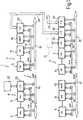
- each PN module 5comprises four active modules PE (PROCESSING ELEMENT) 31 which are the elementary computing units of the architecture and identical to one another.
- PEPROCESSING ELEMENT
- PE modules 31are connected parallel by a common line (group bus) 34 extending between a region interface 37 connected to region bus 10, and a family interface 39 connected to the respective family bus 14 to which PN module 5 is connected.
- group busgroup bus
- Each PN modulealso comprises a direct memory access (DMA) control block 41 connected to group bus 34 and which provides for emitting a number of memory location addresses as of which data is transferred. Operation of block 41 will be described in more detail later on.
- DMAdirect memory access
- each PE module 31is subdivided into two blocks 44 and 45 constituting a so-called private level and a so-called local level.
- Private block 44comprises a processor (CPU) 47, and a common communication line (private bus) 49 connected to processor 47.
- processor 47CPU 47
- common communication line 49connected to processor 47.
- Processor 47constitutes the central unit of PE module 31, and may consist of an X86-family INTEL microprocessor supplied with 32 address bits and 32 data bits.
- Communication line 49supports the data, addresses and control signals to and from processor 47.
- Block 44also comprises a coprocessor 51, e.g. a MOTOROLA DSP96002 or CYRIX 83D87, connected to private bus 49.
- a coprocessor 51e.g. a MOTOROLA DSP96002 or CYRIX 83D87, connected to private bus 49.
- Coprocessor 51provides for accelerating a number of operations which would be an "encumbrance" if performed solely by processor 47.
- Coprocessor 51may be a master/slave or slave only type. If a master/slave type, it is associated with a circuit (not shown) for converting the cycle performed by coprocessor 51 into the same cycle as processor 47, and so permitting access by coprocessor 51 to the various levels (region, family, group, local, private) of unit 3; and is associated with a coprocessor paging unit (UPC) block 58 connected to private bus 49 and communicating with coprocessor 51.
- UPCcoprocessor paging unit
- UPC block 58translates the linear addresses emitted by coprocessor 51 into physical addresses according to the memory management mechanism of processor 47, to permit coprocessor 51 to access the entire memory of system 1 using the same mechanism as processor 47.
- UPC block 58is started up by processor 47 during startup of system 1 as a whole, so that it contains all the information relative to the memory structure of unit 3 of system 1.
- UPC block 58therefore provides for translating the addresses emitted by coprocessor 51, and for generating interrupts to processor 47 whenever coprocessor 51 attempts to access an address not described in UPC block 58.
- coprocessor 51is not permitted access to system resources, and only contains the logics required for supporting operation of the system, in which case, UPC block 58 is absent, and processor 47 accesses coprocessor 51 as it would an input/output port.
- FIG. 5shows the hardware structure for supporting and connecting coprocessor 51 to the other parts of the PN module. More specifically, each PN module 5 is formed on a rectangular CSM board (printed circuit) to which a number of electronic components are SMT welded (Surface Mounting Technique).
- CSM boardprinted circuit
- SMT weldedSurface Mounting Technique
- the CSM boardalso presents one (or more) sockets Z for connection to pins P extending from the bottom face of an add-on board and forming part of an integrated circuit forming processor 47.
- the add-on boardalso supports the integrated circuit forming coprocessor 51, and the circuits forming UPC block 58.
- Private bus 49is also connected to a private RAM memory 53, and to an EPROM memory 55, more specifically a FLASH-EPROM memory, in which the operating system and startup and diagnostic programs are stored.
- RAM memory 53presents an extremely short access time permitting no-wait-cycle operation of processor 47.
- Private block 44comprises a peripheral unit 56 connected to private bus 49 and which provides for performing all the auxiliary control functions required by the PE module (e.g. timing, fault detection, etc.).
- Private block 44also comprises a general-purpose decoding (DMU) block 59 connected to private bus 49 and which provides for decoding the addresses emitted by processor 47 and/or coprocessor 51, and for generating access requests to the various levels of units 3.
- DMUgeneral-purpose decoding
- DMU block 59contains information relative to the memory mapping of unit 3 as a whole.
- DMU block 59is also connected by line 60 to a local arbiter block 61 in turn connected by line 62 to an interface 64 for connecting/separating private bus 49 to/from a line (local bus) 66 forming part of local block 45 and supporting data, addresses and control signals.
- Local block 45comprises a local RAM memory 67 connected to local bus 66 and accessible by processor 47, group bus 34, and region and family buses 10, 14.
- RAM 67constitutes the local memory of PE module 31, is shared by the private level and group level, and is accessed rapidly to permit no-wait-cycle operation of processor block 47.
- Local block 45also comprises an address generating (ADG) block 70 connected to local bus 66 and cooperating with, and generating the addresses for, RAM memory 67.
- ADGaddress generating
- Local bus 66is also connected to an interface 72 which separates local block 45 from group bus 34 for exchanging data and control signals to and from group bus 34.
- Interface 72is connected by line 74 to local arbiter block 61.
- Local arbiter block 61is also connected by line 75 to a group arbiter block 76 connected to region interface 37 and family interface 39.
- block 61controls data transfer between the private, local, group, region and family levels.
- Local arbiter block 61provides for arbitrating the access requests from processor block 47 or coprocessor 51, from group, family and region buses 34, 14, 10, and from DMA controller 41.
- block 61may receive from processor 47 over line 60:
- Block 61supplies along line 62 a signal F for connecting private bus 49 and local bus 66 via interface 64, and along line 74 a signal G for connecting local bus 66 and group bus 34 via interface 72.
- Local arbiter block 61receives and transmits along line 75 a signal H containing the access requests to and from the group level.
- Group arbiter block 76arbitrates use of group bus 34 by the four PE modules 31, of the region and family levels, and of controller 41.
- Block 41is connected to a general-purpose decoding (DMU) block 79 for decoding the addresses emitted by block 41, and for generating access requests to the various system levels.
- Block 79contains information relative to mapping of the entire memory space of the system, and is started up at the startup phase.
- DMUgeneral-purpose decoding
- Block 79is also connected to a DMA ARBITER block 81 communicating with group arbiter block 76, and which provides for controlling access to and from block 41.
- block 41may access address generating block 70 for programming it.
- block 81receives a number of signals from block 79:
- the PGM-ADG-LOC signalprovides for programming blocks 70 and identifying the memory locations as of which data is to be transferred in DMA mode.
- Module 20is composed of a standard part, identical to PE module 31 already described, and a specific input/output part.
- module 20is subdivided into two blocks 44 and 45 constituting a so-called private level and a so-called local level.
- Private block 44comprises a processor (CPU) 47, and a common communication line (private bus) 49 connected to processor 47.
- processor 47CPU 47
- common communication line 49connected to processor 47.
- Processor 47may consist, for example, of an X86-family INTEL microprocessor supplied with 32 address bits and 32 data bits.
- Communication line 49supports the data, addresses and control signals to and from processor 47.
- Block 44also comprises a coprocessor 51, e.g. a MOTOROLA DSP96002 or CYRIX 83D87, connected to private bus 49.
- a coprocessor 51e.g. a MOTOROLA DSP96002 or CYRIX 83D87, connected to private bus 49.
- Private bus 49is also connected to a private RAM memory 53, and to an EPROM memory 55, more specifically a FLASH-EPROM memory, in which the operating system and startup and diagnostic programs are stored.
- RAM memory 53presents an extremely short access time permitting no-wait-cycle operation of processor 47.
- Private block 44comprises a peripheral unit 56 connected to private bus 49 and which provides for performing all the auxiliary control functions required by the PE module (e.g. timing, fault detection, etc.).
- Private block 44comprises a coprocessor paging unit (UPC) block 58 connected to private bus 49 and communicating with coprocessor 51.
- UPCcoprocessor paging unit
- Block 58translates the linear addresses emitted by coprocessor 51 into physical addresses to permit coprocessor 51 to access the entire memory of system 1 using the same memory management structure as processor 47.
- Private block 44also comprises a general-purpose decoding (DMU) block 59 connected to private bus 49 and which provides for decoding the addresses emitted by processor 47 or coprocessor 51, and for generating access requests to the various levels of system 1.
- DMUgeneral-purpose decoding
- block 59contains information relative to the memory mapping of the system as a whole.
- Block 59is also connected by line 60 to a local arbiter block 61 in turn connected by line 62 to an interface 64 for connecting/separating private bus 49 to/from a line (local bus) 66 forming part of local block 45 and supporting data, addresses and control signals.
- a local arbiter block 61in turn connected by line 62 to an interface 64 for connecting/separating private bus 49 to/from a line (local bus) 66 forming part of local block 45 and supporting data, addresses and control signals.
- Local block 45comprises a local RAM memory 67 connected to local bus 66 and accessible by processor 47.
- RAM 67constitutes the local memory of the PE module, is shared by the private level and group level, and is accessed rapidly to permit no-wait-cycle operation of processor block 47.
- Local block 45also comprises an address generating (ADG) block 70 connected to local bus 66 and cooperating with, and generating the addresses for, RAM memory 67.
- ADGaddress generating
- Local bus 66is also connected to an interface 72 driven via line 74 by local arbiter block 61, and which separates/connects local bus 66 from/to group bus 34 for exchanging data and control signals to and from group bus 34.
- Arbiter block 61is also connected by line 75 to a group arbiter block 76 connected by respective lines 77, 78 to region interface 37 and family interface 39.
- block 61controls data transfer between the private, local, group, region and family levels.
- Local arbiter block 61provides for arbitrating the access requests from processor block 47, coprocessor 51, or group bus 34.
- block 61may receive over line 60:
- Block 61supplies along line 62 a signal F for connecting the private bus and local bus via interface 64, and along line 74 a signal G for connecting the local bus and group bus via interface 72.
- Block 61receives along line 75 a signal H containing the access requests to and from the group level.
- Module 20comprises DMA controller block 41 connected to group bus 34, and general-purpose decoding (DMU) block 79 for decoding the addresses emitted by block 41, and for generating access requests to the various system levels.
- DMUgeneral-purpose decoding
- Block 79is also connected to a DMA ARBITER block 81 communicating with group arbiter block 76, and which provides for controlling access to and from block 41.
- block 41may access address generating block 70 for programming it.
- block 81receives a number of signals from block 79:
- Data exchange module 20also comprises a line (bus) 100 extending from group bus 34 to private bus 49 to which it is connected via a separating device 101.
- Line 100also presents two separating devices 103, 104, so that it is subdivided into a first portion 100' extending between separating devices 101, 103; a second portion 100'' extending between separating devices 103, 104; and a third portion 100''' extending between device 104 and group bus 34.
- Module 20comprises an add-on arbiter block 110 input-connected to decoding (DMU) block 59 and to group arbiter block 76.
- DMUdecoding
- Block 110is output-connected to separating devices 101, 103, 104 over respective lines 111, 113, 114.
- Module 20comprises buffer memory block 120 communicating with portion 100'' of bus 100 and with an input/output channel (e.g. formed by interregional bus 24).
- Block 120provides for temporary data storage, and presents a memory size depending on the type of data exchange input/output channel employed.
- Block 120is accessible directly by processor 47 and coprocessor 51 via separating devices 101, 103, and from the architectural standpoint forms part of the private level.
- Controller block 41may access block 120 directly via group level and separating device 104, for loading/unloading the data in block 120 into local RAM memory 67 of module 20 or another system 1 module.
- Block 120cooperates with address generating block 130, which also communicates with group bus 34 and provides for locally generating the addresses for block 120 (buffer) when this is accessed in DMA mode.
- block 130synthesizes the next location address following that of the current cycle, and provides for high speed data transfer on region and family buses 10, 14.
- Block 110provides for arbitrating access requests to block 120 from private-level processor 47 (and generated by DMU block 59), and for arbitrating access requests to block 120 from the input/output channel and generated by an input/output controller block 140 connected to the input/output channel.
- Arbiter block 110generates:
- Memory module MEMT 16will now be described in detail with reference to Figure 4.
- each memory module MEMT 16comprises a data exchange line 200, similar to a group bus, connected to region bus 10 and family bus 14 by respective interface blocks 203, 204.
- interface blocks 203, 204contain the decoding functions for accessing MEMT module 16 according to the system mapping structure, which functions are programmed via region bus 10 during startup of system 1.
- Memory module MEMTcomprises a RAM memory (MEMORY ARRAY) 210 input-connected to bus 200 via the interposition of a first block FIFO IN (first in first out) 215, and having an output connected to bus 200 via the interposition of a second block FIFO OUT (first in first out) 220.
- RAM memoryMEMORY ARRAY
- Memory 210is composed of four dynamic RAM banks, each with a four Mega x 32 bit capacity.
- the first block FIFO IN 215provides for temporally decoupling a write cycle on region bus 10 or family bus 14 and a write cycle in memory 210.
- the second block FIFO OUT 220provides for temporally decoupling of a read cycle on the region or family bus and a read cycle in memory 210.
- MEMT module 16comprises an address generating block (ADG) 230 communicating with bus 200; and a DRAM CONTROLLER block 235 connected to block 230 and RAM memory 210, and which provides for addressing memory 210 as described later on.
- ADGaddress generating block
- DRAM CONTROLLER block 235connected to block 230 and RAM memory 210, and which provides for addressing memory 210 as described later on.
- Address generating block 230is also connected to an OFFSET RAM block 237 communicating with bus 200, and which causes block 230, in the course of DMA cycles (as explained in detail later on), to generate nonconsecutive addresses offset by programmable intervals.
- MEMT module 16also comprises a CYCLE CONTROL block 240 communicating with a group arbiter block 245 connected by respective lines 246, 247 to interface blocks 203, 204.
- Cycle control block 240is connected by respective control lines 250, 251, 252, 253, 254 to memory 210, in which it may perform a read/write cycle, to FIFO OUT block 220, FIFO IN block 215, DRAM controller block 235, and address generating block ADG 230.
- Memory 210is connected to an EDC block 260 for generating an error-detecting (e.g. Hamming) code for the write data. More specifically, EDC block 260 assigns to each 32-bit word stored in memory 210 a seven-bit error-detecting code created on the basis of the Hamming polynomial, and which provides for detecting and correcting one error in the 32-bit word, and for detecting (but not correcting) two (or more) errors.
- error-detectinge.g. Hamming
- Memory 210is also connected to a CHECK MEMORY block 265 containing the bit set from which to generate the codes for detecting and correcting errors in the input and output data of memory 210.
- the data in memories 210is read and scrubbed periodically (e.g. at 1 Herz frequency) to eliminate, by virtue of the Hamming code assigned to each 32-bit word, any one-bit errors occurring in the words (e.g. due to alpha particles).
- block 245 of MEMT module 16arbitrates the access requests from region bus 10 and family bus 14, and then enables cycle control block 240 which provides for performing the read/write cycles in MEMT module 16.
- cycle control block 240generates respectively:
- Figure 6shows a schematic diagram of the internal structure of memory 210, which does not necessarily correspond with the actual physical embodiment of memory 210, but serves to illustrate the particular mechanism by which memory 210 is addressed by blocks 230, 237 according to the present invention.
- memory 210may be thought of as defining a rectangular table T divided into N number of rows R1, R2, R3...Rn, each composed of K elementary storage modules in turn composed of a given number of bits, e.g. 32.
- Table Ttherefore contains N*K elementary modules, and is normally read/written in successive rows by sequentially accessing the various elementary modules in each row by means of successive addresses.
- the memoryin DMA cycles, may also be accessed in columns.
- block 230In read mode by columns, block 230 generates the address using an accumulating adder, one addend of which is programmable and consists of integer K (transposition offset) from OFFSET RAM block 237.
- each PE module in the systemmay be assigned a respective table and, hence, a respective K value for reading the table in columns.
- OFFSET RAM block 237is composed of a static RAM memory bank with a 2K x 24 bit capacity, which RAM is addressed at the input with a parameter exclusively indicating the PE module 31 performing the data read/write cycle, and supplies at the output the transposition offset K for that particular PE module 31.
- DRAM controller block 235provides for multiplexing the addresses from block 230.
- the multiprocessor system according to the present inventiontherefore employs six hierarchical levels "nested" from the elementary processing unit (processor 47 or coprocessor 51) to the system consisting of the processing unit 3 network.
- the six levelsclassed according to the extent to which they are permitted to share the common resources of the system (memories and inputs/outputs accessible directly by all the elements connected to the same bus), include: private level, local level, group level, family level, region level, and region network level.
- system 1is based on six levels, the first five of which (private-local-group-family-region) are "mapped" in the addressing space (4 Gbytes) of each processor 47.
- Each levelmay contain a variable amount of storage, so that, after supplying system 1, a system startup phase must be performed to establish the size of the memory assigned to each level.
- the startup phaseis performed by a "master" elected PE module 31 by means of the operation sequence shown in the Figure 7 block diagram.
- the sequencecommences with a block 300 which determines the amount of storage present in each family and which is represented, for a given n-th family, by two limit addresses: LBFn (Limit-Bottom-Family-n) and LTFn (Limit-Top-Family-n).
- LBFnLimit-Bottom-Family-n
- LTFnLimit-Top-Family-n
- Block 300goes on to block 310 in which the two limit addresses LBFn, LTFn defined in block 300 are programmed in family decoders (formed in family interface 39 and not shown) of family n, so that each address emitted by a processor 47 (or coprocessor 51) in the n-th family and falling within the two limits LBFn, LTFn requests access to the n-th family bus.
- family decodersformed in family interface 39 and not shown
- Block 310goes on to block 320 which, within the two family limits LTFn, LBFn defined in block 300, identifies a number of address spaces, each relative to a group in the n-th family, each contiguous to another space, and each represented, for the m-th group, by two limit addresses: LBGm (Limit-Bottom-Group-m) and LTGm (Limit-Top-Group-m).
- LBGmLimit-Bottom-Group-m
- LTGmLimit-Top-Group-m
- Block 320goes on to block 340 in which the two limit addresses LBGm, LTGm identifying the m-th group are programmed in group decoders (indicated 96 in Figure 2) of group m itself, so that each address emitted by any processor 47 (or coprocessor 51) in group m and falling within limits LBGm, LTGm requests access to the m-th group bus.
- group decodersindicated 96 in Figure 2
- Block 340goes on to block 350 which, within the two group limits LBGm, LTGm defined by block 320, and for multiprocessor modules PN only, identifies a number of address spaces, each relative to a local bus in group m, each contiguous to another space, and each represented, for the p-th local bus, by two limit addresses: LBLp (Limit-Bottom-Local-p) and LTLp (Limit-Top-Local-p).
- LBLpLimit-Bottom-Local-p
- LTLpLimit-Top-Local-p
- Block 350goes on to block 360 in which the two limit addresses LBLp, LTLp identifying local bus p are programmed in local decoders (formed by UPC block 58) of the PE module, so that each address emitted by a processor 47 in a p-th PE module and falling within limits LBLp, LTLp requests access to the p-th local bus.
- Block 360goes on to block 370 which defines the region address space, which consists of the combined address spaces of the families and is represented by two limit addresses: LBR (Limit-Bottom-Region) and LTR (Limit-Top-Region).
- LBRLimit-Bottom-Region
- LTRLimit-Top-Region
- the Figure 8 diagramshows the subdivision of the system memory effected by the above procedure.
- each PE moduleselects the level at which to perform a transaction fully automatically.
- the first five hierarchical levelstogether form the overall processing unit 3 of system 1, which is characterized by "visibility" or direct access to a given physical address space by the various mutually-cooperating PN modules 5.
- Unit 3in itself constitutes an extremely high-power system capable of real-time controlling a set of several tens of families, each family in turn consisting of several tens of multiprocessor modules PN. Power in terms of MIPS (million instructions per second) for each region may be thought of as ranging between 100 and 10000 MIPS depending on the type of processor and coprocessor used.
- the total processing power of the network system of regions 7may therefore range between over 10000 MIPS and 16 times 10000, which is far superior to that currently achievable by known systems.
- Data exchange in DMA modeinvolves a preparatory phase in which to determine the communication channel between the source and destination.
- the preparatory phaseis performed entirely by the DMA controller 41 of the PN module in which the processor 47 requesting the data exchange is located, for which purpose, DMA controller 41 is programmed by processor 47 with the physical address of the first location of the data block in the source RAM 67, with the physical address of the first location of the data block in the destination RAM 67, and with the size of the data block being transferred.
- the preparatory phasecontinues with DMA controller 41 requesting access to the hierarchical levels required for effecting the data exchange, for which purpose, block 41 employs DMU block 79 containing the system mapping structure.
- DMA controller 41requesting access to the hierarchical levels required for effecting the data exchange, for which purpose, block 41 employs DMU block 79 containing the system mapping structure.
- the above operationmakes selection of the levels at which to effect the data exchange in DMA mode automatic, i.e. invisible to the system 1 programmer.
- the data in the source local RAM 67is first transferred to a pipeline register PIP ( Figure 2) at the output of RAM 67, so that a subsequent read cycle may be performed in the source RAM 67 even before the current cycle data is fetched from the pipeline register.
- PIPpipeline register
- the data block programmed for data transferis automatically broken up into sub-blocks of four kilobytes to prevent overoccupation of the data exchange buses by DMA controller block 41.
- DMA data transfersmay be made via group level between two local RAMs 67 of two PE modules in the same PN module, in which case, to prevent conflict between various PE modules, a hardware device (traffic light) 41a of DMA controller 41 provides for assigning the group bus to only one PE module at a time.
- a hardware device (traffic light) 41a of DMA controller 41provides for assigning the group bus to only one PE module at a time.
- transfersemploy the local source and destination levels, the group level of the module containing the source local RAM, and the family level and group level of the module containing the destination local RAM.
- transfersemploy the local source and destination levels, the group level of the module containing the source local RAM, and the region level and group level of the module containing the destination local RAM.
- DMA controller 41is of great importance as regards data exchange modules 20 in which, in addition to local RAM 67, it is also permitted access to buffer memory block 120 for filling/emptying it.
- system 1presents a communication channel (group bus) common to all the PE modules 31 and which, absent in said Patent EP-226.096, permits activity within the PN module with no interference with the external environment (family and region).
- each PE module in the PN modulemay access the local RAM 67 of another PE module, and exchange data (even in DMA mode) without interacting with the other PE modules or higher family and region levels.
- each PE modulemay access its own local RAM 67 directly without interfering with the other PE modules, and may access the family and region levels while the other PE modules access their own local levels.
- System 1therefore employs coprocessor 51 openly and flexibly since each PE module 31 may employ different (commercial or custom) coprocessors by virtue of UPC block 58 translating the linear addresses emitted by coprocessor 51 into physical addresses so that the memory management of coprocessor 51 corresponds with that of processor 47.
- the particular hardware structure employed for supporting coprocessor 51also enables coprocessors of different sizes and pin arrangements to be used without altering the CSM printed circuit supporting the components forming the host module (e.g. PN module 5).
- System 1also presents a "distributed" DMA structure, i.e. each PN module 5 presents its own device (DMA controller 41) capable of supporting data exchange to and from the other system 1 modules in DMA mode.
- DMA controller 41DMA controller 41
- Such DMA transfersmay be made at various hierarchical levels of the system as demonstrated previously.
- DMA transferalways employs three pipeline stages (source pipeline register - transfer buses - destination pipeline register) thus providing for considerable decoupling of the data source and destination, and greatly reducing the access time of the exchange buses.
- MEMT module 16permits both row and column access to memory 210, which is particularly advantageous when dealing with certain types of data (such as image digitization data).
- Compulsory use of the family level for transactions between two PE modules 31 in the same familyprovides for safeguarding against deadlock situations.
- the startup phase describedpermits each processor 47 of each PE module to know the mapping structure of unit 3 from its own vantage point.
- each PE moduleselects the data exchange level automatically and fully “transparently” to the programmer.
Landscapes
- Engineering & Computer Science (AREA)
- Computer Hardware Design (AREA)
- Theoretical Computer Science (AREA)
- Physics & Mathematics (AREA)
- General Engineering & Computer Science (AREA)
- General Physics & Mathematics (AREA)
- Software Systems (AREA)
- Computing Systems (AREA)
- Multi Processors (AREA)
Description
- at least one processing unit comprising a numberof multiprocessor modules PN connected to adirect-access line to form a region level;
- said number of multiprocessor modules PN alsobeing subdivided into at least two subgroups, eachcomprising respective numbers of multiprocessor modulesPN connected to a respective direct-access line to forma family level;
- each multiprocessor module comprising a numberof active processing modules PE connected to a commondirect-access line to form a group level; and
- said group line also communicating with saidregion line and said family line.
- an ACC-RAM signal for requesting access to a RAMmemory 67 of another
PE module 31 via group level; - an ACC-REG signal for requesting access to the region level;
- an ACC-FAM signal for requesting access to thefamily level;
- an ACC-GROUP signal for requesting access to thegroup level; and
- an ACC-DMA signal for requesting access to theregisters of
DMA controller 41.
- a PGM-ADG-LOC signal for requesting access by
DMA controller 41 to address generatingblock 70 viagroup level forprogramming block 70; - an ACC-GROUP signal for requesting access to thegroup level;
- an ACC-FAM signal for requesting access to thefamily level; and
- an ACC-REG signal for requesting access to theregion level.
- an ACC-RAM signal for requesting access to localRAM memory 67;
- an ACC-REG signal for requesting access to theregion level;
- an ACC-FAM signal for requesting access to thefamily level;
- an ACC-GROUP signal for requesting access to thegroup level;
- an ACC-DMA signal for requesting access to theregisters of
DMA controller 41 at group level; and - an ACC-BUF signal for requesting access to abuffer memory block 120 (input/output buffer) describedin detail later on.
- a PGM-ADG-LOC signal for requesting access by
DMA controller 41 to block 70, forprogramming block 70; - a PGM-ADG-BUF signal for requesting access to a
block 130 addressingblock 120, forprogramming block 130; - an ACC-GROUP signal for requesting access to thegroup level;
- an ACC-FAM signal for requesting access to thefamily level; and
- an ACC-REG signal for requesting access to theregion level.
Claims (33)
- A multilevel multiprocessor systemcomprising:at least one processing unit (3) comprising anumber of multiprocessor modules PN (5) each connected to adirect-access line (10) to form a region level;said number of multiprocessor modules PN (5)also being subdivided into at least two subgroups, eachcomprising respective numbers of multiprocessor modulesPN (5) each connected to a respective direct-access line (14)to form a family level;each multiprocessor module (5) comprising anumber of active processing modules PE (31) each connected toa common direct-access line (34) to form a group level;andsaid group line (34) also being interfaced (37, 39) withsaid region line (10) and said family line (14).
- A system as claimed in Claim 1, characterizedin that it comprises a number of processing units (3)connected to one another by data receiving andtransmitting means (24) to form a region network.
- A system as claimed in Claim 1 or 2,characterized in that each said processing module PE(31) comprises at least one processor (47) and privatememory means (53) associated with said processor (47),said processor (47) and said private memory means (53)being connected to a private communication line (49) defining a private level;said processing module PE (31) also comprising alocal communication line (66) separable/connectablefrom/to said private line (49) and communicating withsaid group line (34).
- A system as claimed in Claim 3, characterizedin that it comprises coprocessors (51) associated withsaid processors (47) and communicating with said privateline (49);said coprocessors (51) assisting processing bysaid processors (47).
- A system as claimed in Claim 4, characterizedin that it comprises UPC (coprocessor paging unit) means(58) connected to said private line (49) and cooperatingwith said coprocessors (51);said UPC means (58) translating the linearaddresses emitted by said coprocessors (51) intophysical addresses to permit access by the coprocessors(51) to the memory of said system (1).
- A system as claimed in Claim 3, 4 or 5,characterized in that each said processing module PE(31) comprises first RAM type private memory means (53)communicating with said private line (49); andsecond EPROM type memory means (55) communicatingwith said private line (49) and supporting an operatingsystem and/or startup and diagnostic programs.
- A system as claimed in one of the foregoingClaims from 4 to 6, wherein each multiprocessor module PN (5) is formed on a main board (CSM) supporting anumber of electronic components; characterized in thatsaid main board (CSM) presents at least one socket (Z)for receiving the pins (P) of an integrated circuitforming said processor (47);said integrated circuit forming said processor(47) and an integrated circuit forming said coprocessor(51) being supported on an additional (ADD-ON) boardseparate from said main board (CSM).
- A system as claimed in one of the foregoingClaims from 3 to 7, characterized in that each saidprocessing module PE (31) comprises first decoding meansDMU (59) for receiving the connection requests emittedby said processor (47) and/or said coprocessor (51) foraccess to said private line (49), to said local line(66) and to said group line (34);said first decoding means (59) cooperating withlocal arbitrating means (61) for controlling connectionbetween said private line (49), said local line (66) andsaid group line (34) according to a request from saidfirst decoding means (59).
- A system as claimed in Claim 8, characterizedin that it comprises:first interface means (64) interposed between saidprivate line (49) and said local line (66); andsecond interface means (72) interposed betweensaid local line (66) and said group line (34);said local arbitrating means (61), on the basis of the command generated by said first decoding means DMU(59), supplying said first (64) and second (72)interface means with respective signals (F,G) forconnecting said private line (49) and said local line(66) via said first interface means (64), and connectingsaid local line (66) and said group line (34) via saidsecond interface means (72).
- A system as claimed in Claim 9, characterizedin that it comprises:third interface means (37) interposed between saidgroup line (34) and said region line (10); andfourth interface means (39) interposed betweensaid group line (34) and said family line (14);said processing module PE (31) also comprisinggroup arbitrating means (76) cooperating with said localarbitrating means (61) and controlling said third (37)and fourth (39) interface means.
- A system as claimed in one of the foregoingClaims from 2 to 10, characterized in that each saidprocessing module PE (31) comprises RAM local memorymeans (67) connected to said local line (66) andaccessible by said processor (47).
- A system as claimed in Claim 11, characterizedin that it comprises addressing means ADG (70) connectedto said local line (66) and cooperating with said localmemory means (67), for generating the addresses for saidlocal memory (67).
- A system as claimed in any one of the foregoing Claims, characterized in that each saidmultiprocessor module PN (5) presents direct memoryaccess DMA controller means (41) communicating with saidgroup line (34);said DMA controller means (41) selecting addressesof memory locations as of which to transfer/receive adata block.
- A system as claimed in Claim 13, characterizedin that it comprises second decoding means DMU (79)cooperating with said DMA controller means (41), andwhich decode the signals emitted by said controllermeans (41), for generating the access requests to thevarious hierarchical levels of the system;said second decoding means (79) containinginformation relative to the mapping structure of theentire memory space of said system (1).
- A system as claimed in Claim 14 dependent onClaims 10 and 12, characterized in that said seconddecoding means (79) cooperate with DMA arbitrating means(81) communicating with said group arbitrating means(76), for controlling access to and from said addressingmeans ADG (70) for programming said addressing means(70).
- A system as claimed in Claim 15, characterizedin that said second decoding means (79) supply said DMAarbitrating means (81) with a number of signals:a PGM-ADG-LOC signal for requesting access bysaid DMA controller means (41) to said addressing means ADG (70) via group level, for programming saidaddressing means ADG (70) to select the memory locationas of which to transfer/receive a data block;an ACC-GROUP signal for requesting access to thegroup level;an ACC-FAM signal for requesting access to thefamily level; andan ACC-REG signal for requesting access to theregion level.
- A system as claimed in one of the foregoingClaims from 8 to 16 dependent on Claim 11, characterizedin that said local arbitrating means (61) receive fromsaid first decoding means (59):an ACC-RAM signal for requesting access to saidlocal memory;an ACC-REG signal for requesting access to theregion level;an ACC-FAM signal for requesting access to thefamily level;an ACC-GROUP signal for requesting access to thegroup level; andan ACC-DMA signal for requesting access to theregisters of said DMA controller means (41).
- A system as claimed in any one of theforegoing Claims, characterized in that it comprises atleast one memory module MEMT (16) connected between saidfamily line (14) and said region line (10); said memorymodule MEMT (16) being directly accessible to and from said family line (14) and said region line (10).
- A system as claimed in Claim 16, characterizedin that said memory module MEMT (16) comprises:a data exchange line (200) communicating with theregion line (10) and the family line (14) via respectiveregion and family interfaces (203, 204);a RAM memory (210) addressable in rows andcolumns;first temporary data accumulating means FIFO IN(215) interposed between said data exchange line (200)and a data input of said RAM memory (210); andsecond temporary data accumulating means FIFO OUT(220) interposed between said data exchange line (200)and a data output of said RAM memory (210).
- A system as claimed in Claim 18 or 19,characterized in that said memory module (16) comprises:address generating means (230) connected to OFFSETRAM means (237); andmemory controlling means (235) interposed betweensaid address generating means (230) and said RAM memory(210);said memory (210) defining a data accumulatingstructure comprising at least one rectangular table (T)divisible into N number of rows R1, R2, R3...Rn, eachcomposed of K elementary storage modules;said address generating means (230) obtainingaccess to said table (T) in columns by sequentiallyadding to the address of the first addressed storage module (C1) an integer K (transposition offset)generated by said OFFSET RAM means (237) and equal tothe number K of elementary modules per row.
- A system as claimed in Claim 20, characterizedin that said memory module (16) defines a dataaccumulation structure composed of a number of tables(T, T1,,,Tn) with rows of different lengths;each said table (T, T1...Tn) being associated witha respective processing module PE (31);said address generating means (230) obtainingaccess by columns to said tables (T, T1...Tn) usingdifferent integers (K, K1...Kn) (transposition offsets)generated by said OFFSET RAM means (237).
- A system as claimed in one of the foregoingClaims from 19 to 21, characterized in that said memorymodule MEMT (16) comprises:cycle control means (240) for controlling said RAMmemory (210), said first temporary data accumulatingmeans (215) and said second temporary data accumulatingmeans (220); andgroup arbitrating means (245) communicating withsaid cycle control means (240) and said region andfamily interfaces (203, 204);said group arbitrating means (245) arbitratingaccess requests from the region line (10) and familyline (14); and, at the end of the arbitration phase,enabling said cycle control means (240) to perform theread/write cycles in said MEMT module (16).
- A system as claimed in Claim 22 dependent onClaim 20, characterized in that said cycle control means(240) generate respectively:a WE signal for write-enabling the memory (210);an EFO signal for writing the output data from thememory (210) in said second temporary accumulating meansFIFO OUT (220);an EFI signal for enabling reading of the data insaid first temporary accumulating means FIFO IN (215)and supply of said data to the memory (210);an EDC signal for enabling said address generatingmeans (230); andan EDA signal for enabling said memory controllingmeans (235).
- A system as claimed in any one of theforegoing Claims from 18 to 23, characterized in thatsaid memory (210) is connected to an EDC block (250)which, for the write data, generates an error-detectingcode, in particular a Hamming code, fordetecting/correcting at least one data error.
- A system as claimed in any one of theforegoing Claims from 18 to 24, characterized in thatsaid RAM memory (210) is connected to a CHECK MEMORYblock (265) for generating the error-detecting codes fordetecting and correcting errors in the input and outputdata of the memory (210).
- A system as claimed in any one of theforegoing Claims from 2 to 25, characterized in that it comprises at least one data exchange module (20)connected between said family line (14) and said regionline (10); said data exchange module (20) being directlyaccessible to and from said family line (14), saidregion line (10) and said data receiving andtransmitting means (24).
- A system as claimed in Claim 26, characterizedin that said data exchange module (20) comprises:at least one processor (47) communicating with acommon communication line (49) defining a private level;a second common communication line (66)communicating with said private line (49) via firstinterface means (64) and defining a local level;local memory means (67) communicating with saidlocal line (66);a third common communication line (34)communicating with said local line (66) via secondinterface means (72) and defining a group level;said group line (34) communicating with saidfamily line (14) and said region line (10);a fourth common communication line (100) for dataexchange, communicating with said private line (49) andwith said group line (34) via respective third andfourth interface means (101, 104); andbuffer memory means (120) communicating with saiddata exchange line (100) and said data receiving andtransmitting means (24);said buffer memory means (120) temporarily storing data exchanged to and from said data exchange module(20).
- A system as claimed in Claim 27, characterizedin that said data exchange module (20) comprises:addressing means (130) communicating with saidgroup line (34) and said buffer memory means (120);said addressing means (130) generating addressesfor said buffer memory means (120).
- A system as claimed in Claim 28, characterizedin that said data exchange module (20) comprises:I/O arbitrating means (110) communicating at theinput with third decoding means (59) connected to saidprivate line (49);said I/O arbitrating means (110) communicating atleast with said third and fourth interfaces (101, 104)and with a fifth interface (150) cooperating with saiddata transmitting means (24);said I/O arbitrating means (110) arbitratingaccess requests to said data exchange module (20) fromsaid private level, from said group level and from saiddata transmitting means (24).
- A system as claimed in any one of theforegoing Claims from 27 to 29, characterized in thateach said data exchange module (20) comprises:direct memory access DMA controller means (41)communicating with said group line (34);fourth decoding means DMU cooperating with saidDMA controller means (41) and which decode the addresses emitted by said DMA controller means (41), forgenerating access requests to the various system levels;said fourth decoding means DMU (79) processing anumber of signals including at least:a PGM-ADG-LOC signal for requesting access bysaid DMA controller means (41) to an address generatingblock (70) connected to said local memory (67), forprogramming said local memory (67) and selecting thememory location as of which to transfer/receive a datablock;an ACC-GROUP signal for requesting access tosaid group level (49);a PGM-ADG-BUF signal for requesting access tosaid means (130) addressing said buffer memory means(120);an ACC-FAM signal for requesting access to thefamily level; andan ACC-REG signal for requesting access to theregion level.
- A system as claimed in any one of theforegoing Claims from 4 to 30, characterized in that itcomprises startup means (31) for performing, upon supplyof said system (1), a system startup phase fordetermining the size of the memory assignable to eachregion level, family level, group level and local level.
- A system as claimed in Claim 31, characterizedin that said startup means comprise:first means (300) for determining the amount of storage in each family; which amount of storage isrepresented, for any given n-th family, by two limitaddresses LBFn (Limit-Bottom-Family-n) and LTFn(Limit-Top-Family-n);second means (310) wherein the two limit addressesLBFn, LTFn defined by said first means (300) areprogrammed in decoders (39) of family n, so that anyaddress emitted by a processor (47) (or coprocessor 51)in the n-th family and falling within said two limitsLBFn, LTFn requests access to the n-th family bus;third means (320) which, within the two familylimits LTFn, LBFn defined by said first means (300),identify a number of address spaces, each relative to agroup in the n-th family, each contiguous to anotherspace, and each represented for the m-th group by twolimit addresses LBGm (Limit-Bottom-Group-m) and LTGm(Limit-Top-Group-m);fourth means (340) wherein the two limit addressesLBGm, LTGm identifying the m-th group are programmed indecoders (96) of group m, so that any address emitted byany processor (47) or coprocessor (51) in group m andfalling within limits LBGm, LTGm requests access to them-th group bus;fifth means (350) which, within the two grouplimits LBGm, LTGm defined by said third means (320),identify, for the multiprocessor modules PN (5) only, anumber of address spaces, each relative to a local busin group m, each contiguous to another space, and each represented, for the p-th local bus, by two limitaddresses LBLp (Limit-Bottom-local-p) and LTLp(Limit-Top-Local-p);sixth means (360) wherein the two limit addressesLBLp, LTLp identifying the local bus p are programmed indecoders (58) of the module PE, so that each addressemitted by a processor (47) in the p-th module PE andfalling within limits LBLp, LTLp requests access to thep-th local bus;seventh means (370) for defining the overalladdress space of a region, which space consists of thecombined address spaces of the families, and is definedby two limit addresses LBR (Limit-Bottom-Region) and LTR(Limit-Top-Region).
- A system as claimed in any one of theforegoing Claims, characterized in that eachmultiprocessor module PN (5) preferentially employs saidfamily line (14) for data exchange with anothermultiprocessor module PN (5) in the same family.
Applications Claiming Priority (2)
| Application Number | Priority Date | Filing Date | Title |
|---|---|---|---|
| ITTO930428AIT1260848B (en) | 1993-06-11 | 1993-06-11 | MULTIPROCESSOR SYSTEM |
| ITTO930428 | 1993-06-11 |
Publications (3)
| Publication Number | Publication Date |
|---|---|
| EP0628917A2 EP0628917A2 (en) | 1994-12-14 |
| EP0628917A3 EP0628917A3 (en) | 1995-08-09 |
| EP0628917B1true EP0628917B1 (en) | 2000-05-03 |
Family
ID=11411555
Family Applications (1)
| Application Number | Title | Priority Date | Filing Date |
|---|---|---|---|
| EP94108884AExpired - LifetimeEP0628917B1 (en) | 1993-06-11 | 1994-06-09 | Multiprocessor system |
Country Status (4)
| Country | Link |
|---|---|
| US (1) | US5586258A (en) |
| EP (1) | EP0628917B1 (en) |
| DE (1) | DE69424221D1 (en) |
| IT (1) | IT1260848B (en) |
Cited By (34)
| Publication number | Priority date | Publication date | Assignee | Title |
|---|---|---|---|---|
| US6968452B2 (en) | 1997-02-08 | 2005-11-22 | Pact Xpp Technologies Ag | Method of self-synchronization of configurable elements of a programmable unit |
| US6990555B2 (en) | 2001-01-09 | 2006-01-24 | Pact Xpp Technologies Ag | Method of hierarchical caching of configuration data having dataflow processors and modules having two- or multidimensional programmable cell structure (FPGAs, DPGAs, etc.) |
| US7003660B2 (en) | 2000-06-13 | 2006-02-21 | Pact Xpp Technologies Ag | Pipeline configuration unit protocols and communication |
| US7010667B2 (en) | 1997-02-11 | 2006-03-07 | Pact Xpp Technologies Ag | Internal bus system for DFPS and units with two- or multi-dimensional programmable cell architectures, for managing large volumes of data with a high interconnection complexity |
| US7028107B2 (en) | 1996-12-27 | 2006-04-11 | Pact Xpp Technologies Ag | Process for automatic dynamic reloading of data flow processors (DFPS) and units with two- or three- dimensional programmable cell architectures (FPGAS, DPGAS, and the like) |
| US7036036B2 (en) | 1997-02-08 | 2006-04-25 | Pact Xpp Technologies Ag | Method of self-synchronization of configurable elements of a programmable module |
| US7174443B1 (en) | 1996-12-20 | 2007-02-06 | Pact Xpp Technologies Ag | Run-time reconfiguration method for programmable units |
| US7210129B2 (en) | 2001-08-16 | 2007-04-24 | Pact Xpp Technologies Ag | Method for translating programs for reconfigurable architectures |
| US7237087B2 (en) | 1996-12-09 | 2007-06-26 | Pact Xpp Technologies Ag | Reconfigurable multidimensional array processor allowing runtime reconfiguration of selected individual array cells |
| US7266725B2 (en) | 2001-09-03 | 2007-09-04 | Pact Xpp Technologies Ag | Method for debugging reconfigurable architectures |
| US7394284B2 (en) | 2002-09-06 | 2008-07-01 | Pact Xpp Technologies Ag | Reconfigurable sequencer structure |
| US7434191B2 (en) | 2001-09-03 | 2008-10-07 | Pact Xpp Technologies Ag | Router |
| US7444531B2 (en) | 2001-03-05 | 2008-10-28 | Pact Xpp Technologies Ag | Methods and devices for treating and processing data |
| US7577822B2 (en) | 2001-12-14 | 2009-08-18 | Pact Xpp Technologies Ag | Parallel task operation in processor and reconfigurable coprocessor configured based on information in link list including termination information for synchronization |
| US7581076B2 (en) | 2001-03-05 | 2009-08-25 | Pact Xpp Technologies Ag | Methods and devices for treating and/or processing data |
| US7595659B2 (en) | 2000-10-09 | 2009-09-29 | Pact Xpp Technologies Ag | Logic cell array and bus system |
| US7650448B2 (en) | 1996-12-20 | 2010-01-19 | Pact Xpp Technologies Ag | I/O and memory bus system for DFPS and units with two- or multi-dimensional programmable cell architectures |
| US7657877B2 (en) | 2001-06-20 | 2010-02-02 | Pact Xpp Technologies Ag | Method for processing data |
| US7657861B2 (en) | 2002-08-07 | 2010-02-02 | Pact Xpp Technologies Ag | Method and device for processing data |
| US7822881B2 (en) | 1996-12-27 | 2010-10-26 | Martin Vorbach | Process for automatic dynamic reloading of data flow processors (DFPs) and units with two- or three-dimensional programmable cell architectures (FPGAs, DPGAs, and the like) |
| US7844796B2 (en) | 2001-03-05 | 2010-11-30 | Martin Vorbach | Data processing device and method |
| US8058899B2 (en) | 2000-10-06 | 2011-11-15 | Martin Vorbach | Logic cell array and bus system |
| US8127061B2 (en) | 2002-02-18 | 2012-02-28 | Martin Vorbach | Bus systems and reconfiguration methods |
| US8156284B2 (en) | 2002-08-07 | 2012-04-10 | Martin Vorbach | Data processing method and device |
| US8230411B1 (en) | 1999-06-10 | 2012-07-24 | Martin Vorbach | Method for interleaving a program over a plurality of cells |
| US8250503B2 (en) | 2006-01-18 | 2012-08-21 | Martin Vorbach | Hardware definition method including determining whether to implement a function as hardware or software |
| US8281108B2 (en) | 2002-01-19 | 2012-10-02 | Martin Vorbach | Reconfigurable general purpose processor having time restricted configurations |
| US8686475B2 (en) | 2001-09-19 | 2014-04-01 | Pact Xpp Technologies Ag | Reconfigurable elements |
| US8686549B2 (en) | 2001-09-03 | 2014-04-01 | Martin Vorbach | Reconfigurable elements |
| US8812820B2 (en) | 2003-08-28 | 2014-08-19 | Pact Xpp Technologies Ag | Data processing device and method |
| US8819505B2 (en) | 1997-12-22 | 2014-08-26 | Pact Xpp Technologies Ag | Data processor having disabled cores |
| US8869121B2 (en) | 2001-08-16 | 2014-10-21 | Pact Xpp Technologies Ag | Method for the translation of programs for reconfigurable architectures |
| US8914590B2 (en) | 2002-08-07 | 2014-12-16 | Pact Xpp Technologies Ag | Data processing method and device |
| US9037807B2 (en) | 2001-03-05 | 2015-05-19 | Pact Xpp Technologies Ag | Processor arrangement on a chip including data processing, memory, and interface elements |
Families Citing this family (12)
| Publication number | Priority date | Publication date | Assignee | Title |
|---|---|---|---|---|
| US6212606B1 (en)* | 1998-10-13 | 2001-04-03 | Compaq Computer Corporation | Computer system and method for establishing a standardized shared level for each storage unit |
| US6973559B1 (en)* | 1999-09-29 | 2005-12-06 | Silicon Graphics, Inc. | Scalable hypercube multiprocessor network for massive parallel processing |
| JP4783527B2 (en) | 2001-01-31 | 2011-09-28 | 株式会社ガイア・システム・ソリューション | Data processing system, data processing apparatus, and control method thereof |
| AU2002254921A1 (en)* | 2001-03-05 | 2002-09-19 | Pact Informationstechnologie Gmbh | Methods and devices for treating and processing data |
| JP4865960B2 (en) | 2001-06-25 | 2012-02-01 | 株式会社ガイア・システム・ソリューション | Data processing apparatus and control method thereof |
| US6993674B2 (en) | 2001-12-27 | 2006-01-31 | Pacific Design, Inc. | System LSI architecture and method for controlling the clock of a data processing system through the use of instructions |
| US6959372B1 (en) | 2002-02-19 | 2005-10-25 | Cogent Chipware Inc. | Processor cluster architecture and associated parallel processing methods |
| US7085866B1 (en) | 2002-02-19 | 2006-08-01 | Hobson Richard F | Hierarchical bus structure and memory access protocol for multiprocessor systems |
| RU2397538C1 (en)* | 2008-12-25 | 2010-08-20 | ООО Научно-исследовательский центр супер-ЭВМ и нейрокомпьютеров | Multiprocessor module |
| RU2402807C1 (en)* | 2009-05-04 | 2010-10-27 | Федеральное Государственное Унитарное Предприятие "Государственный Рязанский Приборный Завод" | Digital signal processing device |
| US20120096292A1 (en)* | 2010-10-15 | 2012-04-19 | Mosaid Technologies Incorporated | Method, system and apparatus for multi-level processing |
| RU2623806C1 (en)* | 2016-06-07 | 2017-06-29 | Акционерное общество Научно-производственный центр "Электронные вычислительно-информационные системы" (АО НПЦ "ЭЛВИС") | Method and device of processing stereo images |
Family Cites Families (8)
| Publication number | Priority date | Publication date | Assignee | Title |
|---|---|---|---|---|
| US4130865A (en)* | 1974-06-05 | 1978-12-19 | Bolt Beranek And Newman Inc. | Multiprocessor computer apparatus employing distributed communications paths and a passive task register |
| DE3276916D1 (en)* | 1981-09-18 | 1987-09-10 | Rovsing As Christian | Multiprocessor computer system |
| US4485438A (en)* | 1982-06-28 | 1984-11-27 | Myrmo Erik R | High transfer rate between multi-processor units |
| IT1184015B (en)* | 1985-12-13 | 1987-10-22 | Elsag | MULTI-PROCESSOR SYSTEM WITH MULTIPLE HIERARCHICAL LEVELS |
| US4734865A (en)* | 1986-01-28 | 1988-03-29 | Bell & Howell Company | Insertion machine with audit trail and command protocol |
| US4942575A (en)* | 1988-06-17 | 1990-07-17 | Modular Computer Systems, Inc. | Error connection device for parity protected memory systems |
| US4912633A (en)* | 1988-10-24 | 1990-03-27 | Ncr Corporation | Hierarchical multiple bus computer architecture |
| DE69231451T2 (en)* | 1991-03-11 | 2001-05-10 | Mips Technologies,Inc. | Backwards compatible computer architecture with extended word widths and address space |
- 1993
- 1993-06-11ITITTO930428Apatent/IT1260848B/enactiveIP Right Grant
- 1994
- 1994-06-09DEDE69424221Tpatent/DE69424221D1/ennot_activeExpired - Lifetime
- 1994-06-09EPEP94108884Apatent/EP0628917B1/ennot_activeExpired - Lifetime
- 1994-06-13USUS08/258,759patent/US5586258A/ennot_activeExpired - Fee Related
Cited By (65)
| Publication number | Priority date | Publication date | Assignee | Title |
|---|---|---|---|---|
| US7822968B2 (en) | 1996-12-09 | 2010-10-26 | Martin Vorbach | Circuit having a multidimensional structure of configurable cells that include multi-bit-wide inputs and outputs |
| US7565525B2 (en) | 1996-12-09 | 2009-07-21 | Pact Xpp Technologies Ag | Runtime configurable arithmetic and logic cell |
| US8156312B2 (en) | 1996-12-09 | 2012-04-10 | Martin Vorbach | Processor chip for reconfigurable data processing, for processing numeric and logic operations and including function and interconnection control units |
| US7237087B2 (en) | 1996-12-09 | 2007-06-26 | Pact Xpp Technologies Ag | Reconfigurable multidimensional array processor allowing runtime reconfiguration of selected individual array cells |
| US7650448B2 (en) | 1996-12-20 | 2010-01-19 | Pact Xpp Technologies Ag | I/O and memory bus system for DFPS and units with two- or multi-dimensional programmable cell architectures |
| US7899962B2 (en) | 1996-12-20 | 2011-03-01 | Martin Vorbach | I/O and memory bus system for DFPs and units with two- or multi-dimensional programmable cell architectures |
| US7174443B1 (en) | 1996-12-20 | 2007-02-06 | Pact Xpp Technologies Ag | Run-time reconfiguration method for programmable units |
| US8195856B2 (en) | 1996-12-20 | 2012-06-05 | Martin Vorbach | I/O and memory bus system for DFPS and units with two- or multi-dimensional programmable cell architectures |
| US7822881B2 (en) | 1996-12-27 | 2010-10-26 | Martin Vorbach | Process for automatic dynamic reloading of data flow processors (DFPs) and units with two- or three-dimensional programmable cell architectures (FPGAs, DPGAs, and the like) |
| US7028107B2 (en) | 1996-12-27 | 2006-04-11 | Pact Xpp Technologies Ag | Process for automatic dynamic reloading of data flow processors (DFPS) and units with two- or three- dimensional programmable cell architectures (FPGAS, DPGAS, and the like) |
| USRE45109E1 (en) | 1997-02-08 | 2014-09-02 | Pact Xpp Technologies Ag | Method of self-synchronization of configurable elements of a programmable module |
| USRE44383E1 (en) | 1997-02-08 | 2013-07-16 | Martin Vorbach | Method of self-synchronization of configurable elements of a programmable module |
| US7036036B2 (en) | 1997-02-08 | 2006-04-25 | Pact Xpp Technologies Ag | Method of self-synchronization of configurable elements of a programmable module |
| USRE44365E1 (en) | 1997-02-08 | 2013-07-09 | Martin Vorbach | Method of self-synchronization of configurable elements of a programmable module |
| US6968452B2 (en) | 1997-02-08 | 2005-11-22 | Pact Xpp Technologies Ag | Method of self-synchronization of configurable elements of a programmable unit |
| USRE45223E1 (en) | 1997-02-08 | 2014-10-28 | Pact Xpp Technologies Ag | Method of self-synchronization of configurable elements of a programmable module |
| US7010667B2 (en) | 1997-02-11 | 2006-03-07 | Pact Xpp Technologies Ag | Internal bus system for DFPS and units with two- or multi-dimensional programmable cell architectures, for managing large volumes of data with a high interconnection complexity |
| US8819505B2 (en) | 1997-12-22 | 2014-08-26 | Pact Xpp Technologies Ag | Data processor having disabled cores |
| US8468329B2 (en) | 1999-02-25 | 2013-06-18 | Martin Vorbach | Pipeline configuration protocol and configuration unit communication |
| US8312200B2 (en) | 1999-06-10 | 2012-11-13 | Martin Vorbach | Processor chip including a plurality of cache elements connected to a plurality of processor cores |
| US8726250B2 (en) | 1999-06-10 | 2014-05-13 | Pact Xpp Technologies Ag | Configurable logic integrated circuit having a multidimensional structure of configurable elements |
| US8230411B1 (en) | 1999-06-10 | 2012-07-24 | Martin Vorbach | Method for interleaving a program over a plurality of cells |
| US8301872B2 (en) | 2000-06-13 | 2012-10-30 | Martin Vorbach | Pipeline configuration protocol and configuration unit communication |
| US7003660B2 (en) | 2000-06-13 | 2006-02-21 | Pact Xpp Technologies Ag | Pipeline configuration unit protocols and communication |
| US8471593B2 (en) | 2000-10-06 | 2013-06-25 | Martin Vorbach | Logic cell array and bus system |
| US8058899B2 (en) | 2000-10-06 | 2011-11-15 | Martin Vorbach | Logic cell array and bus system |
| US9047440B2 (en) | 2000-10-06 | 2015-06-02 | Pact Xpp Technologies Ag | Logical cell array and bus system |
| US7595659B2 (en) | 2000-10-09 | 2009-09-29 | Pact Xpp Technologies Ag | Logic cell array and bus system |
| US6990555B2 (en) | 2001-01-09 | 2006-01-24 | Pact Xpp Technologies Ag | Method of hierarchical caching of configuration data having dataflow processors and modules having two- or multidimensional programmable cell structure (FPGAs, DPGAs, etc.) |
| US7581076B2 (en) | 2001-03-05 | 2009-08-25 | Pact Xpp Technologies Ag | Methods and devices for treating and/or processing data |
| US8312301B2 (en) | 2001-03-05 | 2012-11-13 | Martin Vorbach | Methods and devices for treating and processing data |
| US8099618B2 (en) | 2001-03-05 | 2012-01-17 | Martin Vorbach | Methods and devices for treating and processing data |
| US9075605B2 (en) | 2001-03-05 | 2015-07-07 | Pact Xpp Technologies Ag | Methods and devices for treating and processing data |
| US8145881B2 (en) | 2001-03-05 | 2012-03-27 | Martin Vorbach | Data processing device and method |
| US9037807B2 (en) | 2001-03-05 | 2015-05-19 | Pact Xpp Technologies Ag | Processor arrangement on a chip including data processing, memory, and interface elements |
| US7844796B2 (en) | 2001-03-05 | 2010-11-30 | Martin Vorbach | Data processing device and method |
| US7444531B2 (en) | 2001-03-05 | 2008-10-28 | Pact Xpp Technologies Ag | Methods and devices for treating and processing data |
| US7657877B2 (en) | 2001-06-20 | 2010-02-02 | Pact Xpp Technologies Ag | Method for processing data |
| US7210129B2 (en) | 2001-08-16 | 2007-04-24 | Pact Xpp Technologies Ag | Method for translating programs for reconfigurable architectures |
| US8869121B2 (en) | 2001-08-16 | 2014-10-21 | Pact Xpp Technologies Ag | Method for the translation of programs for reconfigurable architectures |
| US7840842B2 (en) | 2001-09-03 | 2010-11-23 | Martin Vorbach | Method for debugging reconfigurable architectures |
| US8686549B2 (en) | 2001-09-03 | 2014-04-01 | Martin Vorbach | Reconfigurable elements |
| US7266725B2 (en) | 2001-09-03 | 2007-09-04 | Pact Xpp Technologies Ag | Method for debugging reconfigurable architectures |
| US8209653B2 (en) | 2001-09-03 | 2012-06-26 | Martin Vorbach | Router |
| US7434191B2 (en) | 2001-09-03 | 2008-10-07 | Pact Xpp Technologies Ag | Router |
| US8069373B2 (en) | 2001-09-03 | 2011-11-29 | Martin Vorbach | Method for debugging reconfigurable architectures |
| US8407525B2 (en) | 2001-09-03 | 2013-03-26 | Pact Xpp Technologies Ag | Method for debugging reconfigurable architectures |
| US8429385B2 (en) | 2001-09-03 | 2013-04-23 | Martin Vorbach | Device including a field having function cells and information providing cells controlled by the function cells |
| US7480825B2 (en) | 2001-09-03 | 2009-01-20 | Pact Xpp Technologies Ag | Method for debugging reconfigurable architectures |
| US8686475B2 (en) | 2001-09-19 | 2014-04-01 | Pact Xpp Technologies Ag | Reconfigurable elements |
| US7577822B2 (en) | 2001-12-14 | 2009-08-18 | Pact Xpp Technologies Ag | Parallel task operation in processor and reconfigurable coprocessor configured based on information in link list including termination information for synchronization |
| US8281108B2 (en) | 2002-01-19 | 2012-10-02 | Martin Vorbach | Reconfigurable general purpose processor having time restricted configurations |
| US8127061B2 (en) | 2002-02-18 | 2012-02-28 | Martin Vorbach | Bus systems and reconfiguration methods |
| US7657861B2 (en) | 2002-08-07 | 2010-02-02 | Pact Xpp Technologies Ag | Method and device for processing data |
| US8281265B2 (en) | 2002-08-07 | 2012-10-02 | Martin Vorbach | Method and device for processing data |
| US8914590B2 (en) | 2002-08-07 | 2014-12-16 | Pact Xpp Technologies Ag | Data processing method and device |
| US8156284B2 (en) | 2002-08-07 | 2012-04-10 | Martin Vorbach | Data processing method and device |
| US8310274B2 (en) | 2002-09-06 | 2012-11-13 | Martin Vorbach | Reconfigurable sequencer structure |
| US8803552B2 (en) | 2002-09-06 | 2014-08-12 | Pact Xpp Technologies Ag | Reconfigurable sequencer structure |
| US7602214B2 (en) | 2002-09-06 | 2009-10-13 | Pact Xpp Technologies Ag | Reconfigurable sequencer structure |
| US7394284B2 (en) | 2002-09-06 | 2008-07-01 | Pact Xpp Technologies Ag | Reconfigurable sequencer structure |
| US7782087B2 (en) | 2002-09-06 | 2010-08-24 | Martin Vorbach | Reconfigurable sequencer structure |
| US7928763B2 (en) | 2002-09-06 | 2011-04-19 | Martin Vorbach | Multi-core processing system |
| US8812820B2 (en) | 2003-08-28 | 2014-08-19 | Pact Xpp Technologies Ag | Data processing device and method |
| US8250503B2 (en) | 2006-01-18 | 2012-08-21 | Martin Vorbach | Hardware definition method including determining whether to implement a function as hardware or software |
Also Published As
| Publication number | Publication date |
|---|---|
| DE69424221D1 (en) | 2000-06-08 |
| ITTO930428A1 (en) | 1994-12-11 |
| IT1260848B (en) | 1996-04-23 |
| US5586258A (en) | 1996-12-17 |
| ITTO930428A0 (en) | 1993-06-11 |
| EP0628917A2 (en) | 1994-12-14 |
| EP0628917A3 (en) | 1995-08-09 |
Similar Documents
| Publication | Publication Date | Title |
|---|---|---|
| EP0628917B1 (en) | Multiprocessor system | |
| US5247629A (en) | Multiprocessor system with global data replication and two levels of address translation units | |
| EP0380855B1 (en) | Memory configuration for use with means for interfacing a system control unit for a multi-processor system with the system main memory | |
| US5146607A (en) | Method and apparatus for sharing information between a plurality of processing units | |
| US5499346A (en) | Bus-to-bus bridge for a multiple bus information handling system that optimizes data transfers between a system bus and a peripheral bus | |
| US5247673A (en) | Multiprocessor system having distributed shared resources and dynamic global data replication | |
| US5040153A (en) | Addressing multiple types of memory devices | |
| US20090119443A1 (en) | Methods for program directed memory access patterns | |
| EP0280251B1 (en) | Shared memory controller arrangement | |
| JPH05265971A (en) | Computer system, and integrated single-chip central processor using the same | |
| JPS60114953A (en) | Computer unit employing address translation | |
| JPH05158890A (en) | Multiprocessor and data processing system and operating method thereof | |
| US5060186A (en) | High-capacity memory having extended addressing capacity in a multiprocessing system | |
| EP0509994B1 (en) | Centralized reference and change table for a multiprocessor virtual memory system | |
| JPS61275946A (en) | Cash mmu system | |
| EP0532690B1 (en) | Method and apparatus for managing page zero memory accesses in a multi-processor system | |
| US6704820B1 (en) | Unified cache port consolidation | |
| EP0251686B1 (en) | Method and apparatus for sharing information between a plurality of processing units | |
| AU633898B2 (en) | Method and means for interfacing a system control unit for a multi-processor system with the system main memory | |
| JP3643601B2 (en) | Information processing device | |
| Maenner et al. | A general-purpose multi-micro-system with high fault-tolerance and unlimited system-capacity | |
| WO1992005486A1 (en) | Method and means for error checking of dram-control signals between system modules | |
| Altaber | Proposal for a small system standard | |
| Van de Goor et al. | Multiprocessing memory subsystem | |
| IE901515A1 (en) | Method and means for interfacing a system control unit for a¹multi-processor system with the system main memory |
Legal Events
| Date | Code | Title | Description |
|---|---|---|---|
| PUAI | Public reference made under article 153(3) epc to a published international application that has entered the european phase | Free format text:ORIGINAL CODE: 0009012 | |
| AK | Designated contracting states | Kind code of ref document:A2 Designated state(s):DE ES FR GB NL | |
| PUAL | Search report despatched | Free format text:ORIGINAL CODE: 0009013 | |
| AK | Designated contracting states | Kind code of ref document:A3 Designated state(s):DE ES FR GB NL | |
| 17P | Request for examination filed | Effective date:19960120 | |
| 17Q | First examination report despatched | Effective date:19990210 | |
| RAP1 | Party data changed (applicant data changed or rights of an application transferred) | Owner name:ELSAG SPA | |
| GRAG | Despatch of communication of intention to grant | Free format text:ORIGINAL CODE: EPIDOS AGRA | |
| GRAG | Despatch of communication of intention to grant | Free format text:ORIGINAL CODE: EPIDOS AGRA | |
| GRAH | Despatch of communication of intention to grant a patent | Free format text:ORIGINAL CODE: EPIDOS IGRA | |
| GRAH | Despatch of communication of intention to grant a patent | Free format text:ORIGINAL CODE: EPIDOS IGRA | |
| GRAA | (expected) grant | Free format text:ORIGINAL CODE: 0009210 | |
| AK | Designated contracting states | Kind code of ref document:B1 Designated state(s):DE ES FR GB NL | |
| PG25 | Lapsed in a contracting state [announced via postgrant information from national office to epo] | Ref country code:NL Free format text:LAPSE BECAUSE OF FAILURE TO SUBMIT A TRANSLATION OF THE DESCRIPTION OR TO PAY THE FEE WITHIN THE PRESCRIBED TIME-LIMIT Effective date:20000503 Ref country code:FR Free format text:LAPSE BECAUSE OF FAILURE TO SUBMIT A TRANSLATION OF THE DESCRIPTION OR TO PAY THE FEE WITHIN THE PRESCRIBED TIME-LIMIT Effective date:20000503 Ref country code:ES Free format text:THE PATENT HAS BEEN ANNULLED BY A DECISION OF A NATIONAL AUTHORITY Effective date:20000503 | |
| REF | Corresponds to: | Ref document number:69424221 Country of ref document:DE Date of ref document:20000608 | |
| PG25 | Lapsed in a contracting state [announced via postgrant information from national office to epo] | Ref country code:GB Free format text:LAPSE BECAUSE OF NON-PAYMENT OF DUE FEES Effective date:20000803 | |
| PG25 | Lapsed in a contracting state [announced via postgrant information from national office to epo] | Ref country code:DE Free format text:LAPSE BECAUSE OF FAILURE TO SUBMIT A TRANSLATION OF THE DESCRIPTION OR TO PAY THE FEE WITHIN THE PRESCRIBED TIME-LIMIT Effective date:20000804 | |
| EN | Fr: translation not filed | ||
| NLV1 | Nl: lapsed or annulled due to failure to fulfill the requirements of art. 29p and 29m of the patents act | ||
| PLBE | No opposition filed within time limit | Free format text:ORIGINAL CODE: 0009261 | |
| STAA | Information on the status of an ep patent application or granted ep patent | Free format text:STATUS: NO OPPOSITION FILED WITHIN TIME LIMIT | |
| GBPC | Gb: european patent ceased through non-payment of renewal fee | Effective date:20000803 | |
| 26N | No opposition filed |