EP0628194B1 - Electrophoretic display panel and associated methods providing single pixel erase capability - Google Patents
Electrophoretic display panel and associated methods providing single pixel erase capabilityDownload PDFInfo
- Publication number
- EP0628194B1 EP0628194B1EP93904812AEP93904812AEP0628194B1EP 0628194 B1EP0628194 B1EP 0628194B1EP 93904812 AEP93904812 AEP 93904812AEP 93904812 AEP93904812 AEP 93904812AEP 0628194 B1EP0628194 B1EP 0628194B1
- Authority
- EP
- European Patent Office
- Prior art keywords
- lines
- grid
- anode
- cathode
- local
- Prior art date
- Legal status (The legal status is an assumption and is not a legal conclusion. Google has not performed a legal analysis and makes no representation as to the accuracy of the status listed.)
- Expired - Lifetime
Links
- 238000000034methodMethods0.000titleclaimsdescription23
- 239000000049pigmentSubstances0.000claimsdescription31
- 239000002245particleSubstances0.000claimsdescription24
- 239000012530fluidSubstances0.000claimsdescription12
- 239000011159matrix materialSubstances0.000claimsdescription12
- 239000012212insulatorSubstances0.000claimsdescription4
- 238000005381potential energyMethods0.000claimsdescription4
- 239000006185dispersionSubstances0.000claimsdescription2
- 230000001939inductive effectEffects0.000claimsdescription2
- 239000004020conductorSubstances0.000description11
- 229920002120photoresistant polymerPolymers0.000description10
- 239000000463materialSubstances0.000description6
- 125000006850spacer groupChemical group0.000description6
- 230000005686electrostatic fieldEffects0.000description5
- 229910052751metalInorganic materials0.000description5
- 239000002184metalSubstances0.000description5
- 239000011148porous materialSubstances0.000description5
- 239000000725suspensionSubstances0.000description5
- PXHVJJICTQNCMI-UHFFFAOYSA-NNickelChemical compound[Ni]PXHVJJICTQNCMI-UHFFFAOYSA-N0.000description4
- VYPSYNLAJGMNEJ-UHFFFAOYSA-NSilicium dioxideChemical compoundO=[Si]=OVYPSYNLAJGMNEJ-UHFFFAOYSA-N0.000description4
- 230000005012migrationEffects0.000description3
- 238000013508migrationMethods0.000description3
- VYZAMTAEIAYCRO-UHFFFAOYSA-NChromiumChemical compound[Cr]VYZAMTAEIAYCRO-UHFFFAOYSA-N0.000description2
- 239000004593EpoxySubstances0.000description2
- 101150010989VCATH geneProteins0.000description2
- 230000004888barrier functionEffects0.000description2
- 230000008901benefitEffects0.000description2
- 239000011248coating agentSubstances0.000description2
- 238000000576coating methodMethods0.000description2
- 229910052681coesiteInorganic materials0.000description2
- 238000010276constructionMethods0.000description2
- 229910052906cristobaliteInorganic materials0.000description2
- 230000009977dual effectEffects0.000description2
- 238000005530etchingMethods0.000description2
- 238000010030laminatingMethods0.000description2
- 239000000203mixtureSubstances0.000description2
- 229910052759nickelInorganic materials0.000description2
- 239000000377silicon dioxideSubstances0.000description2
- 235000012239silicon dioxideNutrition0.000description2
- 229910052682stishoviteInorganic materials0.000description2
- 229910052905tridymiteInorganic materials0.000description2
- 230000000007visual effectEffects0.000description2
- 238000012800visualizationMethods0.000description2
- 230000004913activationEffects0.000description1
- 238000004026adhesive bondingMethods0.000description1
- 229910052782aluminiumInorganic materials0.000description1
- XAGFODPZIPBFFR-UHFFFAOYSA-NaluminiumChemical compound[Al]XAGFODPZIPBFFR-UHFFFAOYSA-N0.000description1
- 238000007743anodisingMethods0.000description1
- 230000009286beneficial effectEffects0.000description1
- 238000001816coolingMethods0.000description1
- 230000003247decreasing effectEffects0.000description1
- 238000000151depositionMethods0.000description1
- 230000008021depositionEffects0.000description1
- 238000010586diagramMethods0.000description1
- -1e.g.Substances0.000description1
- 230000000694effectsEffects0.000description1
- 239000005357flat glassSubstances0.000description1
- 239000011521glassSubstances0.000description1
- 238000010348incorporationMethods0.000description1
- AMGQUBHHOARCQH-UHFFFAOYSA-Nindium;oxotinChemical compound[In].[Sn]=OAMGQUBHHOARCQH-UHFFFAOYSA-N0.000description1
- 238000009413insulationMethods0.000description1
- 238000003475laminationMethods0.000description1
- 230000000873masking effectEffects0.000description1
- 238000007747platingMethods0.000description1
- 230000008569processEffects0.000description1
- 230000009467reductionEffects0.000description1
- 230000004044responseEffects0.000description1
- 239000004065semiconductorSubstances0.000description1
- 239000007787solidSubstances0.000description1
- 238000004544sputter depositionMethods0.000description1
- 229910001220stainless steelInorganic materials0.000description1
- 239000010935stainless steelSubstances0.000description1
Images


Classifications
- G—PHYSICS
- G09—EDUCATION; CRYPTOGRAPHY; DISPLAY; ADVERTISING; SEALS
- G09G—ARRANGEMENTS OR CIRCUITS FOR CONTROL OF INDICATING DEVICES USING STATIC MEANS TO PRESENT VARIABLE INFORMATION
- G09G3/00—Control arrangements or circuits, of interest only in connection with visual indicators other than cathode-ray tubes
- G09G3/20—Control arrangements or circuits, of interest only in connection with visual indicators other than cathode-ray tubes for presentation of an assembly of a number of characters, e.g. a page, by composing the assembly by combination of individual elements arranged in a matrix no fixed position being assigned to or needed to be assigned to the individual characters or partial characters
- G09G3/34—Control arrangements or circuits, of interest only in connection with visual indicators other than cathode-ray tubes for presentation of an assembly of a number of characters, e.g. a page, by composing the assembly by combination of individual elements arranged in a matrix no fixed position being assigned to or needed to be assigned to the individual characters or partial characters by control of light from an independent source
- G09G3/3433—Control arrangements or circuits, of interest only in connection with visual indicators other than cathode-ray tubes for presentation of an assembly of a number of characters, e.g. a page, by composing the assembly by combination of individual elements arranged in a matrix no fixed position being assigned to or needed to be assigned to the individual characters or partial characters by control of light from an independent source using light modulating elements actuated by an electric field and being other than liquid crystal devices and electrochromic devices
- G09G3/344—Control arrangements or circuits, of interest only in connection with visual indicators other than cathode-ray tubes for presentation of an assembly of a number of characters, e.g. a page, by composing the assembly by combination of individual elements arranged in a matrix no fixed position being assigned to or needed to be assigned to the individual characters or partial characters by control of light from an independent source using light modulating elements actuated by an electric field and being other than liquid crystal devices and electrochromic devices based on particles moving in a fluid or in a gas, e.g. electrophoretic devices
- G09G3/3446—Control arrangements or circuits, of interest only in connection with visual indicators other than cathode-ray tubes for presentation of an assembly of a number of characters, e.g. a page, by composing the assembly by combination of individual elements arranged in a matrix no fixed position being assigned to or needed to be assigned to the individual characters or partial characters by control of light from an independent source using light modulating elements actuated by an electric field and being other than liquid crystal devices and electrochromic devices based on particles moving in a fluid or in a gas, e.g. electrophoretic devices with more than two electrodes controlling the modulating element
- G—PHYSICS
- G02—OPTICS
- G02F—OPTICAL DEVICES OR ARRANGEMENTS FOR THE CONTROL OF LIGHT BY MODIFICATION OF THE OPTICAL PROPERTIES OF THE MEDIA OF THE ELEMENTS INVOLVED THEREIN; NON-LINEAR OPTICS; FREQUENCY-CHANGING OF LIGHT; OPTICAL LOGIC ELEMENTS; OPTICAL ANALOGUE/DIGITAL CONVERTERS
- G02F1/00—Devices or arrangements for the control of the intensity, colour, phase, polarisation or direction of light arriving from an independent light source, e.g. switching, gating or modulating; Non-linear optics
- G02F1/01—Devices or arrangements for the control of the intensity, colour, phase, polarisation or direction of light arriving from an independent light source, e.g. switching, gating or modulating; Non-linear optics for the control of the intensity, phase, polarisation or colour
- G02F1/165—Devices or arrangements for the control of the intensity, colour, phase, polarisation or direction of light arriving from an independent light source, e.g. switching, gating or modulating; Non-linear optics for the control of the intensity, phase, polarisation or colour based on translational movement of particles in a fluid under the influence of an applied field
- G02F1/166—Devices or arrangements for the control of the intensity, colour, phase, polarisation or direction of light arriving from an independent light source, e.g. switching, gating or modulating; Non-linear optics for the control of the intensity, phase, polarisation or colour based on translational movement of particles in a fluid under the influence of an applied field characterised by the electro-optical or magneto-optical effect
- G02F1/167—Devices or arrangements for the control of the intensity, colour, phase, polarisation or direction of light arriving from an independent light source, e.g. switching, gating or modulating; Non-linear optics for the control of the intensity, phase, polarisation or colour based on translational movement of particles in a fluid under the influence of an applied field characterised by the electro-optical or magneto-optical effect by electrophoresis
- G—PHYSICS
- G02—OPTICS
- G02F—OPTICAL DEVICES OR ARRANGEMENTS FOR THE CONTROL OF LIGHT BY MODIFICATION OF THE OPTICAL PROPERTIES OF THE MEDIA OF THE ELEMENTS INVOLVED THEREIN; NON-LINEAR OPTICS; FREQUENCY-CHANGING OF LIGHT; OPTICAL LOGIC ELEMENTS; OPTICAL ANALOGUE/DIGITAL CONVERTERS
- G02F1/00—Devices or arrangements for the control of the intensity, colour, phase, polarisation or direction of light arriving from an independent light source, e.g. switching, gating or modulating; Non-linear optics
- G02F1/01—Devices or arrangements for the control of the intensity, colour, phase, polarisation or direction of light arriving from an independent light source, e.g. switching, gating or modulating; Non-linear optics for the control of the intensity, phase, polarisation or colour
- G02F1/165—Devices or arrangements for the control of the intensity, colour, phase, polarisation or direction of light arriving from an independent light source, e.g. switching, gating or modulating; Non-linear optics for the control of the intensity, phase, polarisation or colour based on translational movement of particles in a fluid under the influence of an applied field
- G02F1/1675—Constructional details
- G02F1/1679—Gaskets; Spacers; Sealing of cells; Filling or closing of cells
- G—PHYSICS
- G09—EDUCATION; CRYPTOGRAPHY; DISPLAY; ADVERTISING; SEALS
- G09G—ARRANGEMENTS OR CIRCUITS FOR CONTROL OF INDICATING DEVICES USING STATIC MEANS TO PRESENT VARIABLE INFORMATION
- G09G2300/00—Aspects of the constitution of display devices
- G09G2300/06—Passive matrix structure, i.e. with direct application of both column and row voltages to the light emitting or modulating elements, other than LCD or OLED
- G—PHYSICS
- G09—EDUCATION; CRYPTOGRAPHY; DISPLAY; ADVERTISING; SEALS
- G09G—ARRANGEMENTS OR CIRCUITS FOR CONTROL OF INDICATING DEVICES USING STATIC MEANS TO PRESENT VARIABLE INFORMATION
- G09G2330/00—Aspects of power supply; Aspects of display protection and defect management
- G09G2330/02—Details of power systems and of start or stop of display operation
Definitions
- the present inventionrelates to an electrophoretic display panel apparatus and methods of operation and, more particularly, to multi-electrode electrophoretic display panels which permit single pixel erasure.
- Electrophoretic displaysare now well known. A variety of display types and features are taught in several patents issued in the names of the inventors herein, Frank J. DiSanto and Denis A. Krusos and assigned to the assignee herein, Copytele, Inc. of Huntington Station, New York.
- U.S Patent Nos. 4,655,897 and 4,732,830each entitled ELECTROPHORETIC DISPLAY PANELS AND ASSOCIATED METHODS describe the basic operation and construction of an electrophoretic display.
- U.S. Patent No. 4,742,345, entitled ELECTROPHORETIC DISPLAY PANELS AND METHODS THEREFORdescribes a display having improved alignment and contrast.
- the display panels shown in the above-mentioned patentsoperate upon the same basic principle, viz.,if a suspension of electrically charged pigment particles in a dielectric fluid is subjected to an applied electrostatic field, the pigment particles will migrate through the fluid in response to the electrostatic field. Given a substantially homogeneous suspension of particles having a pigment color different from that of the dielectric fluid, if the applied electrostatic field is localized it will cause a visually observable localized pigment particle migration. The localized pigment particle migration results either in a localized area of concentration or rarefaction of particles depending upon the sign and direction of the electrostatic field and the charge on the pigment particles.
- Certain of the electrophoretic display apparatus taught in such issued Patentsare "triode-type" displays having a plurality of independent, parallel, cathode row conductor members deposited in the horizontal with transverse grid lines insulated from the anode lines.
- the grid and cathode linesform an X-Y matrix which can be accessed to address and control the pigment particles according to a selected X-Y intersection or pixel.
- U.S. 5,041,824depicts a "tetrode” type display including a mesh electrode located between the anode and the X-Y grid cathode matrix.
- the operating voltages on both of the cathode and gridmust be able to assume at least two states corresponding to a logical one and a logical zero.
- Logical one for the cathodemay either correspond to attraction or repulsion of pigment.
- the cathode and grid voltagesare selected such that only when both are a logical one at a particular intersection point, will a sufficient electrostatic field be present at the intersection relative to the anode to cause the writing of a visual bit of information on the display through migration of pigment particles.
- the bitmay be erased, e.g., upon a reversal of polarity and a logical zero-zero state occurring at the intersection coordinated with an erase voltage gradient between anode and cathode. In this manner, digitized data can be displayed on the electrophoretic display.
- a triodeis formed by a plurality of independent anode elements deposited upon one faceplate and a plurality of independent cathode elements deposited at right angles thereto on an opposing faceplate.
- An electrically continuous grid with a plurality of pores thereinis deposited upon a layer of insulation overlying the cathode lines and is intermediate the cathode and anode lines.
- an electrophoretic displaymust be able to assume a blank or erased state; must be able to display character data written during a write operation; and must be able to continually maintain or hold the written characters (and blank characters) in a hold mode until they are erased or overwritten.
- These three modes of operation, i.e., erase, write and holdare well documented in existing patents issued to the inventors herein and such description shall not be repeated at length herein.
- the above-described patents and pending patent applicationsprovide apparatus and methods for hold, full write (all pixels written), full erase (all pixels erased), selective write (writing selective pixels in previously erased positions), selective character line erasure and selective character erasure.
- a characteris generated by the activation or writing in of a plurality of pixels, each of which can form or provide part of the character. It is therefore an object of the present invention to provide a method for operating an electrophoretic display with an internal mesh element to allow single pixel erasure, thereby simultaneously realizing the advantages and benefits of a display of this type, as well as, the desired discrete erasure function.
- U.S. Patent No. 5,077,157discloses an electrophoretic display having a plurality of cathode lines directed in a horizontal or vertical direction and oriented parallel to one another to form a matrix or grid of lines; a plurality of metal grid lines insulated by an insulating layer from the cathode lines an perpendicular thereto; a plurality of local anode conductor lines, separated from the grid lines by an insulated layer; a remote anode; and an electrophoretic suspension including suspended electrophoretic particles which migrate from the grid and cathode structure to the anode.
- the present inventionprovides a method for operating a tetrode-type electrophoretic display of the type having a plurality of parallel cathode lines arranged in a given direction, a plurality of parallel grid lines insulated from the cathode lines and perpendicular thereto to form an X-Y addressing matrix, a plurality of local anode lines deposited upon the grid lines perpendicular thereto and insulated therefrom by insulator strips, a remote anode separated from the local anode lines with the space therebetween accommodating an electrophoretic dispersion including pigment particles suspended in a fluid and an electrically conductive screen allowing the pigment particles to pass therethrough.
- the cathode lines, the grid lines, the screen, the local anode lines and the remote anodeare electrically connected to a source of electrical potential energy.
- the sourcesimultaneously provides a selected set of independent voltages to each of the cathode lines, the grid lines, the screen, the local anode lines and the remote anode under the control of a controller for controlling the independent voltages supplied by the source.
- voltage levelsare applied to the cathode matrix, the grid matrix, the screen, the local anode lines and the remote anode to selectively write and erase single pixels on the display.
- the selectively erasing single pixels previously writtenincludes providing a voltage of approximately GRID to selected grid lines and a voltage of approximately 0 to selected local anode lines intersecting said selected grid lines at said single pixels to be erased, said GRID voltage corresponding, during the erasing step, to a zero voltage level.
- FIG. 1is an exploded perspective view of an electrophoretic display in accordance with an exemplary embodiment of the present invention.
- FIG.2is a cross-sectional view of the electrophoretic display shown in FIG. 1 in the unexploded state, taken along section line II-II and looking in the direction of the arrows.
- FIG. 3is a plan view of a local anode line of the display having a tined configuration.
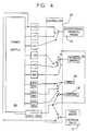
- FIG. 4is a schematic diagram showing the connection of the devices depicted in FIGS. 1 and 2 to a power supply as controlled by a controller.
- FIG. 1shows an electrophoretic display 10 in accordance with the present invention.
- the display 10has an anode faceplate 12 and a cathode faceplate 14 which are sealably affixed on either side of intermediate spacers 16a and 16b to form a fluid tight envelope for containing dielectric/pigment particle suspension or electrophoretic fluid (not shown).
- the faceplates 12 and 14are typically flat glass plates upon which are deposited conductor elements to comprise the site of electrostatic charge for inducing motion in the electrophoretic fluid.
- the techniques, materials and dimensions used to form the conductor elements upon the faceplates and the methods for making EPIDS, in general,are shown in U.S. Patent Nos. 4,655,897, 4,732,830 and 4,742,345.
- a plurality of independent, electrically conductive cathode members 18are deposited upon the cathode faceplate 14 using conventional deposition and etching techniques. It is preferred that the cathode members 18 be composed of Indium Tin Oxide (ITO) as set forth in U.S. Patent No. 4,742,345.
- ITOIndium Tin Oxide
- a plurality of independent grid conductor members 20are superimposed in the vertical over the cathode members 18 and are insulated therefrom by an interstitial photoresist layer 22 (see FIG. 2).
- the grid members 20may be formed by coating the photoresist layer 22 with a metal, such as nickel, using sputtering techniques or the like, and then selectively masking and etching to yield the intersecting but insulated configuration shown in FIGS. 1 and 2.
- a metalsuch as nickel
- the overlaying of grid lines 20 upon cathode lines 18creates a plurality of wells 21 bounded by the intersecting lines 20 and 18.
- more wells 21may be defined by forming the grid 20 and cathode 18 lines in a tyned configuration.
- the wells 21communicate with the fluid contained within the EPID and thus permit pigment particles to travel close to the glass cathode faceplate 14 where they are most clearly visible.
- An anode 26is formed on an interior surface of the anode faceplate 12 by plating with a thin layer of conductor material, such as, chrome.
- a mesh element or screen 28is sandwiched between spacers 16a and 16b to provide at least a partial barrier to the passage of light through the EPID 10.
- the mesh screen 28has a plurality of pores 29 through which pigment particles may pass so as not to obstruct the normal operation of the EPID.
- the meshitself is an optically significant element, i.e., it is readily visible to the naked eye. It is preferred that the mesh appear as a flat planar object. This is achieved by making the mesh with the minimum pore size which does not critically impede pigment movement.
- a mesh screen having suitable characteristicsis commercially available from the Buckee Mears Co., viz., a perforated stainless steel mesh having an approximate thickness and pore size of 0.254 mm to 0.305 mm (10 to 12 mils).
- the meshhas an open area ratio, i.e., the ratio of the sum of pore area to the total surface area on one surface of the screen, of approximately 40% to 50%.
- the meshis blackened by an anodizing process.
- the significance of the mesh screen 28is that it provides a solid visual background for the display of pixels and it permits a reduction of dye concentration to effect a desired background intensity. It has also been observed that the above-described mesh screen provides such an effective background that no dye is required.
- the mesh screen 28also functions to prevent inadvertent backlighting due to the overall translucence of the EPID 10. It should be observed that the screen 28 is positioned in the EPID 10 such that when the pigment is in the display position, it is on one side of the screen 28 and when it is in the written position it is on the other side of the screen 28, obscured from view by the screen 28 and/or dye in the solution.
- the screen 28is fabricated from an electrically conductive material so that it can be utilized to carry an electric charge for the purpose of aiding in controlling the movement of the pigment particles.
- FIGS 1 and 2illustrate the incorporation of the mesh screen 28 into a tetrode-type display.
- the tetrode displayincludes a plurality of local anode elements 32 which are deposited upon corresponding photoresist insulator strips 34 (see FIG. 2) formed perpendicular to the grid elements 20.
- the methods for forming the local anode elements 32are set forth at length in U.S. Patent No. 5,053,763. In brief, a layer of SiO2 is applied over the grid elements 20, followed by a layer of photoresist.
- a layer of metale.g., nickel or aluminum, is applied over the photoresist layer.
- Yet another layer of photoresistis applied over the metal layer, and is then masked, exposed and developed perpendicular to the grid elements.
- the metal layeris then etched with a suitable solution.
- the photoresistis then plasma etched down to the cathode structure.
- the partsmay be assembled in a stack and placed in an oven for baking.
- the spacers 16a and 16bin that case, would be coated on surfaces which contact adjacent elements with a material which would become plastic at baking temperatures, such as, epoxy.
- the meltable materialflows and the elements form a laminate upon cooling.
- other methodsexist within the scope of the normally skilled artisan for assembling the elements of the EPID 10 shown, such as, e.g., gluing.
- the lamination of the EPID elementsforms an envelope for containing the dielectric fluid/pigment particle suspension.
- the discrete cathode and grid members 18 and 20 of the electrophoretic display 10can assume a variety of voltages during operation for controlling the display operations of erase, hold and write at the numerous points of intersection defining a cathode/grid matrix.
- a display panelwould have a large number of intersections, e.g., 2,200 x 1,700 or a total of 3,740,000 separately addressable intersection points.
- cathode members 18 and grid members 20are depicted.
- the shape and proportions of the elements depictedare for purposes of illustration only. The dimensions of the respective elements have also been greatly enlarged for illustration and are not necessarily in proportion to an actual operational device. More illustrations of electrophoretic displays, their components and electrical circuitry can be seen by referring to U.S. Patents Nos. 4,742,345 and 4,772,820, each being awarded to the inventors herein.
- each local anode linehave a tined configuration as described more specifically below.
- FIG. 2shows the electrophoretic display of FIG. 1 assembled and in cross-section.
- the remote anode 26 in the embodiment shownis a plate-like area of conductor material having a length and width essentially matching that of the cathode/grid matrix, i.e., coextensive with the matrix, as is taught in the above referenced patents and applications of the present Applicant.
- the cathode elements 18, grid elements 20 and grid insulator strips 22as are also like those shown in the foregoing patents, etc. Since all conductor elements are quite thin, they extend beneath the interstitial spacers 16a and 16b without special provision and at least one end thereof provide a terminal exterior to the envelope for connecting display driver circuitry (not shown).
- epoxy bonding material 30is depicted providing the laminating bond between spacers 16 and the faceplates 12 and 14 and for laminating the mesh screen 28 between the spacers 16a and b.
- Each local anode line 32preferably has four tines 33 which may, for example be about 16.8um wide and separated by a space 35 approximately 15 um wide, each tine rejoining a common electrically continuous portion of the local anode at both terminal ends.
- the GRIDis raised to GRID (VDD) and the returned to GRID (VSS) to remove excess pigment from the wells.
- VDDGRID
- VSSGRID
- Pigmentmoves from the MESH to the REMOTE ANODE by applying the following voltages:
- the imageis then written on the local anode by selectively raising appropriate grid lines to GRID (VDD) and sequentially lowering cathode lines to 0 volts.
- VDDGRID
- the pigmentpasses from the cathode faceplate through the spaces between the local anode tines to the local anode.
- the purpose of writing to the local anodeis to permit subsequent erasure of the panel from the local anode which eliminates the flash which occurs when erasing from the remote anode and also to permit single character erase and rewrite.
- the local anode linesare driven individually.
- the grid, cathode and local anode lines intersecting at that pixelare given the following potentials:
- FIG. 4illustrates in schematic form how the various components of the electrophoretic display described above in reference to FIGS. 1 and 2 might be electrically connected to a suitable power supply 36 under the control of a digital controller 38 in order to assume the correct voltage states during the operations described.
Landscapes
- Physics & Mathematics (AREA)
- Nonlinear Science (AREA)
- General Physics & Mathematics (AREA)
- Optics & Photonics (AREA)
- Engineering & Computer Science (AREA)
- Computer Hardware Design (AREA)
- Theoretical Computer Science (AREA)
- Health & Medical Sciences (AREA)
- Life Sciences & Earth Sciences (AREA)
- Chemical & Material Sciences (AREA)
- Chemical Kinetics & Catalysis (AREA)
- Electrochemistry (AREA)
- Molecular Biology (AREA)
- Electrochromic Elements, Electrophoresis, Or Variable Reflection Or Absorption Elements (AREA)
- Control Of Indicators Other Than Cathode Ray Tubes (AREA)
- Devices For Indicating Variable Information By Combining Individual Elements (AREA)
Abstract
Description
- All other grids = GRID (VSS)
- All other local anodes = +V3
- All other cathodes = CATH. (VDD)
Claims (8)
- A method of operating a tetrode-type electrophoreticdisplay (10) of the type having a plurality of parallelcathode lines (18) arranged in a given direction, a plurality ofparallel grid lines (20) insulated from said cathode lines andperpendicular thereto to form an X-Y addressing matrix, a pluralityof local anode lines (32) deposited upon said grid lines perpendicularthereto and insulated therefrom by insulator strips(34), a remote anode (26) separated from said local anode lineswith space therebetween accommodating an electrophoretic dispersionincluding pigments particles suspended in a fluid and anelectrically conductive screen (28) allowing said pigment particlesto pass therethrough, characterized by the steps of:electrically connecting said cathode lines (18), saidgrid lines (20), said screen (28), said local anode lines (32)and said remote anode (26) to a source of electrical potentialenergy, said source simultaneously providing a selected set ofindependent voltages to each of said cathode lines, said gridlines, said screen, said local anode lines and said remote anodeunder the control of control means (38) for controlling saidindependent voltages supplied by said source; andselectively erasing single pixels previously written onsaid display by controlling said source of electrical potentialenergy with said control means such that voltage levels areapplied to said cathode lines (18), said grid lines (20), saidscreen (28), said local anode lines (32) and said remote anode(26), wherein said step of selectively erasing single pixelsincludes providing a voltage of approximately GRID (VDD) toselected said grid lines and a voltage of approximately 0 toselected said local anode lines intersecting said selected gridlines at said single pixels to be erased, said GRID (VDD) voltagecorresponding, during the erasing step, to a zero voltage level.
- The method of claim 1, further including a step oflocal anode writing prior to said step of selectively erasing,wherein said previously written single pixels are written uponsaid local anode (32).
- The method of claim 2, wherein said step of selectivelyerasing single pixels includes maintaining all grid lines(20) other than those intersecting pixels to be erased at anapproximate voltage of GRID (VSS); maintaining all local anodelines (32) other than those intersecting pixels to be erased atvoltage approximately +V3; and maintaining a voltage of approximatelyCATH (VDD) on said cathode lines (18).
- The method of claim 3, further including placingsaid local anode lines (32) in a hold condition by providingapproximate voltage levels of +V3 to said remote anode (26), 0volts to said screen (28), +V3 to said local anode lines, GRID(VSS) to said grid lines (20), and CATH (VDD) to said cathodelines (18) before said step of local anode writing.
- The method of claim 4, wherein said grid lines (20)and said cathode lines (18) of said X-Y matrix define a pluralityof wells (21) proximate said plurality of intersections thereof,said wells communicating with said space accommodating said fluidand further including a step of removing excess pigment from saidwells and inducing the movement of pigment from said screen (28)to said remote anode (26) by providing approximate voltage levelsof +V1 to said remote anode, VAC to said screen, 0 to said localanode lines (32), GRID (VSS) to said grid lines, and CATH (VDD)to said cathode lines prior to said step of placing said localanode lines in a hold condition.
- The method of claim 5, further including a step ofplacing said selectively erased single pixels in a hold conditionafter said step of selective pixel erasure by providing approximatevoltage levels of GRID (VSS) to said selected said gridlines (20) and +V3 to said selected said local anode lines (32)intersecting said selected said grid lines.
- The method of claim 6, further including a step offully erasing said display prior to said step of removing excesspigment by providing approximate voltage levels of -V1 to saidremote anode (26), -V2 to said screen (28), 0 to said local anode(32), GRID (VDD) to said grid lines (20) and 0 to said cathodelines (18).
- The method of claim 7, further including the step ofplacing said display in a preliminary hold condition after saidstep of fully erasing and prior to said step of removing excesspigment by providing approximate voltage levels of +V1 to saidremote anode (26), +V2 to said screen (28), 0 to said local anodelines (32), GRID (VSS) to said grid lines (20) and CATH (VDD) tosaid cathode lines (18).
Applications Claiming Priority (3)
| Application Number | Priority Date | Filing Date | Title |
|---|---|---|---|
| US07/841,380US5293528A (en) | 1992-02-25 | 1992-02-25 | Electrophoretic display panel and associated methods providing single pixel erase capability |
| PCT/US1993/000898WO1993017414A1 (en) | 1992-02-25 | 1993-01-29 | Electrophoretic display panel and associated methods providing single pixel erase capability |
| US841380 | 2001-04-24 |
Publications (3)
| Publication Number | Publication Date |
|---|---|
| EP0628194A1 EP0628194A1 (en) | 1994-12-14 |
| EP0628194A4 EP0628194A4 (en) | 1995-05-31 |
| EP0628194B1true EP0628194B1 (en) | 1998-07-22 |
Family
ID=25284723
Family Applications (1)
| Application Number | Title | Priority Date | Filing Date |
|---|---|---|---|
| EP93904812AExpired - LifetimeEP0628194B1 (en) | 1992-02-25 | 1993-01-29 | Electrophoretic display panel and associated methods providing single pixel erase capability |
Country Status (6)
| Country | Link |
|---|---|
| US (1) | US5293528A (en) |
| EP (1) | EP0628194B1 (en) |
| JP (1) | JP2825656B2 (en) |
| CA (1) | CA2130753C (en) |
| DE (1) | DE69319898T2 (en) |
| WO (1) | WO1993017414A1 (en) |
Families Citing this family (109)
| Publication number | Priority date | Publication date | Assignee | Title |
|---|---|---|---|---|
| US5745094A (en)* | 1994-12-28 | 1998-04-28 | International Business Machines Corporation | Electrophoretic display |
| US6727881B1 (en) | 1995-07-20 | 2004-04-27 | E Ink Corporation | Encapsulated electrophoretic displays and methods and materials for making the same |
| US7071913B2 (en)* | 1995-07-20 | 2006-07-04 | E Ink Corporation | Retroreflective electrophoretic displays and materials for making the same |
| US6710540B1 (en) | 1995-07-20 | 2004-03-23 | E Ink Corporation | Electrostatically-addressable electrophoretic display |
| US7304634B2 (en)* | 1995-07-20 | 2007-12-04 | E Ink Corporation | Rear electrode structures for electrophoretic displays |
| US7999787B2 (en) | 1995-07-20 | 2011-08-16 | E Ink Corporation | Methods for driving electrophoretic displays using dielectrophoretic forces |
| US7106296B1 (en) | 1995-07-20 | 2006-09-12 | E Ink Corporation | Electronic book with multiple page displays |
| US6515649B1 (en) | 1995-07-20 | 2003-02-04 | E Ink Corporation | Suspended particle displays and materials for making the same |
| US6664944B1 (en) | 1995-07-20 | 2003-12-16 | E-Ink Corporation | Rear electrode structures for electrophoretic displays |
| US7583251B2 (en)* | 1995-07-20 | 2009-09-01 | E Ink Corporation | Dielectrophoretic displays |
| US7193625B2 (en)* | 1999-04-30 | 2007-03-20 | E Ink Corporation | Methods for driving electro-optic displays, and apparatus for use therein |
| US7352353B2 (en)* | 1995-07-20 | 2008-04-01 | E Ink Corporation | Electrostatically addressable electrophoretic display |
| US7167155B1 (en) | 1995-07-20 | 2007-01-23 | E Ink Corporation | Color electrophoretic displays |
| US7109968B2 (en)* | 1995-07-20 | 2006-09-19 | E Ink Corporation | Non-spherical cavity electrophoretic displays and methods and materials for making the same |
| US8139050B2 (en)* | 1995-07-20 | 2012-03-20 | E Ink Corporation | Addressing schemes for electronic displays |
| US6124851A (en) | 1995-07-20 | 2000-09-26 | E Ink Corporation | Electronic book with multiple page displays |
| US6120839A (en) | 1995-07-20 | 2000-09-19 | E Ink Corporation | Electro-osmotic displays and materials for making the same |
| US6262706B1 (en) | 1995-07-20 | 2001-07-17 | E Ink Corporation | Retroreflective electrophoretic displays and materials for making the same |
| US6232950B1 (en) | 1997-08-28 | 2001-05-15 | E Ink Corporation | Rear electrode structures for displays |
| US7242513B2 (en)* | 1997-08-28 | 2007-07-10 | E Ink Corporation | Encapsulated electrophoretic displays having a monolayer of capsules and materials and methods for making the same |
| US6839158B2 (en) | 1997-08-28 | 2005-01-04 | E Ink Corporation | Encapsulated electrophoretic displays having a monolayer of capsules and materials and methods for making the same |
| US7247379B2 (en)* | 1997-08-28 | 2007-07-24 | E Ink Corporation | Electrophoretic particles, and processes for the production thereof |
| US6300932B1 (en) | 1997-08-28 | 2001-10-09 | E Ink Corporation | Electrophoretic displays with luminescent particles and materials for making the same |
| US6067185A (en) | 1997-08-28 | 2000-05-23 | E Ink Corporation | Process for creating an encapsulated electrophoretic display |
| US6825829B1 (en)* | 1997-08-28 | 2004-11-30 | E Ink Corporation | Adhesive backed displays |
| US6177921B1 (en) | 1997-08-28 | 2001-01-23 | E Ink Corporation | Printable electrode structures for displays |
| US7002728B2 (en)* | 1997-08-28 | 2006-02-21 | E Ink Corporation | Electrophoretic particles, and processes for the production thereof |
| US6704133B2 (en) | 1998-03-18 | 2004-03-09 | E-Ink Corporation | Electro-optic display overlays and systems for addressing such displays |
| US6445489B1 (en) | 1998-03-18 | 2002-09-03 | E Ink Corporation | Electrophoretic displays and systems for addressing such displays |
| US6518949B2 (en) | 1998-04-10 | 2003-02-11 | E Ink Corporation | Electronic displays using organic-based field effect transistors |
| US7075502B1 (en) | 1998-04-10 | 2006-07-11 | E Ink Corporation | Full color reflective display with multichromatic sub-pixels |
| WO1999059101A2 (en) | 1998-05-12 | 1999-11-18 | E-Ink Corporation | Microencapsulated electrophoretic electrostatically-addressed media for drawing device applications |
| DE69920228T2 (en)* | 1998-07-08 | 2005-01-27 | E-Ink Corp., Cambridge | METHOD FOR IMPROVING COLOR REPRODUCTION IN ELECTROPHORETIC DEVICES USING MICROCAPSULES |
| USD485294S1 (en) | 1998-07-22 | 2004-01-13 | E Ink Corporation | Electrode structure for an electronic display |
| US7256766B2 (en) | 1998-08-27 | 2007-08-14 | E Ink Corporation | Electrophoretic display comprising optical biasing element |
| US6225971B1 (en) | 1998-09-16 | 2001-05-01 | International Business Machines Corporation | Reflective electrophoretic display with laterally adjacent color cells using an absorbing panel |
| US6184856B1 (en) | 1998-09-16 | 2001-02-06 | International Business Machines Corporation | Transmissive electrophoretic display with laterally adjacent color cells |
| US6271823B1 (en) | 1998-09-16 | 2001-08-07 | International Business Machines Corporation | Reflective electrophoretic display with laterally adjacent color cells using a reflective panel |
| US6144361A (en)* | 1998-09-16 | 2000-11-07 | International Business Machines Corporation | Transmissive electrophoretic display with vertical electrodes |
| EP1118039B1 (en) | 1998-10-07 | 2003-02-05 | E Ink Corporation | Illumination system for nonemissive electronic displays |
| AU6293499A (en) | 1998-10-07 | 2000-04-26 | E-Ink Corporation | Capsules for electrophoretic displays and methods for making the same |
| US6312304B1 (en) | 1998-12-15 | 2001-11-06 | E Ink Corporation | Assembly of microencapsulated electronic displays |
| US6724519B1 (en) | 1998-12-21 | 2004-04-20 | E-Ink Corporation | Protective electrodes for electrophoretic displays |
| EP1169121B1 (en) | 1999-04-06 | 2012-10-31 | E Ink Corporation | Methods for producing droplets for use in capsule-based electrophoretic displays |
| US6498114B1 (en) | 1999-04-09 | 2002-12-24 | E Ink Corporation | Method for forming a patterned semiconductor film |
| US6842657B1 (en) | 1999-04-09 | 2005-01-11 | E Ink Corporation | Reactive formation of dielectric layers and protection of organic layers in organic semiconductor device fabrication |
| US6504524B1 (en) | 2000-03-08 | 2003-01-07 | E Ink Corporation | Addressing methods for displays having zero time-average field |
| US7119772B2 (en)* | 1999-04-30 | 2006-10-10 | E Ink Corporation | Methods for driving bistable electro-optic displays, and apparatus for use therein |
| US6531997B1 (en) | 1999-04-30 | 2003-03-11 | E Ink Corporation | Methods for addressing electrophoretic displays |
| US7012600B2 (en)* | 1999-04-30 | 2006-03-14 | E Ink Corporation | Methods for driving bistable electro-optic displays, and apparatus for use therein |
| US7038655B2 (en) | 1999-05-03 | 2006-05-02 | E Ink Corporation | Electrophoretic ink composed of particles with field dependent mobilities |
| US8115729B2 (en) | 1999-05-03 | 2012-02-14 | E Ink Corporation | Electrophoretic display element with filler particles |
| US6693620B1 (en) | 1999-05-03 | 2004-02-17 | E Ink Corporation | Threshold addressing of electrophoretic displays |
| US7030412B1 (en) | 1999-05-05 | 2006-04-18 | E Ink Corporation | Minimally-patterned semiconductor devices for display applications |
| AU5779200A (en) | 1999-07-01 | 2001-01-22 | E-Ink Corporation | Electrophoretic medium provided with spacers |
| EP1196814A1 (en)* | 1999-07-21 | 2002-04-17 | E Ink Corporation | Use of a storage capacitor to enhance the performance of an active matrix driven electronic display |
| CN1237623C (en) | 2000-04-18 | 2006-01-18 | 伊英克公司 | Method for forming transistor on substrate and substrate containing polyphenylene polyimide |
| US7893435B2 (en)* | 2000-04-18 | 2011-02-22 | E Ink Corporation | Flexible electronic circuits and displays including a backplane comprising a patterned metal foil having a plurality of apertures extending therethrough |
| US6683333B2 (en) | 2000-07-14 | 2004-01-27 | E Ink Corporation | Fabrication of electronic circuit elements using unpatterned semiconductor layers |
| US7236290B1 (en) | 2000-07-25 | 2007-06-26 | E Ink Corporation | Electrophoretic medium with improved stability |
| US6816147B2 (en)* | 2000-08-17 | 2004-11-09 | E Ink Corporation | Bistable electro-optic display, and method for addressing same |
| JP2004522179A (en)* | 2000-11-29 | 2004-07-22 | イー−インク コーポレイション | Addressing scheme for electronic displays |
| US7230750B2 (en) | 2001-05-15 | 2007-06-12 | E Ink Corporation | Electrophoretic media and processes for the production thereof |
| US20050156340A1 (en)* | 2004-01-20 | 2005-07-21 | E Ink Corporation | Preparation of capsules |
| US20100148385A1 (en)* | 2001-05-15 | 2010-06-17 | E Ink Corporation | Electrophoretic media and processes for the production thereof |
| US6982178B2 (en)* | 2002-06-10 | 2006-01-03 | E Ink Corporation | Components and methods for use in electro-optic displays |
| US6967640B2 (en)* | 2001-07-27 | 2005-11-22 | E Ink Corporation | Microencapsulated electrophoretic display with integrated driver |
| US8593396B2 (en) | 2001-11-20 | 2013-11-26 | E Ink Corporation | Methods and apparatus for driving electro-optic displays |
| US9412314B2 (en) | 2001-11-20 | 2016-08-09 | E Ink Corporation | Methods for driving electro-optic displays |
| US9530363B2 (en) | 2001-11-20 | 2016-12-27 | E Ink Corporation | Methods and apparatus for driving electro-optic displays |
| US8558783B2 (en)* | 2001-11-20 | 2013-10-15 | E Ink Corporation | Electro-optic displays with reduced remnant voltage |
| US7528822B2 (en)* | 2001-11-20 | 2009-05-05 | E Ink Corporation | Methods for driving electro-optic displays |
| US7952557B2 (en)* | 2001-11-20 | 2011-05-31 | E Ink Corporation | Methods and apparatus for driving electro-optic displays |
| US8125501B2 (en) | 2001-11-20 | 2012-02-28 | E Ink Corporation | Voltage modulated driver circuits for electro-optic displays |
| US6865010B2 (en)* | 2001-12-13 | 2005-03-08 | E Ink Corporation | Electrophoretic electronic displays with low-index films |
| US6900851B2 (en) | 2002-02-08 | 2005-05-31 | E Ink Corporation | Electro-optic displays and optical systems for addressing such displays |
| US7583427B2 (en)* | 2002-06-10 | 2009-09-01 | E Ink Corporation | Components and methods for use in electro-optic displays |
| US8049947B2 (en)* | 2002-06-10 | 2011-11-01 | E Ink Corporation | Components and methods for use in electro-optic displays |
| US7843621B2 (en)* | 2002-06-10 | 2010-11-30 | E Ink Corporation | Components and testing methods for use in the production of electro-optic displays |
| US9470950B2 (en) | 2002-06-10 | 2016-10-18 | E Ink Corporation | Electro-optic displays, and processes for the production thereof |
| US7110164B2 (en)* | 2002-06-10 | 2006-09-19 | E Ink Corporation | Electro-optic displays, and processes for the production thereof |
| US8363299B2 (en)* | 2002-06-10 | 2013-01-29 | E Ink Corporation | Electro-optic displays, and processes for the production thereof |
| US20110199671A1 (en)* | 2002-06-13 | 2011-08-18 | E Ink Corporation | Methods for driving electrophoretic displays using dielectrophoretic forces |
| US20080024482A1 (en)* | 2002-06-13 | 2008-01-31 | E Ink Corporation | Methods for driving electro-optic displays |
| US7312916B2 (en)* | 2002-08-07 | 2007-12-25 | E Ink Corporation | Electrophoretic media containing specularly reflective particles |
| EP3056941B1 (en) | 2002-09-03 | 2019-01-09 | E Ink Corporation | Electro-phoretic medium |
| US7839564B2 (en)* | 2002-09-03 | 2010-11-23 | E Ink Corporation | Components and methods for use in electro-optic displays |
| US20130063333A1 (en) | 2002-10-16 | 2013-03-14 | E Ink Corporation | Electrophoretic displays |
| US10726798B2 (en) | 2003-03-31 | 2020-07-28 | E Ink Corporation | Methods for operating electro-optic displays |
| US8174490B2 (en)* | 2003-06-30 | 2012-05-08 | E Ink Corporation | Methods for driving electrophoretic displays |
| WO2005010598A2 (en) | 2003-07-24 | 2005-02-03 | E Ink Corporation | Electro-optic displays |
| EP1656658A4 (en)* | 2003-08-19 | 2009-12-30 | E Ink Corp | Methods for controlling electro-optic displays |
| US8928562B2 (en) | 2003-11-25 | 2015-01-06 | E Ink Corporation | Electro-optic displays, and methods for driving same |
| US7492339B2 (en)* | 2004-03-26 | 2009-02-17 | E Ink Corporation | Methods for driving bistable electro-optic displays |
| US11250794B2 (en) | 2004-07-27 | 2022-02-15 | E Ink Corporation | Methods for driving electrophoretic displays using dielectrophoretic forces |
| US7453445B2 (en) | 2004-08-13 | 2008-11-18 | E Ink Corproation | Methods for driving electro-optic displays |
| US20080043318A1 (en)* | 2005-10-18 | 2008-02-21 | E Ink Corporation | Color electro-optic displays, and processes for the production thereof |
| US7746541B2 (en)* | 2006-03-13 | 2010-06-29 | Honeywell International Inc. | System and apparatus for an electrophoretic display |
| US7685967B2 (en) | 2006-05-23 | 2010-03-30 | Seed Resources, Llc | Feed cake assembly |
| US7307779B1 (en) | 2006-09-21 | 2007-12-11 | Honeywell International, Inc. | Transmissive E-paper display |
| US8623191B2 (en)* | 2006-09-22 | 2014-01-07 | Honeywell International Inc. | Non-volatile addressable electronic paper with gray level capability |
| US7675672B2 (en)* | 2006-11-09 | 2010-03-09 | Honeywell International Inc. | Non-volatile addressable electronic paper for disposable flexible displays |
| US7843623B2 (en)* | 2006-11-16 | 2010-11-30 | Honeywell International Inc. | Non volatile addressable electronic paper with color capability |
| JP5381671B2 (en)* | 2009-12-11 | 2014-01-08 | 富士ゼロックス株式会社 | Display device |
| US7957054B1 (en) | 2009-12-21 | 2011-06-07 | Hewlett-Packard Development Company, L.P. | Electro-optical display systems |
| US8089687B2 (en)* | 2009-12-21 | 2012-01-03 | Hewlett-Packard Development Company, L.P. | Electro-optical display systems |
| TWI591604B (en) | 2010-04-09 | 2017-07-11 | 電子墨水股份有限公司 | Methods for driving electro-optic displays |
| CN103677726B (en)* | 2012-09-02 | 2017-03-01 | 元太科技工业股份有限公司 | Double-screen electronic device and detachable display module thereof |
| CN112180628A (en)* | 2020-09-11 | 2021-01-05 | 山东蓝贝思特教装集团股份有限公司 | Liquid crystal writing device, local erasing method and display method |
Family Cites Families (4)
| Publication number | Priority date | Publication date | Assignee | Title |
|---|---|---|---|---|
| US5041824A (en)* | 1989-03-02 | 1991-08-20 | Copytele, Inc. | Semitransparent electrophoretic information displays (EPID) employing mesh like electrodes |
| US5053763A (en)* | 1989-05-01 | 1991-10-01 | Copytele, Inc. | Dual anode flat panel electrophoretic display apparatus |
| US5177476A (en)* | 1989-11-24 | 1993-01-05 | Copytele, Inc. | Methods of fabricating dual anode, flat panel electrophoretic displays |
| US5077157A (en)* | 1989-11-24 | 1991-12-31 | Copytele, Inc. | Methods of fabricating dual anode, flat panel electrophoretic displays |
- 1992
- 1992-02-25USUS07/841,380patent/US5293528A/ennot_activeExpired - Fee Related
- 1993
- 1993-01-29CACA002130753Apatent/CA2130753C/ennot_activeExpired - Fee Related
- 1993-01-29EPEP93904812Apatent/EP0628194B1/ennot_activeExpired - Lifetime
- 1993-01-29JPJP5514870Apatent/JP2825656B2/ennot_activeExpired - Lifetime
- 1993-01-29WOPCT/US1993/000898patent/WO1993017414A1/enactiveIP Right Grant
- 1993-01-29DEDE69319898Tpatent/DE69319898T2/ennot_activeExpired - Fee Related
Also Published As
| Publication number | Publication date |
|---|---|
| JP2825656B2 (en) | 1998-11-18 |
| JPH07504048A (en) | 1995-04-27 |
| WO1993017414A1 (en) | 1993-09-02 |
| CA2130753C (en) | 1998-07-21 |
| EP0628194A1 (en) | 1994-12-14 |
| DE69319898T2 (en) | 1999-03-18 |
| CA2130753A1 (en) | 1993-08-26 |
| EP0628194A4 (en) | 1995-05-31 |
| DE69319898D1 (en) | 1998-08-27 |
| US5293528A (en) | 1994-03-08 |
Similar Documents
| Publication | Publication Date | Title |
|---|---|---|
| EP0628194B1 (en) | Electrophoretic display panel and associated methods providing single pixel erase capability | |
| EP0632919B1 (en) | Electrophoretic display panel for blinking displayed characters | |
| US5412398A (en) | Electrophoretic display panel and associated methods for blinking displayed characters | |
| EP0600878B1 (en) | Electrophoretic display panel with internal mesh background screen | |
| EP0601075B1 (en) | Electrophoretic display with single character erasure | |
| US5304439A (en) | Method of making an electrophoretic display panel with interleaved local anode | |
| EP0679284B1 (en) | Electrophoretic display panel with interleaved cathode and anode | |
| EP0396247B1 (en) | Dual anode flat panel electrophoretic display apparatus | |
| WO1995010107A1 (en) | Electrophoretic display panel with selective character addressability | |
| WO1993000672A1 (en) | Dual anode flat panel electrophoretic display apparatus |
Legal Events
| Date | Code | Title | Description |
|---|---|---|---|
| PUAI | Public reference made under article 153(3) epc to a published international application that has entered the european phase | Free format text:ORIGINAL CODE: 0009012 | |
| 17P | Request for examination filed | Effective date:19940920 | |
| AK | Designated contracting states | Kind code of ref document:A1 Designated state(s):BE DE FR GB IT NL | |
| A4 | Supplementary search report drawn up and despatched | Effective date:19950411 | |
| AK | Designated contracting states | Kind code of ref document:A4 Designated state(s):BE DE FR GB IT NL | |
| 17Q | First examination report despatched | Effective date:19960806 | |
| GRAG | Despatch of communication of intention to grant | Free format text:ORIGINAL CODE: EPIDOS AGRA | |
| GRAG | Despatch of communication of intention to grant | Free format text:ORIGINAL CODE: EPIDOS AGRA | |
| GRAH | Despatch of communication of intention to grant a patent | Free format text:ORIGINAL CODE: EPIDOS IGRA | |
| GRAH | Despatch of communication of intention to grant a patent | Free format text:ORIGINAL CODE: EPIDOS IGRA | |
| GRAA | (expected) grant | Free format text:ORIGINAL CODE: 0009210 | |
| AK | Designated contracting states | Kind code of ref document:B1 Designated state(s):BE DE FR GB IT NL | |
| REF | Corresponds to: | Ref document number:69319898 Country of ref document:DE Date of ref document:19980827 | |
| ET | Fr: translation filed | ||
| PLBE | No opposition filed within time limit | Free format text:ORIGINAL CODE: 0009261 | |
| STAA | Information on the status of an ep patent application or granted ep patent | Free format text:STATUS: NO OPPOSITION FILED WITHIN TIME LIMIT | |
| 26N | No opposition filed | ||
| PGFP | Annual fee paid to national office [announced via postgrant information from national office to epo] | Ref country code:FR Payment date:20010112 Year of fee payment:9 | |
| PGFP | Annual fee paid to national office [announced via postgrant information from national office to epo] | Ref country code:BE Payment date:20010119 Year of fee payment:9 | |
| PGFP | Annual fee paid to national office [announced via postgrant information from national office to epo] | Ref country code:DE Payment date:20010124 Year of fee payment:9 | |
| PGFP | Annual fee paid to national office [announced via postgrant information from national office to epo] | Ref country code:GB Payment date:20010125 Year of fee payment:9 | |
| PGFP | Annual fee paid to national office [announced via postgrant information from national office to epo] | Ref country code:NL Payment date:20010131 Year of fee payment:9 | |
| REG | Reference to a national code | Ref country code:GB Ref legal event code:IF02 | |
| PG25 | Lapsed in a contracting state [announced via postgrant information from national office to epo] | Ref country code:GB Free format text:LAPSE BECAUSE OF NON-PAYMENT OF DUE FEES Effective date:20020129 | |
| PG25 | Lapsed in a contracting state [announced via postgrant information from national office to epo] | Ref country code:BE Free format text:LAPSE BECAUSE OF NON-PAYMENT OF DUE FEES Effective date:20020131 | |
| BERE | Be: lapsed | Owner name:COPYTELE INC. Effective date:20020131 | |
| PG25 | Lapsed in a contracting state [announced via postgrant information from national office to epo] | Ref country code:NL Free format text:LAPSE BECAUSE OF NON-PAYMENT OF DUE FEES Effective date:20020801 Ref country code:DE Free format text:LAPSE BECAUSE OF NON-PAYMENT OF DUE FEES Effective date:20020801 | |
| GBPC | Gb: european patent ceased through non-payment of renewal fee | Effective date:20020129 | |
| PG25 | Lapsed in a contracting state [announced via postgrant information from national office to epo] | Ref country code:FR Free format text:LAPSE BECAUSE OF NON-PAYMENT OF DUE FEES Effective date:20020930 | |
| NLV4 | Nl: lapsed or anulled due to non-payment of the annual fee | Effective date:20020801 | |
| REG | Reference to a national code | Ref country code:FR Ref legal event code:ST | |
| PG25 | Lapsed in a contracting state [announced via postgrant information from national office to epo] | Ref country code:IT Free format text:LAPSE BECAUSE OF NON-PAYMENT OF DUE FEES;WARNING: LAPSES OF ITALIAN PATENTS WITH EFFECTIVE DATE BEFORE 2007 MAY HAVE OCCURRED AT ANY TIME BEFORE 2007. THE CORRECT EFFECTIVE DATE MAY BE DIFFERENT FROM THE ONE RECORDED. Effective date:20050129 |