EP0610587B1 - Digital signal processing apparatus - Google Patents
Digital signal processing apparatusDownload PDFInfo
- Publication number
- EP0610587B1 EP0610587B1EP93120441AEP93120441AEP0610587B1EP 0610587 B1EP0610587 B1EP 0610587B1EP 93120441 AEP93120441 AEP 93120441AEP 93120441 AEP93120441 AEP 93120441AEP 0610587 B1EP0610587 B1EP 0610587B1
- Authority
- EP
- European Patent Office
- Prior art keywords
- fade
- signal
- frequency components
- digital
- component
- Prior art date
- Legal status (The legal status is an assumption and is not a legal conclusion. Google has not performed a legal analysis and makes no representation as to the accuracy of the status listed.)
- Expired - Lifetime
Links
- 238000012545processingMethods0.000titleclaimsdescription28
- 230000000694effectsEffects0.000claimsdescription26
- 238000000034methodMethods0.000claimsdescription24
- 230000008569processEffects0.000claimsdescription15
- 238000009432framingMethods0.000claimsdescription14
- 230000004044responseEffects0.000claimsdescription7
- 230000007423decreaseEffects0.000claims1
- 238000010586diagramMethods0.000description11
- 238000013139quantizationMethods0.000description11
- 230000003139buffering effectEffects0.000description10
- 230000015654memoryEffects0.000description10
- 239000000872bufferSubstances0.000description9
- 239000002131composite materialSubstances0.000description8
- 230000005236sound signalEffects0.000description8
- 230000033458reproductionEffects0.000description7
- 238000013459approachMethods0.000description4
- 230000005540biological transmissionEffects0.000description4
- 230000003247decreasing effectEffects0.000description4
- 230000009466transformationEffects0.000description4
- 230000008859changeEffects0.000description3
- 238000012937correctionMethods0.000description3
- 230000006870functionEffects0.000description2
- 230000007246mechanismEffects0.000description2
- NJPPVKZQTLUDBO-UHFFFAOYSA-NnovaluronChemical compoundC1=C(Cl)C(OC(F)(F)C(OC(F)(F)F)F)=CC=C1NC(=O)NC(=O)C1=C(F)C=CC=C1FNJPPVKZQTLUDBO-UHFFFAOYSA-N0.000description2
- 238000012856packingMethods0.000description2
- 230000008054signal transmissionEffects0.000description2
- 239000003990capacitorSubstances0.000description1
- 238000006243chemical reactionMethods0.000description1
- 230000000295complement effectEffects0.000description1
- 238000013144data compressionMethods0.000description1
- 238000013500data storageMethods0.000description1
- 230000007547defectEffects0.000description1
- 238000013461designMethods0.000description1
- 238000001514detection methodMethods0.000description1
- 239000000284extractSubstances0.000description1
- 230000007257malfunctionEffects0.000description1
- 238000004519manufacturing processMethods0.000description1
- 230000004048modificationEffects0.000description1
- 238000012986modificationMethods0.000description1
- 230000002265preventionEffects0.000description1
Images


Classifications
- H—ELECTRICITY
- H04—ELECTRIC COMMUNICATION TECHNIQUE
- H04N—PICTORIAL COMMUNICATION, e.g. TELEVISION
- H04N5/00—Details of television systems
- H04N5/222—Studio circuitry; Studio devices; Studio equipment
- H04N5/262—Studio circuits, e.g. for mixing, switching-over, change of character of image, other special effects ; Cameras specially adapted for the electronic generation of special effects
- H04N5/265—Mixing
- H—ELECTRICITY
- H04—ELECTRIC COMMUNICATION TECHNIQUE
- H04N—PICTORIAL COMMUNICATION, e.g. TELEVISION
- H04N19/00—Methods or arrangements for coding, decoding, compressing or decompressing digital video signals
- H04N19/10—Methods or arrangements for coding, decoding, compressing or decompressing digital video signals using adaptive coding
- H04N19/134—Methods or arrangements for coding, decoding, compressing or decompressing digital video signals using adaptive coding characterised by the element, parameter or criterion affecting or controlling the adaptive coding
- H04N19/142—Detection of scene cut or scene change
- H—ELECTRICITY
- H04—ELECTRIC COMMUNICATION TECHNIQUE
- H04N—PICTORIAL COMMUNICATION, e.g. TELEVISION
- H04N19/00—Methods or arrangements for coding, decoding, compressing or decompressing digital video signals
- H04N19/10—Methods or arrangements for coding, decoding, compressing or decompressing digital video signals using adaptive coding
- H04N19/169—Methods or arrangements for coding, decoding, compressing or decompressing digital video signals using adaptive coding characterised by the coding unit, i.e. the structural portion or semantic portion of the video signal being the object or the subject of the adaptive coding
- H04N19/179—Methods or arrangements for coding, decoding, compressing or decompressing digital video signals using adaptive coding characterised by the coding unit, i.e. the structural portion or semantic portion of the video signal being the object or the subject of the adaptive coding the unit being a scene or a shot
- H—ELECTRICITY
- H04—ELECTRIC COMMUNICATION TECHNIQUE
- H04N—PICTORIAL COMMUNICATION, e.g. TELEVISION
- H04N19/00—Methods or arrangements for coding, decoding, compressing or decompressing digital video signals
- H04N19/48—Methods or arrangements for coding, decoding, compressing or decompressing digital video signals using compressed domain processing techniques other than decoding, e.g. modification of transform coefficients, variable length coding [VLC] data or run-length data
- H—ELECTRICITY
- H04—ELECTRIC COMMUNICATION TECHNIQUE
- H04N—PICTORIAL COMMUNICATION, e.g. TELEVISION
- H04N19/00—Methods or arrangements for coding, decoding, compressing or decompressing digital video signals
- H04N19/85—Methods or arrangements for coding, decoding, compressing or decompressing digital video signals using pre-processing or post-processing specially adapted for video compression
- H04N19/87—Methods or arrangements for coding, decoding, compressing or decompressing digital video signals using pre-processing or post-processing specially adapted for video compression involving scene cut or scene change detection in combination with video compression
- H—ELECTRICITY
- H04—ELECTRIC COMMUNICATION TECHNIQUE
- H04N—PICTORIAL COMMUNICATION, e.g. TELEVISION
- H04N19/00—Methods or arrangements for coding, decoding, compressing or decompressing digital video signals
- H04N19/85—Methods or arrangements for coding, decoding, compressing or decompressing digital video signals using pre-processing or post-processing specially adapted for video compression
- H04N19/89—Methods or arrangements for coding, decoding, compressing or decompressing digital video signals using pre-processing or post-processing specially adapted for video compression involving methods or arrangements for detection of transmission errors at the decoder
- H04N19/895—Methods or arrangements for coding, decoding, compressing or decompressing digital video signals using pre-processing or post-processing specially adapted for video compression involving methods or arrangements for detection of transmission errors at the decoder in combination with error concealment
- H—ELECTRICITY
- H04—ELECTRIC COMMUNICATION TECHNIQUE
- H04N—PICTORIAL COMMUNICATION, e.g. TELEVISION
- H04N19/00—Methods or arrangements for coding, decoding, compressing or decompressing digital video signals
- H04N19/90—Methods or arrangements for coding, decoding, compressing or decompressing digital video signals using coding techniques not provided for in groups H04N19/10-H04N19/85, e.g. fractals
- H—ELECTRICITY
- H04—ELECTRIC COMMUNICATION TECHNIQUE
- H04N—PICTORIAL COMMUNICATION, e.g. TELEVISION
- H04N21/00—Selective content distribution, e.g. interactive television or video on demand [VOD]
- H04N21/40—Client devices specifically adapted for the reception of or interaction with content, e.g. set-top-box [STB]; Operations thereof
- H04N21/43—Processing of content or additional data, e.g. demultiplexing additional data from a digital video stream; Elementary client operations, e.g. monitoring of home network or synchronising decoder's clock; Client middleware
- H04N21/431—Generation of visual interfaces for content selection or interaction; Content or additional data rendering
- H04N21/4318—Generation of visual interfaces for content selection or interaction; Content or additional data rendering by altering the content in the rendering process, e.g. blanking, blurring or masking an image region
- H—ELECTRICITY
- H04—ELECTRIC COMMUNICATION TECHNIQUE
- H04N—PICTORIAL COMMUNICATION, e.g. TELEVISION
- H04N21/00—Selective content distribution, e.g. interactive television or video on demand [VOD]
- H04N21/40—Client devices specifically adapted for the reception of or interaction with content, e.g. set-top-box [STB]; Operations thereof
- H04N21/43—Processing of content or additional data, e.g. demultiplexing additional data from a digital video stream; Elementary client operations, e.g. monitoring of home network or synchronising decoder's clock; Client middleware
- H04N21/44—Processing of video elementary streams, e.g. splicing a video clip retrieved from local storage with an incoming video stream or rendering scenes according to encoded video stream scene graphs
- H04N21/4405—Processing of video elementary streams, e.g. splicing a video clip retrieved from local storage with an incoming video stream or rendering scenes according to encoded video stream scene graphs involving video stream decryption
- H04N21/44055—Processing of video elementary streams, e.g. splicing a video clip retrieved from local storage with an incoming video stream or rendering scenes according to encoded video stream scene graphs involving video stream decryption by partially decrypting, e.g. decrypting a video stream that has been partially encrypted
- H—ELECTRICITY
- H04—ELECTRIC COMMUNICATION TECHNIQUE
- H04N—PICTORIAL COMMUNICATION, e.g. TELEVISION
- H04N7/00—Television systems
- H04N7/16—Analogue secrecy systems; Analogue subscription systems
- H04N7/167—Systems rendering the television signal unintelligible and subsequently intelligible
- H04N7/1675—Providing digital key or authorisation information for generation or regeneration of the scrambling sequence
- H—ELECTRICITY
- H04—ELECTRIC COMMUNICATION TECHNIQUE
- H04N—PICTORIAL COMMUNICATION, e.g. TELEVISION
- H04N7/00—Television systems
- H04N7/24—Systems for the transmission of television signals using pulse code modulation
- H04N7/52—Systems for transmission of a pulse code modulated video signal with one or more other pulse code modulated signals, e.g. an audio signal or a synchronizing signal
- H04N7/54—Systems for transmission of a pulse code modulated video signal with one or more other pulse code modulated signals, e.g. an audio signal or a synchronizing signal the signals being synchronous
Definitions
- the present inventionrelates to a digital signal processing apparatus, and more particularly, to apparatus for processing compressed frequency components of a digital image signal to provide fade-in and fade-out effects and further, to provide scrambling and descrambling of the digital image signal.
- Audio-video equipmentsuch as a consumer VTR (video tape recorder) having a built-in camera (i.e. a camcorder), permit fade-in or fade-out of a video image during a scene change or the like.
- VTRvideo tape recorder
- a built-in camerai.e. a camcorder
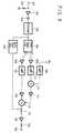
- FIG. 9illustrates one example of an arrangement of a conventional fade-in and fade-out circuit.
- a composite video signalis supplied to an input terminal 101. Since it is common that the composite video signal be transmitted at 75 ohms and 1Vp-p (peak to peak), the composite video signal is terminated by a terminating resistor 102 of 75 ohms and received by a buffer 103.
- An output from the buffer 103is supplied through a capacitor 104 to a clamper 105.
- the clamper 105is adapted to prevent a DC component of the pedestal level of the video signal from becoming unstable.
- the output of clamper 105is supplied to a Y/C separating circuit 106 and a synchronizing separating circuit 107.
- the synchronizing separating circuit 107extracts from the composite video signal a composite sync. signal from which a horizontal (H) sync. signal and a vertical (V) sync. signal are synthesized.
- the Y/C separating circuit 106separates the composite video signal to provide a luminance signal Y and a chrominance signal C which are supplied to buffers 108, 109, respectively.
- variable resistors 111 and 112pass, or attenuate, the luminance signal Y and the chrominance sign C, respectively, thereby adjusting the levels of these signals.
- Another variable resistor 110connects a power source voltage Vcc to a mixer 113, thus applying a DC voltage to the mixer. This voltage is referred to as a set-up voltage.
- variable resistor 110Normally, during a non-fade in or fade-out operation, the resistance value of variable resistor 110 is set to its maximum value and the resistance values of variable resistors 111, 112 are set to zero (short circuit) such that luminance signal Y passes through variable resistor 111, mixer 113 and buffer 114 and chrominance sign C passes through variable resistor 112 and buffer 115, whereby the original composite video signal is re-synthesized by mixer 116 and the output thereof is supplied to a buffer 118 through a switch 117.
- switch 117supplies the output of synchronizing separating circuit 107 to buffer 118.
- the output of buffer 118is supplied to output terminal 120 through an impedance matching resistor 119.
- variable resistors 111, 112are progressively increased in response to a white fade-out command and simultaneously, the resistance value of variable resistor 110 is progressively decreased.
- luminance signal Y supplied to buffer 114is held at the white level.
- a white fade-in operationis carried out by merely performing the reverse of the above described fade-out operation.
- a black fade-out operationis performed when the resistance value of variable resistor 110 is set to its maximum value for the entire aforesaid fade-out operation.
- the black fade-in operationis the reverse operation of the black fade-out operation.
- Satellite broadcasting companies and cable television companies which transmit scrambled video and audio signals via satellite or cablehave long been commercially available.
- Television viewerscannot watch or listen to broadcast video and audio signals unless the broadcast signals are de-scrambled.
- television viewerscannot enjoy picture and sound of such broadcasting unless a descrambler, leased by the broadcaster to the television viewer, descrambles the signal prior to its receipt by the television receiver.
- a descramblerleased by the broadcaster to the television viewer, descrambles the signal prior to its receipt by the television receiver.
- video and audio signalsare scrambled in such a fashion that the picture and sound are completely unrecognizable by the user, there is the risk that the user misunderstands this condition to be a malfunction of the TV receiver.
- FIG. 10shows an arrangement of a descrambler used in an existing cable TV box.
- An input terminal 41 in FIG. 10receives signals supplied from a line which is normally supplied by a cable distributer to the viewer.
- the signal supplied to input terminal 41is a scrambled RF (radio frequency) signal which is received by a tuner 43.
- An operation key 47 or a remote controller 42are utilized to select the baseband signal which is to be supplied as an output by tuner 43.
- This baseband signalis supplied to a descrambler circuit 44 which descrambles the baseband signal.
- the descrambled signalis modulated onto a predetermined broadcast frequency, such as channel 3, by a modulating circuit 45 and then output from the cable box.
- This output signalis supplied to a tuner 46 contained within a TV receiver or VTR and tuned to the predetermined broadcast frequency to reproduce the video image and audio signal.
- FIG. 11shows an arrangement of a descrambler utilized with the existing satellite broadcast systems.
- an RF signal from a BS/CS antenna 51is supplied to a BS/CS tuner 52 provided within a VTR or TV.
- Channel selectionis carried out by utilizing an operation key 58 or a remote controller 57.
- a detected output signal 53 from tuner 52is supplied to a descrambler 54.
- a video signal 55 and an audio signal 56 thus descrambled by the descrambler 54are each output twice, for example.
- One set of video and audio signals 55, 56are supplied to the line input of the VTR, and the other set of video and audio signals 55, 56 are supplied to the line input of the TV receiver.
- Descramblingis carried out by using an ID (identification) number assigned to the cable box (descrambler apparatus) and a key code contained in a corresponding broadcast signal.
- IDidentification
- the broadcasting enterprisetransmits the key code recognized by the cable box to descramble the broadcast signal.
- the key code and the ID numberare related by enciphering.
- audio-video equipmentsuch as a digital broadcasting system or a teleconference system in which a video signal is digitized and transmitted via radio waves or cable and a digital VTR records the digital signal on a magnetic tape.
- a video signalis digitized, the amount of information representing the video image is quite large and, therefore, a high-efficiency coding system that compresses data as much as possible is frequently utilized.
- DCTdiscrete cosine transformation
- an image of one frameis formed into, for example, an (8 x 8) block structure, where each block (of pixels) is processed by utilizing a discrete cosine transform, which is one type of an orthogonal transform.
- the transformed datais further processed, as by weighting, requantization or the like.
- energy components within each (8 x 8) blockcan be concentrated into a certain area, and data in other areas are converted to "0" or negligible values close to "0". If the latter data are removed, the amount of data needed to represent the image can be reduced to some extent.
- the coefficient data resulting from the discrete cosine transformationare processed using a Huffman coding process in which the coefficient data are converted into data having different bit lengths in response to the probability at which a signal is generated.
- Such processingmay include variable length coding.
- datacan be compressed to the extent needed for a consumer digital VTR to record and reproduce digitized video pictures.
- framingis carried out in which a coded signal is inserted into a data area within a sync. block of a constant length and the sync. block is formed by adding a parity, a synchronizing signal, an ID signal or the like for protecting such data.
- a two-dimensional Huffman coding systemis frequently utilized as one of the variable length coding systems because of its high efficiency.
- This coding systemis referred to as an amplitude run length coding system in which one event is defined to a value of each coefficient whose value is not "0". If an (8 x 8) block, for example, is processed by the two-dimensional Huffman coding system, then it is frequently observed that all of the data equals "0" after a certain amount has been processed. In this instance, no coefficients which have a value equal to "0" are supplied and instead, a code EOB (End of Block) indicative of the end of the block is inserted.
- EOBEnd of Block
- a buffering systemin which a resultant amount of data is made less than a target value even for a period of one field or one frame by controlling the amount of data in a predetermined period (referred to as a buffering unit) which is shorter than one field or one frame.
- a buffering unita predetermined period which is shorter than one field or one frame.
- data which is to be transmittedcan be made less than a target value by re-quantizing the coefficient data of the DCT transformed AC component of the signal with proper quantization step.
- a quantization step code or quantization number indicative of the quantization stepis transmitted with the coded data.
- FIG. 6shows an example of a sync. block of component signal transmission data according to the prior art.
- one buffering unitis formed of 5 sync. blocks.
- a block synchronizing signal SYNCis located at the starting position of each sync. block, followed by an ID signal, a quantization number QNO, and auxiliary information AUX.
- DCT coefficientsare disposed in the data area of each sync. block followed by parity data (error correction code). It is common for the error correction code to be Reed Solomon code.
- Data which is coded by a variable length coding systemis arranged (this process being referred to as "packing") into 8-bit data and then recorded in the data area.
- packetingData which is coded by a variable length coding system is arranged (this process being referred to as "packing") into 8-bit data and then recorded in the data area.
- packetingData which is coded by a variable length coding system is arranged (this process being referred to as "packing") into 8-bit data and
- FIG. 7AIn the case of an (8 x 8) block, for example, if sample data of 8 pixels x 8 lines, shown in FIG. 7A, are processed in a DCT (discrete cosine transform) fashion, then such data is converted into coefficient data formed of a direct current component DC and alternating current components AC1 to AC63 as shown in FIG. 7B. Arrows in FIG. 7B represent zigzag scannings that are generally carried out.
- the direct current component DCexpresses an average luminance value on the basis of a DCT definition and it is known that the direct current component DC has a value approximately twice the average of the absolute values of the 64 pixels.
- the direct current component DCrepresents the maximum energy of the block and therefore is the most important component during transmission.
- variable length coding systemWhen data is processed by a variable length coding system, the number of bits of one word can be detected by sequentially checking the input data. Accordingly, if an error occurs even in one place, the word interval cannot be detected and as a result, succeeding data cannot be checked, causing a propagation error. That is to say, although the variable length coding system is excellent for efficient data compression, it is very weak against errors. Therefore, it is customary that the direct current component DC is not processed by the variable length coding system, and only the alternating current components AC1 to AC63 are processed by the variable length coding system.
- a 9-bit DC component, a 1-bit motion flag M and a 2-bit activity codeare typically arranged as the most important words.
- alternating components in the DCT block that had been processed by the variable length coding systemare sequentially filled in the direction of the alternating current components AC1 to AC63.
- Yhas a fixed area AC-L of 12 bytes
- Chas a fixed area AC-H of 6 bytes and the alternating current components are stored therein as described above.
- the alternating current componentsare stored up to the EOB of the DCT block within the fixed AC-L area, remaining bits in the fixed AC-L area are newly defined as variable AC-H areas.
- variable AC-H area and the fixed AC-H areaare combined as a new AC-H area, and components that had not yet been stored in the fixed AC-H area are stored therein sequentially.
- a front framing method of sequentially storing all data or the likein addition to the above-mentioned regular framing method, there is known a front framing method of sequentially storing all data or the like.
- a scramblermay be implemented by a wide variety of circuits such as an analog-to-digital (A/D) converter for converting an analog signal into a digital signal, one or a plurality of frame or field memories and line memories for storing the converted digital signal, a digital-to-analog (D/A) converter for reconverting a digital signal into an analog signal, a control circuit for controlling the above-mentioned circuit elements or the like.
- A/Danalog-to-digital
- D/Adigital-to-analog
- the scrambler utilized by a broadcasting enterpriseis usually of a professional type and only one scrambler need be used for the transmission of TV signals. Ordinarily, the size and cost of the circuitry are not objectionable. However, a user's descrambler requires circuits similar to those described above, and here such a descrambler becomes expensive.
- a descrambler utilized with a digital TV broadcasting systemwill not require an A/D converter, D/A converter and so on. Further, almost all of the digital circuits within the descrambler can be commonly used by a digital tuner. That is, when the present broadcast/receiver system, i.e., antenna - tuner - descrambler - TV is changed to the future system, i.e., antenna - digital tuner - TV, it is expected that the digital tuner will include the descrambler function. In FIG. 11, the tuner 52 and the descrambler 54 will be integrated as the digital tuner. At that time, the key for descrambling may be supplied in the form of a card such as an IC card, magnetic card or the like, supplied by the broadcast enterprise.
- Said known processing apparatuscomprises a receiving device for receiving encoded image data which is encoded by using orthogonal transform in a predetermined block unit, an error detecting device for detecting a transmission error of the encoded image data, a correcting device for correcting the transmission error and a predetermined block unit and the decoding device for decoding the encoded image data and outputting image data for reproducing an image.
- transmitted compressed frequency componentse.g. DCT
- a digital signalwhich may include a DC frequency component and AC frequency components
- DCTtransmitted compressed frequency components
- a controlled valueis varied (e.g. between a predetermined minimum value and a predetermined maximum value) and added to either the luminance portion or the chrominance portion of the DC frequency component to achieve the fade-out and fade-in effects.
- compressed frequency components of a digital image signalare selectively scrambled or descrambled in whole or in part by scrambling or descrambling selected compressed frequency components (e.g. one or several fields/frames) of the digital image signal.
- only the DC frequency component of the digital image signalis scrambled or descrambled.
- the digital image signalis reproduced from a recording medium and a tape ID number stored in a memory associated with this recording medium is retrieved such that the digital image signal is scrambled when the tape ID number does not equal a predetermined number.
- FIG. 1shows a video data processing circuit provided in the reproducing section of a digital VTR.
- digitized video datathat was arranged as shown in FIG. 6 is supplied to an input terminal 1.
- This video datais supplied to an error correction (ECC) circuit 2 for error detection and error correcting.
- ECCerror correction
- the ECC circuit 2detects errors in the video data and error-corrects data that can be corrected.
- Non-erroneous data and the errors that could not be correctedare supplied to a de-framing circuit 4.
- the de-framing circuit 4re-arranges the data of the format shown in FIG.
- De-framing circuit 4supplies the data which has been reconverted into its original form and the propagation error to an inverse quantizer circuit 5.
- the inverse quantizer circuit 5determines whether or not a DCT block in which the error containing the propagation error exists can be reproduced as a picture. If the DC component, which is the most important component, and an AC low band component close to the DC component contain an error, then such block cannot be reproduced. Hence, such data is replaced with data of a preceding field or frame (this processing is referred to as "concealment").
- the inverse quantizer circuit 5supplies the concealment information to a de-blocking circuit 8. Further, the inverse quantization circuit 5 performs processing opposite to the quantization carried out on the recording side of a digital VTR and supplies this data to an inverse DCT (IDCT) circuit 6.
- IDCTinverse DCT
- the IDCT circuitreconverts 64 simple data sequences shown in FIG. 7B into time and space data shown in FIG. 7A, and supplies the reconverted data to a de-shuffling circuit 7.
- De-shufflingis the reverse process of shuffling, which collects data of one buffering unit from various parts of the picture. By shuffling the data, it is possible to prevent the data from becoming uncorrectable because of a concentration of errors due to a scratch on the longitudinal direction of a tape, a head clogging or the like. Also, during shuffling, total bit numbers of collected data are averaged, which results in improved picture quality. De-shuffling returns the collected data to their original positions.
- An output from the de-shuffling circuit 7is supplied to a de-blocking circuit 8 which re-arranges data of (8 pixels x 8 lines) shown in FIG. 7A into two-dimensional image data formed of horizontal and vertical data.
- the aforesaid concealment informationis supplied to de-blocking circuit 8, in which a block that cannot be reproduced is concealed.
- the output of de-blocking circuit 8is supplied as an output at output terminal 9.
- FIG. 2shows that portion of a de-framing circuit which reconverts a variable length coded AC component into an original fixed length code.
- FIG. 2illustrates the process of variable length decoding (VLD) which includes a reverse process of packing.
- VLDvariable length decoding
- 8-bits of received or reproduced dataare latched to one of the 8-bit D-type flip-flops 60a to 60d.
- the maximum number of bits for variable length codingis selected as 32-bit data which is latched to, for example 19 bits, by a switcher 61.
- the 19-bit data(for example) thus selected is supplied as an address of a VLD ROM (read-only memory) 63.
- the VLD ROM 63reads out a word and a word length (LENGTH) in response to the address input. At that time, the VLD RAM 63 simultaneously detects the EOB and supplies the same to a RAM read/write controller 66 to update an address of a RAM 65. The word data read from the VLD ROM is supplied to the RAM 65 and written therein under the control of the RAM read/write controller 66.
- the LENGTH datais supplied to a VLD controller 62 which determines, on the basis of the LENGTH data, which one of the 8-bit D-type flip-flops 60a to 60d is supplied with the next data. Further, the VLD controller 62 controls the CEs (Clock Enables) of the D-type flip-flops 60a to 60d and at the same time, switcher 61 determines which 19-bit data is to be selected from the 32-bit data.
- variable length decodingwhen an error occurs will now be described.
- VLDvariable length decoding
- bit numbers of a wordare detected by sequentially checking the input data. Accordingly, if an error occurs in one location, the length of the word cannot be detected and the following data cannot be checked, causing a propagation error. In this case, because the error continues until the next buffering unit, the write operation of the RAM 65 is inhibited under the control of the RAM write/read controller 66.
- the RAM 65is comprised of an image data storage section and an error flag storage section. Each time data is read out, an error flag is raised. If an error flag corresponding to a write address is not raised when data is written, then a portion in which the error flag is raised becomes an address in which data cannot be written due to the error. Therefore, when the RAM data is read, the above-mentioned propagation error is minimized.
- FIG. 3shows an example of the entire circuit arrangement of the de-framing circuit according to the present invention.
- the output from the ECC circuit 2 shown in FIG. 1is supplied to an input terminal 70 and is temporarily stored in a memory 71 for facilitating the following process.
- the output of the memory 71is supplied to a switch 72, which separates the AC component from the DC component.
- the AC componentis processed by the circuit shown in FIG. 2 or the like while the DC component is processed as described below.
- the DC componentis latched by two 8-bit D-type flip-flops 73a, 73b, whereby a DC controller 74 controls the flip-flop timing via their Clock Enable (CE) inputs.
- the latched datais classified as either DC, M or AT, and written in a RAM 75 at an address controlled by a RAM read/write controller 76.
- the error flag in the RAM 75is similar to the error flag discussed with reference to the AC coefficient in FIG. 2.
- either AC data or DC datais selected by a switch 78 and supplied to the inverse quantizer circuit 5 shown in FIG. 1.
- M and AT datamotion and activity data
- error flags of the DC component and AC componentare synthesized by an OR circuit 79 and then supplied to the inverse quantizer circuit 5.
- the DC erroris the most important word and becomes a propagation error. Therefore, the DC error flag and the AC error flag are received by the OR circuit 79.
- FIG. 4shows an addition circuit for the fade-in and fade-out function according to the present invention.
- This addition circuitis inserted between the DC data output and switch 78 of the de-framing circuit shown in FIG. 3.
- the addition circuitis adapted to control the values of the DC data but not to affect the AC data.
- Switches 80a and 80bsimultaneously toggle positions in response to the luminance signal Y and the chrominance signal C.
- An adder 82subtracts a value supplied from a controller for luminance signal Y 81.
- the output of adder 82is supplied to an adder 84 which adds an output value of a set-up controller 83.
- An adder 86adds or subtracts the value supplied from a controller for chrominance signal C 85.
- the output of adder 86is supplied through a switch 87 to switch 80b.
- Switch 87is adapted to select the value "128" to be the DC value for the chrominance signal C.
- a frame switching signalis supplied to the Y controller 81 and the C controller 85 in order to change the values to be added or subtracted at each frame.
- the direct current component DCexpresses the average luminance value of the whole block on the basis of a DCT definition and has a magnitude twice the average of the absolute value of 64 pixels. Since the direct current component DC represents the maximum energy of a block, features of the picture corresponding to each block can be greatly changed by varying its value.
- FIGS. 5A and 5Bshow a relationship between the video signal level and the quantization level in professional digital VTRs or the like.
- Video datais obtained by quantizing an analog component signal, i.e., the luminance signal Y and the chrominance signal C (and more precisely, color difference signals Cr, Cb).
- the luminance signal Yis quantized by 220 levels, where its pedestal level signal may be thought of as level "16” and its maximum white level may be thought of as level "235".
- the center valueis selected to be at level “128” and changed to a maximum level “240" in the positive direction (+) and to a minimum level “16” in the negative direction (-). That is, if the color difference signals Cr, Cb are selected to be "128” and the value of the luminance signal Y is changed from "16” to "235", then the picture is changed from black to gray to white. This principle is applied to the fade-in and fade-out feature.
- the white fade-out operationwill now be described.
- the Y controller 81progressively increases, incrementally or stepwise, from an initial value of "0" and at the same time, the set-up controller 83 progressively increases, incrementally or stepwise, from the initial value of "0" the digital signals whose values are supplied to adder 82 and adder 84, respectively.
- the C controller 85determines whether or not the DC component of the chrominance signal component C is larger than "128", and based upon this determination, either adds or subtracts a complementary value from the DC component of the chrominance signal C in adder 86.
- This value to be added or subtractedwhich is supplied from C controller 85 to adder 86, is progressively increased, incrementally or stepwise, from the initial value of "0" and then is approximated such that the DC component of the chrominance signal C approaches the center value of "128". Because 9 bits are used to represent the DC component, when the output of the C controller 85 is approximately "128", switch 87 is switched to the "128" side such that the DC component of the chrominance signal C is set equal to 128. At this time, the DC component of the luminance signal Y is "235" or more and thus, the luminance signal Y is at the white level. At this point, the white fade-out operation is complete.
- the maximum value output by Y controller 81is progressively decreased, decrementally or stepwise, in order to approach the value "0" and at the same time, the value of the set-up controller 83 also is progressively decreased, decrementally or stepwise, to approach the value "0".
- Switch 87is switched to adder 86 and the output of the C controller 85 then is progressively decreased, decrementally or stepwise, to approach the value "0".
- the black fade-out operationis carried out by using the above-mentioned white fade-out operation but the value of the set-up controller 83 is kept at its initial value of "0".
- the black fade-in operationis the reverse operation of the black fade-out operation.
- the Y controller 81 and the C controller 85 in FIG. 4are controlled by a controller 88 which is supplied with a predetermined mode signal and a sub code signal from a system controller (not shown).
- the Y controller 81 and the C controller 85are controlled in response to these signals.
- the sub code signalcan be recorded in a sub code area of a record tape of a digital VTR having, for example, the format shown in FIG. 8. Therefore, without changing the original video signal, operations such as a fade-in operation, fade-out operation or the like, can be carried out by utilizing the sub code signal recorded in the sub code area of a track. Thus, rehearsals or the like can be repeatedly carried out with ease and a desired process can be accurately observed.
- the set-up controller 83 and the Y controller 81are combined, and the value of the set-up controller 83 and the value of the Y controller 81 are added together and supplied as a single value to only one adder, and therefore, only one of the adders 82, 84 are needed.
- all of the circuit elements which are utilized for the chrominance signal Cmay be removed.
- fade-in and fade-outcan still be accomplished since the white and black luminance components can be expressed solely by the luminance signal Y.
- the fade-in/fade-out circuit of FIG. 4is added to the circuit of FIG. 1, for example, it may be coupled to the output of the inverse quantizer circuit 5 shown in FIG. 1.
- the fade-in and fade-out effectscan be realized by the addition of a minimum amount of circuitry. Therefore, a fade-in and fade-out circuit for the analog circuit portion is unnecessary thus reducing the amount of additional analog circuits that otherwise would be needed.
- the present inventionis carried out immediately after the de-framing process, the circuit scale is reduced. Also, a color fade-in or fade-out operation can be carried out easily by the same circuit in addition to the white and black fade-in and fade-out operations.
- the direct current component DCexpresses the average luminance value of a whole block on the basis of the DCT definition and has a magnitude approximately twice the average of the absolute values of the 64 pixels arranged in the usual 8x8 array. Since the direct current component DC is the maximum energy component in an 8x8 block as described above, if this data is not reproduced, a picture corresponding to the DCT block cannot be reproduced, that is, even a mosaic picture cannot be reproduced.
- a scramble commandis supplied to the DC controller 74 shown in FIG. 3 such that the location in which the direct current component DC normally is present is intentionally shifted.
- the AC low band componentwhich also has a large energy component, has its location intentionally shifted as well.
- the present inventionis suitable for pay channel digital broadcasting.
- FIGS. 1, 2 and 3While the reproducing section of a digital VTR is shown in FIGS. 1, 2 and 3, it is appreciated that the processing circuits of a digital broadcast receiver are fundamentally the same.
- the above-described scrambling feature used in conjunction with a video tapeis particularly useful for professional systems and rental systems or the like.
- there are available exclusively-designed VTRs and tapes which can be reproduced only by such exclusively-designed VTRssuch as those used in an airplane in which a movie is shown in the passenger cabin.
- exclusive-designed VTRs and tapeswhich can be reproduced only by such exclusively-designed VTRs, such as those used in an airplane in which a movie is shown in the passenger cabin.
- various troublesome copy prevention techniquesare used, such as reversing the azimuths of the respective video heads or the like.
- each VTRcan be designed to have a common fundamental mechanism and a common fundamental circuit, yet described features, such as scrambling nevertheless can be attained.
- a tape format for use in a consumer digital VTRwill now be described.
- a video tapeis rented, not only is the renter charged in the conventional way, i.e. a daily rental fee, but the renter also is charged for the number of times he/she plays back the recorded program, i.e. the number of viewings of the rented video tape.
- the number of reproductions madeis stored in a memory IC on the tape cassette, or recorded on tape, or stored in an IC or magnetic card bonded to the outside of the cassette, or the like.
- scramblingis effected on the rented video tape.
- the number of reproductionsis not recorded, then scrambling is effected to make reproduction impossible.
- the scramblingis descrambled before the tape is sold.
- the position information representing the location of the DO componentfor example, as shown in FIG. 6, may be formed by typical enciphering techniques which are known in the art.
- a tape ID numberis supplied by, for example, a video tape rental establishment to a VTR by operating akeyboard which in turn, results in recording the ID number on the magnetic tape, storing the ID number in a memory IC in the cassette or in an IC or magnetic card fixed to the cassette, together with the number of reproductions (viewing) which may be made. Then the tape is rented to a viewer.
- the apparatus of the present inventioncan be applied to all digital reproducing, recording or transmitting devices which involve compressed or non-compressed digital image signals, such as a digital TV broadcasting system, a consumer digital VTR or the like. Furthermore, regardless of the various types of consumer and professional video-audio equipment that might be available, the apparatus of the present invention exhibits universal applicability by using the above-described common fundamental mechanism and common fundamental circuit. Therefore, by using a common design, the manufacturing cost thereof can be considerably reduced.
Landscapes
- Engineering & Computer Science (AREA)
- Multimedia (AREA)
- Signal Processing (AREA)
- Computer Security & Cryptography (AREA)
- Television Signal Processing For Recording (AREA)
Description
- The present invention relates to a digital signalprocessing apparatus, and more particularly, to apparatus forprocessing compressed frequency components of a digital imagesignal to provide fade-in and fade-out effects andfurther, to provide scrambling and descrambling of the digitalimage signal.
- Audio-video equipment, such as a consumer VTR (videotape recorder) having a built-in camera (i.e. a camcorder),permit fade-in or fade-out of a video image during a scene changeor the like. During this fade-in or fade-out operation, it isknown to utilize a white fade for a white fade in/out and toutilize a black fade for a black fade in/out or the like.
- FIG. 9 illustrates one example of an arrangement of aconventional fade-in and fade-out circuit. As shown in FIG. 9, acomposite video signal is supplied to an
input terminal 101.Since it is common that the composite video signal be transmittedat 75 ohms and 1Vp-p (peak to peak), the composite video signalis terminated by a terminatingresistor 102 of 75 ohms andreceived by abuffer 103. An output from thebuffer 103 issupplied through acapacitor 104 to aclamper 105. Theclamper 105 is adapted to prevent a DC component of the pedestal level ofthe video signal from becoming unstable. The output ofclamper 105 is supplied to a Y/C separatingcircuit 106 and a synchronizingseparating circuit 107. The synchronizingseparatingcircuit 107 extracts from the composite video signal acomposite sync. signal from which a horizontal (H) sync. signaland a vertical (V) sync. signal are synthesized. The Y/Cseparating circuit 106 separates the composite video signal toprovide a luminance signal Y and a chrominance signal C which aresupplied tobuffers - Typically the fade-in and fade-out operations arecarried out by varying the resistance values of three variableresistors.
Variable resistors variableresistor 110 connects a power source voltage Vcc to amixer 113,thus applying a DC voltage to the mixer. This voltage isreferred to as a set-up voltage. - Normally, during a non-fade in or fade-out operation,the resistance value of
variable resistor 110 is set to itsmaximum value and the resistance values ofvariable resistors variable resistor 111,mixer 113 andbuffer 114 and chrominance sign C passes throughvariableresistor 112 andbuffer 115, whereby the original composite videosignal is re-synthesized bymixer 116 and the output thereof issupplied to abuffer 118 through aswitch 117. During acomposite sync. period,switch 117 supplies the output of synchronizing separatingcircuit 107 tobuffer 118. The outputofbuffer 118 is supplied tooutput terminal 120 through animpedance matchingresistor 119. - The fade-out operation of the fade in/fade out circuitof Fig. 9 will now be described. The resistance values of
variable resistors variable resistor 110 is progressivelydecreased. When the resistance values ofvariable resistors variableresistor 110 is at its minimum, luminance signal Y supplied tobuffer 114 is held at the white level. A white fade-in operationis carried out by merely performing the reverse of the abovedescribed fade-out operation. - A black fade-out operation is performed when theresistance value of
variable resistor 110 is set to its maximumvalue for the entire aforesaid fade-out operation. The blackfade-in operation is the reverse operation of the black fade-outoperation. - Satellite broadcasting companies and cable televisioncompanies which transmit scrambled video and audio signals viasatellite or cable have long been commercially available.Television viewers cannot watch or listen to broadcast video andaudio signals unless the broadcast signals are de-scrambled. Inthis instance, television viewers cannot enjoy picture and sound of such broadcasting unless a descrambler, leased by thebroadcaster to the television viewer, descrambles the signalprior to its receipt by the television receiver. However, ifvideo and audio signals are scrambled in such a fashion that thepicture and sound are completely unrecognizable by the user,there is the risk that the user misunderstands this condition tobe a malfunction of the TV receiver. But, if the user is able torecognize to some extent the sound accompanying the scrambledpicture being broadcasted then the user may be interested inbecoming a subscriber to that broadcast station. For thisreason, video and audio signals are transmitted so that they canbe recognized by the user to some extent. By way of example,there have heretofore been proposed various techniques such aschanging lines in the vertical direction at every 1H (H being ahorizontal scanning period), replacing each half of a line,carrying out the preceding operation at every several horizontalintervals and changing the processing at every several frames.
- FIG. 10 shows an arrangement of a descrambler used inan existing cable TV box. An
input terminal 41 in FIG. 10receives signals supplied from a line which is normally suppliedby a cable distributer to the viewer. The signal supplied toinput terminal 41 is a scrambled RF (radio frequency) signalwhich is received by atuner 43. Anoperation key 47 or aremotecontroller 42 are utilized to select the baseband signal which isto be supplied as an output bytuner 43. This baseband signal is supplied to adescrambler circuit 44 which descrambles thebaseband signal. The descrambled signal is modulated onto apredetermined broadcast frequency, such as channel 3, by amodulatingcircuit 45 and then output from the cable box. Thisoutput signal is supplied to atuner 46 contained within a TVreceiver or VTR and tuned to the predetermined broadcastfrequency to reproduce the video image and audio signal. - FIG. 11 shows an arrangement of a descrambler utilizedwith the existing satellite broadcast systems. As shown in FIG.11, an RF signal from a BS/
CS antenna 51 is supplied to a BS/CStuner 52 provided within a VTR or TV. Channel selection iscarried out by utilizing anoperation key 58 or aremotecontroller 57. A detectedoutput signal 53 fromtuner 52 issupplied to adescrambler 54. Avideo signal 55 and anaudiosignal 56 thus descrambled by thedescrambler 54 are each outputtwice, for example. One set of video andaudio signals audio signals - A method of releasing the scrambler, i.e.,descrambling, and a method of collecting by the programdistributer service charges will be described next. Descramblingis carried out by using an ID (identification) number assigned tothe cable box (descrambler apparatus) and a key code contained ina corresponding broadcast signal. When a subscriber (television viewer) pays a service charge, the broadcasting enterprisetransmits the key code recognized by the cable box to descramblethe broadcast signal. The key code and the ID number are relatedby enciphering.
- There are many pay channel broadcasting systems andthey tend to increase. In accordance therewith, the number ofdescramblers used by the user (television viewer) increasesas the number of subscriptions increases. Mainly in Europeancountries, there is available a descrambler that resembles an ICtelephone card, known as a "smart card", that is commonly usedfor many types of descramblers. Therefore, the user can receiveseveral pay channel broadcasting programs using one descrambler.
- There have heretofore been proposed audio-videoequipment such as a digital broadcasting system or ateleconference system in which a video signal is digitized andtransmitted via radio waves or cable and a digital VTR recordsthe digital signal on a magnetic tape. When a video signal isdigitized, the amount of information representing the video imageis quite large and, therefore, a high-efficiency coding systemthat compresses data as much as possible is frequently utilized.Of the various high-efficiency coding systems, discrete cosinetransformation (DCT) is commonly used.
- During discrete cosine transformation, an image of oneframe is formed into, for example, an (8 x 8) block structure,where each block (of pixels) is processed by utilizing a discrete cosine transform, which is one type of an orthogonal transform.The transformed data is further processed, as by weighting, requantizationor the like. According to the above-describedprocess, energy components within each (8 x 8) block can beconcentrated into a certain area, and data in other areas areconverted to "0" or negligible values close to "0". If the latterdata are removed, the amount of data needed to represent theimage can be reduced to some extent.
- Despite the above-mentioned process, the amount of datais still large. Therefore, the coefficient data resulting fromthe discrete cosine transformation are processed using a Huffmancoding process in which the coefficient data are converted intodata having different bit lengths in response to the probabilityat which a signal is generated. Such processing may includevariable length coding. Hence, data can be compressed to theextent needed for a consumer digital VTR to record and reproducedigitized video pictures. In order to facilitate data processingduring reproduction, framing is carried out in which a codedsignal is inserted into a data area within a sync. block of aconstant length and the sync. block is formed by adding a parity,a synchronizing signal, an ID signal or the like for protectingsuch data.
- A two-dimensional Huffman coding system is frequentlyutilized as one of the variable length coding systems because ofits high efficiency. This coding system is referred to as an amplitude run length coding system in which one event is definedto a value of each coefficient whose value is not "0". If an (8x 8) block, for example, is processed by the two-dimensionalHuffman coding system, then it is frequently observed that all ofthe data equals "0" after a certain amount has been processed.In this instance, no coefficients which have a value equal to "0"are supplied and instead, a code EOB (End of Block) indicative ofthe end of the block is inserted.
- In a digital VTR using a magnetic tape and in a digitaldisc recording and reproducing apparatus using a disc-shapedrecording medium, it is customary that video data of one or aplurality of field or frames are recorded on a plurality oftracks. In this instance, if the number of tracks perfield/frame are different for each field/frame, there is then thedisadvantage that processing is not satisfactorily effected.Therefore, a constant number of tracks per field (or frame) isfrequently selected. Although the amount of data remainsconstant in a system in which data is not compressed, if data iscompressed using the above-described DCT process, the amount ofdata varies depending upon the picture content. Further, becausedata is processed by a variable length coding system, the amountof data in a predetermined period is constantly changing. Inorder to record such data in a constant number of tracks, it isnecessary to have a buffering system which makes the amount of data in a predetermined period less than some predeterminedtarget value.
- By way of example, there has heretofore been proposed abuffering system in which a resultant amount of data is made lessthan a target value even for a period of one field or one frameby controlling the amount of data in a predetermined period(referred to as a buffering unit) which is shorter than one fieldor one frame. According to this buffering system, data which isto be transmitted can be made less than a target value by re-quantizingthe coefficient data of the DCT transformed ACcomponent of the signal with proper quantization step. Aquantization step code or quantization number indicative of thequantization step is transmitted with the coded data.
- FIG. 6 shows an example of a sync. block of componentsignal transmission data according to the prior art. As shownone buffering unit is formed of 5 sync. blocks. A blocksynchronizing signal SYNC is located at the starting position ofeach sync. block, followed by an ID signal, a quantization numberQNO, and auxiliary information AUX. DCT coefficients aredisposed in the data area of each sync. block followed by paritydata (error correction code). It is common for the errorcorrection code to be Reed Solomon code. Data which is coded bya variable length coding system is arranged (this process beingreferred to as "packing") into 8-bit data and then recorded inthe data area. In general, because a buffering unit has only one quantization number QNO, the quantization numbers QNO of therespective sync. blocks have the same value.
- The data area will now be described with reference toFIG. 7. In the case of an (8 x 8) block, for example, if sampledata of 8 pixels x 8 lines, shown in FIG. 7A, are processed in aDCT (discrete cosine transform) fashion, then such data isconverted into coefficient data formed of a direct currentcomponent DC and alternating current components AC1 to AC63 asshown in FIG. 7B. Arrows in FIG. 7B represent zigzag scanningsthat are generally carried out. The direct current component DCexpresses an average luminance value on the basis of a DCTdefinition and it is known that the direct current component DChas a value approximately twice the average of the absolutevalues of the 64 pixels. In addition, the direct currentcomponent DC represents the maximum energy of the block andtherefore is the most important component during transmission.
- When data is processed by a variable length codingsystem, the number of bits of one word can be detected bysequentially checking the input data. Accordingly, if an erroroccurs even in one place, the word interval cannot be detectedand as a result, succeeding data cannot be checked, causing apropagation error. That is to say, although the variable lengthcoding system is excellent for efficient data compression, it isvery weak against errors. Therefore, it is customary that thedirect current component DC is not processed by the variable length coding system, and only the alternating current componentsAC1 to AC63 are processed by the variable length coding system.
- In FIG. 6, a 9-bit DC component, a 1-bit motion flag Mand a 2-bit activity code (definition of picture) are typicallyarranged as the most important words. Thereafter, alternatingcomponents in the DCT block that had been processed by thevariable length coding system are sequentially filled in thedirection of the alternating current components AC1 to AC63. Inthis example, Y has a fixed area AC-L of 12 bytes, C has a fixedarea AC-H of 6 bytes and the alternating current components arestored therein as described above. At that time, when thealternating current components are stored up to the EOB of theDCT block within the fixed AC-L area, remaining bits in the fixedAC-L area are newly defined as variable AC-H areas. Then, thevariable AC-H area and the fixed AC-H area are combined as a newAC-H area, and components that had not yet been stored in thefixed AC-H area are stored therein sequentially. As a method ofstoring components in the data area, in addition to the above-mentionedregular framing method, there is known a front framingmethod of sequentially storing all data or the like.
- When the above-mentioned fade-in and fade-out effectsare achieved by digital equipment such as a digital VTR or thelike, digital data of the luminance signal Y and the chrominancesignal C are reconverted into analog data and processed by thecircuit arrangement shown in the latter half of FIG. 9. It is generally known that, if an analog circuit and a digital circuitare provided as a mixed or hybrid circuit, then noise generatedby the digital circuit or the like enters and interferes with theanalog circuit. For example, problems such as ground patternlayout or the like may be introduced. For this reason, it ispreferable to reduce the analog sections as much as possible.
- Another problem with the above-mentioned circuit isthat the fade-in and fade-out effects can only be achieved in theanalog output of the digital VTR but cannot be achieved in thedigital output. That is to say, users can enjoy the fade-in andfade-out effects on the existing TV monitor receiving the analogsignal output, but cannot enjoy such effects on a future TVmonitor which receives a digital signal directly. Audio-videoequipment becomes expensive when fade-in and fade-out areachieved by using special circuitry in the digital output.
- Typically, a scrambler may be implemented by a widevariety of circuits such as an analog-to-digital (A/D) converterfor converting an analog signal into a digital signal, one or aplurality of frame or field memories and line memories forstoring the converted digital signal, a digital-to-analog (D/A)converter for reconverting a digital signal into an analogsignal, a control circuit for controlling the above-mentionedcircuit elements or the like.
- The scrambler utilized by a broadcasting enterprise isusually of a professional type and only one scrambler need be used for the transmission of TV signals. Ordinarily, the sizeand cost of the circuitry are not objectionable. However, auser's descrambler requires circuits similar to those describedabove, and here such a descrambler becomes expensive.
- On the other hand, a descrambler utilized with adigital TV broadcasting system, will not require an A/Dconverter, D/A converter and so on. Further, almost all of thedigital circuits within the descrambler can be commonly used by adigital tuner. That is, when the present broadcast/receiversystem, i.e., antenna - tuner - descrambler - TV is changed tothe future system, i.e., antenna - digital tuner - TV, it isexpected that the digital tuner will include the descramblerfunction. In FIG. 11, the
tuner 52 and thedescrambler 54 willbe integrated as the digital tuner. At that time, the key fordescrambling may be supplied in the form of a card such as an ICcard, magnetic card or the like, supplied by the broadcastenterprise. - From EP-A-493 128 a digital signal processing apparatus isknown in which compressed frequency components of a digitalvideo signal are processed. Said known processing apparatuscomprises a receiving device for receiving encoded image datawhich is encoded by using orthogonal transform in apredetermined block unit, an error detecting device fordetecting a transmission error of the encoded image data, acorrecting device for correcting the transmission error and apredetermined block unit and the decoding device for decodingthe encoded image data and outputting image data forreproducing an image.
- From JP-
A-04 103 271 (NIPPON HOSO KYOKAI), 6 April 1992,a digital signal processing apparatus to produce special videoeffects is known. Thereby, how to relieve the load of a picturememory provided to an image sender and a sender side byutilizing the picture memory built in a receiver forprocessing a high vision reception signal so as to provide aspecial effect is disclosed. - Accordingly, it is an object of the present inventionto provide a processing apparatus which overcomes theshortcomings of the above described devices.
- It is another object of the present invention toprovide a processing apparatus which can achieve fade-in andfade-out effects by the addition of a minimum number of circuits and which can output such fade-in and fade-out effects in bothanalog and digital form.
- It is a further object of the present invention toprovide a system having a descrambler circuit for use with adigital TV broadcasting system and a consumer digital VTR whichis inexpensive compared to existing analog system descramblers.Said object is achieved by means of the features of
claim 1. - In accordance with one embodiment of the presentinvention, transmitted compressed frequency components (e.g.DCT) of a digital signal, which may include a DC frequencycomponent and AC frequency components, are operated upon in an apparatus according to
claim 1 toselectively achieve fade-in and fade-out effects. - As one aspect of the present invention, a controlledvalue is varied (e.g. between a predetermined minimum value and apredetermined maximum value) and added to either the luminanceportion or the chrominance portion of the DC frequency componentto achieve the fade-out and fade-in effects.
- In accordance with another embodiment of the presentinvention, compressed frequency components of a digital imagesignal are selectively scrambled or descrambled in whole or inpart by scrambling or descrambling selected compressed frequencycomponents (e.g. one or several fields/frames) of the digitalimage signal.
- As one aspect of this invention, only the DC frequencycomponent of the digital image signal is scrambled ordescrambled.
- As another aspect of this invention, the digital imagesignal is reproduced from a recording medium and a tape ID numberstored in a memory associated with this recording medium isretrieved such that the digital image signal is scrambled whenthe tape ID number does not equal a predetermined number.
- The following detailed description, given by way ofexample and not intended to limit the present invention solelythereto, will best be appreciated in conjunction with theaccompanying drawings, wherein like reference numerals denotelike elements and parts, in which:
- FIG. 1 is a block diagram showing an overall circuitarrangement of a data processing circuit of a reproducing sectionin accordance with the present invention;
- FIG. 2 is a block diagram showing a part of the deframingcircuit of FIG. 1, which reconverts a variable lengthcoded AC component into an original fixed length code;
- FIG. 3 is a block diagram of an overall circuit of thede-framing circuit of FIG. 1;
- FIG. 4 is a block diagram of a circuit that is added tothe de-framing circuit in accordance with the present invention;
- FIGS. 5A and 5B are signal diagrams showing therelationship between a video signal level and a quantizationlevel;
- FIG. 6 is a diagram schematically showing an example ofa sync. block of a digital system component signal transmissiondata;
- FIGS. 7A and 7B are schematic diagrams used to explaindiscrete cosine transformation;
- FIG. 8 is a schematic diagram showing a tape formatwhich is utilized by a digital VTR;
- FIG. 9 is a block diagram showing a traditional analogsystem fade-in/fade-out circuit;
- FIG. 10 is a schematic diagram of a descrambler systemused in conventional cable TV systems; and
- FIG. 11 is a schematic diagram of a descrambler systemused with conventional satellite broadcasting.
- An embodiment of the present invention will hereinafterbe described with reference to the drawings. FIG. 1 shows avideo data processing circuit provided in the reproducing sectionof a digital VTR. As shown, digitized video data that wasarranged as shown in FIG. 6 is supplied to an
input terminal 1.This video data is supplied to an error correction (ECC)circuit 2 for error detection and error correcting. TheECC circuit 2detects errors in the video data and error-corrects data that canbe corrected. Non-erroneous data and the errors that could notbe corrected are supplied to ade-framing circuit 4. Thede-framingcircuit 4 re-arranges the data of the format shown in FIG. 6 into its original format, and components of the DCTcoefficients are processed by the variable length coding systemas described above so that, if an error occurs in one location ofa word, the word interval cannot be detected and the followingdata cannot be utilized, causing a propagation error.De-framingcircuit 4 supplies the data which has been reconverted into itsoriginal form and the propagation error to aninverse quantizercircuit 5. - The
inverse quantizer circuit 5 determines whether ornot a DCT block in which the error containing the propagationerror exists can be reproduced as a picture. If the DCcomponent, which is the most important component, and an AC lowband component close to the DC component contain an error, thensuch block cannot be reproduced. Hence, such data is replacedwith data of a preceding field or frame (this processing isreferred to as "concealment"). Theinverse quantizer circuit 5supplies the concealment information to ade-blocking circuit 8.Further, theinverse quantization circuit 5 performs processingopposite to the quantization carried out on the recording side ofa digital VTR and supplies this data to an inverse DCT (IDCT)circuit 6. - The IDCT circuit reconverts 64 simple data sequencesshown in FIG. 7B into time and space data shown in FIG. 7A, andsupplies the reconverted data to a
de-shuffling circuit 7. De-shufflingis the reverse process of shuffling, which collects data of one buffering unit from various parts of the picture. Byshuffling the data, it is possible to prevent the data frombecoming uncorrectable because of a concentration of errors dueto a scratch on the longitudinal direction of a tape, a headclogging or the like. Also, during shuffling, total bit numbersof collected data are averaged, which results in improved picturequality. De-shuffling returns the collected data to theiroriginal positions. - An output from the
de-shuffling circuit 7 is suppliedto ade-blocking circuit 8 which re-arranges data of (8 pixels x8 lines) shown in FIG. 7A into two-dimensional image data formedof horizontal and vertical data. The aforesaid concealmentinformation is supplied tode-blocking circuit 8, in which ablock that cannot be reproduced is concealed. The output ofde-blockingcircuit 8 is supplied as an output atoutput terminal 9. - FIG. 2 shows that portion of a de-framing circuit whichreconverts a variable length coded AC component into an originalfixed length code. FIG. 2 illustrates the process of variablelength decoding (VLD) which includes a reverse process ofpacking. Generally, 8-bits of received or reproduced data arelatched to one of the 8-bit D-type flip-
flops 60a to 60d. Themaximum number of bits for variable length coding is selected as32-bit data which is latched to, for example 19 bits, by aswitcher 61. The 19-bit data (for example) thus selected issupplied as an address of a VLD ROM (read-only memory) 63. TheVLD ROM 63 reads out a word and a word length (LENGTH) inresponse to the address input. At that time, theVLD RAM 63simultaneously detects the EOB and supplies the same to a RAMread/write controller 66 to update an address of aRAM 65. Theword data read from the VLD ROM is supplied to theRAM 65 andwritten therein under the control of the RAM read/writecontroller 66. The LENGTH data is supplied to aVLD controller 62 which determines, on the basis of the LENGTH data, which oneof the 8-bit D-type flip-flops 60a to 60d is supplied with thenext data. Further, theVLD controller 62 controls the CEs(Clock Enables) of the D-type flip-flops 60a to 60d and at thesame time,switcher 61 determines which 19-bit data is to beselected from the 32-bit data. - The process of variable length decoding (VLD) when anerror occurs will now be described. Let it be assumed that anerror signal is supplied to the
VLD controller 62. When data iscoded by a variable length coding system, bit numbers of a wordare detected by sequentially checking the input data.Accordingly, if an error occurs in one location, the length ofthe word cannot be detected and the following data cannot bechecked, causing a propagation error. In this case, because theerror continues until the next buffering unit, the writeoperation of theRAM 65 is inhibited under the control of the RAMwrite/read controller 66. - The
RAM 65 is comprised of an image data storagesection and an error flag storage section. Each time data isread out, an error flag is raised. If an error flagcorresponding to a write address is not raised when data iswritten, then a portion in which the error flag is raised becomesan address in which data cannot be written due to the error.Therefore, when the RAM data is read, the above-mentionedpropagation error is minimized. - FIG. 3 shows an example of the entire circuitarrangement of the de-framing circuit according to the presentinvention. As shown in FIG. 3, the output from the
ECC circuit 2shown in FIG. 1 is supplied to aninput terminal 70 and istemporarily stored in amemory 71 for facilitating the followingprocess. The output of thememory 71 is supplied to aswitch 72,which separates the AC component from the DC component. The ACcomponent is processed by the circuit shown in FIG. 2 or the likewhile the DC component is processed as described below. - The DC component is latched by two 8-bit D-type flip-
flops DC controller 74 controls the flip-floptiming via their Clock Enable (CE) inputs. The latched data isclassified as either DC, M or AT, and written in aRAM 75 at anaddress controlled by a RAM read/write controller 76. The errorflag in theRAM 75 is similar to the error flag discussed withreference to the AC coefficient in FIG. 2. - During reproduction, either AC data or DC data isselected by a
switch 78 and supplied to theinverse quantizercircuit 5 shown in FIG. 1. Although M and AT data (motion andactivity data) are supplied to theinverse quantizer circuit 5unchanged, error flags of the DC component and AC component aresynthesized by anOR circuit 79 and then supplied to theinversequantizer circuit 5. At that time, the DC error is the mostimportant word and becomes a propagation error. Therefore, theDC error flag and the AC error flag are received by theORcircuit 79. - FIG. 4 shows an addition circuit for the fade-in andfade-out function according to the present invention. Thisaddition circuit is inserted between the DC data output andswitch 78 of the de-framing circuit shown in FIG. 3. Theaddition circuit is adapted to control the values of the DC databut not to affect the AC data.
Switches C. An adder 82 subtracts avalue supplied from a controller for luminance signal Y 81. Theoutput ofadder 82 is supplied to anadder 84 which adds anoutput value of a set-upcontroller 83. Anadder 86 adds orsubtracts the value supplied from a controller forchrominancesignal C 85. The output ofadder 86 is supplied through aswitch 87 to switch 80b.Switch 87 is adapted to select the value "128"to be the DC value for the chrominance signal C. A frame switching signal is supplied to the Y controller 81 and theCcontroller 85 in order to change the values to be added orsubtracted at each frame. As previously described, the directcurrent component DC expresses the average luminance value of thewhole block on the basis of a DCT definition and has a magnitudetwice the average of the absolute value of 64 pixels. Since thedirect current component DC represents the maximum energy of ablock, features of the picture corresponding to each block can begreatly changed by varying its value. - FIGS. 5A and 5B show a relationship between the videosignal level and the quantization level in professional digitalVTRs or the like. Video data is obtained by quantizing an analogcomponent signal, i.e., the luminance signal Y and thechrominance signal C (and more precisely, color differencesignals Cr, Cb). The relationship among the luminance signal Y,the color difference signals Cr, Cb and the three primary colorsignals R, G, B may be expressed by the following equation:
- As illustrated in FIG. 5, the luminance signal Y isquantized by 220 levels, where its pedestal level signal may bethought of as level "16" and its maximum white level may bethought of as level "235". With respect to the chrominancesignal C, when the difference between the color difference signals R-Y and B-Y is 0, the center value is selected to be atlevel "128" and changed to a maximum level "240" in the positivedirection (+) and to a minimum level "16" in the negativedirection (-). That is, if the color difference signals Cr, Cbare selected to be "128" and the value of the luminance signal Yis changed from "16" to "235", then the picture is changed fromblack to gray to white. This principle is applied to the fade-inand fade-out feature.
- To realize the above-mentioned principle, digital datamust be operated upon prior to digital-to-analog (D/A) conversion(not shown) of the signal supplied to
output terminal 9 shown inFIG. 1. In this case, three circuits are required, one for theluminance signal Y and one each for the color difference signalsCr and Cb. However, in accordance with the present invention,since only the DC component, in which the luminance signal Y andthe chrominance signal C are mixed, which is output from the de-framingcircuit in FIG. 4, needs to be operated upon, the circuitarrangement is kept simple. As to this DC component, about 9-bitsof data are generally allocated as the fixed length andtherefore this 9-bit data is used as the DC component, and it isknown that the DC component can be only a positive value inaccordance with a defined equation. - Returning to FIG. 4, the white fade-out operation willnow be described. In response to a white fade-out commandsupplied thereto, the Y controller 81 progressively increases, incrementally or stepwise, from an initial value of "0" and atthe same time, the set-up
controller 83 progressively increases,incrementally or stepwise, from the initial value of "0" thedigital signals whose values are supplied to adder 82 andadder 84, respectively. In addition, theC controller 85 determineswhether or not the DC component of the chrominance signalcomponent C is larger than "128", and based upon thisdetermination, either adds or subtracts a complementary valuefrom the DC component of the chrominance signal C inadder 86.This value to be added or subtracted, which is supplied fromCcontroller 85 to adder 86, is progressively increased,incrementally or stepwise, from the initial value of "0" and thenis approximated such that the DC component of the chrominancesignal C approaches the center value of "128". Because 9 bitsare used to represent the DC component, when the output of theCcontroller 85 is approximately "128",switch 87 is switched tothe "128" side such that the DC component of the chrominancesignal C is set equal to 128. At this time, the DC component ofthe luminance signal Y is "235" or more and thus, the luminancesignal Y is at the white level. At this point, the white fade-outoperation is complete. - In the white fade-in operation, the maximum valueoutput by Y controller 81 is progressively decreased,decrementally or stepwise, in order to approach the value "0" andat the same time, the value of the set-up
controller 83 also is progressively decreased, decrementally or stepwise, to approachthe value "0".Switch 87 is switched to adder 86 and the outputof theC controller 85 then is progressively decreased,decrementally or stepwise, to approach the value "0". - The black fade-out operation is carried out by usingthe above-mentioned white fade-out operation but the value of theset-up
controller 83 is kept at its initial value of "0". Theblack fade-in operation is the reverse operation of the blackfade-out operation. - The Y controller 81 and the
C controller 85 in FIG. 4are controlled by acontroller 88 which is supplied with apredetermined mode signal and a sub code signal from a systemcontroller (not shown). Thus, the Y controller 81 and theCcontroller 85 are controlled in response to these signals. Thesub code signal can be recorded in a sub code area of a recordtape of a digital VTR having, for example, the format shown inFIG. 8. Therefore, without changing the original video signal,operations such as a fade-in operation, fade-out operation or thelike, can be carried out by utilizing the sub code signalrecorded in the sub code area of a track. Thus, rehearsals orthe like can be repeatedly carried out with ease and a desiredprocess can be accurately observed. - In another embodiment of the present invention, theset-up
controller 83 and the Y controller 81 are combined, andthe value of the set-upcontroller 83 and the value of the Y controller 81 are added together and supplied as a single valueto only one adder, and therefore, only one of theadders - Further, in the circuit arrangement shown in FIG. 4, ifthe value of the chrominance signal C, (the color differencesignals Cr and Cb) is properly altered, the color fade-inoperation, color fade-out operation and change of scene in coloroperation can be realized with ease, e.g., Cr = Cb = 240 yieldsthe color magenta, and Cr = Cb = 0 yields the color green.
- In accordance with the present invention, the fade-in/fade-outcircuit of FIG. 4 is added to the circuit of FIG. 1,for example, it may be coupled to the output of the
inversequantizer circuit 5 shown in FIG. 1. - As described above, when a particular coefficient ofthe compressed code is operated upon, the fade-in and fade-outeffects can be realized by the addition of a minimum amount ofcircuitry. Therefore, a fade-in and fade-out circuit for theanalog circuit portion is unnecessary thus reducing the amount ofadditional analog circuits that otherwise would be needed.
- Further, because the present invention is carried outimmediately after the de-framing process, the circuit scale isreduced. Also, a color fade-in or fade-outoperation can be carried out easily by the same circuit inaddition to the white and black fade-in and fade-outoperations.
- The process resulting for generating a scramble commandfrom a reproduced or broadcast signal will now be described. Asearlier noted, the direct current component DC expresses theaverage luminance value of a whole block on the basis of the DCTdefinition and has a magnitude approximately twice the average ofthe absolute values of the 64 pixels arranged in the usual 8x8array. Since the direct current component DC is the maximumenergy component in an 8x8 block as described above, if this datais not reproduced, a picture corresponding to the DCT blockcannot be reproduced, that is, even a mosaic picture cannot bereproduced.
- In accordance with the present invention, a scramblecommand is supplied to the
DC controller 74 shown in FIG. 3 suchthat the location in which the direct current component DCnormally is present is intentionally shifted. In addition the AClow band component, which also has a large energy component, hasits location intentionally shifted as well. - If the aforesaid operation is carried out for eachbuffering unit or at times which encompass several bufferingunits, at the normal position of several frames or at shiftedpositions, then scrambling effects similar to those of the priorart can be achieved. Therefore, the present invention issuitable for pay channel digital broadcasting.
- While the reproducing section of a digital VTR is shownin FIGS. 1, 2 and 3, it is appreciated that the processingcircuits of a digital broadcast receiver are fundamentally thesame.
- The above-described scrambling feature used inconjunction with a video tape is particularly useful forprofessional systems and rental systems or the like. In someprofessional systems, there are available exclusively-designedVTRs and tapes which can be reproduced only by such exclusively-designedVTRs, such as those used in an airplane in which a movieis shown in the passenger cabin. In order to prevent such videotapes from being reproduced by other video systems, various troublesome copy prevention techniques are used, such asreversing the azimuths of the respective video heads or the like.
- However, according to the present invention, if anID code within the VTR and an ID code recorded on the tape usedtherewith are not coincident, the position of the DC componentmay simply be shifted and thus scrambled. Therefore, the above-mentionedtroublesome techniques are not required and the cost ofsuch a scramble system is reduced.
- If a single ID code is made common to all consumerVTRs, then a professional tape which has a copyright protectioncode recorded thereon cannot be reproduced by a consumer VTR.Therefore, regardless of the various types of available VTRs,e.g. consumer VTRs or professional VTRs, each VTR can be designedto have a common fundamental mechanism and a common fundamentalcircuit, yet described features, such as scrambling neverthelesscan be attained.
- A tape format for use in a consumer digital VTR willnow be described. When a video tape is rented, not only is therenter charged in the conventional way, i.e. a daily rental fee,but the renter also is charged for the number of times he/sheplays back the recorded program, i.e. the number of viewings ofthe rented video tape. For example, the number of reproductionsmade is stored in a memory IC on the tape cassette, or recordedon tape, or stored in an IC or magnetic card bonded to theoutside of the cassette, or the like. Then, if the number of reproductions made (viewings) exceeds some predetermined allowednumber, scrambling is effected on the rented video tape. Inaddition, if the number of reproductions is not recorded, thenscrambling is effected to make reproduction impossible. In thecase of the sale of such a tape, the scrambling is descrambledbefore the tape is sold.
- As a key ID for descrambling the video picture, the positioninformation representing the location of the DO component forexample, as shown in FIG. 6, may be formed by typical encipheringtechniques which are known in the art.
- In programming the rented video tapes, before the tapeis rented a tape ID number is supplied by, for example, a videotape rental establishment to a VTR by operating akeyboard whichin turn, results in recording the ID number on the magnetic tape,storing the ID number in a memory IC in the cassette or in an ICor magnetic card fixed to the cassette, together with the numberof reproductions (viewing) which may be made. Then the tape is rentedto a viewer.
- The apparatus of the present invention can be appliedto all digital reproducing, recording or transmitting deviceswhich involve compressed or non-compressed digital image signals,such as a digital TV broadcasting system, a consumer digital VTRor the like. Furthermore, regardless of the various types ofconsumer and professional video-audio equipment that might beavailable, the apparatus of the present invention exhibits universal applicability by using the above-described commonfundamental mechanism and common fundamental circuit. Therefore,by using a common design, the manufacturing cost thereof can beconsiderably reduced.
- It is intended that the appended claims be interpretedas including the embodiments described herein, the alternativesmentioned above, and all equivalents thereto.
Claims (26)
- Digital signal processing apparatus in which compressed frequency components of adigital video signal are processed to produce special video effects, comprising:means for receiving said compressed frequency components of said digital videosignal; andmeans (81, 83, 85) for processing said digital video signal by operating upon saidcompressed frequency components of said digital video signal to selectively achievefade-in and fade-out effects, wherein said compressed frequency components includean orthogonally transformed DC component and an AC component and said means(81, 83, 85) for processing operates upon said DC component and does not affect theAC component.
- The apparatus of claim 1, wherein said compressed frequency components areframed, digitized video data, and said means for receiving includes means (4) for de-framingreceived digitized video data and wherein said means for processingprocesses said de-framed digitized video data.
- The apparatus of claim 2, wherein said means for receiving further comprises means(2) for detecting errors in said digitized video data and for correcting said detectederrors.
- The apparatus of claim 1, wherein said means for processing selectively achieveswhite fade-in, white fade-out, black fade-in and black fade-out effects.
- The apparatus of claim 1, wherein said means for processing selectively achievescolor fade-in and color fade-out effects.
- The apparatus of anyone of claims 1 to 5, wherein said DC component comprises aluminance portion and a chrominance portion.
- The apparatus of claim 6, wherein said means for processing comprises means (88)for generating a control value, means (81) for varying said control value, and means(82) for adding the varied control value to said luminance portion of the DCcomponent such that said fade-out effect and said fade-in effect are controlled byvarying said control value.
- The apparatus of claim 7, wherein said means for processing increases the controlvalue from a predetermined minimum value to a predetermined maximum value toachieve said fade-out effect and decreases the control value from said predeterminedmaximum value to said predetermined minimum value to achieve said fade-in effect.
- The apparatus of claim 6, wherein said means for processing comprises means (88)for generating a control value, means (85) for varying said control value, means (86)for adding said control value to said chrominance portion of the DC componentwhen a value of said chrominance portion is below a predetermined value and means(86) for subtracting said control value from said chrominance portion of the DCcomponent when said value of said chrominance portion is above said predeterminedvalue, such that said fade-out effect and said fade-in effect are controlled by varyingsaid control value.
- The apparatus of claim 1, wherein said received compressed frequency componentscomprise a non-compressed DC component and compressed AC components.
- The apparatus of claim 1, wherein said means for processing operates upon only saidcompressed frequency components of said digital video signal to selectively achievefade-in and fade-out effects.
- The apparatus of claim 1, wherein said digital video signal is an image signal.
- The apparatus of claim 1, wherein said compressed frequency components of saiddigital video signal are compressed frequency components of a discrete cosinetransformed video signal.
- Digital signal reproducing apparatus comprising an apparatus according to claim 1.
- The apparatus according to anyone of the preceding claims, further comprisingmeans for selectively scrambling at least a portion of said digital image signal byscrambling selected ones of said compressed frequency components and transmittingsaid scrambled signal to said means for receiving.
- The apparatus of claim 15, further comprising means for determining whether thedigital image signal should be scrambled and for controlling said means forselectively scrambling in accordance with that determination.
- The apparatus of claim 15, wherein said means for scrambling scrambles selectedfields of said digital image signal.
- The apparatus of claim 15, wherein said compressed frequency components of saiddigital image signal comprise a DC component and AC components and wherein saidmeans for scrambling scrambles only said DC component.
- The apparatus of claim 15, further comprising means for recording said scrambleddigital image signal on a recording medium.
- The apparatus of claim 15, wherein said means for receiving comprises means forreproducing said compressed frequency components of said digital image signal froma recording medium.
- The apparatus of claim 20, wherein said recording medium comprises a digital videotape stored in a housing and having a memory device disposed in said housing, saidmemory device storing a tape ID number;and wherein said means for selectivelyscrambling scrambles said digital image signal when said stored tape ID number, retrieved by a means for retrieving,differs from a predetermined number.
- The apparatus of claim 15, further comprising means for determining whether thereceived compressed frequency components of said digital image signal arescrambled; and means for selectively descrambling said compressed frequencycomponents in response to such determination.
- The apparatus of claim 15, wherein said compressed frequency components of saiddigital image signal are compressed frequency components of a discrete cosinetransformed image signal.
- The apparatus according to claim 15, further comprisingmeans for selectively descrambling at least a portion of said digital image signal bydescrambling said scrambled compressed frequency components, and outputting saiddescrambled signal to said means for receiving.
- Digital signal reproducing apparatus comprising an apparatus according to claim 24.
- The appparatus of claim 24, further comprising means for determining whether thescrambled compressed frequency components of said digital image signal should bedescrambled and for controlling said means for selectively descrambling inaccordance with that determination.
Applications Claiming Priority (4)
| Application Number | Priority Date | Filing Date | Title |
|---|---|---|---|
| JP337213/92 | 1992-12-17 | ||
| JP4337213AJPH06189191A (en) | 1992-12-17 | 1992-12-17 | Digital signal processor |
| JP34245092AJP3158748B2 (en) | 1992-12-22 | 1992-12-22 | Digital image signal recording device, reproduction device, and recording / reproduction device |
| JP342450/92 | 1992-12-22 |
Publications (3)
| Publication Number | Publication Date |
|---|---|
| EP0610587A2 EP0610587A2 (en) | 1994-08-17 |
| EP0610587A3 EP0610587A3 (en) | 1995-03-22 |
| EP0610587B1true EP0610587B1 (en) | 1999-03-17 |
Family
ID=26575707
Family Applications (1)
| Application Number | Title | Priority Date | Filing Date |
|---|---|---|---|
| EP93120441AExpired - LifetimeEP0610587B1 (en) | 1992-12-17 | 1993-12-17 | Digital signal processing apparatus |
Country Status (3)
| Country | Link |
|---|---|
| US (2) | US5477276A (en) |
| EP (1) | EP0610587B1 (en) |
| DE (1) | DE69323992T2 (en) |
Cited By (53)
| Publication number | Priority date | Publication date | Assignee | Title |
|---|---|---|---|---|
| US6170074B1 (en) | 1999-02-12 | 2001-01-02 | Sony Corporation | Source coding to provide for robust error recovery |
| US6263468B1 (en) | 1997-10-23 | 2001-07-17 | Sony Corporation | Apparatus and method for partial buffering transmitted data to provide robust error recovery in a lossy transmission environment |
| US6307560B1 (en) | 1999-02-12 | 2001-10-23 | Sony Corporation | Classified adaptive spatio-temporal format conversion method and apparatus |
| US6307979B1 (en) | 1999-02-12 | 2001-10-23 | Sony Corporation | Classified adaptive error recovery method and apparatus |
| US6351494B1 (en) | 1999-09-24 | 2002-02-26 | Sony Corporation | Classified adaptive error recovery method and apparatus |
| US6363118B1 (en) | 1999-02-12 | 2002-03-26 | Sony Corporation | Apparatus and method for the recovery of compression constants in the encoded domain |
| US6389562B1 (en) | 1999-06-29 | 2002-05-14 | Sony Corporation | Source code shuffling to provide for robust error recovery |
| US6473876B1 (en) | 1999-06-29 | 2002-10-29 | Sony Corporation | Method and apparatus for encoding of bitstreams using rotation |
| US6493842B1 (en) | 1999-06-29 | 2002-12-10 | Sony Corporation | Time-varying randomization for data synchronization and implicit information transmission |
| US6519369B1 (en) | 1999-02-12 | 2003-02-11 | Sony Corporation | Method and apparatus for filter tap expansion |
| US6522785B1 (en) | 1999-09-24 | 2003-02-18 | Sony Corporation | Classified adaptive error recovery method and apparatus |
| US6539517B1 (en) | 1999-11-09 | 2003-03-25 | Sony Corporation | Data transformation for explicit transmission of control information |
| US6549672B1 (en) | 1999-06-29 | 2003-04-15 | Sony Corporation | Method and apparatus for recovery of encoded data using central value |
| US6591398B1 (en) | 1999-02-12 | 2003-07-08 | Sony Corporation | Multiple processing system |
| US6621936B1 (en) | 1999-02-12 | 2003-09-16 | Sony Corporation | Method and apparatus for spatial class reduction |
| US7010737B2 (en) | 1999-02-12 | 2006-03-07 | Sony Corporation | Method and apparatus for error data recovery |
| US7039938B2 (en) | 2002-01-02 | 2006-05-02 | Sony Corporation | Selective encryption for video on demand |
| US7120250B2 (en) | 2002-09-09 | 2006-10-10 | Sony Corporation | Content distribution for multiple digital rights management |
| US7124303B2 (en) | 2001-06-06 | 2006-10-17 | Sony Corporation | Elementary stream partial encryption |
| US7155012B2 (en) | 2002-01-02 | 2006-12-26 | Sony Corporation | Slice mask and moat pattern partial encryption |
| US7215770B2 (en) | 2002-01-02 | 2007-05-08 | Sony Corporation | System and method for partially encrypted multimedia stream |
| US7218738B2 (en) | 2002-01-02 | 2007-05-15 | Sony Corporation | Encryption and content control in a digital broadcast system |
| US7225164B1 (en) | 2000-02-15 | 2007-05-29 | Sony Corporation | Method and apparatus for implementing revocation in broadcast networks |
| US7233669B2 (en) | 2002-01-02 | 2007-06-19 | Sony Corporation | Selective encryption to enable multiple decryption keys |
| US7263187B2 (en) | 2003-10-31 | 2007-08-28 | Sony Corporation | Batch mode session-based encryption of video on demand content |
| US7286667B1 (en) | 2003-09-15 | 2007-10-23 | Sony Corporation | Decryption system |
| US7292692B2 (en) | 2003-03-25 | 2007-11-06 | Sony Corporation | Content scrambling with minimal impact on legacy devices |
| US7292691B2 (en) | 2002-01-02 | 2007-11-06 | Sony Corporation | Progressive video refresh slice detection |
| US7302058B2 (en) | 1999-03-30 | 2007-11-27 | Sony Corporation | Method and apparatus for securing control words |
| US7302059B2 (en) | 2002-01-02 | 2007-11-27 | Sony Corporation | Star pattern partial encryption |
| US7343013B2 (en) | 2003-12-16 | 2008-03-11 | Sony Corporation | Composite session-based encryption of video on demand content |
| US7346163B2 (en) | 2003-10-31 | 2008-03-18 | Sony Corporation | Dynamic composition of pre-encrypted video on demand content |
| US7350082B2 (en) | 2001-06-06 | 2008-03-25 | Sony Corporation | Upgrading of encryption |
| US7376233B2 (en) | 2002-01-02 | 2008-05-20 | Sony Corporation | Video slice and active region based multiple partial encryption |
| US7409702B2 (en) | 2003-03-20 | 2008-08-05 | Sony Corporation | Auxiliary program association table |
| US7508942B2 (en) | 2002-11-05 | 2009-03-24 | Sony Corporation | Multi-process descrambler |
| US7530084B2 (en) | 2002-05-28 | 2009-05-05 | Sony Corporation | Method and apparatus for synchronizing dynamic graphics |
| US7555464B2 (en) | 2006-03-01 | 2009-06-30 | Sony Corporation | Multiple DRM management |
| US7565546B2 (en) | 1999-03-30 | 2009-07-21 | Sony Corporation | System, method and apparatus for secure digital content transmission |
| US7620180B2 (en) | 2003-11-03 | 2009-11-17 | Sony Corporation | Preparation of content for multiple conditional access methods in video on demand |
| US7702589B2 (en) | 1999-11-09 | 2010-04-20 | Sony Corporation | Method for simulcrypting scrambled data to a plurality of conditional access devices |
| US7730300B2 (en) | 1999-03-30 | 2010-06-01 | Sony Corporation | Method and apparatus for protecting the transfer of data |
| US7747853B2 (en) | 2001-06-06 | 2010-06-29 | Sony Corporation | IP delivery of secure digital content |
| US7765567B2 (en) | 2002-01-02 | 2010-07-27 | Sony Corporation | Content replacement by PID mapping |
| US7823174B2 (en) | 2002-01-02 | 2010-10-26 | Sony Corporation | Macro-block based content replacement by PID mapping |
| US7853980B2 (en) | 2003-10-31 | 2010-12-14 | Sony Corporation | Bi-directional indices for trick mode video-on-demand |
| US7895617B2 (en) | 2004-12-15 | 2011-02-22 | Sony Corporation | Content substitution editor |
| US8041190B2 (en) | 2004-12-15 | 2011-10-18 | Sony Corporation | System and method for the creation, synchronization and delivery of alternate content |
| US8185921B2 (en) | 2006-02-28 | 2012-05-22 | Sony Corporation | Parental control of displayed content using closed captioning |
| US8572408B2 (en) | 2002-11-05 | 2013-10-29 | Sony Corporation | Digital rights management of a digital device |
| US8645988B2 (en) | 2002-12-13 | 2014-02-04 | Sony Corporation | Content personalization for digital content |
| US8667525B2 (en) | 2002-12-13 | 2014-03-04 | Sony Corporation | Targeted advertisement selection from a digital stream |
| US8818896B2 (en) | 2002-09-09 | 2014-08-26 | Sony Corporation | Selective encryption with coverage encryption |
Families Citing this family (28)
| Publication number | Priority date | Publication date | Assignee | Title |
|---|---|---|---|---|
| US5907443A (en)* | 1990-05-30 | 1999-05-25 | Canon Kabushiki Kaisha | Recording and reproducing apparatus adapted to selectively control the number of copies made |
| US6449109B1 (en)* | 1989-06-07 | 2002-09-10 | Canon Kabushiki Kaisha | Recording and reproducing apparatus |
| JPH06203489A (en)* | 1992-12-30 | 1994-07-22 | Sony Corp | Error correction method |
| JP2596363B2 (en)* | 1993-12-01 | 1997-04-02 | 日本電気株式会社 | Video scrambler and video scrambler |
| JPH07203363A (en)* | 1993-12-28 | 1995-08-04 | Canon Inc | Recording / playback device |
| US5825969A (en)* | 1994-02-18 | 1998-10-20 | Hitachi, Ltd. | Information management apparatus for inhibiting reproduction in a video cassette recorder |
| KR0152788B1 (en)* | 1994-11-26 | 1998-10-15 | 이헌조 | Copy protection method and apparatus of digital imaging system |
| KR0136458B1 (en) | 1994-12-08 | 1998-05-15 | 구자홍 | Copy protection apparatus of digital magnetic recording and reproducing system |
| US5737417A (en)* | 1995-04-24 | 1998-04-07 | Technicolor Videocassette, Inc. | Videotape anti-copying encryption scheme |
| DE19521969C1 (en)* | 1995-06-16 | 1997-02-27 | Fraunhofer Ges Forschung | Method for marking binary coded data sets |
| KR100188956B1 (en)* | 1996-06-17 | 1999-06-01 | 윤종용 | Digital video signal processing apparatus |
| US6236727B1 (en) | 1997-06-24 | 2001-05-22 | International Business Machines Corporation | Apparatus, method and computer program product for protecting copyright data within a computer system |
| US6581170B1 (en) | 1997-10-23 | 2003-06-17 | Sony Corporation | Source coding to provide for robust error recovery during transmission losses |
| CN1174631C (en)* | 1997-10-23 | 2004-11-03 | 索尼电子有限公司 | Apparatus and method for partial buffering transmitted data to provide robust error recovery in lossy transmission environment |
| US6100930A (en)* | 1997-12-19 | 2000-08-08 | Thomson Consumer Electronics, Inc. | Process and apparatus for performing wipes on compressed MPEG video bitstreams |
| US6498851B1 (en) | 1998-11-25 | 2002-12-24 | Sandisk Corporation | Data encryption and signal scrambling using programmable data conversion arrays |
| US6178266B1 (en) | 1999-02-12 | 2001-01-23 | Sony Corporation | Method and apparatus for the recovery of compression constants in the encoded domain |
| US6192161B1 (en) | 1999-02-12 | 2001-02-20 | Sony Corporation | Method and apparatus for adaptive filter tap selection according to a class |
| US6151416A (en)* | 1999-02-12 | 2000-11-21 | Sony Corporation | Method and apparatus for adaptive class tap selection according to multiple classification |
| US6154761A (en)* | 1999-02-12 | 2000-11-28 | Sony Corporation | Classified adaptive multiple processing system |
| US6535148B1 (en) | 1999-02-12 | 2003-03-18 | Sony Corporation | Method and apparatus for truncated decoding |
| US6633673B1 (en)* | 1999-06-17 | 2003-10-14 | Hewlett-Packard Development Company, L.P. | Fast fade operation on MPEG video or other compressed data |
| US6754371B1 (en) | 1999-12-07 | 2004-06-22 | Sony Corporation | Method and apparatus for past and future motion classification |
| US6587155B1 (en)* | 1999-12-27 | 2003-07-01 | Lsi Logic Corporation | Fading of main video signal without affecting display of superimposed video signal |
| US7042525B1 (en)* | 2000-07-06 | 2006-05-09 | Matsushita Electric Industrial Co., Ltd. | Video indexing and image retrieval system |
| JP3679083B2 (en)* | 2002-10-08 | 2005-08-03 | 株式会社エヌ・ティ・ティ・ドコモ | Image encoding method, image decoding method, image encoding device, image decoding device, image encoding program, image decoding program |
| US20050129111A1 (en)* | 2003-12-16 | 2005-06-16 | Nokia Corporation | Transform-domain video editing |
| EP2062056B1 (en)* | 2006-09-29 | 2019-04-10 | Luminex Corporation | Differentiation of flow cytometry pulses and applications |
Family Cites Families (19)
| Publication number | Priority date | Publication date | Assignee | Title |
|---|---|---|---|---|
| JPS59157858A (en)* | 1983-02-28 | 1984-09-07 | Sony Corp | Recording device |
| DE3740826A1 (en)* | 1987-12-02 | 1989-06-15 | Blaupunkt Werke Gmbh | TELEVISION RECEIVER WITH A DEVICE FOR SUPPRESSING FLIMER INTERFERENCE |
| JPH01278183A (en)* | 1988-04-28 | 1989-11-08 | Canon Inc | Digital image recording and/or playback device |
| DE3820039A1 (en)* | 1988-06-13 | 1989-12-21 | Ant Nachrichtentech | METHOD FOR PREPARING AND TRANSFERRING AN IMAGE SEQUENCE |
| US5287187A (en)* | 1989-05-15 | 1994-02-15 | Canon Kabushiki Kaisha | Video signal processing apparatus displaying image and process information |
| FR2655802B1 (en)* | 1989-12-08 | 1992-01-24 | Europ Rech Electr Lab | METHOD FOR PROMOTING TELEVISION TELEVISION TRANSMISSIONS AND DEVICE FOR IMPLEMENTING SAME. |
| US5237610A (en)* | 1990-02-01 | 1993-08-17 | Scientific-Atlanta, Inc. | Independent external security module for a digitally upgradeable television signal decoder |
| FR2661585B1 (en)* | 1990-04-25 | 1992-08-07 | Telediffusion Fse | METHOD AND DEVICE FOR SCRAMBLING-SCRATCHING DIGITAL IMAGE DATA. |
| JP2999525B2 (en)* | 1990-08-22 | 2000-01-17 | 日本放送協会 | Hi-vision receiver control method and device |
| JPH04105475A (en)* | 1990-08-27 | 1992-04-07 | Canon Inc | Image pickup device |
| US5062136A (en)* | 1990-09-12 | 1991-10-29 | The United States Of America As Represented By The Secretary Of The Navy | Telecommunications system and method |
| DE69131377T2 (en)* | 1990-12-28 | 1999-11-18 | Canon K.K., Tokio/Tokyo | Device for processing images |
| US5127021A (en)* | 1991-07-12 | 1992-06-30 | Schreiber William F | Spread spectrum television transmission |
| JPH0556348A (en)* | 1991-08-27 | 1993-03-05 | Sony Corp | Picture processing system |
| US5351083A (en)* | 1991-10-17 | 1994-09-27 | Sony Corporation | Picture encoding and/or decoding system |
| US5245436A (en)* | 1992-02-14 | 1993-09-14 | Intel Corporation | Method and apparatus for detecting fades in digital video sequences |
| DE69324077T2 (en)* | 1992-07-21 | 1999-11-18 | Matsushita Electric Industrial Co., Ltd. | Encryption and decryption device |
| JPH0644755A (en)* | 1992-07-24 | 1994-02-18 | Sony Corp | Method for transmitting video signal and recorder therefor |
| US5285497A (en)* | 1993-04-01 | 1994-02-08 | Scientific Atlanta | Methods and apparatus for scrambling and unscrambling compressed data streams |
- 1993
- 1993-12-14USUS08/165,860patent/US5477276A/ennot_activeExpired - Lifetime
- 1993-12-17EPEP93120441Apatent/EP0610587B1/ennot_activeExpired - Lifetime
- 1993-12-17DEDE69323992Tpatent/DE69323992T2/ennot_activeExpired - Fee Related
- 1995
- 1995-05-03USUS08/433,310patent/US5521978A/ennot_activeExpired - Lifetime
Cited By (69)
| Publication number | Priority date | Publication date | Assignee | Title |
|---|---|---|---|---|
| US6263468B1 (en) | 1997-10-23 | 2001-07-17 | Sony Corporation | Apparatus and method for partial buffering transmitted data to provide robust error recovery in a lossy transmission environment |
| US6519369B1 (en) | 1999-02-12 | 2003-02-11 | Sony Corporation | Method and apparatus for filter tap expansion |
| US6307560B1 (en) | 1999-02-12 | 2001-10-23 | Sony Corporation | Classified adaptive spatio-temporal format conversion method and apparatus |
| US6307979B1 (en) | 1999-02-12 | 2001-10-23 | Sony Corporation | Classified adaptive error recovery method and apparatus |
| US6170074B1 (en) | 1999-02-12 | 2001-01-02 | Sony Corporation | Source coding to provide for robust error recovery |
| US6363118B1 (en) | 1999-02-12 | 2002-03-26 | Sony Corporation | Apparatus and method for the recovery of compression constants in the encoded domain |
| US6591398B1 (en) | 1999-02-12 | 2003-07-08 | Sony Corporation | Multiple processing system |
| US7010737B2 (en) | 1999-02-12 | 2006-03-07 | Sony Corporation | Method and apparatus for error data recovery |
| US6859493B2 (en) | 1999-02-12 | 2005-02-22 | Sony Corporation | Apparatus and method for the recovery of compression constants in the encoded domain |
| US6621936B1 (en) | 1999-02-12 | 2003-09-16 | Sony Corporation | Method and apparatus for spatial class reduction |
| US7565546B2 (en) | 1999-03-30 | 2009-07-21 | Sony Corporation | System, method and apparatus for secure digital content transmission |
| US7730300B2 (en) | 1999-03-30 | 2010-06-01 | Sony Corporation | Method and apparatus for protecting the transfer of data |
| US7302058B2 (en) | 1999-03-30 | 2007-11-27 | Sony Corporation | Method and apparatus for securing control words |
| US7925016B2 (en) | 1999-03-30 | 2011-04-12 | Sony Corporation | Method and apparatus for descrambling content |
| US6553381B2 (en) | 1999-06-29 | 2003-04-22 | Sony Corporation | Time-varying randomization for data synchronization and implicit information transmission |
| US6493842B1 (en) | 1999-06-29 | 2002-12-10 | Sony Corporation | Time-varying randomization for data synchronization and implicit information transmission |
| US6549672B1 (en) | 1999-06-29 | 2003-04-15 | Sony Corporation | Method and apparatus for recovery of encoded data using central value |
| US7224838B2 (en) | 1999-06-29 | 2007-05-29 | Tetsujiro Kondo | Method and apparatus for recovery of encoded data using central value |
| US6473876B1 (en) | 1999-06-29 | 2002-10-29 | Sony Corporation | Method and apparatus for encoding of bitstreams using rotation |
| US6389562B1 (en) | 1999-06-29 | 2002-05-14 | Sony Corporation | Source code shuffling to provide for robust error recovery |
| US6351494B1 (en) | 1999-09-24 | 2002-02-26 | Sony Corporation | Classified adaptive error recovery method and apparatus |
| US6522785B1 (en) | 1999-09-24 | 2003-02-18 | Sony Corporation | Classified adaptive error recovery method and apparatus |
| US7080312B2 (en) | 1999-11-09 | 2006-07-18 | Sony Corporation | Data transformation for explicit transmission of control information |
| US7702589B2 (en) | 1999-11-09 | 2010-04-20 | Sony Corporation | Method for simulcrypting scrambled data to a plurality of conditional access devices |
| US6539517B1 (en) | 1999-11-09 | 2003-03-25 | Sony Corporation | Data transformation for explicit transmission of control information |
| US8488788B2 (en) | 1999-11-09 | 2013-07-16 | Sony Corporation | Method for simulcrypting scrambled data to a plurality of conditional access devices |
| US7567939B2 (en) | 2000-02-15 | 2009-07-28 | Sony Corporation | Method and apparatus for implementing revocation in broadcast networks |
| US7225164B1 (en) | 2000-02-15 | 2007-05-29 | Sony Corporation | Method and apparatus for implementing revocation in broadcast networks |
| US7350082B2 (en) | 2001-06-06 | 2008-03-25 | Sony Corporation | Upgrading of encryption |
| US7336787B2 (en) | 2001-06-06 | 2008-02-26 | Sony Corporation | Critical packet partial encryption |
| US7124303B2 (en) | 2001-06-06 | 2006-10-17 | Sony Corporation | Elementary stream partial encryption |
| US7127619B2 (en) | 2001-06-06 | 2006-10-24 | Sony Corporation | Decoding and decryption of partially encrypted information |
| US7747853B2 (en) | 2001-06-06 | 2010-06-29 | Sony Corporation | IP delivery of secure digital content |
| US7751560B2 (en) | 2001-06-06 | 2010-07-06 | Sony Corporation | Time division partial encryption |
| US7287168B2 (en) | 2001-06-06 | 2007-10-23 | Sony Corporation | Partial encryption and PID mapping |
| US7151831B2 (en) | 2001-06-06 | 2006-12-19 | Sony Corporation | Partial encryption and PID mapping |
| US7155012B2 (en) | 2002-01-02 | 2006-12-26 | Sony Corporation | Slice mask and moat pattern partial encryption |
| US7376233B2 (en) | 2002-01-02 | 2008-05-20 | Sony Corporation | Video slice and active region based multiple partial encryption |
| US7302059B2 (en) | 2002-01-02 | 2007-11-27 | Sony Corporation | Star pattern partial encryption |
| US7218738B2 (en) | 2002-01-02 | 2007-05-15 | Sony Corporation | Encryption and content control in a digital broadcast system |
| US7823174B2 (en) | 2002-01-02 | 2010-10-26 | Sony Corporation | Macro-block based content replacement by PID mapping |
| US7765567B2 (en) | 2002-01-02 | 2010-07-27 | Sony Corporation | Content replacement by PID mapping |
| US7039938B2 (en) | 2002-01-02 | 2006-05-02 | Sony Corporation | Selective encryption for video on demand |
| US7233669B2 (en) | 2002-01-02 | 2007-06-19 | Sony Corporation | Selective encryption to enable multiple decryption keys |
| US7292691B2 (en) | 2002-01-02 | 2007-11-06 | Sony Corporation | Progressive video refresh slice detection |
| US7215770B2 (en) | 2002-01-02 | 2007-05-08 | Sony Corporation | System and method for partially encrypted multimedia stream |
| US7530084B2 (en) | 2002-05-28 | 2009-05-05 | Sony Corporation | Method and apparatus for synchronizing dynamic graphics |
| US8818896B2 (en) | 2002-09-09 | 2014-08-26 | Sony Corporation | Selective encryption with coverage encryption |
| US7242773B2 (en) | 2002-09-09 | 2007-07-10 | Sony Corporation | Multiple partial encryption using retuning |
| US7120250B2 (en) | 2002-09-09 | 2006-10-10 | Sony Corporation | Content distribution for multiple digital rights management |
| US7151833B2 (en) | 2002-09-09 | 2006-12-19 | Sony Corporation | Selective encryption to enable trick play |
| US7711115B2 (en) | 2002-11-05 | 2010-05-04 | Sony Corporation | Descrambler |
| US7724907B2 (en) | 2002-11-05 | 2010-05-25 | Sony Corporation | Mechanism for protecting the transfer of digital content |
| US7508942B2 (en) | 2002-11-05 | 2009-03-24 | Sony Corporation | Multi-process descrambler |
| US8572408B2 (en) | 2002-11-05 | 2013-10-29 | Sony Corporation | Digital rights management of a digital device |
| US8667525B2 (en) | 2002-12-13 | 2014-03-04 | Sony Corporation | Targeted advertisement selection from a digital stream |
| US8645988B2 (en) | 2002-12-13 | 2014-02-04 | Sony Corporation | Content personalization for digital content |
| US7409702B2 (en) | 2003-03-20 | 2008-08-05 | Sony Corporation | Auxiliary program association table |
| US7292692B2 (en) | 2003-03-25 | 2007-11-06 | Sony Corporation | Content scrambling with minimal impact on legacy devices |
| US7286667B1 (en) | 2003-09-15 | 2007-10-23 | Sony Corporation | Decryption system |
| US7853980B2 (en) | 2003-10-31 | 2010-12-14 | Sony Corporation | Bi-directional indices for trick mode video-on-demand |
| US7346163B2 (en) | 2003-10-31 | 2008-03-18 | Sony Corporation | Dynamic composition of pre-encrypted video on demand content |
| US7263187B2 (en) | 2003-10-31 | 2007-08-28 | Sony Corporation | Batch mode session-based encryption of video on demand content |
| US7620180B2 (en) | 2003-11-03 | 2009-11-17 | Sony Corporation | Preparation of content for multiple conditional access methods in video on demand |
| US7343013B2 (en) | 2003-12-16 | 2008-03-11 | Sony Corporation | Composite session-based encryption of video on demand content |
| US7895617B2 (en) | 2004-12-15 | 2011-02-22 | Sony Corporation | Content substitution editor |
| US8041190B2 (en) | 2004-12-15 | 2011-10-18 | Sony Corporation | System and method for the creation, synchronization and delivery of alternate content |
| US8185921B2 (en) | 2006-02-28 | 2012-05-22 | Sony Corporation | Parental control of displayed content using closed captioning |
| US7555464B2 (en) | 2006-03-01 | 2009-06-30 | Sony Corporation | Multiple DRM management |
Also Published As
| Publication number | Publication date |
|---|---|
| DE69323992D1 (en) | 1999-04-22 |
| EP0610587A3 (en) | 1995-03-22 |
| US5477276A (en) | 1995-12-19 |
| EP0610587A2 (en) | 1994-08-17 |
| DE69323992T2 (en) | 1999-07-01 |
| US5521978A (en) | 1996-05-28 |
Similar Documents
| Publication | Publication Date | Title |
|---|---|---|
| EP0610587B1 (en) | Digital signal processing apparatus | |
| JP3177383B2 (en) | High-definition television receiver with function to facilitate trick play mode of digital VCR | |
| EP0554086B1 (en) | Video information recording apparatus | |
| RU2191469C2 (en) | Video transmitting device using intraframe video compression compatible with mpeg-2 code | |
| US5497239A (en) | Digital video signal recording/reproducing apparatus having multiple recording and reproducing paths | |
| JP3039836B2 (en) | Television integrated video tape recorder | |
| CA2070550A1 (en) | High efficiency data compressed image encoding | |
| KR19980024707A (en) | Apparatus and method for preventing unauthorized copying of video signal | |
| CA2184291A1 (en) | Transmission apparatus, reception apparatus, and communication processing system and digital television broadcasting system that each integrate these apparatus | |
| EP0634876B1 (en) | Device for transmitting a digital picture signal | |
| US7092616B2 (en) | Method and apparatus for copy protecting video content and producing a reduced quality reproduction of video content for personal use | |
| US5585933A (en) | Recording and/or reproducing apparatus for recording and/or reproducing image data compressed according to different compressing methods | |
| KR0137736B1 (en) | Digital video signal processing device | |
| US4941042A (en) | Television transmission system including a hybrid encoding circuit | |
| US6804457B1 (en) | Digital video signal recorder/reproducer and transmitter | |
| US20040136697A1 (en) | Apparatus and method for recording multimedia data with high efficiency | |
| US5526124A (en) | Image recording device, image reproducing device, image recording/reproducing device and image recording method | |
| EP0420205B1 (en) | Television signal processing apparatus | |
| JP3158748B2 (en) | Digital image signal recording device, reproduction device, and recording / reproduction device | |
| Strachan et al. | Video compression | |
| EP0523708B1 (en) | Method and apparatus for recording digital video signals | |
| EP0772366B1 (en) | A digital recording/reproducing apparatus | |
| JPH0865616A (en) | Device and method for digital video recording | |
| JP3111822B2 (en) | Information recording device and information recording / reproducing device | |
| JP3232788B2 (en) | Digital video signal recording and reproducing device |
Legal Events
| Date | Code | Title | Description |
|---|---|---|---|
| PUAI | Public reference made under article 153(3) epc to a published international application that has entered the european phase | Free format text:ORIGINAL CODE: 0009012 | |
| AK | Designated contracting states | Kind code of ref document:A2 Designated state(s):DE FR GB | |
| PUAL | Search report despatched | Free format text:ORIGINAL CODE: 0009013 | |
| AK | Designated contracting states | Kind code of ref document:A3 Designated state(s):DE FR GB | |
| 17P | Request for examination filed | Effective date:19950830 | |
| 17Q | First examination report despatched | Effective date:19961202 | |
| GRAG | Despatch of communication of intention to grant | Free format text:ORIGINAL CODE: EPIDOS AGRA | |
| GRAG | Despatch of communication of intention to grant | Free format text:ORIGINAL CODE: EPIDOS AGRA | |
| GRAH | Despatch of communication of intention to grant a patent | Free format text:ORIGINAL CODE: EPIDOS IGRA | |
| GRAH | Despatch of communication of intention to grant a patent | Free format text:ORIGINAL CODE: EPIDOS IGRA | |
| GRAA | (expected) grant | Free format text:ORIGINAL CODE: 0009210 | |
| AK | Designated contracting states | Kind code of ref document:B1 Designated state(s):DE FR GB | |
| REF | Corresponds to: | Ref document number:69323992 Country of ref document:DE Date of ref document:19990422 | |
| ET | Fr: translation filed | ||
| PLBE | No opposition filed within time limit | Free format text:ORIGINAL CODE: 0009261 | |
| STAA | Information on the status of an ep patent application or granted ep patent | Free format text:STATUS: NO OPPOSITION FILED WITHIN TIME LIMIT | |
| 26N | No opposition filed | ||
| PGFP | Annual fee paid to national office [announced via postgrant information from national office to epo] | Ref country code:FR Payment date:20011212 Year of fee payment:9 | |
| PGFP | Annual fee paid to national office [announced via postgrant information from national office to epo] | Ref country code:GB Payment date:20011219 Year of fee payment:9 | |
| REG | Reference to a national code | Ref country code:GB Ref legal event code:IF02 | |
| PGFP | Annual fee paid to national office [announced via postgrant information from national office to epo] | Ref country code:DE Payment date:20020109 Year of fee payment:9 | |
| PG25 | Lapsed in a contracting state [announced via postgrant information from national office to epo] | Ref country code:GB Free format text:LAPSE BECAUSE OF NON-PAYMENT OF DUE FEES Effective date:20021217 | |
| PG25 | Lapsed in a contracting state [announced via postgrant information from national office to epo] | Ref country code:DE Free format text:LAPSE BECAUSE OF NON-PAYMENT OF DUE FEES Effective date:20030701 | |
| GBPC | Gb: european patent ceased through non-payment of renewal fee | Effective date:20021217 | |
| PG25 | Lapsed in a contracting state [announced via postgrant information from national office to epo] | Ref country code:FR Free format text:LAPSE BECAUSE OF NON-PAYMENT OF DUE FEES Effective date:20030901 | |
| REG | Reference to a national code | Ref country code:FR Ref legal event code:ST |