EP0601888B1 - Variable gain RF amplifier with linear gain control - Google Patents
Variable gain RF amplifier with linear gain controlDownload PDFInfo
- Publication number
- EP0601888B1 EP0601888B1EP93310004AEP93310004AEP0601888B1EP 0601888 B1EP0601888 B1EP 0601888B1EP 93310004 AEP93310004 AEP 93310004AEP 93310004 AEP93310004 AEP 93310004AEP 0601888 B1EP0601888 B1EP 0601888B1
- Authority
- EP
- European Patent Office
- Prior art keywords
- circuit
- transistor
- electrically coupled
- gain
- node
- Prior art date
- Legal status (The legal status is an assumption and is not a legal conclusion. Google has not performed a legal analysis and makes no representation as to the accuracy of the status listed.)
- Expired - Lifetime
Links
- 239000003990capacitorSubstances0.000claimsdescription7
- 230000005669field effectEffects0.000claimsdescription4
- 230000008901benefitEffects0.000description3
- 238000012986modificationMethods0.000description3
- 230000004048modificationEffects0.000description3
- 230000008878couplingEffects0.000description2
- 238000010168coupling processMethods0.000description2
- 238000005859coupling reactionMethods0.000description2
- 230000007423decreaseEffects0.000description2
- 238000000034methodMethods0.000description2
- 230000004044responseEffects0.000description2
- 239000004214Fast Green FCFSubstances0.000description1
- 244000204900Talipariti tiliaceumSpecies0.000description1
- 230000001413cellular effectEffects0.000description1
- 230000008859changeEffects0.000description1
- 230000003247decreasing effectEffects0.000description1
- 230000000694effectsEffects0.000description1
- 230000001747exhibiting effectEffects0.000description1
- 238000002955isolationMethods0.000description1
- 238000004519manufacturing processMethods0.000description1
Images

Classifications
- H—ELECTRICITY
- H03—ELECTRONIC CIRCUITRY
- H03G—CONTROL OF AMPLIFICATION
- H03G3/00—Gain control in amplifiers or frequency changers
- H03G3/20—Automatic control
- H03G3/30—Automatic control in amplifiers having semiconductor devices
- H03G3/3036—Automatic control in amplifiers having semiconductor devices in high-frequency amplifiers or in frequency-changers
- H03G3/3042—Automatic control in amplifiers having semiconductor devices in high-frequency amplifiers or in frequency-changers in modulators, frequency-changers, transmitters or power amplifiers
- H—ELECTRICITY
- H03—ELECTRONIC CIRCUITRY
- H03G—CONTROL OF AMPLIFICATION
- H03G7/00—Volume compression or expansion in amplifiers
- H03G7/001—Volume compression or expansion in amplifiers without controlling loop
Definitions
- This inventionrelates to radio frequency (RF) amplifiers and, more particularly, to a radio frequency amplifier exhibiting a linear gain control characteristic over a band of expected RF frequencies.
- Gain(a)log(CONTROL) + b
- Linear gain control in such circuitshas been implemented through the use of a multiplier that employs a differential transistor amplifier structure. Such an arrangement requires many matching transistors and is practical only when implemented as a monolithic integrated circuit. Others have implemented linear gain control by the use of a compensation circuit which, in response to a control signal, modifies the transfer characteristic of an RF amplifier so as to negate its nonlinearities. Such a circuit is shown in U.S. Patent 5,099,204 to Wheatley, III.
- a PIN diodeis a three layer device consisting of an intrinsic high resistance layer in the center, with conducting P and N layers on either side.
- a number of diode attenuator topologiesare disclosed, including series, shunt, Tee, bridge and bridge/Tee configurations. Similar configurations are employed in commercially available RF amplifiers, e.g., the AGC-330, Voltage-Controlled AGC Amplifier, marketed by Avantek, 481 Cottonwood Drive, Milpitas, California 95035.
- the AGC-330 Amplifieremploys a double-T arrangement wherein the PIN diodes are separated by a resistor in the signal feed path.
- PIN diode characteristicsare employed to provide gain control functions for RF amplifiers without specific consideration of gain control linearity. They do not take into account the affect of complex impedances in the circuit that vary the gain control effect of the PIN diode (or diodes). Those impedances cause the gain of an amplifier to vary in other than in a linear fashion in response to an applied control voltage.
- a circuit for amplifying RF signals having a substantially linear gain characteristic responsive to a control signalcomprising, a transistor (TR1) having RF signals applied to an input node thereof, an amplified signal present at an output node thereof, and a transistor control node, complex impedance means electrically coupled between the transistor control node and a source of common potential, reactance means electrically coupled in parallel across the complex impedance means for providing for the RF signals a substantially resonant parallel circuit electrically coupled to the transistor control node, and diode means electrically coupled between the transistor control node and the source of common potential and responsive to the control signal for varying the transistor control node impedance of the circuit and thereby varying the gain of the circuit.
- TR1transistor having RF signals applied to an input node thereof, an amplified signal present at an output node thereof, and a transistor control node
- complex impedance meanselectrically coupled between the transistor control node and a source of common potential
- reactance meanselectrically coupled in parallel across the complex imped
- the RF signalscomprise a band of RF signals. This has the advantage that the operation of the circuit can be optimised for the band of RF frequencies and the circuit operates under conditions of complex impedance variations within a narrow band of applied RF frequencies.
- the transistoris either a bipolar or field effect transistor, which has the advantage that they are well known devices and can be simply utilised in the circuit.
- the present inventionemploys a known RF amplifier circuit with modifications that make it possible to achieve a linear gain control over a limited band of RF frequencies.
- the circuitis most useful as an intermediate frequency (IF) variable gain amplifier in a radio transceiver.
- IFintermediate frequency
- TR1is a bi-polar transistor and its collector is connected through an impedance Zc to a power supply (not shown).
- Impedance Zcis complex at the RF frequencies applied to input node 10. Output from the circuit is taken at collector output node 12.
- Resistor Rbis connected between the emitter of TR1 and ground and is used to stabilize the emitter DC bias.
- Impedance Zeis the impedance seen looking into the emitter circuit of transistor TR1.
- Capacitor Cprepresents the stray capacitance of the circuit.
- Resistor Rvis a variable resistance that is used to vary the resistance at the emitter of transistor TR1, to thereby alter the gain characteristic of the circuit.
- Rvhas principally been implemented as a shunt field effect transistor connected between the emitter of TR1 and ground.
- the gain equationshows that the minimum gain of the circuit of Fig. 1 is limited to Zc/Zb when Rv is much greater than
- the maximum gain of the circuitis Zc/Ze when Rv equals zero.
- the maximum gain control rangeis therefore Zb/Ze.
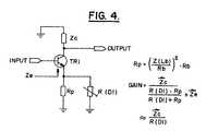
- Fig. 3the circuit of Fig. 1 has been modified by inserting an inductor Lb between emitter electrode of TR1 and resistor Rb.
- the size of inductor Lbis chosen so that it transforms the combined impedances of Lb and Rb to a high impedance "Rp" at the IF frequencies seen at node 14.
- Node 14is further connected through a coupling capacitor Ck (which can be regarding as a short circuit at the IF operating frequencies) to a shunt capacitor Ct and to a node 15 between an inductor Ld and a PIN diode D1.
- PIN diode D1in a known manner, acts as a resistor with a linear resistance characteristic at high frequencies.
- IdDC control current
- control terminal 16the RF resistance of PIN diode D1 can be varied accordingly.
- Inductor Ldprovides RF isolation for control input 16 and coupling capacitor Ck separates the bias circuits of transistor TR1 and PIN diode D1 and, as above indicated, is essentially a short circuit at the IF bandwidth seen by the circuit.
- Capacitor Ckmay be sized so as to tune out stray inductances that appear from the emitter of TR1, through diode D1 to ground thereby decreasing the effective value of Ze.
- Capacitor Ctwhich includes the stray capacitances Cp (from Fig. 1) is employed to tune out the imaginary portions of the impedances of Lb and Ld.
- the emitter impedance Rpis much greater than R(D1), as required.
- the value of Rpmay be chosen so that the slope of the gain control characteristic is the same at both minimum and maximum gain ranges. Rp will, in this manner, change the control slope at low gains in the same manner that Ze changes the slope at high gain levels. Thus, Rp acts as a linearizer. Even in this case, however, the value of Rp is higher Rb.
Landscapes
- Control Of Amplification And Gain Control (AREA)
Description
Claims (9)
- A circuit for amplifying RF signals having a substantiallylinear gain characteristic responsive to a control signal, saidcircuit comprising:a transistor (TR1) having RF signals applied to an inputnode (10) thereof, an amplified signal present at an outputnode (12) thereof, and a transistor control node (14);complex impedance means (Lb,Rb) electrically coupled between thetransistor control node and a source of common potential;reactance means (Cf) electrically coupled in parallel acrossthe complex impedance means for providing for the RF signals asubstantially resonant parallel circuit electrically coupled tothe transistor control node; anddiode means (D1) electrically coupled between thetransistor control node and the source of common potential andresponsive to the control signal for varying the transistorcontrol node impedance of the circuit and thereby varying thegain of the circuit.
- A circuit according to claim 1, wherein the RF signalscomprise a band of RF signals.
- A circuit according to claim 1 or claim 2, wherein thetransistor (TR1) is a bipolar transistor, and the input node(10) is electrically coupled to a base circuit, the output node(12) is electrically coupled to a collector circuit and thetransistor control node (14) is electrically coupled to an emitter circuit of the bipolar transistor .
- A circuit according to claim 1 or claim 2, wherein thetransistor (TR1) is a field effect transistor (FET), and theinput node (10) is electrically coupled to a gate circuit, theoutput node (12) is electrically coupled to a drain circuit andthe transistor control node is electrically coupled to a sourcecircuit of the FET.
- A circuit according to any preceding claim, wherein thesubstantially resonant parallel circuit provides an impedancethat is substantially greater than the variable resistance ofthe diode means (D1).
- A circuit according to any preceding claim, wherein thecomplex impedance means is a resistor (Rb) series coupled to afirst inductor (Lb).
- A circuit according to any preceding claim, wherein saiddiode means (D1) is a PIN diode having an anode thereofelectrically coupled both to the transistor control node (14)and to a source of control signal via a second inductor (Ld).
- A circuit according to any preceding claim, wherein thereactance means is a capacitor.
- A circuit according to any preceding claim, wherein thegain is measured in decibels and the control signal is alogarithmic control signal.
Applications Claiming Priority (2)
| Application Number | Priority Date | Filing Date | Title |
|---|---|---|---|
| US07/989,117US5307026A (en) | 1992-12-11 | 1992-12-11 | Variable gain RF amplifier with linear gain control |
| US989117 | 1992-12-11 |
Publications (3)
| Publication Number | Publication Date |
|---|---|
| EP0601888A2 EP0601888A2 (en) | 1994-06-15 |
| EP0601888A3 EP0601888A3 (en) | 1995-06-14 |
| EP0601888B1true EP0601888B1 (en) | 1998-10-14 |
Family
ID=25534780
Family Applications (1)
| Application Number | Title | Priority Date | Filing Date |
|---|---|---|---|
| EP93310004AExpired - LifetimeEP0601888B1 (en) | 1992-12-11 | 1993-12-10 | Variable gain RF amplifier with linear gain control |
Country Status (3)
| Country | Link |
|---|---|
| US (1) | US5307026A (en) |
| EP (1) | EP0601888B1 (en) |
| DE (1) | DE69321565T2 (en) |
Cited By (1)
| Publication number | Priority date | Publication date | Assignee | Title |
|---|---|---|---|---|
| CN102185572A (en)* | 2011-03-11 | 2011-09-14 | 京信通信系统(中国)有限公司 | Electrically-tuned gain equalizer circuit |
Families Citing this family (13)
| Publication number | Priority date | Publication date | Assignee | Title |
|---|---|---|---|---|
| DE69624673T2 (en)* | 1996-01-17 | 2003-09-18 | Nokia Corp., Espoo | Method for extending the range of a received signal strength indicator and radio transceiver operating according to this method |
| US6091301A (en)* | 1996-06-03 | 2000-07-18 | Scientific-Atlanta, Inc. | Flatness compensation of diplex filter roll-off using active amplifier peaking circuit |
| GB2318004A (en)* | 1996-10-01 | 1998-04-08 | Nokia Mobile Phones Ltd | A diode detector |
| US6553214B1 (en) | 1999-05-05 | 2003-04-22 | Tenatronics Limited | Active window glass antenna system with automatic overload protection circuit |
| US6271727B1 (en) | 1999-08-06 | 2001-08-07 | Rf Micro Devices, Inc. | High isolation RF power amplifier with self-bias attenuator |
| US7545774B1 (en) | 1999-08-26 | 2009-06-09 | Nokia Corporation | Method for indicating power consumption in a packet switched communication system |
| DE10050740B4 (en)* | 2000-10-13 | 2010-10-14 | Rohde & Schwarz Gmbh & Co. Kg | amplifier |
| US6766153B2 (en) | 2001-04-02 | 2004-07-20 | Itran Communications Ltd. | Dynamic automatic gain control circuit employing kalman filtering |
| US6906592B2 (en) | 2002-11-13 | 2005-06-14 | Qualcomm Inc | Continuously variable gain radio frequency driver amplifier having linear in decibel gain control characteristics |
| US8381074B1 (en)* | 2010-05-21 | 2013-02-19 | Lsi Corporation | Systems and methods for utilizing a centralized queue based data processing circuit |
| US9985592B2 (en)* | 2015-05-13 | 2018-05-29 | Skyworks Solutions, Inc. | High gain RF power amplifier with negative capacitor |
| CN106067772B (en)* | 2016-06-12 | 2018-05-18 | 广州杰赛科技股份有限公司 | The gain compensating method and device of a kind of radio-frequency module |
| CN106100599B (en)* | 2016-06-12 | 2018-11-23 | 广州杰赛科技股份有限公司 | A kind of gain compensating method and device of radio-frequency module |
Family Cites Families (6)
| Publication number | Priority date | Publication date | Assignee | Title |
|---|---|---|---|---|
| US3023369A (en)* | 1959-02-09 | 1962-02-27 | Blonder Tongue Elect | Variable-gain transistor circuit |
| DE1537690C3 (en)* | 1967-09-20 | 1975-02-13 | Siemens Ag, 1000 Berlin Und 8000 Muenchen | Transistor-equipped broadband amplifier with gain control |
| FR2204333A5 (en)* | 1972-10-20 | 1974-05-17 | Thomson Csf | |
| JPS57135510A (en)* | 1981-02-17 | 1982-08-21 | Toshiba Corp | Gain control circuit |
| JPS60181913U (en)* | 1984-05-14 | 1985-12-03 | アルプス電気株式会社 | gain control circuit |
| US4677392A (en)* | 1985-12-16 | 1987-06-30 | Hughes Aircraft Company | Cascaded internal impedance dependent amplifier with accurate variable gain control |
- 1992
- 1992-12-11USUS07/989,117patent/US5307026A/ennot_activeExpired - Lifetime
- 1993
- 1993-12-10DEDE69321565Tpatent/DE69321565T2/ennot_activeExpired - Fee Related
- 1993-12-10EPEP93310004Apatent/EP0601888B1/ennot_activeExpired - Lifetime
Cited By (1)
| Publication number | Priority date | Publication date | Assignee | Title |
|---|---|---|---|---|
| CN102185572A (en)* | 2011-03-11 | 2011-09-14 | 京信通信系统(中国)有限公司 | Electrically-tuned gain equalizer circuit |
Also Published As
| Publication number | Publication date |
|---|---|
| EP0601888A2 (en) | 1994-06-15 |
| US5307026A (en) | 1994-04-26 |
| EP0601888A3 (en) | 1995-06-14 |
| DE69321565D1 (en) | 1998-11-19 |
| DE69321565T2 (en) | 1999-05-06 |
Similar Documents
| Publication | Publication Date | Title |
|---|---|---|
| EP0601888B1 (en) | Variable gain RF amplifier with linear gain control | |
| KR100816217B1 (en) | Gain variable amplifier | |
| US5272450A (en) | DC feed network for wideband RF power amplifier | |
| EP0886384A2 (en) | Single-stage dual-band low-noise amplifier for use in a wireless communication system receiver | |
| US4367443A (en) | Radio frequency signal power amplifier | |
| US5661437A (en) | Negative feedback variable gain amplifier circuit | |
| JPH08181544A (en) | Microwave predistorted linearization circuit | |
| KR20020059355A (en) | Radio frequency device with fast charging of an input capacitance | |
| US6624700B2 (en) | Radio frequency power amplifier for cellular telephones | |
| US5694085A (en) | High-power amplifier using parallel transistors | |
| US5343172A (en) | Variable reactance circuit for microwave or millimeter wave band and variable matching circuit using variable reactance circuit | |
| US6630861B2 (en) | Variable gain amplifier | |
| US5339048A (en) | Radio frequency amplifier | |
| JPH0211005A (en) | Unconditionally stable extra-low noise rf preamplifier | |
| US5304948A (en) | RF amplifier with linear gain control | |
| EP0250453B1 (en) | Cascaded internal impedance dependent amplifier with accurate variable gain control | |
| US5565823A (en) | Voltage controlled attenuator using PN diodes | |
| US20030020546A1 (en) | Active element bias circuit for RF power transistor input | |
| US6400222B1 (en) | Linearizer | |
| US4048578A (en) | R.f. amplifier circuit | |
| JP2606165B2 (en) | Impedance matching circuit | |
| EP0438257A2 (en) | High frequency amplifier | |
| KR200308685Y1 (en) | Low noise amplifier | |
| JP4017870B2 (en) | Low noise amplifier | |
| US20240258976A1 (en) | Automatic rf output power-limiting amplifier with dynamic feedback |
Legal Events
| Date | Code | Title | Description |
|---|---|---|---|
| PUAI | Public reference made under article 153(3) epc to a published international application that has entered the european phase | Free format text:ORIGINAL CODE: 0009012 | |
| AK | Designated contracting states | Kind code of ref document:A2 Designated state(s):DE FR GB SE | |
| RIN1 | Information on inventor provided before grant (corrected) | Inventor name:MUCKE, LARS H. | |
| PUAL | Search report despatched | Free format text:ORIGINAL CODE: 0009013 | |
| AK | Designated contracting states | Kind code of ref document:A3 Designated state(s):DE FR GB SE | |
| 17P | Request for examination filed | Effective date:19951214 | |
| GRAG | Despatch of communication of intention to grant | Free format text:ORIGINAL CODE: EPIDOS AGRA | |
| 17Q | First examination report despatched | Effective date:19980115 | |
| GRAG | Despatch of communication of intention to grant | Free format text:ORIGINAL CODE: EPIDOS AGRA | |
| GRAH | Despatch of communication of intention to grant a patent | Free format text:ORIGINAL CODE: EPIDOS IGRA | |
| GRAH | Despatch of communication of intention to grant a patent | Free format text:ORIGINAL CODE: EPIDOS IGRA | |
| GRAA | (expected) grant | Free format text:ORIGINAL CODE: 0009210 | |
| AK | Designated contracting states | Kind code of ref document:B1 Designated state(s):DE FR GB SE | |
| REF | Corresponds to: | Ref document number:69321565 Country of ref document:DE Date of ref document:19981119 | |
| ET | Fr: translation filed | ||
| PLBE | No opposition filed within time limit | Free format text:ORIGINAL CODE: 0009261 | |
| STAA | Information on the status of an ep patent application or granted ep patent | Free format text:STATUS: NO OPPOSITION FILED WITHIN TIME LIMIT | |
| 26N | No opposition filed | ||
| REG | Reference to a national code | Ref country code:GB Ref legal event code:IF02 | |
| REG | Reference to a national code | Ref country code:GB Ref legal event code:732E | |
| PGFP | Annual fee paid to national office [announced via postgrant information from national office to epo] | Ref country code:SE Payment date:20031204 Year of fee payment:11 | |
| PGFP | Annual fee paid to national office [announced via postgrant information from national office to epo] | Ref country code:GB Payment date:20031210 Year of fee payment:11 Ref country code:FR Payment date:20031210 Year of fee payment:11 | |
| PGFP | Annual fee paid to national office [announced via postgrant information from national office to epo] | Ref country code:DE Payment date:20031218 Year of fee payment:11 | |
| PG25 | Lapsed in a contracting state [announced via postgrant information from national office to epo] | Ref country code:GB Free format text:LAPSE BECAUSE OF NON-PAYMENT OF DUE FEES Effective date:20041210 | |
| PG25 | Lapsed in a contracting state [announced via postgrant information from national office to epo] | Ref country code:SE Free format text:LAPSE BECAUSE OF NON-PAYMENT OF DUE FEES Effective date:20041211 | |
| PG25 | Lapsed in a contracting state [announced via postgrant information from national office to epo] | Ref country code:DE Free format text:LAPSE BECAUSE OF NON-PAYMENT OF DUE FEES Effective date:20050701 | |
| EUG | Se: european patent has lapsed | ||
| GBPC | Gb: european patent ceased through non-payment of renewal fee | Effective date:20041210 | |
| PG25 | Lapsed in a contracting state [announced via postgrant information from national office to epo] | Ref country code:FR Free format text:LAPSE BECAUSE OF NON-PAYMENT OF DUE FEES Effective date:20050831 | |
| REG | Reference to a national code | Ref country code:FR Ref legal event code:ST |