EP0598422A1 - Method of forming a Ti and a TiN layer on a semiconductor body by a sputtering process, comprising an additional step of cleaning the target - Google Patents
Method of forming a Ti and a TiN layer on a semiconductor body by a sputtering process, comprising an additional step of cleaning the targetDownload PDFInfo
- Publication number
- EP0598422A1 EP0598422A1EP93202840AEP93202840AEP0598422A1EP 0598422 A1EP0598422 A1EP 0598422A1EP 93202840 AEP93202840 AEP 93202840AEP 93202840 AEP93202840 AEP 93202840AEP 0598422 A1EP0598422 A1EP 0598422A1
- Authority
- EP
- European Patent Office
- Prior art keywords
- layer
- target
- process step
- during
- additional process
- Prior art date
- Legal status (The legal status is an assumption and is not a legal conclusion. Google has not performed a legal analysis and makes no representation as to the accuracy of the status listed.)
- Granted
Links
Images


Classifications
- H—ELECTRICITY
- H01—ELECTRIC ELEMENTS
- H01L—SEMICONDUCTOR DEVICES NOT COVERED BY CLASS H10
- H01L21/00—Processes or apparatus adapted for the manufacture or treatment of semiconductor or solid state devices or of parts thereof
- H01L21/70—Manufacture or treatment of devices consisting of a plurality of solid state components formed in or on a common substrate or of parts thereof; Manufacture of integrated circuit devices or of parts thereof
- H01L21/71—Manufacture of specific parts of devices defined in group H01L21/70
- H01L21/768—Applying interconnections to be used for carrying current between separate components within a device comprising conductors and dielectrics
- H01L21/76838—Applying interconnections to be used for carrying current between separate components within a device comprising conductors and dielectrics characterised by the formation and the after-treatment of the conductors
- H01L21/76841—Barrier, adhesion or liner layers
- H01L21/76843—Barrier, adhesion or liner layers formed in openings in a dielectric
- C—CHEMISTRY; METALLURGY
- C23—COATING METALLIC MATERIAL; COATING MATERIAL WITH METALLIC MATERIAL; CHEMICAL SURFACE TREATMENT; DIFFUSION TREATMENT OF METALLIC MATERIAL; COATING BY VACUUM EVAPORATION, BY SPUTTERING, BY ION IMPLANTATION OR BY CHEMICAL VAPOUR DEPOSITION, IN GENERAL; INHIBITING CORROSION OF METALLIC MATERIAL OR INCRUSTATION IN GENERAL
- C23C—COATING METALLIC MATERIAL; COATING MATERIAL WITH METALLIC MATERIAL; SURFACE TREATMENT OF METALLIC MATERIAL BY DIFFUSION INTO THE SURFACE, BY CHEMICAL CONVERSION OR SUBSTITUTION; COATING BY VACUUM EVAPORATION, BY SPUTTERING, BY ION IMPLANTATION OR BY CHEMICAL VAPOUR DEPOSITION, IN GENERAL
- C23C14/00—Coating by vacuum evaporation, by sputtering or by ion implantation of the coating forming material
- C23C14/0021—Reactive sputtering or evaporation
- C23C14/0036—Reactive sputtering
- C23C14/0073—Reactive sputtering by exposing the substrates to reactive gases intermittently
- C—CHEMISTRY; METALLURGY
- C23—COATING METALLIC MATERIAL; COATING MATERIAL WITH METALLIC MATERIAL; CHEMICAL SURFACE TREATMENT; DIFFUSION TREATMENT OF METALLIC MATERIAL; COATING BY VACUUM EVAPORATION, BY SPUTTERING, BY ION IMPLANTATION OR BY CHEMICAL VAPOUR DEPOSITION, IN GENERAL; INHIBITING CORROSION OF METALLIC MATERIAL OR INCRUSTATION IN GENERAL
- C23C—COATING METALLIC MATERIAL; COATING MATERIAL WITH METALLIC MATERIAL; SURFACE TREATMENT OF METALLIC MATERIAL BY DIFFUSION INTO THE SURFACE, BY CHEMICAL CONVERSION OR SUBSTITUTION; COATING BY VACUUM EVAPORATION, BY SPUTTERING, BY ION IMPLANTATION OR BY CHEMICAL VAPOUR DEPOSITION, IN GENERAL
- C23C14/00—Coating by vacuum evaporation, by sputtering or by ion implantation of the coating forming material
- C23C14/02—Pretreatment of the material to be coated
- C23C14/021—Cleaning or etching treatments
- C23C14/022—Cleaning or etching treatments by means of bombardment with energetic particles or radiation
- C—CHEMISTRY; METALLURGY
- C23—COATING METALLIC MATERIAL; COATING MATERIAL WITH METALLIC MATERIAL; CHEMICAL SURFACE TREATMENT; DIFFUSION TREATMENT OF METALLIC MATERIAL; COATING BY VACUUM EVAPORATION, BY SPUTTERING, BY ION IMPLANTATION OR BY CHEMICAL VAPOUR DEPOSITION, IN GENERAL; INHIBITING CORROSION OF METALLIC MATERIAL OR INCRUSTATION IN GENERAL
- C23C—COATING METALLIC MATERIAL; COATING MATERIAL WITH METALLIC MATERIAL; SURFACE TREATMENT OF METALLIC MATERIAL BY DIFFUSION INTO THE SURFACE, BY CHEMICAL CONVERSION OR SUBSTITUTION; COATING BY VACUUM EVAPORATION, BY SPUTTERING, BY ION IMPLANTATION OR BY CHEMICAL VAPOUR DEPOSITION, IN GENERAL
- C23C14/00—Coating by vacuum evaporation, by sputtering or by ion implantation of the coating forming material
- C23C14/06—Coating by vacuum evaporation, by sputtering or by ion implantation of the coating forming material characterised by the coating material
- C23C14/0641—Nitrides
- C—CHEMISTRY; METALLURGY
- C23—COATING METALLIC MATERIAL; COATING MATERIAL WITH METALLIC MATERIAL; CHEMICAL SURFACE TREATMENT; DIFFUSION TREATMENT OF METALLIC MATERIAL; COATING BY VACUUM EVAPORATION, BY SPUTTERING, BY ION IMPLANTATION OR BY CHEMICAL VAPOUR DEPOSITION, IN GENERAL; INHIBITING CORROSION OF METALLIC MATERIAL OR INCRUSTATION IN GENERAL
- C23C—COATING METALLIC MATERIAL; COATING MATERIAL WITH METALLIC MATERIAL; SURFACE TREATMENT OF METALLIC MATERIAL BY DIFFUSION INTO THE SURFACE, BY CHEMICAL CONVERSION OR SUBSTITUTION; COATING BY VACUUM EVAPORATION, BY SPUTTERING, BY ION IMPLANTATION OR BY CHEMICAL VAPOUR DEPOSITION, IN GENERAL
- C23C14/00—Coating by vacuum evaporation, by sputtering or by ion implantation of the coating forming material
- C23C14/06—Coating by vacuum evaporation, by sputtering or by ion implantation of the coating forming material characterised by the coating material
- C23C14/14—Metallic material, boron or silicon
- C23C14/16—Metallic material, boron or silicon on metallic substrates or on substrates of boron or silicon
- C23C14/165—Metallic material, boron or silicon on metallic substrates or on substrates of boron or silicon by cathodic sputtering
- H—ELECTRICITY
- H01—ELECTRIC ELEMENTS
- H01L—SEMICONDUCTOR DEVICES NOT COVERED BY CLASS H10
- H01L21/00—Processes or apparatus adapted for the manufacture or treatment of semiconductor or solid state devices or of parts thereof
- H01L21/70—Manufacture or treatment of devices consisting of a plurality of solid state components formed in or on a common substrate or of parts thereof; Manufacture of integrated circuit devices or of parts thereof
- H01L21/71—Manufacture of specific parts of devices defined in group H01L21/70
- H01L21/768—Applying interconnections to be used for carrying current between separate components within a device comprising conductors and dielectrics
- H01L21/76838—Applying interconnections to be used for carrying current between separate components within a device comprising conductors and dielectrics characterised by the formation and the after-treatment of the conductors
- H01L21/76841—Barrier, adhesion or liner layers
Definitions
- the inventionrelates to a method of manufacturing semiconductor devices whereby first a Ti layer and then a TiN layer is deposited on slices of semiconductor material in that the slices are placed on a support one after the other in a deposition chamber, which support is arranged opposite a target of Ti surrounded by an annular anode, and in that then material is sputtered off the target by means of a plasma which is generated near the target in Ar during the deposition of the Ti layer and in a gas mixture of Ar and N2 during the deposition of the TiN layer, after which the target is cleaned in an additional process step by sputtering off of material from the target by means of a plasma generated in Ar each time before a next slice is placed in the chamber.
- a metallizationcomprising a Ti layer, a TiN layer and a further conductive layer is often provided on a surface of a semiconductor body.
- the Ti layerthen serves to obtain a good adhesion and a low contact resistance between the metallization and the semiconductor body.
- the TiN layerserves as a barrier to prevent chemical reactions of the Al with the Ti and the semiconductor material situated underneath the barrier layer.
- the TiNserves as a barrier to prevent chemical reactions between Ti and F which is formed during such a CVD process.
- the depositionsare carried out in practice on slices of semiconductor material which are broken or sawn into a large number of separate semiconductor bodies at a later stage.
- a sliceis passed through an input station into a first deposition chamber of a sputter deposition device, where the Ti and TiN layers are deposited by the method described above, after which the slice is transported to a second deposition chamber in which, for example, an Al or W layer is deposited, and finally the slice is taken from the device through an output station.
- a slice leaves a deposition chambera new slice is immediately introduced into the chamber in practice.
- a plasmais generated in a gas mixture comprising Ar and N2 near the target.
- a top layer comprising nitrogenis created thereby on the target during this deposition step.
- Materialis sputtered off this target during the extra process step, which material is then deposited on the slice.
- a Ti layer comprising nitrogenis deposited on the slice, which layer initially consists of TiN and in which the nitrogen occurs in a decreasing concentration seen in the thickness direction of the layer.
- the layeraccordingly merges well with a TiN layer. If such a layer were deposited on the next slice instead of the Ti layer as a first layer of a metallization, then this metallization thereon would on the contrary exhibit a bad adhesion and a high contact resistance.
- a conductive top layer of Al or Al alloyed with a few percents of Si or Cuis provided thereon, the Al and Ti react with one another, forming compounds with a comparatively high electric resistance. A good adhesion is then indeed obtained, but the conductive Al layer must then be provided to a comparatively great thickness in order to ensure that conductor tracks having a comparatively low resistance can be formed in the layer structure thus created.
- a W layeris deposited on the said layer comprising free Ti by means of a usual CVD process (chemical deposition process) in which WF6 is used, then the free Ti reacts with F formed during such a CVD process. This leads to the formation of TiF3, to which W has a bad adhesion.
- the inventionhas for its object inter alia to provide a method in which the said disadvantages are counteracted as much as possible.
- the method mentioned in the opening paragraphis for this purpose characterized in that the additional process step is ended as soon as the target exhibits a clean Ti surface again. It is achieved by this that the Ti layer deposited as a first layer on a slice consists of pure Ti and accordingly has a good adhesion to this slice and a low contact resistance.
- the said necessary additional process steptakes as little time as possible in that cleaning of the target is ended as soon as it has a clean Ti surface.
- An additional layer of Ti comprising nitrogenis indeed deposited on the TiN layer during this additional process step, but this additional layer is as thin as possible and accordingly comprises as little free Ti as possible.
- a constant electric poweris supplied to the plasma during the additional process step, whereby a changing voltage arises between target and anode, which voltage reaches an end value which does not change any more during the additional process step, which end value is used for ending the additional process step.
- the voltage arising between target and anode during the additional process stepmay be simply measured with a voltmeter. This voltage changes as long as the target still exhibits a surface of Ti comprising nitrogen, but reaches an end value as soon as the target exhibits a clean Ti surface again.
- this end valuemay be readily ascertained in that the sputtering-off of the target is continued once for a period longer than necessary. It can then be ascertained in a simple manner through measurement of the voltage between target and anode when the target has been cleaned.
- the targetWhen the additional process step is now stopped each time after the period thus ascertained has elapsed, the target will always exhibit the desired clean Ti surface after this process step.
- This methodis not very practical.
- the voltage between the target and the anodeis measured during the additional process step and this process step is ended as soon as this voltage has reached the said end value.
- a comparatively great electric poweris supplied to the plasma in practice during the deposition of the TiN layer, for example, more than 6 kW.
- a constant electric poweris supplied to the plasma during the additional process step which is smaller than the power supplied to the plasma during deposition of the TiN layer.
- a flow of Aris led into the deposition chamber during the additional process step which is greater than that which is led into the deposition chamber as part of the gas mixture of Ar and N2 during the deposition of the TiN layer.
- the voltage between target and anodewill reach a lower end value, while in addition the change of this voltage during the additional process step is greater.
- Figs. 1 to 3diagrammatically and in cross-section show a few stages of manufacture of a semiconductor device with a semiconductor body 1 of, for example, n-type doped monocrystalline Si in which field oxide regions 2 and p-type doped semiconductor zones 3 adjoining the surface 4 are provided in usual manner.
- Conductor tracks 5 of polycrystalline Siare provided on the surface 4.
- the surface 4is provided with an insulating layer 6 of, for example, silicon oxide, silicon nitride, or silicon oxynitride.
- Windows 7are provided in the insulating layer 6 for contacting silicon regions situated below the insulating layer 6. These silicon regions may be regions of monocrystalline silicon which may or may not be provided with a top layer of a metal silicide.
- a package of layers 8, 9, 10is provided on the insulating layer 6 and in the contact window 7, comprising a Ti layer 8, a TiN layer 9, and a further conductive top layer 10.
- the Ti layer 8then serves to obtain a good adhesion between the layer package 8, 9, 10 and the semiconductor zone 3 plus the insulating layer 6, and to obtain a low contact resistance between the layer package 8, 9, 10 and the semiconductor zone 3.
- the TiN layer 3serves as a barrier to prevent chemical reactions of the Al with the Ti and the semiconductor material situated below the barrier layer.
- the TiN layerserves as a barrier to prevent chemical reactions between Ti and F which is formed during such a CVD process.
- a layer of silicon oxide 12is deposited in a plasma deposition process (PECVD), a layer of spin-on glass (SOG) 13 is deposited by a spin-on method, and then a layer of silicon oxide 14 is provided in a plasma deposition process (PECVD) again.
- Contact windows 15are provided in the layer package 12, 13, 14 so that a conductor pattern 16 provided on the package makes contact with the Al top layer 10. Since the use of the layer of spin-on glass 13 in the layer package 12, 13, 14 has a smoothing effect, the upper silicon oxide layer 14 is comparatively plane.
- the field oxide regions 2 and the semiconductor zones 3are provided in slices of semiconductor material, which will be broken or sawn into a large number of separate semiconductor bodies 1 in a later stage, and provided with the insulating layer 6 with contact windows 7. Then first a Ti layer and subsequently a TiN layer are deposited on these slices.
- a slice 20is introduced into a first deposition chamber 22 of a sputter deposition device 23 through an input station 21 in this case, the Ti and TiN layers being deposited in this chamber, after which the slice is transported to a second deposition chamber 24 in which, for example, a layer of Al or W is deposited, and finally the slice is taken from the device again through an output station 25.
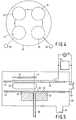
- FIG. 5diagrammatically shows a cross-section through the deposition chamber 22 in which the Ti and TiN layers are deposited on the slices 20.
- the slices 20 with a diameter of approximately 15 cmare for this purpose placed in the deposition chamber 22 on a support 30 which is arranged at a distance of approximately 5 cm opposite a Ti target 32 of approximately 26 cm diameter surrounded by an annular anode 31.
- An earthed screen 33is provided around the support. Then a gas or gas mixture is led into the deposition chamber 22 through a feed line 34.
- An electric supply source 45is connected between the target 32 and the annular anode 31 whereby a plasma 35 is generated in the gas or gas mixture, which plasma is enclosed between the target 32 and the slice 20 and in the vicinity of the target 32 by means of magnets 36 arranged behind the target 32.
- the magnets 36are jointly rotatable about an axis 37. In practice, they rotate about the axis 37 a few times each second during the deposition process, so that the plasma 35 is rotated about the same axis 37. It is achieved thereby that atoms are homogeneously sputtered off the entire surface of the target 32, so that also a homogeneous deposition all over the slice 20 is obtained.
- the slice 20is cooled during deposition in that a gas cushion 38 with a pressure of 100 to 2000 Pa is maintained between the support 30 and the semiconductor slice 20.
- Aris conducted to between the support 30 and the slice 20 through a gas line 39.
- the support 30is provided with a rim 40 against which the slice 20 is pressed by clamps (not shown). Leakage of Ar from the gas cushion 38 into the deposition chamber 22 is limited by this.
- the support 30is kept at a temperature of 200 to 400° C during the deposition of the Ti and TiN layers by usual means (not shown).
- the chamber 22is further provided with a gas outlet 43 which is connected to a pump (not shown) by which gases can be discharged and by which the reaction chamber 22 can be maintained at a desired pressure.
- materialis sputtered off the target 32 by the plasma 35 which is generated near the target 32 in Ar during the deposition of the Ti layer and in a gas mixture of Ar and N2 during the deposition of the TiN layer.
- the target 32is cleaned each time before a next slice 20 is placed in the chamber 22 in that material is sputtered off the target 32 by means of a plasma generated in Ar.
- a plasma 35is generated near the target 32 in a gas mixture comprising Ar and N2 during the deposition of the TiN layer 9. This results in a top layer comprising nitrogen (not shown) on the target 32 during this deposition step.
- material from this target 32is deposited on the slice 20.
- a layer of Ti comprising nitrogen(not shown) is deposited on the slice, which layer initially consists of TiN and in which the nitrogen is present in a decreasing concentration seen in the thickness direction of the layer.
- the layeraccordingly merges well with a TiN layer. If such a layer were to be deposited on the next slice as a first layer of a metallization instead of the Ti layer, this metallization would indeed exhibit a bad adhesion thereto and a high contact resistance.
- the additional process stepis ended the moment the target 32 shows a clean Ti surface again. It is achieved by this that the Ti layer 8 deposited as a first layer on a slice 20 consists of pure Ti and accordingly has a good adhesion to this slice 20.
- This necessary additional process stepis as short as possible owing to the fact that cleaning of the target 32 is ended the moment it shows a clean Ti surface. It is true that a layer of Ti comprising nitrogen is deposited on the TiN layer during this additional process step, but this layer is as thin as possible and accordingly contains as little free Ti as possible.
- a conductive top layer of Al or of an alloy of Al with a few percents of Si or Cuis provided on this layer, the Al and Ti react with one another, forming compounds which have a comparatively high electrical resistance. A good adhesion is then indeed obtained, but the conductive Al layer must then be provided to a comparatively great thickness in order to ensure that conductor tracks having a comparatively low resistance can be formed in the layer package thus formed.
- FIG. 7shows a graph of the end values V e as a function of the pressure p with which Ar was led into the deposition chamber, with electric powers of 0.3 kW, 0.5 kW, 1kW and 2 kW being supplied to the plasma as indicated by the curves 55, 56, 57 and 58. It is found that the voltage V t reaches an end value V e which does not change any more and which is dependent on the pressure p with which Ar is led into the reaction chamber and on the power supplied to the plasma. The end value V e is used for ending the additional process step. In the cases indicated above, a layer of Ti comprising nitrogen of a thickness of 8 to 10 nm is found to have been deposited during the additional process step each time.
- the voltage V tmay be simply measured with a voltmeter 44 in Fig. 5. This voltage changes as long as the target 32 still has a surface of Ti comprising nitrogen, but reaches an end value V e the moment the target 32 shows a clean Ti surface again. A selection is made as to what electric power will be supplied to the plasma and with what pressure Ar will be conducted into the deposition chamber in order to achieve that the additional process step can be carried out in a desired time. The end value V e may then be readily determined in that sputtering off of the target 32 is continued once for a longer period than necessary under these chosen process conditions. It can subsequently be ascertained in a simple manner through measurement of the voltage V t after what time the target had become clean.
- the targetWhen the additional process step is now stopped after the time thus ascertained has elapsed, the target will always have the desired clean Ti surface after this process step.
- This methodis not very practical.
- the electric voltage between the target and the anodeis measured during the additional process step and this process step is ended the moment this voltage has reached the said end value.
- a comparatively high electric powerfor example more than 6 kW, is supplied to the plasma in practice during the deposition of the TiN layer in order to deposit the TiN layer in a practical time of, for example, less than 60 seconds.
- a constant electric power smaller than the power supplied to the plasma during the deposition of the TiN layeris supplied to the plasma during the additional process step.
- the voltage between target and anodethen reaches the said end value in a so much shorter time than if the electric power were not reduced that it can be ascertained by simple means when the additional process step is to be ended. Without the measure, the step would have to be ended in practice, for example, after approximately 0.5 second, and with the measure, for example, after the more practical times mentioned above. Comparatively small flows of 5 sccm Ar and 15 sccm N2 are led into the deposition chamber during the deposition of the TiN layer in order to obtain a TiN layer with a substantially stoichiometric composition.
- a flow of Aris led into the deposition chamber during the additional process step which is greater than the flow led into the deposition chamber during the deposition of the TiN layer as part of the gas mixture of Ar and N2.
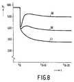
- Fig. 8like Fig. 6, shows the gradient of the voltage V t for the case in which a power of 0.5 kW was supplied to the plasma during the additional process step.
- Curve 51 in Fig. 8again indicates how V t changes when Ar is led into the deposition chamber at a pressure of 1.60 Pa.
- Curves 59 and 60show the gradient when Ar is led into the deposition chamber at a pressure of 0.25 Pa and 0.13 Pa, respectively.
Landscapes
- Chemical & Material Sciences (AREA)
- Engineering & Computer Science (AREA)
- Organic Chemistry (AREA)
- Materials Engineering (AREA)
- Mechanical Engineering (AREA)
- Metallurgy (AREA)
- Chemical Kinetics & Catalysis (AREA)
- Physics & Mathematics (AREA)
- Condensed Matter Physics & Semiconductors (AREA)
- General Physics & Mathematics (AREA)
- Manufacturing & Machinery (AREA)
- Computer Hardware Design (AREA)
- Microelectronics & Electronic Packaging (AREA)
- Power Engineering (AREA)
- Electrodes Of Semiconductors (AREA)
Abstract
Description
- The invention relates to a method of manufacturing semiconductor devices whereby first a Ti layer and then a TiN layer is deposited on slices of semiconductor material in that the slices are placed on a support one after the other in a deposition chamber, which support is arranged opposite a target of Ti surrounded by an annular anode, and in that then material is sputtered off the target by means of a plasma which is generated near the target in Ar during the deposition of the Ti layer and in a gas mixture of Ar and N₂ during the deposition of the TiN layer, after which the target is cleaned in an additional process step by sputtering off of material from the target by means of a plasma generated in Ar each time before a next slice is placed in the chamber.
In modem IC technology, a metallization comprising a Ti layer, a TiN layer and a further conductive layer is often provided on a surface of a semiconductor body. The Ti layer then serves to obtain a good adhesion and a low contact resistance between the metallization and the semiconductor body. When a layer of Al or of Al alloyed with a few percents of Si or Cu is used as the conductive top layer, the TiN layer serves as a barrier to prevent chemical reactions of the Al with the Ti and the semiconductor material situated underneath the barrier layer. With the use of W as a conductive layer, which is deposited by means of a usual CVD process (chemical deposition process) for which WF₆ is used, the TiN serves as a barrier to prevent chemical reactions between Ti and F which is formed during such a CVD process.
The depositions are carried out in practice on slices of semiconductor material which are broken or sawn into a large number of separate semiconductor bodies at a later stage. A slice is passed through an input station into a first deposition chamber of a sputter deposition device, where the Ti and TiN layers are deposited by the method described above, after which the slice is transported to a second deposition chamber in which, for example, an Al or W layer is deposited, and finally the slice is taken from the device through an output station. When a slice leaves a deposition chamber, a new slice is immediately introduced into the chamber in practice. - During the deposition of the TiN layer, a plasma is generated in a gas mixture comprising Ar and N₂ near the target. A top layer comprising nitrogen is created thereby on the target during this deposition step. Material is sputtered off this target during the extra process step, which material is then deposited on the slice. Thus a Ti layer comprising nitrogen is deposited on the slice, which layer initially consists of TiN and in which the nitrogen occurs in a decreasing concentration seen in the thickness direction of the layer. The layer accordingly merges well with a TiN layer. If such a layer were deposited on the next slice instead of the Ti layer as a first layer of a metallization, then this metallization thereon would on the contrary exhibit a bad adhesion and a high contact resistance.
- "Eclipse Newsletter", 10, June/July 1992, discloses a method of the kind mentioned in the opening paragraph whereby the additional process step is continued for some time after cleaning of the target, so that another layer of pure Ti is deposited on the slice in addition to the Ti layer comprising nitrogen. This pure Ti layer serves to obtain a good adhesion with a further Al layer to be provided.
It is achieved by the known method that the layer deposited as a first layer on a slice has a good adhesion thereto and a low contact resistance because this layer consists of pure Ti owing to cleaning of the target. The known method has the disadvantage, however, that a further layer comprising free Ti is deposited on top of the TiN layer. If a conductive top layer of Al or Al alloyed with a few percents of Si or Cu is provided thereon, the Al and Ti react with one another, forming compounds with a comparatively high electric resistance. A good adhesion is then indeed obtained, but the conductive Al layer must then be provided to a comparatively great thickness in order to ensure that conductor tracks having a comparatively low resistance can be formed in the layer structure thus created. If a W layer is deposited on the said layer comprising free Ti by means of a usual CVD process (chemical deposition process) in which WF₆ is used, then the free Ti reacts with F formed during such a CVD process. This leads to the formation of TiF₃, to which W has a bad adhesion. - The invention has for its objectinter alia to provide a method in which the said disadvantages are counteracted as much as possible.
According to the invention, the method mentioned in the opening paragraph is for this purpose characterized in that the additional process step is ended as soon as the target exhibits a clean Ti surface again. It is achieved by this that the Ti layer deposited as a first layer on a slice consists of pure Ti and accordingly has a good adhesion to this slice and a low contact resistance. The said necessary additional process step takes as little time as possible in that cleaning of the target is ended as soon as it has a clean Ti surface. An additional layer of Ti comprising nitrogen is indeed deposited on the TiN layer during this additional process step, but this additional layer is as thin as possible and accordingly comprises as little free Ti as possible. The said disadvantages are thus counteracted as much as possible.
Preferably, a constant electric power is supplied to the plasma during the additional process step, whereby a changing voltage arises between target and anode, which voltage reaches an end value which does not change any more during the additional process step, which end value is used for ending the additional process step.
The voltage arising between target and anode during the additional process step may be simply measured with a voltmeter. This voltage changes as long as the target still exhibits a surface of Ti comprising nitrogen, but reaches an end value as soon as the target exhibits a clean Ti surface again. After it has been determined how the additional process step will carried out,i.e. what power will be supplied to the plasma and at what pressure Ar will be led into the deposition chamber, this end value may be readily ascertained in that the sputtering-off of the target is continued once for a period longer than necessary. It can then be ascertained in a simple manner through measurement of the voltage between target and anode when the target has been cleaned. - When the additional process step is now stopped each time after the period thus ascertained has elapsed, the target will always exhibit the desired clean Ti surface after this process step. This method is not very practical. Preferably, therefore, according to the invention, the voltage between the target and the anode is measured during the additional process step and this process step is ended as soon as this voltage has reached the said end value.
To render it possible to deposit the TiN layer in a practical period of, for example, less than one minute, a comparatively great electric power is supplied to the plasma in practice during the deposition of the TiN layer, for example, more than 6 kW. Preferably, according to the invention, a constant electric power is supplied to the plasma during the additional process step which is smaller than the power supplied to the plasma during deposition of the TiN layer. The voltage between target and anode then reaches the said end value in a period which is so much longer than if the electric power were not reduced that as a result simpler means can suffice for ascertaining when the additional process step should be ended. Without the measure this step would have to be ended in practice, for example, after approximately 1 second, and with the measure, for example, after approximately 10 seconds.
To obtain a TiN layer with a substantially stoichiometric composition, comparatively small flows of Ar and N₂ are led into the deposition chamber during the deposition of this layer. Preferably, according to the invention, a flow of Ar is led into the deposition chamber during the additional process step which is greater than that which is led into the deposition chamber as part of the gas mixture of Ar and N₂ during the deposition of the TiN layer. As a result, the voltage between target and anode will reach a lower end value, while in addition the change of this voltage during the additional process step is greater. Thus it can be determined more accurately when the additional process step is to be ended. - The invention will now be explained in more detail below by way of example with reference to a drawing and a few embodiments. In the drawing:
- Figs. 1 to 3 diagrammatically and in cross-section show a few stages of manufacture of a semiconductor device manufactured by the method according to the invention,
- Fig. 4 diagrammatically shows a sputter deposition device for carrying out the method according to the invention,
- Fig. 5 diagrammatically shows one of the deposition chambers in the device according to Fig. 4,
- Fig. 6 shows the gradient of the voltage Vt between the target and the anode from the moment t₀ at which the deposition of the TiN layer was ended, an electric power of 0.3 kW, 0.5 kW, 1 kW and 2 kW being supplied to the plasma,
- Fig. 7 shows the gradient of the end values Ve as a function of the pressure p with which Ar was led into the deposition chamber, an electric power of 0.3 kW, 0.5 kW, 1 kW and 2 kW being supplied to the plasma, and
- Fig. 8 shows the gradient of the voltage Vt with a power of 0.5 kW being supplied to the plasma and Ar being led into the deposition chamber at pressures of 1.60 Pa, 0.25 Pa and 0.13 Pa.
- Figs. 1 to 3 diagrammatically and in cross-section show a few stages of manufacture of a semiconductor device with a
semiconductor body 1 of, for example, n-type doped monocrystalline Si in whichfield oxide regions 2 and p-type dopedsemiconductor zones 3 adjoining thesurface 4 are provided in usual manner. Conductor tracks 5 of polycrystalline Si are provided on thesurface 4. Then thesurface 4 is provided with aninsulating layer 6 of, for example, silicon oxide, silicon nitride, or silicon oxynitride. Windows 7 are provided in theinsulating layer 6 for contacting silicon regions situated below theinsulating layer 6. These silicon regions may be regions of monocrystalline silicon which may or may not be provided with a top layer of a metal silicide.
Then a package oflayers insulating layer 6 and in thecontact window 7, comprising aTi layer 8, aTiN layer 9, and a furtherconductive top layer 10. TheTi layer 8 then serves to obtain a good adhesion between thelayer package semiconductor zone 3 plus theinsulating layer 6, and to obtain a low contact resistance between thelayer package semiconductor zone 3. When a layer of Al or of an alloy of Al with a few percents of Si or Cu is used as theconductive top layer 10, theTiN layer 3 serves as a barrier to prevent chemical reactions of the Al with the Ti and the semiconductor material situated below the barrier layer. When a W layer is used as theconductive top layer 10, deposited by means of a usual CVD process (chemical deposition process) in which WF₆ is used, the TiN layer serves as a barrier to prevent chemical reactions between Ti and F which is formed during such a CVD process.
After a pattern ofconductors 11 has been etched into thelayer package semiconductor zones 3 through thecontact windows 7, a package ofinsulating layers silicon oxide 14 is provided in a plasma deposition process (PECVD) again. Contact windows 15 are provided in thelayer package conductor pattern 16 provided on the package makes contact with the Altop layer 10. Since the use of the layer of spin-onglass 13 in thelayer package silicon oxide layer 14 is comparatively plane.
During the manufacture of the semiconductor devices, thefield oxide regions 2 and thesemiconductor zones 3 are provided in slices of semiconductor material, which will be broken or sawn into a large number ofseparate semiconductor bodies 1 in a later stage, and provided with the insulatinglayer 6 withcontact windows 7. Then first a Ti layer and subsequently a TiN layer are deposited on these slices. As is diagrammatically shown in Fig. 4, aslice 20 is introduced into afirst deposition chamber 22 of asputter deposition device 23 through aninput station 21 in this case, the Ti and TiN layers being deposited in this chamber, after which the slice is transported to asecond deposition chamber 24 in which, for example, a layer of Al or W is deposited, and finally the slice is taken from the device again through anoutput station 25. When a slice leaves a deposition chamber, in practice a new slice is immediately introduced into the chamber.
Fig. 5 diagrammatically shows a cross-section through thedeposition chamber 22 in which the Ti and TiN layers are deposited on theslices 20. Theslices 20 with a diameter of approximately 15 cm are for this purpose placed in thedeposition chamber 22 on asupport 30 which is arranged at a distance of approximately 5 cm opposite aTi target 32 of approximately 26 cm diameter surrounded by anannular anode 31. An earthedscreen 33 is provided around the support. Then a gas or gas mixture is led into thedeposition chamber 22 through afeed line 34. Anelectric supply source 45 is connected between thetarget 32 and theannular anode 31 whereby aplasma 35 is generated in the gas or gas mixture, which plasma is enclosed between thetarget 32 and theslice 20 and in the vicinity of thetarget 32 by means ofmagnets 36 arranged behind thetarget 32.
Themagnets 36 are jointly rotatable about anaxis 37. In practice, they rotate about the axis 37 a few times each second during the deposition process, so that theplasma 35 is rotated about thesame axis 37. It is achieved thereby that atoms are homogeneously sputtered off the entire surface of thetarget 32, so that also a homogeneous deposition all over theslice 20 is obtained.
Theslice 20 is cooled during deposition in that agas cushion 38 with a pressure of 100 to 2000 Pa is maintained between thesupport 30 and thesemiconductor slice 20. Ar is conducted to between thesupport 30 and theslice 20 through agas line 39. Thesupport 30 is provided with arim 40 against which theslice 20 is pressed by clamps (not shown). Leakage of Ar from thegas cushion 38 into thedeposition chamber 22 is limited by this. Thesupport 30 is kept at a temperature of 200 to 400° C during the deposition of the Ti and TiN layers by usual means (not shown).
Thechamber 22 is further provided with agas outlet 43 which is connected to a pump (not shown) by which gases can be discharged and by which thereaction chamber 22 can be maintained at a desired pressure.
After aslice 20 has been placed on thesupport 30, material is sputtered off thetarget 32 by theplasma 35 which is generated near thetarget 32 in Ar during the deposition of the Ti layer and in a gas mixture of Ar and N₂ during the deposition of the TiN layer. After that, in an additional process step, thetarget 32 is cleaned each time before anext slice 20 is placed in thechamber 22 in that material is sputtered off thetarget 32 by means of a plasma generated in Ar.
Aplasma 35 is generated near thetarget 32 in a gas mixture comprising Ar and N₂ during the deposition of theTiN layer 9. This results in a top layer comprising nitrogen (not shown) on thetarget 32 during this deposition step. During the additional process step, material from thistarget 32 is deposited on theslice 20. Thus a layer of Ti comprising nitrogen (not shown) is deposited on the slice, which layer initially consists of TiN and in which the nitrogen is present in a decreasing concentration seen in the thickness direction of the layer. The layer accordingly merges well with a TiN layer. If such a layer were to be deposited on the next slice as a first layer of a metallization instead of the Ti layer, this metallization would indeed exhibit a bad adhesion thereto and a high contact resistance.
According to the invention, the additional process step is ended the moment thetarget 32 shows a clean Ti surface again. It is achieved by this that theTi layer 8 deposited as a first layer on aslice 20 consists of pure Ti and accordingly has a good adhesion to thisslice 20. This necessary additional process step is as short as possible owing to the fact that cleaning of thetarget 32 is ended the moment it shows a clean Ti surface. It is true that a layer of Ti comprising nitrogen is deposited on the TiN layer during this additional process step, but this layer is as thin as possible and accordingly contains as little free Ti as possible. When a conductive top layer of Al or of an alloy of Al with a few percents of Si or Cu is provided on this layer, the Al and Ti react with one another, forming compounds which have a comparatively high electrical resistance. A good adhesion is then indeed obtained, but the conductive Al layer must then be provided to a comparatively great thickness in order to ensure that conductor tracks having a comparatively low resistance can be formed in the layer package thus formed. When a layer of W is subsequently deposited on the said layer comprising free Ti by means of a usual CVD process (chemical deposition process) in which WF₆ is used, then the free Ti will react with F which is formed during such a CVD process. TiF₃ is formed thereby, to which W has a bad adhesion. These drawbacks are counteracted as much as possible in that now the quantity of free Ti in the nitrogen-containing layer deposited on the TiN layer is limited as much as possible.
A constant electric power is supplied to the plasma during the additional process step. This leads to a changing voltage Vt between target and anode which reaches an end value Ve which does not change any more. Fig. 6 shows the gradient of this voltage Vt after the moment t₀ at which the deposition of the TiN layer was stopped. During the TiN deposition, a power of 6 kW was fed to the plasma, while a gas mixture of 5 sccm (standard cubic centimeters per minute) Ar and 15 sccm N₂ was led into the reaction chamber. The supply of N₂ was stopped and the supply of Ar was increased to 50 sccm at moment t₀, whereby a gas pressure of 1.60 Pa was generated in the reaction chamber. The power supplied to the reaction chamber was reduced to 0.3 kW, 0.5 kW, 1 kW or 2kW. Thecurves curves
The voltage Vt may be simply measured with avoltmeter 44 in Fig. 5. This voltage changes as long as thetarget 32 still has a surface of Ti comprising nitrogen, but reaches an end value Ve the moment thetarget 32 shows a clean Ti surface again. A selection is made as to what electric power will be supplied to the plasma and with what pressure Ar will be conducted into the deposition chamber in order to achieve that the additional process step can be carried out in a desired time. The end value Ve may then be readily determined in that sputtering off of thetarget 32 is continued once for a longer period than necessary under these chosen process conditions. It can subsequently be ascertained in a simple manner through measurement of the voltage Vt after what time the target had become clean.
When the additional process step is now stopped after the time thus ascertained has elapsed, the target will always have the desired clean Ti surface after this process step. This method is not very practical. Preferably, therefore, according to the invention, the electric voltage between the target and the anode is measured during the additional process step and this process step is ended the moment this voltage has reached the said end value.
A comparatively high electric power, for example more than 6 kW, is supplied to the plasma in practice during the deposition of the TiN layer in order to deposit the TiN layer in a practical time of, for example, less than 60 seconds. According to the invention, a constant electric power smaller than the power supplied to the plasma during the deposition of the TiN layer is supplied to the plasma during the additional process step. The voltage between target and anode then reaches the said end value in a so much shorter time than if the electric power were not reduced that it can be ascertained by simple means when the additional process step is to be ended. Without the measure, the step would have to be ended in practice, for example, after approximately 0.5 second, and with the measure, for example, after the more practical times mentioned above.
Comparatively small flows of 5 sccm Ar and 15 sccm N₂ are led into the deposition chamber during the deposition of the TiN layer in order to obtain a TiN layer with a substantially stoichiometric composition. Preferably, according to the invention, a flow of Ar is led into the deposition chamber during the additional process step which is greater than the flow led into the deposition chamber during the deposition of the TiN layer as part of the gas mixture of Ar and N₂. Fig. 8, like Fig. 6, shows the gradient of the voltage Vt for the case in which a power of 0.5 kW was supplied to the plasma during the additional process step.Curve 51 in Fig. 8 again indicates how Vt changes when Ar is led into the deposition chamber at a pressure of 1.60 Pa.Curves target 32 andanode 31 reaches a lower end value, while in addition the change in this voltage during the additional process step is greater. This means that it can be determined more accurately when the additional process step is to be ended.
Preferably, a flow of Ar is led into the deposition chamber during the additional process step by which a pressure of more than 1 Pa arises in the deposition chamber. It is achieved then that the voltage Vt decreases only from the moment t₀ and does not show a gradient as for lower pressures, as shown in Fig. 8 by thecurves
Claims (7)
- A method of manufacturing semiconductor devices whereby first a Ti layer and then a TiN layer is deposited on slices of semiconductor material in that the slices are placed on a support one after the other in a deposition chamber, which support is arranged opposite a target of Ti surrounded by an annular anode, and in that then material is sputtered off the target by means of a plasma which is generated near the target in Ar during the deposition of the Ti layer and in a gas mixture of Ar and N₂ during the deposition of the TiN layer, after which the target is cleaned in an additional process step by sputtering off of material from the target by means of a plasma generated in Ar each time before a next slice is placed in the chamber, characterized in that the additional process step is ended as soon as the target exhibits a clean Ti surface again.
- A method as claimed in Claim 1, characterized in that a constant electric power is supplied to the plasma during the additional process step, whereby a changing voltage arises between target and anode, which voltage reaches an end value which does not change any more during the additional process step, which end value is used for ending the additional process step.
- A method as claimed in Claim 2, characterized in that the voltage between the target and the anode is measured during the additional process step and this process step is ended as soon as this voltage has reached the said end value.
- A method as claimed in Claim 2 or 3, characterized in that a constant electric power is supplied to the plasma during the additional process step which is smaller than the power supplied to the plasma during deposition of the TiN layer.
- A method as claimed in Claim 4, characterized in that a constant electric power of 2 kW or less is supplied to the plasma during the additional process step.
- A method as claimed in Claim 2, 3, 4 or 5, characterized in that a flow of Ar is led into the deposition chamber during the additional process step which is greater than that which is led into the deposition chamber as part of the gas mixture of Ar and N₂ during the deposition of the TiN layer.
- A method as claimed in Claim 6, characterized in that a flow of Ar is led into the deposition chamber whereby a pressure of more than 1 Pa arises in the deposition chamber during the additional process step.
Priority Applications (1)
| Application Number | Priority Date | Filing Date | Title |
|---|---|---|---|
| EP93202840AEP0598422B1 (en) | 1992-10-15 | 1993-10-06 | Method of forming a Ti and a TiN layer on a semiconductor body by a sputtering process, comprising an additional step of cleaning the target |
Applications Claiming Priority (3)
| Application Number | Priority Date | Filing Date | Title |
|---|---|---|---|
| EP92203156 | 1992-10-15 | ||
| EP92203156 | 1992-10-15 | ||
| EP93202840AEP0598422B1 (en) | 1992-10-15 | 1993-10-06 | Method of forming a Ti and a TiN layer on a semiconductor body by a sputtering process, comprising an additional step of cleaning the target |
Publications (2)
| Publication Number | Publication Date |
|---|---|
| EP0598422A1true EP0598422A1 (en) | 1994-05-25 |
| EP0598422B1 EP0598422B1 (en) | 2000-09-13 |
Family
ID=26131739
Family Applications (1)
| Application Number | Title | Priority Date | Filing Date |
|---|---|---|---|
| EP93202840AExpired - LifetimeEP0598422B1 (en) | 1992-10-15 | 1993-10-06 | Method of forming a Ti and a TiN layer on a semiconductor body by a sputtering process, comprising an additional step of cleaning the target |
Country Status (1)
| Country | Link |
|---|---|
| EP (1) | EP0598422B1 (en) |
Cited By (14)
| Publication number | Priority date | Publication date | Assignee | Title |
|---|---|---|---|---|
| EP0658926A1 (en)* | 1993-11-22 | 1995-06-21 | Matsushita Electric Industrial Co., Ltd. | Method of producing a semiconductor device comprising a contact layer between the silicon substrate and a wiring layer |
| WO1996017101A1 (en)* | 1994-11-30 | 1996-06-06 | Advanced Micro Devices, Inc. | A PROCESS FOR IN-SITU DEPOSITION OF A Ti/TiN BARRIER METAL STACK |
| EP0685876A3 (en)* | 1994-06-03 | 1996-08-21 | Varian Associates | Method of making two types of tin and the layers made by this method. |
| WO1996026537A1 (en)* | 1995-02-24 | 1996-08-29 | Advanced Micro Devices, Inc. | A PROCESS FOR IN-SITU DEPOSITION OF A Ti/TiN/Ti ALUMINUM UNDERLAYER |
| US5582881A (en)* | 1996-02-16 | 1996-12-10 | Advanced Micro Devices, Inc. | Process for deposition of a Ti/TiN cap layer on aluminum metallization and apparatus |
| EP0747500A1 (en)* | 1995-06-07 | 1996-12-11 | Applied Materials, Inc. | Process for forming improved titanium containing barrier layers |
| WO1997012391A1 (en)* | 1995-09-29 | 1997-04-03 | Intel Corporation | Improved interface between titanium and aluminum-alloy in metal stack for integrated circuit |
| US5665209A (en)* | 1995-03-20 | 1997-09-09 | Lg Semicon Co., Ltd. | Method for forming refractory metal nitride film |
| RU2123540C1 (en)* | 1997-03-03 | 1998-12-20 | Горячев Олег Николаевич | Method of protective-decorative titanium nitride coating of ceramic ware |
| US5918149A (en)* | 1996-02-16 | 1999-06-29 | Advanced Micro Devices, Inc. | Deposition of a conductor in a via hole or trench |
| US5970370A (en)* | 1998-12-08 | 1999-10-19 | Advanced Micro Devices | Manufacturing capping layer for the fabrication of cobalt salicide structures |
| US6165855A (en)* | 1998-12-04 | 2000-12-26 | Advanced Micro Devices, Inc. | Antireflective coating used in the fabrication of microcircuit structures in 0.18 micron and smaller technologies |
| DE10219115A1 (en)* | 2002-04-29 | 2003-11-13 | Infineon Technologies Ag | Method of filling a contact hole and integrated circuit arrangement with contact hole |
| GB2399350B (en)* | 2003-03-11 | 2006-06-21 | Trikon Technologies Ltd | Methods of forming tungsten or tungsten containing films |
Citations (6)
| Publication number | Priority date | Publication date | Assignee | Title |
|---|---|---|---|---|
| GB2125171A (en)* | 1982-07-15 | 1984-02-29 | Citizen Watch Co Ltd | A method of sensing the amount of a thin film deposited during an ion plating process |
| GB2180262A (en)* | 1985-09-05 | 1987-03-25 | Plessey Co Plc | Forming substances by reactive sputtering |
| JPS63213668A (en)* | 1987-03-03 | 1988-09-06 | Fuji Electric Co Ltd | Thin film processing equipment |
| WO1990010947A1 (en)* | 1989-03-15 | 1990-09-20 | Balzers Aktiengesellschaft | Process for detecting the attainment of a predetermined depth in target body erosion and target body therefor |
| JPH03265133A (en)* | 1990-03-15 | 1991-11-26 | Fujitsu Ltd | Manufacture of semiconductor device |
| US5240880A (en)* | 1992-05-05 | 1993-08-31 | Zilog, Inc. | Ti/TiN/Ti contact metallization |
Family Cites Families (1)
| Publication number | Priority date | Publication date | Assignee | Title |
|---|---|---|---|---|
| JP2537413B2 (en)* | 1989-03-14 | 1996-09-25 | 三菱電機株式会社 | Semiconductor device and manufacturing method thereof |
- 1993
- 1993-10-06EPEP93202840Apatent/EP0598422B1/ennot_activeExpired - Lifetime
Patent Citations (6)
| Publication number | Priority date | Publication date | Assignee | Title |
|---|---|---|---|---|
| GB2125171A (en)* | 1982-07-15 | 1984-02-29 | Citizen Watch Co Ltd | A method of sensing the amount of a thin film deposited during an ion plating process |
| GB2180262A (en)* | 1985-09-05 | 1987-03-25 | Plessey Co Plc | Forming substances by reactive sputtering |
| JPS63213668A (en)* | 1987-03-03 | 1988-09-06 | Fuji Electric Co Ltd | Thin film processing equipment |
| WO1990010947A1 (en)* | 1989-03-15 | 1990-09-20 | Balzers Aktiengesellschaft | Process for detecting the attainment of a predetermined depth in target body erosion and target body therefor |
| JPH03265133A (en)* | 1990-03-15 | 1991-11-26 | Fujitsu Ltd | Manufacture of semiconductor device |
| US5240880A (en)* | 1992-05-05 | 1993-08-31 | Zilog, Inc. | Ti/TiN/Ti contact metallization |
Non-Patent Citations (2)
| Title |
|---|
| PATENT ABSTRACTS OF JAPAN vol. 13, no. 3 (C - 557) 6 January 1989 (1989-01-06)* |
| PATENT ABSTRACTS OF JAPAN vol. 16, no. 74 (E - 1170) 24 February 1992 (1992-02-24)* |
Cited By (20)
| Publication number | Priority date | Publication date | Assignee | Title |
|---|---|---|---|---|
| EP0658926A1 (en)* | 1993-11-22 | 1995-06-21 | Matsushita Electric Industrial Co., Ltd. | Method of producing a semiconductor device comprising a contact layer between the silicon substrate and a wiring layer |
| EP0685876A3 (en)* | 1994-06-03 | 1996-08-21 | Varian Associates | Method of making two types of tin and the layers made by this method. |
| WO1996017101A1 (en)* | 1994-11-30 | 1996-06-06 | Advanced Micro Devices, Inc. | A PROCESS FOR IN-SITU DEPOSITION OF A Ti/TiN BARRIER METAL STACK |
| WO1996026537A1 (en)* | 1995-02-24 | 1996-08-29 | Advanced Micro Devices, Inc. | A PROCESS FOR IN-SITU DEPOSITION OF A Ti/TiN/Ti ALUMINUM UNDERLAYER |
| US5738917A (en)* | 1995-02-24 | 1998-04-14 | Advanced Micro Devices, Inc. | Process for in-situ deposition of a Ti/TiN/Ti aluminum underlayer |
| US5665209A (en)* | 1995-03-20 | 1997-09-09 | Lg Semicon Co., Ltd. | Method for forming refractory metal nitride film |
| US5972178A (en)* | 1995-06-07 | 1999-10-26 | Applied Materials, Inc. | Continuous process for forming improved titanium nitride barrier layers |
| EP0747500A1 (en)* | 1995-06-07 | 1996-12-11 | Applied Materials, Inc. | Process for forming improved titanium containing barrier layers |
| WO1997012391A1 (en)* | 1995-09-29 | 1997-04-03 | Intel Corporation | Improved interface between titanium and aluminum-alloy in metal stack for integrated circuit |
| US5747879A (en)* | 1995-09-29 | 1998-05-05 | Intel Corporation | Interface between titanium and aluminum-alloy in metal stack for integrated circuit |
| US5582881A (en)* | 1996-02-16 | 1996-12-10 | Advanced Micro Devices, Inc. | Process for deposition of a Ti/TiN cap layer on aluminum metallization and apparatus |
| US5918149A (en)* | 1996-02-16 | 1999-06-29 | Advanced Micro Devices, Inc. | Deposition of a conductor in a via hole or trench |
| RU2123540C1 (en)* | 1997-03-03 | 1998-12-20 | Горячев Олег Николаевич | Method of protective-decorative titanium nitride coating of ceramic ware |
| US6165855A (en)* | 1998-12-04 | 2000-12-26 | Advanced Micro Devices, Inc. | Antireflective coating used in the fabrication of microcircuit structures in 0.18 micron and smaller technologies |
| US6383947B1 (en) | 1998-12-04 | 2002-05-07 | Advanced Micro Devices, Inc. | Anti-reflective coating used in the fabrication of microcircuit structures in 0.18 micron and smaller technologies |
| US5970370A (en)* | 1998-12-08 | 1999-10-19 | Advanced Micro Devices | Manufacturing capping layer for the fabrication of cobalt salicide structures |
| DE10219115A1 (en)* | 2002-04-29 | 2003-11-13 | Infineon Technologies Ag | Method of filling a contact hole and integrated circuit arrangement with contact hole |
| US7390737B2 (en) | 2002-04-29 | 2008-06-24 | Infineon Technologies Ag | Method for filling a contact hole and integrated circuit arrangement with contact hole |
| US7825510B2 (en) | 2002-04-29 | 2010-11-02 | Infineon Technologies Ag | Method for filling a contact hole and integrated circuit arrangement with contact hole |
| GB2399350B (en)* | 2003-03-11 | 2006-06-21 | Trikon Technologies Ltd | Methods of forming tungsten or tungsten containing films |
Also Published As
| Publication number | Publication date |
|---|---|
| EP0598422B1 (en) | 2000-09-13 |
Similar Documents
| Publication | Publication Date | Title |
|---|---|---|
| US5643633A (en) | Uniform tungsten silicide films produced by chemical vapor depostiton | |
| US5500249A (en) | Uniform tungsten silicide films produced by chemical vapor deposition | |
| US5817576A (en) | Utilization of SiH4 soak and purge in deposition processes | |
| US5918149A (en) | Deposition of a conductor in a via hole or trench | |
| EP0598422B1 (en) | Method of forming a Ti and a TiN layer on a semiconductor body by a sputtering process, comprising an additional step of cleaning the target | |
| US5250467A (en) | Method for forming low resistance and low defect density tungsten contacts to silicon semiconductor wafer | |
| US7285196B2 (en) | Methods and apparatus for making integrated-circuit wiring from copper, silver, gold, and other metals | |
| US5487923A (en) | Method for depositing tungsten nitride thin films for formation of metal wirings of silicon semiconductor elements | |
| US7019399B2 (en) | Copper diffusion barriers made of diamond-like nanocomposits doped with metals | |
| US6872429B1 (en) | Deposition of tungsten nitride using plasma pretreatment in a chemical vapor deposition chamber | |
| KR100227287B1 (en) | A buried conductive layer and its formation method | |
| EP0794568A2 (en) | Blanket-selective deposition of cvd aluminum and reflectivity improvement using a self-aligning ultra-thin layer | |
| JPH0573254B2 (en) | ||
| EP0763146A1 (en) | LOW TEMPERATURE PLASMA-ENHANCED FORMATION OF TiN FILMS | |
| Chiou et al. | The processing windows for selective copper chemical vapor deposition from Cu (hexafluoroacetylacetonate) trimethylvinylsilane | |
| US5997950A (en) | Substrate having uniform tungsten silicide film and method of manufacture | |
| US5858183A (en) | Method of manufacturing semiconductor devices each including a semiconductor body with a surface provided with a metallization having a Ti layer and a TiN layer | |
| EP0591086A2 (en) | Low temperature chemical vapor deposition and method for depositing a tungsten silicide film with improved uniformity and reduced fluorine concentration | |
| US6242804B1 (en) | Fabrication process of a semiconductor device having a nitride film | |
| JP3003607B2 (en) | Barrier film forming method and semiconductor device | |
| US5360994A (en) | Semiconductor device having a surface with a barrier layer of Tix W1-x | |
| EP0397131A2 (en) | Method of manufacturing a contact in semiconductor devices | |
| US6852373B1 (en) | Method for depositing a silicon-containing dielectric material on copper | |
| US20040224501A1 (en) | Manufacturing method for making tungsten-plug in an intergrated circuit device without volcano phenomena | |
| KR100215540B1 (en) | Wiring method of semiconductor metal thin film |
Legal Events
| Date | Code | Title | Description |
|---|---|---|---|
| PUAI | Public reference made under article 153(3) epc to a published international application that has entered the european phase | Free format text:ORIGINAL CODE: 0009012 | |
| AK | Designated contracting states | Kind code of ref document:A1 Designated state(s):DE FR GB IT | |
| RAP1 | Party data changed (applicant data changed or rights of an application transferred) | Owner name:N.V. PHILIPS' GLOEILAMPENFABRIEKEN | |
| 17P | Request for examination filed | Effective date:19941125 | |
| 17Q | First examination report despatched | Effective date:19970618 | |
| RAP3 | Party data changed (applicant data changed or rights of an application transferred) | Owner name:KONINKLIJKE PHILIPS ELECTRONICS N.V. | |
| GRAG | Despatch of communication of intention to grant | Free format text:ORIGINAL CODE: EPIDOS AGRA | |
| GRAG | Despatch of communication of intention to grant | Free format text:ORIGINAL CODE: EPIDOS AGRA | |
| GRAH | Despatch of communication of intention to grant a patent | Free format text:ORIGINAL CODE: EPIDOS IGRA | |
| GRAH | Despatch of communication of intention to grant a patent | Free format text:ORIGINAL CODE: EPIDOS IGRA | |
| GRAA | (expected) grant | Free format text:ORIGINAL CODE: 0009210 | |
| AK | Designated contracting states | Kind code of ref document:B1 Designated state(s):DE FR GB IT | |
| PG25 | Lapsed in a contracting state [announced via postgrant information from national office to epo] | Ref country code:IT Free format text:LAPSE BECAUSE OF FAILURE TO SUBMIT A TRANSLATION OF THE DESCRIPTION OR TO PAY THE FEE WITHIN THE PRE;WARNING: LAPSES OF ITALIAN PATENTS WITH EFFECTIVE DATE BEFORE 2007 MAY HAVE OCCURRED AT ANY TIME BEFORE 2007. THE CORRECT EFFECTIVE DATE MAY BE DIFFERENT FROM THE ONE RECORDED.SCRIBED TIME-LIMIT Effective date:20000913 | |
| REF | Corresponds to: | Ref document number:69329412 Country of ref document:DE Date of ref document:20001019 | |
| ET | Fr: translation filed | ||
| PLBE | No opposition filed within time limit | Free format text:ORIGINAL CODE: 0009261 | |
| 26N | No opposition filed | ||
| REG | Reference to a national code | Ref country code:GB Ref legal event code:IF02 | |
| REG | Reference to a national code | Ref country code:GB Ref legal event code:746 Effective date:20020911 | |
| PGFP | Annual fee paid to national office [announced via postgrant information from national office to epo] | Ref country code:FR Payment date:20021028 Year of fee payment:10 | |
| PGFP | Annual fee paid to national office [announced via postgrant information from national office to epo] | Ref country code:GB Payment date:20021030 Year of fee payment:10 | |
| REG | Reference to a national code | Ref country code:FR Ref legal event code:D6 | |
| PGFP | Annual fee paid to national office [announced via postgrant information from national office to epo] | Ref country code:DE Payment date:20030201 Year of fee payment:10 | |
| PG25 | Lapsed in a contracting state [announced via postgrant information from national office to epo] | Ref country code:GB Free format text:LAPSE BECAUSE OF NON-PAYMENT OF DUE FEES Effective date:20031006 | |
| PG25 | Lapsed in a contracting state [announced via postgrant information from national office to epo] | Ref country code:DE Free format text:LAPSE BECAUSE OF NON-PAYMENT OF DUE FEES Effective date:20040501 | |
| GBPC | Gb: european patent ceased through non-payment of renewal fee | Effective date:20031006 | |
| PG25 | Lapsed in a contracting state [announced via postgrant information from national office to epo] | Ref country code:FR Free format text:LAPSE BECAUSE OF NON-PAYMENT OF DUE FEES Effective date:20040630 | |
| REG | Reference to a national code | Ref country code:FR Ref legal event code:ST |