EP0597087B1 - Computer-aided design method for multilevel interconnect technologies - Google Patents
Computer-aided design method for multilevel interconnect technologiesDownload PDFInfo
- Publication number
- EP0597087B1 EP0597087B1EP93914287AEP93914287AEP0597087B1EP 0597087 B1EP0597087 B1EP 0597087B1EP 93914287 AEP93914287 AEP 93914287AEP 93914287 AEP93914287 AEP 93914287AEP 0597087 B1EP0597087 B1EP 0597087B1
- Authority
- EP
- European Patent Office
- Prior art keywords
- data
- interconnect
- capacitance
- line
- trace
- Prior art date
- Legal status (The legal status is an assumption and is not a legal conclusion. Google has not performed a legal analysis and makes no representation as to the accuracy of the status listed.)
- Expired - Lifetime
Links
Images


Classifications
- G—PHYSICS
- G06—COMPUTING OR CALCULATING; COUNTING
- G06F—ELECTRIC DIGITAL DATA PROCESSING
- G06F30/00—Computer-aided design [CAD]
- G06F30/30—Circuit design
- G06F30/39—Circuit design at the physical level
- G06F30/394—Routing
- G—PHYSICS
- G06—COMPUTING OR CALCULATING; COUNTING
- G06F—ELECTRIC DIGITAL DATA PROCESSING
- G06F30/00—Computer-aided design [CAD]
- G06F30/30—Circuit design
- G06F30/36—Circuit design at the analogue level
- G06F30/367—Design verification, e.g. using simulation, simulation program with integrated circuit emphasis [SPICE], direct methods or relaxation methods
- H—ELECTRICITY
- H01—ELECTRIC ELEMENTS
- H01L—SEMICONDUCTOR DEVICES NOT COVERED BY CLASS H10
- H01L23/00—Details of semiconductor or other solid state devices
- H01L23/52—Arrangements for conducting electric current within the device in operation from one component to another, i.e. interconnections, e.g. wires, lead frames
- H01L23/522—Arrangements for conducting electric current within the device in operation from one component to another, i.e. interconnections, e.g. wires, lead frames including external interconnections consisting of a multilayer structure of conductive and insulating layers inseparably formed on the semiconductor body
- H01L23/528—Layout of the interconnection structure
- H—ELECTRICITY
- H01—ELECTRIC ELEMENTS
- H01L—SEMICONDUCTOR DEVICES NOT COVERED BY CLASS H10
- H01L2924/00—Indexing scheme for arrangements or methods for connecting or disconnecting semiconductor or solid-state bodies as covered by H01L24/00
- H01L2924/0001—Technical content checked by a classifier
- H01L2924/0002—Not covered by any one of groups H01L24/00, H01L24/00 and H01L2224/00
- H—ELECTRICITY
- H01—ELECTRIC ELEMENTS
- H01L—SEMICONDUCTOR DEVICES NOT COVERED BY CLASS H10
- H01L2924/00—Indexing scheme for arrangements or methods for connecting or disconnecting semiconductor or solid-state bodies as covered by H01L24/00
- H01L2924/30—Technical effects
- H01L2924/301—Electrical effects
- H01L2924/3011—Impedance
Definitions
- the inventionthus assists users in selecting interconnect technologies for design-for-performance goals and also in optimizing interconnect performance designs for different types of chip packaging.
- designerscan customize the operation of the invention for other variables such as reliability, thermal effects, and cost effects.
- a one-sided inter-metal-1-line capacitance (C i )is developed between line 38b and either of lines 38a, 38c. If there is no metal 2 (34) above the metal lines 38a, 38b, 38c, then no ground capacitance exists.
- C i , C g1 , and C g2are farads per micron (F/ ⁇ m).
- C tis calculated and then sectioned for distributed single-line R,C circuit simulation. It is valid when the two adjacent lines 38b, 38c remain in a quiet state. Due to electrical coupling in high-density interconnects, non-switching and long interconnect lines adjacent to an active line often are not quiet. The effective RC-delay, and cross-talk must be simulated with distributed multi-line R,C models. On the other hand, interconnects on different levels are required by design to run in perpendicular directions, so the coupling between different levels is small. Non-active conductor levels, e.g., power supplies, are considered as quiet.
- wid minis the minimum width and wid max is the reasonably wide width; w(in ⁇ m) is the line width variable.
- the C i (w,s), C g1 (w,s) and C g2 (w,s) aboveare to be multiplied by the length parameter inside the SPICE subcircuits. In this way, interconnect capacitances are parameterized with layout parameters for a selected technology.
- Goal-directed interconnect synthesishelps users to narrow down possible interconnect designs quickly.
- the domain of searchis all processes/technologies that have been simulated in the batch mode.
- the inventionextracts a subset of designs that satisfy multiple performance goals, such as impedance and noise margin, specified by the user.
Landscapes
- Engineering & Computer Science (AREA)
- Computer Hardware Design (AREA)
- Physics & Mathematics (AREA)
- Theoretical Computer Science (AREA)
- General Physics & Mathematics (AREA)
- Geometry (AREA)
- General Engineering & Computer Science (AREA)
- Evolutionary Computation (AREA)
- Microelectronics & Electronic Packaging (AREA)
- Condensed Matter Physics & Semiconductors (AREA)
- Power Engineering (AREA)
- Computer Networks & Wireless Communication (AREA)
- Design And Manufacture Of Integrated Circuits (AREA)
Description
- This invention generally relates to data processingmethods and computer display systems for computer aideddesign and electrical performance prediction of multileveldevice interconnect technologies. The inventionspecifically relates to parameterized graphical display andcomputation tools for calculation and display ofcapacitance and other electrical characteristics ofmultilevel VLSI interconnects, as well as PCB and MCMinterconnects.
- VLSI integrated circuits ("VLSI chips") are expensiveto design, prototype, and test. It is impractical toconstruct a new VLSI chip simply to test its electricalcharacteristics or performance. Therefore, VLSI chipdesigners use computers and computer-aided engineeringsoftware to design new VLSI chips, using a high-resolutiongraphics workstation to display a schematic and physicallayout of the VLSI chip. Software is commerciallyavailable for simulating electrical performance of complexVLSI chips. This software includes SPICE (originallydeveloped by the University of California, Berkeley), andenhanced by Hewlett-Pachard Co. and described in "HSPICEUser's Manual," part number 5955-5528, commerciallyavailable from Hewlett-Packard Company, Circuit TechnologyGroup, 5301 Stevens Creek Boulevard, Santa Clara,California 95052 USA. For proper operation SPICE requiresinput in the form of a SPICE subcircuit data file, known inthe art as a "SPICE deck," which numerically describes thelocation and type of every conductor and component of the VLSI chip. Generation of SPICE decks to describe VLSIcircuits is extremely tedious and time-consuming.
- One difficult problem faced by VLSI chip designers isdesign of conductor interconnections between two VLSI chipdevices such as transistors. Some conductor interconnectsare three-dimensional and follow a non-linear path, sinceVLSI chips often are constructed with several overlappinglayers of metal, polysilicon, and dielectric materials.The electrical characteristics (such as resistance,inductance, and capacitance) of these multilevelinterconnects are determined by a complex relationship ofnumerous physical variables, including metal thickness,insulator thickness, dielectric constant, line width,inter-line spacing, and coupled line length betweendevices. The relationship between capacitance andinterline spacing is non-linear. Also, the variableslisted above result in a large number of possible valuesfor resistance, inductance and capacitance depending on thephysical size, type, and combination of metals, orinsulators selected by the designer.
- Accordingly, VLSI circuit designers desire to have acomputer system for generating resistance, inductance, andcapacitance models for all possible interconnect layoutpatterns. Since such models for multilevel interconnectsrequire much computation, VLSI circuit designers desire acomputer system which can execute such computation inadvance in an off-line batch mode.
- VLSI chip designers also desire a computer systemcapable of computing the non-linear relationship ofcapacitance to interline spacing, given trace width andtrace spacing, using polynomial or cubic spline curvefitting and interpolation.
- VLSI chip designers further desire a computer systemwhich can quickly generate parameterized SPICE subcircuitdata files for interconnects after computing capacitance.
- VLSI chip designers also desire a computer systemwhich can interpolate on-chip capacitance values rapidlygiven the type of integrated circuit ("IC") fabricationprocess, trace width, and trace spacing, using linearpolynomial or cubic spline curve fitting.
- VLSI chip designers also desire a computer systemwhich can rapidly generate high-level parameterized SPICEsubcircuit and circuit data files based on linearpolynomial or cubic spline curve fitting given an ICprocess, rise time, trace width, trace spacing, and linecoupling length.
- VLSI chip designers also desire a computer system withan automatically updated spreadsheet display for viewingperformance data and for displaying such data in responseto variable changes entered by the designer, therebyenabling rapid evaluation of design changes and trade-offs.
- When fast clock frequency is used in VLSI chips,transmission line effects will appear on long on-chipinterconnects, creating numerous design problems. As isknown in the art, signals with 0.5 nanosecond (ns) risetime will incur transmission line effects when theinterconnect length is equal to or longer than 3.0 cm.Current VLSI chip die size cannot be dramatically increaseddue to defect density concerns. Therefore, uniform on-chipinterconnect segments to be represented by parameterizedsubcircuit calls will not approach 3.0 cm for the nearfuture. However, the rise time requirement for full-customchips will be well below 0.5 nanosecond very soon.Accordingly, VLSI chip designers desire circuit simulators which can import multi-line R, L, C models for lossy, high-densitysub-micron interconnect (SMI) transmission linesimulations.
- However, the differences between distributed R,C lineand transmission line effects indicate that astraightforward extension of conventional R,C line modelingis not enough for on-chip transmission line modeling.Therefore, designers would appreciate a circuit data filegenerator which can automate the determination of maximumlength of each section for on-chip interconnects based onrise time.
- To generate SPICE decks, most designers rely onschematic capture programs during pre-layout design andcircuit extractors during physical layout. As is known inthe art, a SPICE deck is a file of circuit definition datawhich is fed to the SPICE circuit simulator program. Useof a parameterized model library can relieve designers ofall the interconnect modeling and most of the SPICE deckgeneration effort. Accordingly, designers would appreciatean automated SPICE deck generator for VLSI interconnectswhich can use parameterized libraries to increase the speedof generating SPICE decks.
- Metal materials such as copper, tungsten, or theiralloys have been proposed to replace aluminum alloys insome or all metal levels to satisfy future speed,reliability, and manufacturing requirements. Since themetal profiles and resistivities of these proposed metalsdiffer from those of aluminum, interconnect R,C models mustbe resimulated. Accordingly, circuit designers desire tohave a parameterized model library generator to provideaccurate and efficient interconnect models for evaluatingthe impact of material changes on electrical performance.
- Signal propagation delays caused by interconnects forma large percentage of total signal delays in VLSI chips.However, for multi-level interconnect technology (MLIT)modeling in the IC/packaging industry, few CAD tools areavailable to increase productivity. Three-dimensionalstructures such as dual signal stripline, via, leadattachments, and trace bends require 3-D numericalsimulations for accurate computation of impedance, noisemargin and delay. Such simulations are time-consuming andtedious. Therefore, MLIT designers would appreciateaccurate and immediate performance information.
- High-speed chip designs also demand that engineersconsider every combination of technologies from allpackaging categories (i.e., IC processes, metal capacitancemodels (MCM), printed circuit boards (PCB), via, and leadattachment technologies) to determine which will satisfychip performance specifications, such as delay and noisemargin requirements. A data processing system forinterconnect modeling is therefore needed to integrate andoptimize chip design and packaging selection.
- MLIT designs also require knowledge of materialscience, electrical engineering, and mechanicalengineering. Designers must consider each area ofengineering in the search for an optimum design.Therefore, designers would appreciate a data processingsystem which can assist in evaluating cost-performancetrade-offs among all different requirements.
- The article: proceedings 1990 IEEE InternationalConference on Computer Design: VSLI in Computers andProcessors: Rozenblit et al. "Towards a VSLI PackagingDesign Support Environment (PDSE); Concepts andImplementation" discloses a computer-aided design processincluding modelling, simulation and evaluation. Parameter extraction tools are employed in the form of computer programssuch as a Transmission Line Parameter Calculator.
- A method according to the invention is set out in claim 1.Embodiments thereof provide data processing methods forcomputer aided design and electrical performance prediction ofmultilevel device interconnects in VLSIintegrated circuits, as well as PCB and MCM technologies. Embodiments specifically relateto parameterized graphical display and computation toolsfor calculation and display of capacitance and otherelectrical characteristics of multilevel VLSIinterconnects. Four subsystems are integrated: (a) abatch-mode computation module that combines a 2-D/3-Dfinite difference numerical simulation and a fastinterpolation algorithm; (b) an interactive design packagewith performance browsing, goal-directed synthesis, and on-lineperformance evaluation; (c) an interactive SPICEsubcircuit generator and simulator; and (d) a spreadsheet-stylegraphical user interface.
- First, for completeness and speed, combinations ofparameters (e.g. width, spacing) for possible interconnectconfigurations are numerically simulated or interpolated ina batch mode and are saved into a data file for each MLIT.Batch mode simulation for a new interconnect configurationcan be easily set up and run. Results are thenautomatically added to the existing database.
- Second, optimization of an interconnect design is doneinteractively through goal-directed interconnect synthesisgiven performance goals, flexible X-Y graphing, and faston-line performance evaluation for arbitrary layerassignment of an interconnect structure with user-specifiedrisetime, number of coupled traces, temperature, width,spacing, and coupling length.
- Third, using the invention complete SPICEsubcircuit/circuit generation and simulation for aninterconnect structure design, including the layerassignment, risetime, width/spacing, and coupling length,can be generated and simulated automatically for signalintegrity analysis. Study of the chip-to-chipcommunication for optimizing driver, interconnect, and receiver design in terms of total delay, noise margin, andother goals can be done more easily and quickly than withother methods.
- Thus, embodiments of the invention provides engineers with access tointerconnect models for all MLITs, and makes differentlevels of packaging design more compatible and eases thetask of system interconnect simulation. The inventiondrastically improves the productivity of circuit designersbecause accurate interconnect models can be specifiedeasily without time-consuming capacitance simulations. Themodel library is designed to free chip designers from thedetails of both interconnect geometry and processvariations and provide them with a direct SPICE link.Errors commonly found during manual SPICE deck generationscan be reduced significantly. A commercial SPICE circuitsimulator can be used without modification.
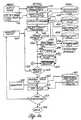
- FIG. 1a is a block diagram showing interconnections ofa data processing method and data files of the presentinvention;
- FIG. 1b is a block diagram of spreadsheet displaysgenerated by the present invention;
- FIGs. 2a, 2b, and 2c are graphs of capacitance versusinterline spacing;
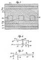
- FIG. 3 is a cross section view of a three-linestripline-type multilevel VLSI interconnect;
- FIG. 4 is a schematic diagram showing resistance,capacitance, and inductance relationships of the materialsshown in FIG. 3; and
- FIG. 5 is a schematic diagram of an exemplary striplineinterconnect.
- Embodiments of the present invention integrates four sets of dataprocessing methods to enable fast computer aided design ofcomplex three-dimensional interconnect structures. Ingeneral, the data processing methods receive input oflayout parameters and technology parameters identifying thecircuit to be designed, and generate output data files forthe SPICE circuit simulator. The four data processingmethods include (a) a batch-mode computation processingmethod that combines a 2-D/3-D finite difference numericalsimulation and a fast interpolation algorithm; (b) aninteractive design processing method with performancebrowsing, goal-directed synthesis, and on-line performanceevaluation; (c) an interactive SPICE subcircuit generatorand simulator; and (d) a spreadsheet-style graphical userinterface.
- The invention thus assists users in selectinginterconnect technologies for design-for-performance goalsand also in optimizing interconnect performance designs fordifferent types of chip packaging. By changing parametersand constants entered into the spreadsheets provided by theinvention, designers can customize the operation of theinvention for other variables such as reliability, thermaleffects, and cost effects.
- The batch mode element of the invention can beimplemented by programming a general purpose data processorusing standard equations in any suitable programminglanguage. The inventors have implemented this element inthe C programming language. The spreadsheet elements ofthe invention can be implemented using any of severalcommercially available spreadsheet computer programs. The inventors have implemented these elements using thecommercially available WINGZ spreadsheet running undercontrol of the UNIX operating system on a Hewlett-Packardworkstation.
- FIG. 1 shows main operational modes, process elements,and data files of the invention. The invention operates inthree modes, batch mode 100,
analysis mode 200, anddesign/simulation mode 300. In FIG. 1, process stepscorresponding to each of the three modes are labeled withreference numerals corresponding to the reference numeralused for each mode. - Operation of the invention can begin either in thebatch mode 100 or the
analysis mode 200. The batch mode100 is used to prepare data files for a new VLSIchip/MCM/PCB construction technique, and therefore is usedless frequently. Ordinarily a chip designer uses existingconstruction techniques and begins withanalysis mode 200.Each mode is discussed below. - Batch mode 100 comprises
steps - Initially, the program receives VLSI chip manufacturingprocess parameters entered 110 by a user andstored in
technology parameter file 400. Then the programcalls a numerical method-basedcapacitance simulator 112repeatedly for a plurality of interconnect configurationswith two widths and a range of inter-line spacings. Theresultingnumerical capacitance database 402 is called CapFile. In one preferred embodiment of the invention,thirty-three interconnect configurations, listed in Table1, are embedded in the capacitance simulator ("CapSim")program 112.Interconnect Configurations 1. M1 lines above Poly under M2 2. M1 lines above Substrate under M2 3. M1 lines above Silicide under M2 4. M1 lines above Poly under M3 5. M1 lines above Substrate under M3 6. M1 lines above Silicide under M3 7. M1 lines above Poly 8. M1 lines above Substrate 9. M1 lines above Silicide 10. M2 lines above sparse Ml and Poly 11. M2 lines above sparse M1 and Substrate 12. M2 lines above M1 13. M2 lines above sparse M1 and Poly under M3 14. M2 lines above sparse M1 and Substrate under M3 15. M2 lines above M1 under M3 16. M2 lines above Poly under M3 17. M2 lines above Substrate under M3 18. M2 lines above Silicide under M3 19. M2 lines above Poly 20. M2 lines above Substrate 21. M2 lines above Silicide 22. M3 lines above sparse M1 and Poly 23. M3 lines above sparse M1 and Substrate 24. M3 lines above sparse M2 25. M3 lines above M1 26. M3 lines above M2 27. M3 lines above Poly 28. M3 lines above Substrate 29. M3 lines above Silicide 30. Poly lines above Substrate under M1 31. Poly lines above Substrate under M2 32. Poly lines above Substrate under M3 33. Poly lines above Substrate - One of ordinary skill in the art will recognize theabbreviations in the above table as "M1" for metal 1, "M2"for
metal 2, "M3" for metal 3, and "poly" for polysilicon.The above interconnect configurations are for planarizedSMI technologies that have three metals and onepolysilicon. One of skill in the art will recognize thatthe twenty configurations can be extended for future SMItechnologies having more than three metal levels. - CapFile consists of tables representing two linewidths for each of the configurations shown in Table 1.The configurations of FIG. 1 apply to integrated circuits;other models are used for PCB/MCM. Each table comprisesone row for each configuration. Each row corresponds to aninterline spacing in microns. A typical table has rows forspacings of 0 microns to 15 microns in 1 micron increments.Each row comprises columns for the interline spacing inmicrons, the RC constant in ns per cm, total capacitance(Ct), interline, capacitance (Ci), ground capacitancebetween two lines (Cg12), ground capacitance from one lineto substrate (Cg1p) and a constant F (2Ci/Ct). Someconfigurations do not have Cg2 for lack of an upper metal,e.g., configurations 5 and 6. Substrate is considered asa conductor, so Cg1 always exists. Computation of tablevalues is described below.
- Each row of the CapFile tables is computed using acurve fitting method shown in
block 212. The method hasbeen implemented in a C language computer program calledCurveFit, which uses the least-square method known in theart to model the capacitance changes between minimumspacing (0 microns) and 15 µm. Polynomials of degree sixare used to curve-fit the non-linear relationship so thatthe maximum interpolation error can be within 5%. Cubicspline interpolation also can be used for curve-fitting.The CurveFit program also reads aresistance file 404 whichcontains the sheet rho data for polysilicon, metal 1,metal 2, and metal 3. The result of CurveFit is anequation file 406 containing curve-fit and linear-fit files, respectivelyshown in Table 2 and Table 3, with equations for Ci, Cg1, Cg2,and Rw arranged in SPICE format.

- If the inter-line spacing is narrower than 15 µm,curve-fit files are used. If the inter-line spacing iswider than 15 µm, linear-fit files are used. Since eachconfiguration in Table 1 has one curve-fit file and onelinear-fit file, the resulting
equation file 406 preferablyhas sixty-six such files. High-density VLSI designers mayuse curve-fit files most of the time since Cl, Cg1, and Cg2 donot change much after the spacing is wider than 15 µm. - Since several VLSI technologies use multipleconductors with different thickness and multiple insulatorswith different dielectric constants, those of skill in the art prefer numerical method-based capacitance simulatorsfor accurate modeling of VLSI interconnect capacitance.Empirically derived equations having multiple parameters,such as line width, inter-line spacing, conductor thicknessand dielectric thickness are known in the art forinterconnect modeling. Such equations cannot cover VLSIchip layout configurations with multiple dielectrics andvarious metal thickness. Furthermore, the ranges of linewidth and inter-line spacing that can be applied to themulti-parameter equations are limited.
- FIG. 3 is a schematic cross section of an exemplaryVLSI chip section 30 constructed with Metal 1 arrays undera
Metal 2 plane above Substrate. A low-temperature oxidelayer 36 (TEOS, εr=4.1) exists between metal 2 (referencenumeral 34) and a plurality of conductor lines 38a, 38b,38c comprising metal 1. Insulators between metal 1 andsubstrate 40 include phosilicate glass 44 (PSG, εr=4.0) andfield oxide 46 (FOX, εr=3.9). Aninsulation layer 32 coversthemetal layer 34. Three capacitance relationships existrelated to the center metal 1 line 38b. Two groundcapacitances (Cg1 and Cg2) are developed between line 38b andmetal 2 and the substrate, respectively. A one-sidedinter-metal-1-line capacitance (Ci) is developed betweenline 38b and either of lines 38a, 38c. If there is nometal 2 (34) above the metal lines 38a, 38b, 38c, then noground capacitance exists. - The relation of the three capacitance components andthe commonly used total capacitance (Ct) is expressed inEquation 1:
- The units of Ci, Cg1, and Cg2 are farads per micron(F/µm). In the known art, Ct is calculated and thensectioned for distributed single-line R,C circuit simulation. It is valid when the two adjacent lines 38b,38c remain in a quiet state. Due to electrical coupling inhigh-density interconnects, non-switching and longinterconnect lines adjacent to an active line often are notquiet. The effective RC-delay, and cross-talk must besimulated with distributed multi-line R,C models. On theother hand, interconnects on different levels are requiredby design to run in perpendicular directions, so thecoupling between different levels is small. Non-activeconductor levels, e.g., power supplies, are considered asquiet.
- A particular chip technology for VLSI design isaffected by three layout parameters (line width, linelength, and inter-line spacing of an interconnect line),and technology parameters (such as conductor thickness,dielectric thickness, dielectric constants, and tolerancevalues). The layout parameters are user-adjustable but thetechnology parameters are fixed and cannot be changed bydesigners. During VLSI layout, the values of Ci, Cg1, and Cg2are affected by the three layout parameters. The inter-linespacing affects the capacitance in a non-linearmanner. FIG. 2a contains a
graph 2 showing the non-linearrelationship of interline spacing to capacitance. Linewidth is fixed at .9 microns and the construction is M1arrays above substrate.Vertical scale 4 indicates faradsper micron. Horizontal scale 6 indicates interline spacingfrom 1 to 5 microns. Line 8 represents total capacitance,line 10 indicates interline capacitance, line 12 is groundcapacitance, andline 14 roughly indicates crosstalk noise.FIG. 2c illustrates the non-linear capacitance relationshipversus spacing, when metal 1 line width is fixed at 0.8 µmwhile the spacing is changed from 1.0 µm to 15 µm.Line 20represents interline Ci,line 22 represents Cg1, andline 24represents Cg2. The same phenomena can be found in otherconductor levels such as polysilicon,metal 2, and metal 3. - Since capacitance is non-linear in relation to inter-linespacing but linear in relation to line width and linelength, polynomials can be used to model capacitance as afunction of inter-line spacing, as shown below:

- The cwidth(s) is capacitance per unit length simulatedwith a fixed line width and s is a variable representingthe inter-line spacing. A least-square method known in theart can be used to curve-fit the non-linearity and generatecoefficients for the above polynomial of degree six. Thethree capacitance curves, Ci, Cg1, Cg2 in FIG. 2c, are modeledas three polynomials: Cimin(s) , Cg1min(s), and Cg2min(s), where minstands for the minimum width specified by the design rule.A reasonably wide width of 10 µm is chosen for polysilicon,metal 1, and
metal 2; 20 µm is chosen for metal 3. Thecoefficients of the six polynomials are embedded in aSPICE-format file shown in Tables 2 and 3. - Interconnect line width affects capacitance of a linein a linear manner, so the capacitances can be modeled inthe form of the following three equations:
- In these equations, widmin is the minimum width andwidmax is the reasonably wide width; w(in µm) is the linewidth variable. The Ci(w,s), Cg1(w,s) and Cg2(w,s) above areto be multiplied by the length parameter inside the SPICEsubcircuits. In this way, interconnect capacitances are parameterized with layout parameters for a selectedtechnology.
- Changes in line resistance are linearly proportionalto the temperature, the line length, and the inverse of theline width, so the resistance per unit length can becalculated by:
- Since Ci, Cg1, Cg2, and Rw can be polynomial-fitted asfunctions of interconnect dimension, their distributed R,Ceffects are modeled by a three-line π3 R,C circuit modelknown in the art, and consists of three cascaded π R,Cmodels to represent a distributed single-line interconnectfor circuit simulation. Considering the increased couplingamong submicron interconnects, we extend the single-line π3model to a three-line π3 model for accurate SMI RC-delayand cross-talk simulation.
- The electrical characteristics of VLSI interconnectsare simulated using SPICE by creating a SPICE subcircuitrepresentation of each interconnect. FIG. 4 is a schematicrepresentation of electrical characteristics of two linesof the interconnect of FIG. 3. The
interconnect 50 of FIG.4 has two input points 52, 54 which correspond to terminalsof lines 38b, 38c of FIG. 3. Each line 38b, 38c has an impedance represented respectively byresistors inductors 60.Capacitor 62 interconnects the lines and representsthe interline capacitance of FIG. 3. Ground capacitancesare respectively represented bycapacitors - A SPICE subcircuit call statement specifying twolines, 1.0-cm-long metal 1 arrays, line width of 4 µm andinter-line spacing of 2 µm would appear as follows:
X1 %in1 %in %in2 %out1 %out %out2 0 m1m2sb (4u 2u 1000u)
where X1 is the name of the metal 1 arrays to be modeled.A three-line model requires seven external node namesspecified to connect the three inputs, three outputs, andground to adjacent circuits. After the node namespecification, the above call statement specifies thesubcircuit being called, m1m2sb, and the three layoutparameters, width, spacing, and length (inside theparentheses). "m1m2sb" is the acronym for "Metal 1 arraysunderMetal 2 above Substrate." For 2.0-cm-long metal 1arrays, the specification is:
X2 %in1 %in %in2 %out1 %out %out2 0 m1m2sb (4u 2u 20000u) - The following specification will give betteraccuracy, however, because the number of sections isincreased from three to six:
X21 %in1 %in %in2 %tmp1 %tmp %tmp2 0 mim2sb (4u 2u 10000u)
X22 %tmp1 %tmp %tmp2 %out1 %out %out2 0 mim2sb (4u 2u 10000u) - With more sections, the total number of nodes to beprocessed by SPICE will be increased and the execution timewill be longer. For on-chip transmission line modeling,the length of each subcircuit call statement should bedetermined by the rise time.
- The batch-mode computation algorithm is derived fromthe "HIVE" algorithm as disclosed in the following papers: (1) K-J Changet al., "HIVE: An Express and AccurateInterconnect Capacitance Extractor For Submicro MultilevelConductor Systems," presented at the VMIC Conference, 11-12June 1991; (2) K-J Changet al., "HIVE: An EfficientInterconnect Capacitance Extractor to Support SubmicronMultilevel Interconnect Designs," presented at ICCAD,November 1991; and (3) S-Y Ohet al., "Physical andTechnological Limitations and Their Optimization inSubmicron ULSI Interconnect," presented at the ICVC '91conference, Seoul, Korea.
- The HIVE algorithm computes selective lateral andvertical capacitances of sub-micron IC interconnects usingfinite-difference methods. The non-calculated capacitancescan then be obtained through fast interpolation. Theassumptions which are used for extracting submicron on-chipinterconnect capacitances as reported in the above papersare also valid for MCM and PCB. These assumptions includethe following. First, interline ("Cil") and vertical("Cg") capacitances linearly vary with trace width when theinterline spacing is fixed. Second, with enough points fornumerical simulation of capacitances in which interlinespacing is varying and width fixed, other capacitances forany spacings bounded by the simulated spacings can beinterpolated. Capacitance values can be computed using theFCAP2 and FCAP3 algorithms which are known in the art andavailable in commercial C language libraries for numericalsimulation; these algorithms are described in the followingreferences: Kit Chamet al., Computer-Aided Design and VLSIDevice Development (2nd Edition), Lower AcademicPublishers, Norwell, Massachusetts, 1988, pp. 348-351, andKen Lee, "Three-Dimensional Modeling of InterconnectCapacitance and Inductance",Workshop on InterconnectModeling and Technology, IEEE Solid-State Circuits &Technology Committee, San Diego, California, May 1989.
- For example, the changes of both "Cil" and "Cg" of astripline for a thin-film MCM behave linearly when thewidth is changed but the spacing is fixed. Therefore, fora fixed spacing, only two capacitances need be calculatedusing numerical simulation; capacitance values fordifferent widths can be interpolated. However, due to theslight non-linearity of capacitance curves versus spacingwhen the width is fixed as shown in FIG. 2c, more pointsare needed using numerical simulation. This permits use oflinear, polynomial, or cubic spline interpolation fordifferent spacings depending on the accuracy desired. Ineither way, the interpolated capacitances are carefullychecked to ensure that the maximal induced error is around3% of the capacitance.
- The
analysis mode 200 comprisessteps 
- FIG. 1b shows a compressed representation of a mainspreadsheet 500 of the invention. The main spreadsheet 500is divided into a user parameter worksheet 502, a
performance assumptions worksheet 520, and aconstructiondatabase worksheet 530. A separateconstruction setupworksheet 540 is coupled to theconstruction databaseworksheet 530. Each of the worksheets comprises aplurality of interrelated cells. As is known in the art,each cell can be programmed with a numeric formula so thata change to one cell results in rapid calculation andredisplay of related cells. One of skill in the art willrecognize that the cells and worksheets can be representedin a conventional computer memory or using a relationaldatabase system. Preferably the worksheets are stored ona conventional mass storage device, such as a hard diskdrive, to enable long-term storage of the data therein. - The user parameter worksheet 502 preferably comprisesa plurality of
rows 504 each havingcells rows 504. The first row accepts user entry of a line widthrange in microns, such as 10 microns, 20 microns, etc. Thesecond row accepts user entry of a line spacing range inmicrons, such as 40 microns, 50 microns, etc. The thirdline displays available metallization models which areabbreviated by acronyms known in the art, such as SM, BMO,SL, DSS, etc. Thus, using the user parameter worksheet, auser can enter preferred interconnect line width andspacing for use by other elements of the invention. - Preferably the
assumptions worksheet 520 has aplurality ofcells - Preferably the
construction worksheet 530 comprises aplurality ofspreadsheet cells construction worksheet 530 contains allparameters relating to one particular construction type.Each column identifies a parameter. Table 5 listspreferred data types and units for each column.Construction Worksheet Columns Column Data Type Units 1 construction type acronym 2 layers integer 3 dielectric constant 4 core microns 5 prepreg microns 6 outer layer metal microns 7 inner layer metal microns 8 metal resistivity ohms/meter 9 metal overplate thickness mils 10 mask dielectric constant 11 mask thickness microns 12 in database boolean y/n - Coupled to the
assumptions worksheet 520 is a separateperformance database worksheet 550. Preferably theperformance worksheet 550 comprises a plurality of rows,each having a plurality of column cells representingelectrical performance characteristics of a particularconstruction for a particular number of traces, tracewidth, and trace spacing. The performance worksheet isactivated by selecting the PERF BROWSE option, which causesthe data processor to load and display a performanceworksheet. Table 6 lists preferred data types for eachcolumn of a row, including units and spreadsheet formulasby which the column cells are computed, for a five-linemodel. As indicated, the performance worksheet containsperformance values computed according to all the otherentered data.Performance Worksheet Data Types Column Name Units or Formula 1 type text 2 layers integer 3 model type acronym 4 reserved 5 reserved 6 number of traces integer 7 trace width mils 8 trace spacing mile 9 effective impedance ohms 10 effective PD ps/inch 11 latB crosstalk mV/V 12 latF crosstalk mV/V 13 vertical crosstalk mV/V 14 coupling coefficient (Ze-Zo)(Ze+Zo) 15 resistivity ohms/meter 16 even impedance ohms 17 odd impedance ohms 18 PD even ps/inch 19 PD odd ps/inch 20 inductance 1-2 L12/qqrt(L11*L22) 21 inductance 1-3 L13/sqrt(L11*L33) 22 inductance 1-4 L14/sqrt(L11*L44) 23 inductance 1-5 L15/sqrt(L11*L55) 24 inductance 2-3 L23/sqrt(L22*L33) 25 inductance 2-4 L24/sqart(L22*L44) 26 inductance 2-5 L25/sqrt(L22*L55) 27 inductance 3-4 L34/sqrt(L33*L44) 28 inductance 3-5 L35/sqrt(L33*L55) 29 inductance 4-5 L45/sqrt(L44*L55) 30 capacitance 1-1 farads/meter 31 capacitance 2-2 farads/meter 32 capacitance 3-3 farads/meter 33 capacitance 4-4 farads/meter 34 capacitance 5-5 farads/meter 35 capacitance 1-2 farads/meter 36 capacitance 1-3 farads/meter 37 capacitance 1-4 farads/meter 38 capacitance 1-5 farads/meter 39 capacitance 2-3 farads/meter 40 capacitance 2-4 farads/meter 41 capacitance 2-5 farads/meter 42 capacitance 3-4 farads/meter 43 capacitance 3-5 farads/meter 44 capacitance 4-5 farads/meter 45 to 54 capacitance of each line to planes1 and 2 farads/meter 55 capacitance plane to plane farads/meter 56 to 70 capacitance of each line to substrate farads/meter 71 to 85 inductance of each line to each other line henries/meter - Thus, each interconnect construction is specified witha common set of characteristic parameters, such as numberof layers, dielectric constants, dielectric thicknesses, conductor type, soldermask or overcoat dielectric constantand thickness, outer layer and inner layer conductorthicknesses, and number of coupling traces. Sincedifferent interconnect domains have different sets ofcharacteristic parameters, in the preferred embodimentthree separate construction worksheets are maintained forIC, MCM thin film, and PCB/MCM thick film constructions.
- The performance worksheet contains representative datapoints for interconnect capacitances which are extractednumerically for all the conceivable models of a newconstruction in the batch mode. For example, a 4-layer MCMconstruction can have models such as stripline (SL), dualstripline (DSS), surface microstrip (SM), and buriedmicrostrip outer (BMO). A linear interpolation algorithmcan then be applied to generate any other points bounded bythe width/spacing ranges of the simulated points. Thesimulated capacitances are subsequently used to deriveinductances L and transmission line properties, includingZo, Ze, Zeff (odd, even effective mode impedances); Pdo, Pde,Pdeff (odd, even effective propagation delays); and VB, VF(backward, forward crosstalks) for all the interconnectmodels. The formulas used for these derivations are knownin the art and are discussed, for example, in the followingreferences: H. B. Bakoglu,Circuits, Interconnections, andPackaging for VLSI, Addison-Wesley, Reading, Massachusetts,1990; A. Feller etal., "Crosstalk and Reflections inHigh-Speed Digital Systems,"Proceedings of Fall JointComputer Conference, 1965; J. Buchanan,BiCMOS/CMOS SystemsDesign, McGraw-Hill, Inc., 1991.
- Goal-directed interconnect synthesis helps users tonarrow down possible interconnect designs quickly. The domain of search is all processes/technologies that havebeen simulated in the batch mode. The invention extractsa subset of designs that satisfy multiple performancegoals, such as impedance and noise margin, specified by theuser.
- The user can also look at the effect of changing tracewidth/spacing on any performance variable by using thegraphing facility of the invention discussed below. Thisis done by showing any performance variable versus tracewidth and/or trace spacing. An arbitrary number of graphscan be generated, so a user can simultaneously visualizetrade-offs for different trace width/spacing designs aswell as their impact on several performance variables.
- To accomplish goal-directed synthesis, the user selectsSYNTHESIS from the spreadsheet menu tree. The SYNTHESISSETUP option is selected, causing the data processor todisplay a setup window on the workstation. Preferably thesetup window is a spreadsheet worksheet comprising fivecolumns entitled PARAMETER, UNIT, RELATIONSHIP, MINIMUMVALUE, MAXIMUM VALUE, and INPUT. Preferably the worksheethas ten rows identified with names in the PARAMETER column.The rows represent model name, layers in the interconnect,trace width (mils), trace spacing (mils), impedance (Ohms),signal propagation delay (picoseconds/inch), noise margin(mV/V) , lateral crosstalk (mV/V), vertical crosstalk(mV/V), and coupling coefficient. The parenthesized unitidentifiers are depicted in the UNITS column. In theRELATIONSHIP column the data processor displays referencetext such as noise margin data. The worksheet accepts userentry in the MINIMUM VALUE and MAXIMUM VALUE columns.Synthesis setup is then complete.
- Next, the user selects the GOAL-DIRECTED SYNTHESISoption from the spreadsheet menu. In response, the data processor displays a window of performance data forconstructions meeting the criteria specified in the setupwindow. The displayed data is selected from the
performance data worksheet 550 by comparing values thereinwith MINIMUM VALUE and MAXIMUM VALUE entries provided bythe user. - An evaluation panel is provided for users to do stackupdesign. Stackup design involves assigning signal orreference planes to each layer of an interconnectconstruction. Once a user specifies layer assignment fora selected construction, the invention can determine layermodels for each layer. Furthermore, on-line performanceevaluation can be done for each signal layer given anarbitrary trace width and spacing within the interpolationrange.
- Evaluation is initiated by selecting the EVALUATIONSETUP spreadsheet option from the menu. In response, thedata processor displays a spreadsheet worksheet containinga plurality of layer rows, each row corresponding to alayer of the construction type under analysis. Theworksheet further includes a plurality of layer cells ineach row corresponding to different parameters whichcharacterize each layer. Preferably, the layer cellspermit entry of data for layer type (soldermask or activelayer), layer assignment (mask, signal, blank signal, orreference), and layer model (surface microstrip, stripline,etc.). When these values are entered, evaluation setup iscomplete.
- Next, the user selects MODEL EVALUATION. In response,the data processor computes and fills in data for each cellof the performance worksheet, identified above in Table 6.Thus, by choosing a specific signal layer from theevaluation worksheet, the user can generate and simulate SPICE subcircuits through the interactive SPICE setupworksheet and SPICE window and thereby evaluate performanceof different layers.
- If the test of step 216 is true, control is passed tostep 220 in which the invention will generate a SPICE deckor file for the interconnect being analyzed. Passage ofcontrol to step 220 is usually accomplished by the usermoving the mouse of the workstation to the SPICEspreadsheet menu option. In response, the data processordisplays two sub-options: SPICE SETUP and SPICE CREATE.
- When the user selects SPICE SETUP, the data processordisplays a SPICE SETUP spreadsheet worksheet. Theworksheet displays setup conditions for SPICE simulation ofcoupling of specified traces. Traces can be specified asactive or inactive, where active means connecting the inputof the trace to a pulse that has a user-specified risetime. The user can specify the termination of a trace byproviding a characteristic impedance in ohms or byspecifying open termination. Preferably a first area ofthe worksheet contains cells for input of a defaultcharacteristic impedance, and for rise time, pulse width,and period of active trace input signals. A second area ofthe SPICE SETUP worksheet contains a plurality of rows,each row corresponding to an interconnect trace. Eachtrace row comprises a plurality of cells to store datarepresenting the trace number, whether the trace is activeor inactive, input impedance, whether ground is present,names of input and output nodes connected by theinterconnect, and a characteristic termination impedance.Each cell is filled by the user with numeric data for useby the SPICE CREATE option.
- When the user selects SPICE CREATE, in
step 220, themethod of the invention causes a data processor to read theequation file 406 and generate parameterized three-line π3circuit models for distributed R,C circuit simulation. Theresulting SPICE deck is written to a parameterized modelfile 420. - To form the SPICE deck, Cg1, and Cg2 read from theequation file are added to form Cg. Then Cg, Ci, and Rw aremultiplied by the line length of the interconnect anddivided by three, respectively, to become three separatecircuit elements. The capacitances on the boundary must befurther divided by two. For each configuration in Table 1,a curve-fit R,C file and a linear-fit R,C file isgenerated. The resulting parameterized model library hasforty distributed R,C SPICE subcircuits. The parametersfor each subcircuit are line width, inter-line spacing, andline length. Chip operating temperature is also aparameter but it can be accessed in a global manner andneed not be specified in each subcircuit call statement.
- After creation of a SPICE deck, the user can activatethe SPICE program using a separate workstation window, andspecify the just-created SPICE deck as input. All knownand ordinary SPICE functions can be executed.
- Once the performance database is built, the user canuse the invention's performance browser and graphicscapability to look at different curves of interest. Toplot a graph, the user first moves the workstation cursorto any single cell in the performance worksheet. Then theuser selects the PERFORMANCE PLOT option from thespreadsheet menu. Four options called WIDTH, SPACING,WIDTH WITH SPACING CONTOUR, and SPACING WITH WIDTH CONTOUR are available to plot capacitance versus trace width ortrace spacing. The selected option generates a graph basedon the data in the previously selected cell. Graphs aregenerated using the public-domain XGRAPH program developedby U.C. Berkeley.
- FIG. 2b shows a
typical graph 630 of effectiveimpedance versus interline spacing which can be produced ina workstation window by the invention. Thevertical scale 632 shows effective impedance and the horizontal scale 634shows interline spacing in microns.Lines - The spreadsheet menu preferably includes a plurality ofdatabase function menu options. The DATABASE DELETEfunction enables deletion of data in a worksheet. TheDATABASE CHECK EXISTING MODELS function performs a searchof a worksheet and finds all models matching a chosenconstruction. For example, when the CHECK EXISTING MODELSoption is selected, after user entry of layer number,construction technique, and core thickness, the dataprocessor will search the construction database to locateconstruction models matching the selected criteria.
- The WINDOWS option enables the user to rapidly enter acurrently active window for the PERFORMANCE, SYNTHESIS,EVALUATION, or SPICE functions. The MENU option has twosub-options to return the user to a main menu and torestart the system of the invention.
- Table 7 below shows a parameterized SPICE circuitinterconnect specification for an exemplary clock tree.
Clock Tree Interconnect Spec X1 %c1 %cntr %c2 %11 %left %12 0 m2m1py ( 4u 2u 2500u) X2 %c1 %cntr %c2 %r1 %rite %r2 0 m2m3sb ( 4u 2u 2500u) X3 %l1 %left %12 %lui %lu %lu2 0 m2sb ( 2u 2u 2350u) X4 %l1 %left %12 %ld1 %ld %ld2 0 m2m1py ( 2u 2u 1250u) X5 %r1 %rite %r2 %ru1 %ru %ru2 0 m2m3sb ( 2u 2u 1259u) X6 %r1 %rite %r2 %rd1 %rd %rd2 0 m2m3m1 ( 2u 2u 1250u) X7 %lu1 %lu %lu2 %lur1 %lur %lur2 0 m2m1py (.8u 1u 1250u) X8 %lu1 %lu %lu2 %lul1 %lul %lul2 0 m2m1py (.8u 1u 1250u) X9 %ld1 %ld %ld2 %ldr1 %ldr %ldr2 0 m2m1py (.8u 1u 1250u) X10 %ld1 %ld %ld2 %ldl1 %ldl %ld12 0 m2m1py (.8u 1u 1250u) X11 %ru1 %ru %ru2 %rur1 %rur %rur2 0 m2m3m1 ( 1u 1u 1250u) X12 %ru1 %ru %ru2 %rur1 %rul %rul2 0 m2m3m1 ( 1u 1u 1250u) X13 %rd1 %rd %rd2 %rdr1 %rdr %rdr2 0 m2m3sb ( 1u 1u 1250u) X14 %rd1 %rd %rd2 %rdr1 %rdl %rd12 0 m2m3sb ( 1u 1u 1250u) - The clock signal is distributed from the center, %cntr,to the eight cells through fourteen
metal 2 interconnectsegments. Each segment is described by a parameterizedinterconnect subcircuit call statement starting with "X".The subcircuit names being called in each statement, e.g.,m2mlpy and m2m3sb, start with m2 because the active levelismetal 2. The seven interconnect segments X2, X5, X6,X11, X12, X13, and X14, are under dense metal 3power/ground buses. Therefore, the corresponding calledsubcircuits have m3 in the middle of their names. Theclock skew between nodes %lul and %rur is 0.5 nanosecond.After the trace widths of X11 to X14 are increased to 1.0µm, the clock skew is decreased to 0.2 nanosecond. If thisis still not tolerable. Each SPICE input adjustment takesless than ten seconds. If the interconnect is notparameterized, circuit designers must run time-consumingcapacitance simulators several times. Furthermore, manualconversion of the capacitance values into distributed R,CSPICE subcircuits is tedious and error prone. - A SPICE input representing a clock distribution in H-treeis arranged by using the parameterized subcircuits forclock-skew simulations. Table 8 provides a listing of theinterconnect portion of the H-tree of this example.
H-tree Interconnect Portion Spec X1 %c1 %cntr %c2 %l1 %left %12 0 m2m1p_wc ( 4u 1u 2500u) X2 %c1 %cntr %c2 %r1 %rite %r2 0 m2m3s_wc ( 4u 1u 2500u) X3 %l1 %left %12 %lu1 %lu %lu2 0 m2sub_wc ( 2u 1u 1250u) X4 %11 %left %12 %ld %ld2 0 m2m1p_wc ( 2u 1u 1250u) X5 %r1 %rite &r2 %ru1 %ru %ru2 0 m2m3s_wc ( 2u 1u 1250u) X6 %r1 %rite &r2 %rd1 %rd %rd2 0 m2m3m1_wc ( 2u 1u 1250u) X7 %lu1 %lu &lu2 %lur1 %lur &lur2 0 m2m1p_wc (.8u 1u 1250u) X8 %lu1 %lu &lu2 %lul1 %lul &lu12 0 m2m1p_wc (.8u 1u 1250u) X9 %ld1 %ld %ld2 %ldr1 &ldr %ldr2 0 m2m1p_wc (.8u 1u 1250u) Xa %ld1 %1d %ld2 %ldl1 %ldl %ldl2 0 m2m1p_wc (.8u 1u 1250u) Xb %ru1 &ru &ru2 %rur1 %rur %rur2 0 m2m3m1_wc ( 1u .8u 1250u) Xc &ru1 %lu %ru2 %rul1 %rul2 0 m2m3m1_wc (1u .8u 1250u) Xd &rd1 %rd &rd2 %rdr1 %rdr %rdr2 0 m2m3s_wc ( 1u .8u 1250u) Xe %rd1 %rd %rd2 %rdl1 %rdl %rd12 0 m2m3s_wc ( 1u .8u 1250u) - The clock signal is transmitted by
metal 2 from %cntrto the eight cells. The four cells on the right side areunder a dense distribution of metal 3 power/ground buses.Each segment of the H-tree is represented by a subcircuitstarting with X. Each subcircuit consists of three lines.The center line represents the clock line for worst-casedesign. So seven nodes are needed for each subcircuitrepresenting three inputs, three outputs and the groundnode. - At first, the trace width of Xb to Xe subcircuits is0.8 µm, the same as that of X7 to Xa. Since the metal 3affects the interconnect capacitance and it is primarily onthe right-hand size, it causes the symmetric H-tree to have0.5 nanosecond clock skew. This is done by comparing thedelay of %lul with that of %rur. When the trace width ofXb to Xe is increased to 1.0 µm, the skew is decreased to0.2 nanosecond. The SPICE input can be adjusted in thisway until the clock skew is tolerable. Each SPICE inputchange takes less than ten seconds. If the SPICE deck isnot parameterized, VLSI designers have to do 2-D/3-D simulations for times to come up with a new SPICE deck. Ittakes at least two hours to make one trace width changesince the 3-D capacitance simulation of each of the foursubcircuits needs at least fifteen minutes. Thearrangement of the new simulated capacitance into SPICEdeck is tedious and takes about an hour.
- A simplified chip-to-chip signal communicationoptimization problem demonstrates how the invention helpsdesigners analyze and optimize the interconnect design. Inthis example, shown in FIG. 5, a
signal 72 transmits froman output driver pad to a receiver pad 82 through amulti-linetransmission line 78, 80 on an MCM, ignoring solderbumps required between the chips and the MCM. To furthersimplify the example, theoutput driver signal 72 isrepresented by a single low-to-high pulse with 0.2 nsrisetime and 40 Ω source resistance. The receiver isassumed to have a high input impedance. The distancebetween driver and receiver is required to be 8 cm on aMCM. Interconnect choices include stripline or microstripcoupler configuration on several MCMs with differentdielectric thicknesses and with or without coatings. Thegoal is to achieve minimum delay and crosstalk possible andno more than 1 ns delay and 100 mV/V crosstalk. - To use the invention to optimize the design in thiscase, first, a user runs batch-mode simulations forpossible interconnect design configurations. Severalconstruction choices for the MCMs are reviewed from thelist in Table 1. Three are polyamide and ceramic materialswith dielectric constants of 4.0 and 9.0, respectively.Coatings of various thicknesses are available formicrostrips. Also, trace width ranges from 10 to 60 µm,and trace spacing ranges from 40 to 500 µm. The result of the batch-mode simulation is the interconnect R,L,C,impedance, propagation delay, and crosstalk information inthe database for surface microstrip, buried microstripouter (with coating), and stripline configurations forvarious technologies.
- Next the designer can enter impedance and noise margingoals in the synthesis worksheet and the invention willreturn all the choices that satisfy the requirements. Theuser can then use the evaluation worksheet to do moredetailed design by specifying layer assignments for thechosen MCM technology. Arbitrary choices of tracewidth/spacing, coupling length, and risetime can bespecified, and performance information can subsequently bederived.
- Thus, the invention helps designers to analyze andoptimize interconnect designs in an interactive way. Thereare other design constraints, such as cost, thermalmanagement, power consumption, and manufacturability, thatdetermine the final choice of a certain technology. Forthis application example, an open-ended termination couplerhas less power consumption than a well-terminated coupler.The cost of 9.0 dielectric material is less than that of4.0 dielectric material, and the cheaper material maysatisfy performance requirements as well. Microstrip withcoating is more manufacturable than strip-lines. It wouldbe difficult to know all the constraints up front beforeexploring possible alternatives. Since the example has adriver with 0.2 ns risetime and 40 Ω source resistance, anopen-ended termination microstrip (with coating) couplerwith length of 8 cm is used on a 4.0 dielectric materialwith T/W + 40 µm, T\S + 60 µm, and dielectric thickness of20 µm. For this choice, the final performance result are0.54 ns delay, and 31 and 61 mV/V reduced noise margin due to crosstalk and reflection for near and far ends,respectively.
- The invention database can also be used not only forpre-layout system-level cost-performance analysis but alsofor schematic capturing and post-layout parasitic circuitextraction. However, both the database format and thelayout extraction methods for the IC/MCM/PCB tools must bemodified before the interconnect performance extractionroutines and database can be integrated and used.
- Thus, this invention provides an interconnect modelingsystem with many significant advantages. Embodiments thereofimproves the productivity of VLSI designers throughefficient SPICE deck generations for interconnect designs.The invention allows VLSI designers to specify accurateinterconnect models as easy as transistor models withoutany 2-D/3-D simulations. Existing SPICE simulator softwareis used unmodified. The invention isolates the chipdesigner from the details of SMI geometry and processvariations. Errors which are commonly found during manualSPICE deck generations are reduced significantly.Submicron VLSI circuits can be easily optimized by usingthe non-linear multi-variable optimizer and SPICE sinceboth the transistors and the interconnects areparameterized.
- One of ordinary skill in the art will recognize thatthis invention could easily be used for interconnectmodeling of multi-chip modules, hybrid packaging, andprinted circuit boards. The invention provides immediateresults to the user and the average execution times of thethree functions in an HP/Apollo 720 workstation are within1 second while 2-D/3-D ad-hoc simulations take about 20-1000 seconds. Therefore, the time required for anembodiment of the invention to calculate tens to hundredsof data points for all the user-specified models for aconstruction is much less than the time needed for 2-D/3-Dad-hoc simulations, which provide a single data point fora specified geometry.
- Further technical background relating to the technologydisclosed herein may be found in the followingpublications:
- (a) Al Barberet al., "Modeling and Analysis of HighSpeed VLSI Interconnects for Digital Applications,"HP LabsReport HPL-02-03, January 1992.
- (b) L. Barfordet al., "Parametric Design Assistant andits Application to PCB Construction,"HP DTC, May 1991.
- (c) Kit Chamet al., "CMOS14/BiCMOS14 Process andPerformance,"Proceedings of HP DTC, pp. 429-436, May 1991.
- (d) W. H. Chang, "Analytical IC Metal-Line CapacitanceFormulas,"IEEE Trans. Microwave Theory and Technique, pp.608-611, Sep. 1976.
- (e) J. H. Chernet al., "Multilevel Metal CapacitanceModels for CAD Design Syntheses Systems,"IEEE ElectronDevice Letters, vol. EDL-33, pp.32-34, Jan 1992,
- (f) Informix Software, Inc.,Wingz Reference Manual,1991,
- (g) IPC,Design Guidelines for Electronic PackagingUtilizing High-speed Techniques, IPC-D-317 Report, AmericanNational Standards Institute, 1991.
- (h) N.P. van der Meijset al., "An Efficient FiniteElement Method for Submicron IC Capacitance Extraction,"26th ACM/IEEE Design Automation Conference, pp. 678-681,June 1989.
- (i) Larry L. Moresco, "Electronic System Packaging:The Search for Manufacturing the Optimum in a Sea ofConstraints,"IEEE Trans. Comp., Hybrids, Manuf. Technol.,vol. 11, pp. 494-508, September 1990.
- (j) Olgierd A. Palusinskiet al., "Modeling ofPerformance-Related Design Trade-offs in Multiple-ChipAssemblies,"Proceedings of IEEE/CHMT IEMT Symposium, pp.333-336, March 1991.
- (k) Vivek Raghavanet al., "A New Nonlinear DriverModel for Interconnect Analysis,"28th ACM/IEEE DesignAutomation Conference, pp. 561-566, June 1991.
- (l) T. Sakuraiet al., "Simple Formulas for Two- andThree-Dimensional Capacitances,"IEEE Trans. ElectronDevices, pp. 183-185, Feb 1983.
- (m) Peter A. Sandborn, "A Software Tool for TechnologyTrade-off Evaluation in Multichip Packaging,"IEEE/CHMTIEMT Symposium, pp. 337-340, 1991,
- (n) TMA, Inc.,TMA Raphael User's Manual, Oct. 1991.
- (o) Rick Walker etal., "Circuit Optimization Using theSimplex Algorithm,"Proceedings of HP DTC, pp. 390-397, May1989.


Claims (10)
- A computer-aided method of designing semiconductorinterconnects, the method comprising the steps of:selecting a semiconductor interconnect configuration;operating (200) a general purpose data processor todisplay a first spreadsheet (502) of semiconductor constructionparameters for the selected interconnect configuration andselecting specific interconnect line parameters therefrom;accessing a stored database (402, 404, 408) to readelectrical characteristics of the selected interconnectconfiguration;operating the data processor to display a secondspreadsheet (520) of electrical parameter data for the selectedinterconnect configuration based on said characteristics readfrom the stored database, and selecting specific electricalparameters therefrom;providing (222) the data processor with desired electricalperformance goal data such as impedance and noise margin andoperating the data processor to perform goal directedsynthesis and to display a third spreadsheet (530) ofconstruction data matching the goal data;wherein each of the spreadsheets comprises a plurality ofautomatically updated spreadsheet cells (506, 524, 534)organised in a matrix or rows (504) and columns.
- A method as in claim 1 wherein the step of providing(222) the data processor with desired electrical performancegoal; data comprises:providing maximum and minimum goal values for at least oneparameter chosen from the group of trace width, trace spacing, impedance, signal propagation delay, noise margin,and crosstalk, andoperating the data processor to display the goal valuesin a synthesis setup worksheet that has a plurality ofsynthesis cells organised in a matrix of rows and columns.
- A method as in claim 1 wherein each row of thethird spreadsheet relates to a single construction type andeach column of the first worksheet contains parameter datarepresenting a unique physical characteristic of theselected configuration.
- A method as in claim 1 and further comprising thesteps of:operating the data processor to display and receivedata in an evaluation setup worksheet having a plurality ofrows each corresponding with a layer of the selectedconfiguration, andspecifing a layer assignment for each said layer.
- A method as in claim 1 and further comprising thestep of operating (220) the data processor to write a fileof SPICE subcircuit data corresponding to the selectedconfiguration.
- A method as in claim 5 and further comprising thestep of operating the data processor to display and receivedata in a SPICE setup worksheet having a plurality of rowseach corresponding with a trace of the selectedconfiguration and a plurality of columns for entry ofdriving signal data and characteristic impedance of eachrow.
- A method as in claim 1 wherein the step ofaccessing the stored database comprises interpolatingelectrical performance data for performance characteristicsnot present in the stored database.
- A method as in claim 7 wherein interpolatingelectrical performance data comprises:reading a plurality of material configuration valuescorresponding with a plurality of semiconductor trace linewidth values from a capacitance data file (402); anditeratively computing, for a plurality of trace linewidths of the selected configuration, electricalperformance characteristics of said selected configuration,said electrical performance characteristics includingan interline capacitance value and a ground capacitancevalue.
- A method as in claim 8 wherein the materialconfiguration values comprise (a) total capacitance and (b)data corresponding to at least two layout parametersrelating to the selected configuration, the layoutparameters selected from the set of line width, line lengthand interline spacing.
- A method as in claim 7 wherein interpolatingelectrical performance data comprises:reading a database table containing capacitance valuesfor a multiple-trace interconnect, andsetting one of the electrical performancecharacteristics of the selected configuration equal toa capacitance value of said multiple-trace interconnect.
Applications Claiming Priority (3)
| Application Number | Priority Date | Filing Date | Title |
|---|---|---|---|
| US89210292A | 1992-06-02 | 1992-06-02 | |
| US892102 | 1992-06-02 | ||
| PCT/US1993/005186WO1993024896A1 (en) | 1992-06-02 | 1993-06-01 | Computer-aided design methods and apparatus for multilevel interconnect technologies |
Publications (2)
| Publication Number | Publication Date |
|---|---|
| EP0597087A1 EP0597087A1 (en) | 1994-05-18 |
| EP0597087B1true EP0597087B1 (en) | 1999-07-28 |
Family
ID=25399373
Family Applications (1)
| Application Number | Title | Priority Date | Filing Date |
|---|---|---|---|
| EP93914287AExpired - LifetimeEP0597087B1 (en) | 1992-06-02 | 1993-06-01 | Computer-aided design method for multilevel interconnect technologies |
Country Status (5)
| Country | Link |
|---|---|
| US (1) | US5610833A (en) |
| EP (1) | EP0597087B1 (en) |
| JP (1) | JPH07501906A (en) |
| DE (1) | DE69325770T2 (en) |
| WO (1) | WO1993024896A1 (en) |
Families Citing this family (126)
| Publication number | Priority date | Publication date | Assignee | Title |
|---|---|---|---|---|
| JPH0897215A (en)* | 1994-09-29 | 1996-04-12 | Sony Corp | Simulation method of electric characteristic of semiconductor device and input data forming equipment for the simulation method |
| US5903469A (en)* | 1994-11-08 | 1999-05-11 | Synopsys, Inc. | Method of extracting layout parasitics for nets of an integrated circuit using a connectivity-based approach |
| US5893123A (en)* | 1995-06-22 | 1999-04-06 | Tuinenga; Paul W. | System and method of integrating a spreadsheet and external program having output data calculated automatically in response to input data from the spreadsheet |
| US5812983A (en)* | 1995-08-03 | 1998-09-22 | Kumagai; Yasuo | Computed medical file and chart system |
| KR0182006B1 (en)* | 1995-11-10 | 1999-04-15 | 김광호 | Method for calculating parasitic capacitance caused by semiconductor package device and molding material |
| US6035300A (en)* | 1995-12-15 | 2000-03-07 | International Business Machines Corporation | Method and apparatus for generating a user interface from the entity/attribute/relationship model of a database |
| US6374203B1 (en)* | 1996-02-05 | 2002-04-16 | Motorola, Inc. | Method of modeling circuit cells with distributed serial loads |
| US5715408A (en)* | 1996-04-19 | 1998-02-03 | Cadence Design System, Inc. | Interconnect termination for high speed circuits |
| JP2918101B2 (en)* | 1996-07-25 | 1999-07-12 | 日本電気株式会社 | Layout method of semiconductor integrated circuit |
| US6202195B1 (en)* | 1996-07-26 | 2001-03-13 | Matsushita Electric Industrial Co., Ltd. | Semiconductor integrated circuit layout method |
| US5757655A (en)* | 1996-08-26 | 1998-05-26 | Micron Technology, Inc. | Method and system for producing dynamic property forms and compacting property databases |
| US6349401B2 (en)* | 1996-09-12 | 2002-02-19 | Matsushita Electric Industrial Co., Ltd. | Semiconductor integrated circuit, design method and computer-readable medium using a permissive current ratio |
| US6086238A (en)* | 1996-10-07 | 2000-07-11 | International Business Machines Corporation | Method and system for shape processing within an integrated circuit layout for parasitic capacitance estimation |
| US5831870A (en)* | 1996-10-07 | 1998-11-03 | International Business Machines Corporation | Method and system for characterizing interconnect data within an integrated circuit for facilitating parasitic capacitance estimation |
| US5838582A (en)* | 1996-10-07 | 1998-11-17 | International Business Machines Corporation | Method and system for performing parasitic capacitance estimations on interconnect data within an integrated circuit |
| US5910899A (en)* | 1996-10-25 | 1999-06-08 | Advanced Micro Devices, Inc. | Method for performing floorplan timing analysis using multi-dimensional feedback in a spreadsheet with computed hyperlinks to physical layout graphics and integrated circuit made using same |
| US5896301A (en)* | 1996-10-25 | 1999-04-20 | Advanced Micro Devices, Inc. | Method for performing floorplan timing analysis using multi-dimensional feedback in a histogram and integrated circuit made using same |
| US5903472A (en)* | 1996-10-25 | 1999-05-11 | Advanced Micro Devices, Inc. | Method for performing floorplan timing analysis by selectively displaying signal paths based on slack time calculations and integrated circuit made using same |
| US6202043B1 (en)* | 1996-11-12 | 2001-03-13 | Invention Machine Corporation | Computer based system for imaging and analyzing a process system and indicating values of specific design changes |
| JP2954894B2 (en)* | 1996-12-13 | 1999-09-27 | 株式会社半導体理工学研究センター | Integrated circuit design method, database device for integrated circuit design, and integrated circuit design support device |
| US5923565A (en)* | 1997-01-02 | 1999-07-13 | Vlsi Technology, Inc. | Apparatus and method for extracting capacitance in the presence of two ground planes |
| US6708144B1 (en)* | 1997-01-27 | 2004-03-16 | Unisys Corporation | Spreadsheet driven I/O buffer synthesis process |
| US5946211A (en)* | 1997-02-28 | 1999-08-31 | The Whitaker Corporation | Method for manufacturing a circuit on a circuit substrate |
| US5923568A (en)* | 1997-03-31 | 1999-07-13 | Hewlett-Packard Company | Distributed capacitance estimations of interconnects within integrated circuits |
| JP2910723B2 (en)* | 1997-04-09 | 1999-06-23 | 日本電気株式会社 | Semiconductor integrated circuit design support method, system using the method, and recording medium storing the method |
| JPH10313058A (en)* | 1997-05-13 | 1998-11-24 | Toshiba Corp | Semiconductor integrated circuit design apparatus, semiconductor integrated circuit design method, computer-readable recording medium storing semiconductor integrated circuit design program, and semiconductor integrated circuit manufacturing method |
| US6023576A (en)* | 1997-08-04 | 2000-02-08 | Lucent Technologies Inc. | Fast transient circuit simulation of electronic circuits including a crystal |
| CN1114169C (en)* | 1997-09-02 | 2003-07-09 | 日立化成工业株式会社 | Method and system for approximating distributed constant line |
| US6018623A (en)* | 1997-10-10 | 2000-01-25 | Hewlett-Packard Company | Method and system for determining statistically based worst-case on-chip interconnect delay and crosstalk |
| US6000050A (en)* | 1997-10-23 | 1999-12-07 | Synopsys, Inc. | Method for minimizing ground bounce during DC parametric tests using boundary scan register |
| US6009257A (en)* | 1997-10-27 | 1999-12-28 | Ncr Corporation | Computer system and computer implemented method for generating, displaying and simulating a hierarchical model having cross-branch connections using multiplicity trees |
| US6128769A (en)* | 1997-12-31 | 2000-10-03 | Intel Corporation | Method for analyzing and efficiently reducing signal cross-talk noise |
| US6189131B1 (en)* | 1998-01-14 | 2001-02-13 | Lsi Logic Corporation | Method of selecting and synthesizing metal interconnect wires in integrated circuits |
| US6102960A (en)* | 1998-02-23 | 2000-08-15 | Synopsys, Inc. | Automatic behavioral model generation through physical component characterization and measurement |
| US6212665B1 (en) | 1998-03-27 | 2001-04-03 | Synopsys, Inc. | Efficient power analysis method for logic cells with many output switchings |
| US6188975B1 (en) | 1998-03-31 | 2001-02-13 | Synopsys, Inc. | Programmatic use of software debugging to redirect hardware related operations to a hardware simulator |
| US6192507B1 (en)* | 1998-05-27 | 2001-02-20 | International Business Machines Corporation | Method for generating an electrical circuit comprising dielectrics |
| JPH11353338A (en)* | 1998-06-04 | 1999-12-24 | Mitsubishi Electric Corp | Simulation method of integrated circuit and recording medium |
| US6137546A (en)* | 1998-07-20 | 2000-10-24 | Sony Corporation | Auto program feature for a television receiver |
| US6279142B1 (en)* | 1998-10-02 | 2001-08-21 | International Business Machines Corporation | Method of on-chip interconnect design |
| US6453276B1 (en)* | 1998-12-22 | 2002-09-17 | Unisys Corporation | Method and apparatus for efficiently generating test input for a logic simulator |
| US6330704B1 (en) | 1999-02-09 | 2001-12-11 | Coyote Systems, Inc. | Method and apparatus for three dimensional interconnect analysis |
| US6407576B1 (en)* | 1999-03-04 | 2002-06-18 | Altera Corporation | Interconnection and input/output resources for programmable logic integrated circuit devices |
| US7016794B2 (en) | 1999-03-16 | 2006-03-21 | Lsi Logic Corporation | Floor plan development electromigration and voltage drop analysis tool |
| US6675139B1 (en) | 1999-03-16 | 2004-01-06 | Lsi Logic Corporation | Floor plan-based power bus analysis and design tool for integrated circuits |
| US6327693B1 (en)* | 1999-04-08 | 2001-12-04 | Chung-Kuan Cheng | Interconnect delay driven placement and routing of an integrated circuit design |
| JP2000315221A (en)* | 1999-04-30 | 2000-11-14 | Matsushita Electric Ind Co Ltd | Integrated circuit device design database and integrated circuit device design method |
| JP4363716B2 (en)* | 1999-06-25 | 2009-11-11 | 株式会社東芝 | LSI wiring structure design method |
| US6381730B1 (en)* | 1999-07-09 | 2002-04-30 | Sequence Design, Inc. | Method and system for extraction of parasitic interconnect impedance including inductance |
| US6689634B1 (en)* | 1999-09-22 | 2004-02-10 | Texas Instruments Incorporated | Modeling technique for selectively depopulating electrical contacts from a foot print of a grid array (BGA or LGA) package to increase device reliability |
| US6590419B1 (en)* | 1999-10-12 | 2003-07-08 | Altera Toronto Co. | Heterogeneous interconnection architecture for programmable logic devices |
| US6510539B1 (en) | 1999-10-29 | 2003-01-21 | International Business Machines Corporation | System and method for physically modeling electronic modules wiring |
| US6665845B1 (en)* | 2000-02-25 | 2003-12-16 | Sun Microsystems, Inc. | System and method for topology based noise estimation of submicron integrated circuit designs |
| US6853999B1 (en)* | 2000-04-12 | 2005-02-08 | General Electric Company | Method and apparatus for designing lamps with different phosphor blends |
| US6340631B1 (en)* | 2000-05-31 | 2002-01-22 | Taiwan Semiconductor Manufacturing Company, Ltd | Method for laying out wide metal lines with embedded contacts/vias |
| US6618837B1 (en)* | 2000-09-14 | 2003-09-09 | Cadence Design Systems, Inc. | MOSFET modeling for IC design accurate for high frequencies |
| US6467069B2 (en)* | 2000-12-15 | 2002-10-15 | International Business Machines Corporation | Timing closure and noise avoidance in detailed routing |
| US6532576B1 (en) | 2001-03-07 | 2003-03-11 | Lsi Logic Corporation | Cell interconnect delay library for integrated circuit design |
| US6539527B2 (en) | 2001-03-19 | 2003-03-25 | Hewlett-Packard Company | System and method of determining the noise sensitivity of an integrated circuit |
| US6766499B1 (en) | 2001-04-05 | 2004-07-20 | Lsi Logic Corporation | Buffer cell insertion and electronic design automation |
| US6721614B2 (en)* | 2001-05-21 | 2004-04-13 | International Business Machines Corporation | Multi-discipline universal CAD library |
| US20020198696A1 (en)* | 2001-06-08 | 2002-12-26 | Hector Sanchez | Method and apparatus for designing and making an integrated circuit |
| JP4035354B2 (en)* | 2001-07-11 | 2008-01-23 | 富士通株式会社 | Electronic circuit design method and apparatus, computer program, and storage medium |
| US20030058604A1 (en)* | 2001-09-13 | 2003-03-27 | Canagasaby Karthisha S. | Method and apparatus to emulate external IO interconnection |
| US6956284B2 (en) | 2001-10-26 | 2005-10-18 | Staktek Group L.P. | Integrated circuit stacking system and method |
| US7485951B2 (en)* | 2001-10-26 | 2009-02-03 | Entorian Technologies, Lp | Modularized die stacking system and method |
| US20030234443A1 (en) | 2001-10-26 | 2003-12-25 | Staktek Group, L.P. | Low profile stacking system and method |
| US7656678B2 (en)* | 2001-10-26 | 2010-02-02 | Entorian Technologies, Lp | Stacked module systems |
| US6914324B2 (en)* | 2001-10-26 | 2005-07-05 | Staktek Group L.P. | Memory expansion and chip scale stacking system and method |
| US7026708B2 (en)* | 2001-10-26 | 2006-04-11 | Staktek Group L.P. | Low profile chip scale stacking system and method |
| US6940729B2 (en) | 2001-10-26 | 2005-09-06 | Staktek Group L.P. | Integrated circuit stacking system and method |
| US7310458B2 (en) | 2001-10-26 | 2007-12-18 | Staktek Group L.P. | Stacked module systems and methods |
| US20040195666A1 (en)* | 2001-10-26 | 2004-10-07 | Julian Partridge | Stacked module systems and methods |
| US20060255446A1 (en)* | 2001-10-26 | 2006-11-16 | Staktek Group, L.P. | Stacked modules and method |
| US7371609B2 (en)* | 2001-10-26 | 2008-05-13 | Staktek Group L.P. | Stacked module systems and methods |
| US6763503B1 (en)* | 2001-11-20 | 2004-07-13 | Sun Microsystems, Inc. | Accurate wire load model |
| US7620525B2 (en)* | 2001-11-28 | 2009-11-17 | Smc Corporation Of America | Method of generating CAD files and delivering CAD files to customers |
| US6934922B1 (en)* | 2002-02-27 | 2005-08-23 | Xilinx, Inc. | Timing performance analysis |
| US20030182640A1 (en)* | 2002-03-20 | 2003-09-25 | Alani Alaa F. | Signal integrity analysis system |
| US6658629B1 (en)* | 2002-05-09 | 2003-12-02 | Sun Microsystems, Inc. | Technique for optimizing decoupling capacitance subject to leakage power constraints |
| US6931613B2 (en) | 2002-06-24 | 2005-08-16 | Thomas H. Kauth | Hierarchical feature extraction for electrical interaction calculations |
| US6898545B2 (en) | 2002-06-28 | 2005-05-24 | Agilent Technologies Inc | Semiconductor test data analysis system |
| US6810505B2 (en)* | 2002-07-10 | 2004-10-26 | Lsi Logic Corporation | Integrated circuit design flow with capacitive margin |
| WO2004061724A1 (en)* | 2002-12-17 | 2004-07-22 | International Business Machines Corporation | Asic clock floor planning method and structure |
| US6938230B2 (en)* | 2003-02-19 | 2005-08-30 | Hewlett-Packard Development Company, L.P. | System and method for evaluating signal trace discontinuities in a package design |
| US7542304B2 (en) | 2003-09-15 | 2009-06-02 | Entorian Technologies, Lp | Memory expansion and integrated circuit stacking system and method |
| US7093206B2 (en)* | 2003-10-21 | 2006-08-15 | International Business Machines Corp. | Computer aided design method and apparatus for modeling and analyzing on-chip interconnect structures |
| US7088121B1 (en) | 2003-11-17 | 2006-08-08 | Siprosys, Inc. | Non-contact method and apparatus for on-line interconnect characterization in VLSI circuits |
| US7219322B2 (en)* | 2004-04-27 | 2007-05-15 | Hewlett-Packard Development Company, L.P. | Multiple propagation speeds of signals in layered circuit apparatus |
| US20050251769A1 (en)* | 2004-05-04 | 2005-11-10 | Frank Mark D | System and method for determining signal coupling in a circuit design |
| US20050249479A1 (en)* | 2004-05-04 | 2005-11-10 | Frank Mark D | System and method for determining signal coupling coefficients for vias |
| US7137088B2 (en) | 2004-05-04 | 2006-11-14 | Hewlett-Packard Development Company, L.P. | System and method for determining signal coupling coefficients for lines |
| US20050251774A1 (en)* | 2004-05-07 | 2005-11-10 | Shah Gaurav R | Circuit design property storage and manipulation |
| JP2005339003A (en)* | 2004-05-25 | 2005-12-08 | Matsushita Electric Ind Co Ltd | Circuit analysis method and circuit analysis apparatus |
| TW200540611A (en)* | 2004-06-04 | 2005-12-16 | Hon Hai Prec Ind Co Ltd | System and method for verifying delay of a motherboard layout |
| US7143389B2 (en)* | 2004-07-28 | 2006-11-28 | Hewlett-Packard Development Company, L.P. | Systems and methods for generating node level bypass capacitor models |
| US20060043558A1 (en)* | 2004-09-01 | 2006-03-02 | Staktek Group L.P. | Stacked integrated circuit cascade signaling system and method |
| US20060076547A1 (en)* | 2004-09-24 | 2006-04-13 | Mentor Graphics Corp. | Three-dimensional viewing and editing of microcircuit design |
| US7334209B1 (en)* | 2004-10-15 | 2008-02-19 | Xilinx, Inc. | Method and system for generating multiple implementation views of an IC design |
| US7284227B1 (en) | 2004-10-15 | 2007-10-16 | Xilinx, Inc. | Method and system for generating implementation files from a high level specification |
| US7299445B2 (en) | 2004-10-29 | 2007-11-20 | Synopsys, Inc. | Nonlinear receiver model for gate-level delay calculation |
| US20060175693A1 (en)* | 2005-02-04 | 2006-08-10 | Staktek Group, L.P. | Systems, methods, and apparatus for generating ball-out matrix configuration output for a flex circuit |
| US7033861B1 (en)* | 2005-05-18 | 2006-04-25 | Staktek Group L.P. | Stacked module systems and method |
| US7774725B1 (en) | 2005-11-04 | 2010-08-10 | Purdue Research Foundation | Computationally efficient modeling and simulation of large scale systems |
| US7978206B2 (en)* | 2005-11-28 | 2011-07-12 | Autodesk, Inc. | Look-up table action |
| US7860691B2 (en)* | 2005-11-28 | 2010-12-28 | Autodesk, Inc. | Dynamic blocks |
| US7999827B2 (en)* | 2005-11-28 | 2011-08-16 | Autodesk, Inc. | Method and system for generating dynamic blocks |
| JP2007213269A (en)* | 2006-02-08 | 2007-08-23 | Toshiba Corp | Stress analysis method, wiring structure design method, program, and semiconductor device manufacturing method |
| US7712068B2 (en)* | 2006-02-17 | 2010-05-04 | Zhuoxiang Ren | Computation of electrical properties of an IC layout |
| US8015510B2 (en)* | 2006-02-17 | 2011-09-06 | Mentor Graphics Corporation | Interconnection modeling for semiconductor fabrication process effects |
| WO2007100558A2 (en)* | 2006-02-17 | 2007-09-07 | Mentor Graphics Corporation | Modeling for semiconductor fabrication process effects |
| US8381164B2 (en)* | 2006-03-28 | 2013-02-19 | The Boeing Company | Method and system of intelligent interactive graphics electrical plug map to analyze text and distances between electrical contacts and physical layout file builder |
| US7490304B2 (en)* | 2006-06-23 | 2009-02-10 | International Business Machines Corporation | Determining geometrical configuration of interconnect structure |
| US7417310B2 (en) | 2006-11-02 | 2008-08-26 | Entorian Technologies, Lp | Circuit module having force resistant construction |
| US7770141B2 (en)* | 2007-01-29 | 2010-08-03 | United Microelectronics Corp. | Computer recording medium for storing program of checking design rule of layout |
| US8053349B2 (en)* | 2007-11-01 | 2011-11-08 | Texas Instruments Incorporated | BGA package with traces for plating pads under the chip |
| US7665057B2 (en)* | 2008-02-13 | 2010-02-16 | Inventec Corporation | Method for calculating optimal length of trace between adjoining bends and computer accessible storage media |
| US9207294B1 (en)* | 2011-01-30 | 2015-12-08 | Sven Simon | Method and apparatus for the contactless determination of electrical quantities |
| US9984029B2 (en)* | 2014-04-18 | 2018-05-29 | Qualcomm Incorporated | Variable interconnect pitch for improved performance |
| US9361418B2 (en) | 2014-06-23 | 2016-06-07 | Synopsys, Inc. | Nanowire or 2D material strips interconnects in an integrated circuit cell |
| US9378320B2 (en) | 2014-06-23 | 2016-06-28 | Synopsys, Inc. | Array with intercell conductors including nanowires or 2D material strips |
| US10037397B2 (en) | 2014-06-23 | 2018-07-31 | Synopsys, Inc. | Memory cell including vertical transistors and horizontal nanowire bit lines |
| US9400862B2 (en)* | 2014-06-23 | 2016-07-26 | Synopsys, Inc. | Cells having transistors and interconnects including nanowires or 2D material strips |
| US10312229B2 (en) | 2016-10-28 | 2019-06-04 | Synopsys, Inc. | Memory cells including vertical nanowire transistors |
| US10783311B2 (en)* | 2016-10-31 | 2020-09-22 | Synopsys, Inc. | DRC processing tool for early stage IC layout designs |
| US11455455B1 (en) | 2019-12-09 | 2022-09-27 | Dialog Semiconductor (Uk) Limited | 3D coupling control rules for auto-routing |
Family Cites Families (17)
| Publication number | Priority date | Publication date | Assignee | Title |
|---|---|---|---|---|
| EP0169576B1 (en)* | 1984-07-27 | 1990-12-19 | Hitachi, Ltd. | Method and system of circuit pattern understanding and layout |
| US4937827A (en)* | 1985-03-01 | 1990-06-26 | Mentor Graphics Corporation | Circuit verification accessory |
| US5155836A (en)* | 1987-01-27 | 1992-10-13 | Jordan Dale A | Block diagram system and method for controlling electronic instruments with simulated graphic display |
| US4922432A (en)* | 1988-01-13 | 1990-05-01 | International Chip Corporation | Knowledge based method and apparatus for designing integrated circuits using functional specifications |
| US4970664A (en)* | 1988-06-10 | 1990-11-13 | Kaiser Richard R | Critical path analyzer with path context window |
| US5019961A (en)* | 1989-04-05 | 1991-05-28 | Cadware, Inc. | Computer apparatus and method for logical modelling |
| US5051938A (en)* | 1989-06-23 | 1991-09-24 | Hyduke Stanley M | Simulation of selected logic circuit designs |
| US5157668A (en)* | 1989-07-05 | 1992-10-20 | Applied Diagnostics, Inc. | Method and apparatus for locating faults in electronic units |
| US5121330A (en)* | 1990-02-05 | 1992-06-09 | General Electric Company | Method and system for product restructuring |
| US5278769A (en)* | 1991-04-12 | 1994-01-11 | Lsi Logic Corporation | Automatic logic model generation from schematic data base |
| US5220512A (en)* | 1990-04-19 | 1993-06-15 | Lsi Logic Corporation | System for simultaneous, interactive presentation of electronic circuit diagrams and simulation data |
| US5222030A (en)* | 1990-04-06 | 1993-06-22 | Lsi Logic Corporation | Methodology for deriving executable low-level structural descriptions and valid physical implementations of circuits and systems from high-level semantic specifications and descriptions thereof |
| US5258919A (en)* | 1990-06-28 | 1993-11-02 | National Semiconductor Corporation | Structured logic design method using figures of merit and a flowchart methodology |
| US5287284A (en)* | 1990-11-14 | 1994-02-15 | Hitachi, Ltd. | Product specification complex analysis system |
| US5303161A (en)* | 1990-12-10 | 1994-04-12 | Hughes Aircraft Company | Technology independent integrated circuit mask artwork generator |
| US5241620A (en)* | 1991-01-03 | 1993-08-31 | Promised Land Technologies, Inc. | Embedding neural networks into spreadsheet applications |
| JP2773451B2 (en)* | 1991-04-11 | 1998-07-09 | 三菱電機株式会社 | CAD / CAM equipment |
- 1993
- 1993-06-01EPEP93914287Apatent/EP0597087B1/ennot_activeExpired - Lifetime
- 1993-06-01JPJP6500829Apatent/JPH07501906A/enactivePending
- 1993-06-01DEDE69325770Tpatent/DE69325770T2/ennot_activeExpired - Fee Related
- 1993-06-01WOPCT/US1993/005186patent/WO1993024896A1/enactiveIP Right Grant
- 1995
- 1995-09-25USUS08/533,408patent/US5610833A/ennot_activeExpired - Fee Related
Also Published As
| Publication number | Publication date |
|---|---|
| DE69325770D1 (en) | 1999-09-02 |
| EP0597087A1 (en) | 1994-05-18 |
| WO1993024896A1 (en) | 1993-12-09 |
| DE69325770T2 (en) | 1999-11-18 |
| JPH07501906A (en) | 1995-02-23 |
| US5610833A (en) | 1997-03-11 |
Similar Documents
| Publication | Publication Date | Title |
|---|---|---|
| EP0597087B1 (en) | Computer-aided design method for multilevel interconnect technologies | |
| US5901063A (en) | System and method for extracting parasitic impedance from an integrated circuit layout | |
| US6381730B1 (en) | Method and system for extraction of parasitic interconnect impedance including inductance | |
| US6253359B1 (en) | Method for analyzing circuit delays caused by capacitive coupling in digital circuits | |
| US5550750A (en) | Method and system for integrating component analysis with multiple component placement | |
| US7093206B2 (en) | Computer aided design method and apparatus for modeling and analyzing on-chip interconnect structures | |
| JP2002222230A (en) | Unwanted radiation optimization method and unwanted radiation analysis method | |
| US6330704B1 (en) | Method and apparatus for three dimensional interconnect analysis | |
| US20030172358A1 (en) | Interconnect-aware methodology for integrated circuit design | |
| US6820046B1 (en) | System for electrically modeling an electronic structure and method of operation | |
| US20090150848A1 (en) | Topologies and Methodologies for AMS Integrated Circuit Design | |
| US6732342B2 (en) | Placing gates in an integrated circuit based upon drive strength | |
| JPH09274623A (en) | Transmission line simulation system and transmission line simulation method using the same | |
| Van der Meijs et al. | Accurate interconnect modeling: towards multi-million transistor chips as microwave circuits | |
| Sylvester et al. | Modeling the impact of back-end process variation on circuit performance | |
| Pan et al. | The simulation of high-speed, high-density digital interconnects in single chip packages and multichip modules | |
| Katopis et al. | Coupled noise predictors for lossy interconnects | |
| Simovich et al. | Delay and reflection noise macromodeling for signal integrity management of PCBs and MCMs | |
| JPH1185819A (en) | Parts placement equipment | |
| US6502230B1 (en) | Circuit modeling | |
| JP2715887B2 (en) | Crosstalk analysis method | |
| Elfadel et al. | AQUAIA: a CAD tool for on-chip interconnect modeling, analysis, and optimization | |
| Hough et al. | New approaches for on-chip power switching noise reduction | |
| US20090031260A1 (en) | Method, Computer Program and System Providing for Semiconductor Processes Optimization | |
| Servel et al. | Inductance effect in crosstalk prediction |
Legal Events
| Date | Code | Title | Description |
|---|---|---|---|
| PUAI | Public reference made under article 153(3) epc to a published international application that has entered the european phase | Free format text:ORIGINAL CODE: 0009012 | |
| AK | Designated contracting states | Kind code of ref document:A1 Designated state(s):DE FR GB | |
| 17P | Request for examination filed | Effective date:19940516 | |
| 17Q | First examination report despatched | Effective date:19980303 | |
| GRAG | Despatch of communication of intention to grant | Free format text:ORIGINAL CODE: EPIDOS AGRA | |
| GRAG | Despatch of communication of intention to grant | Free format text:ORIGINAL CODE: EPIDOS AGRA | |
| GRAG | Despatch of communication of intention to grant | Free format text:ORIGINAL CODE: EPIDOS AGRA | |
| GRAH | Despatch of communication of intention to grant a patent | Free format text:ORIGINAL CODE: EPIDOS IGRA | |
| GRAH | Despatch of communication of intention to grant a patent | Free format text:ORIGINAL CODE: EPIDOS IGRA | |
| GRAA | (expected) grant | Free format text:ORIGINAL CODE: 0009210 | |
| AK | Designated contracting states | Kind code of ref document:B1 Designated state(s):DE FR GB | |
| PG25 | Lapsed in a contracting state [announced via postgrant information from national office to epo] | Ref country code:FR Free format text:THE PATENT HAS BEEN ANNULLED BY A DECISION OF A NATIONAL AUTHORITY Effective date:19990728 | |
| REF | Corresponds to: | Ref document number:69325770 Country of ref document:DE Date of ref document:19990902 | |
| ET | Fr: translation filed | ||
| PLBE | No opposition filed within time limit | Free format text:ORIGINAL CODE: 0009261 | |
| STAA | Information on the status of an ep patent application or granted ep patent | Free format text:STATUS: NO OPPOSITION FILED WITHIN TIME LIMIT | |
| PG25 | Lapsed in a contracting state [announced via postgrant information from national office to epo] | Ref country code:GB Free format text:LAPSE BECAUSE OF NON-PAYMENT OF DUE FEES Effective date:20000601 | |
| 26N | No opposition filed | ||
| GBPC | Gb: european patent ceased through non-payment of renewal fee | Effective date:20000601 | |
| PG25 | Lapsed in a contracting state [announced via postgrant information from national office to epo] | Ref country code:DE Free format text:LAPSE BECAUSE OF NON-PAYMENT OF DUE FEES Effective date:20010403 |