EP0586321B1 - Formation of supersaturated rare earth doped semiconductor layers by CVD - Google Patents
Formation of supersaturated rare earth doped semiconductor layers by CVDDownload PDFInfo
- Publication number
- EP0586321B1 EP0586321B1EP93480110AEP93480110AEP0586321B1EP 0586321 B1EP0586321 B1EP 0586321B1EP 93480110 AEP93480110 AEP 93480110AEP 93480110 AEP93480110 AEP 93480110AEP 0586321 B1EP0586321 B1EP 0586321B1
- Authority
- EP
- European Patent Office
- Prior art keywords
- erbium
- tris
- rare earth
- process according
- substrate
- Prior art date
- Legal status (The legal status is an assumption and is not a legal conclusion. Google has not performed a legal analysis and makes no representation as to the accuracy of the status listed.)
- Expired - Lifetime
Links
- 229910052761rare earth metalInorganic materials0.000titleclaimsabstractdescription31
- 150000002910rare earth metalsChemical class0.000titleclaimsabstractdescription16
- 239000004065semiconductorSubstances0.000titleclaimsabstractdescription16
- 230000015572biosynthetic processEffects0.000titledescription8
- 229910052691ErbiumInorganic materials0.000claimsabstractdescription64
- UYAHIZSMUZPPFV-UHFFFAOYSA-NerbiumChemical compound[Er]UYAHIZSMUZPPFV-UHFFFAOYSA-N0.000claimsabstractdescription63
- 238000000034methodMethods0.000claimsabstractdescription42
- 229910052710siliconInorganic materials0.000claimsabstractdescription40
- XUIMIQQOPSSXEZ-UHFFFAOYSA-NSiliconChemical compound[Si]XUIMIQQOPSSXEZ-UHFFFAOYSA-N0.000claimsabstractdescription37
- 230000008569processEffects0.000claimsabstractdescription37
- 239000010703siliconSubstances0.000claimsabstractdescription37
- 239000002243precursorSubstances0.000claimsabstractdescription29
- 239000000758substrateSubstances0.000claimsabstractdescription28
- -1rare earth compoundChemical class0.000claimsabstractdescription22
- BLRPTPMANUNPDV-UHFFFAOYSA-NSilaneChemical compound[SiH4]BLRPTPMANUNPDV-UHFFFAOYSA-N0.000claimsabstractdescription17
- 238000000038ultrahigh vacuum chemical vapour depositionMethods0.000claimsabstractdescription16
- 238000000151depositionMethods0.000claimsabstractdescription15
- 230000008021depositionEffects0.000claimsabstractdescription12
- 229910000077silaneInorganic materials0.000claimsabstractdescription12
- 229910000078germaneInorganic materials0.000claimsabstractdescription6
- 238000010438heat treatmentMethods0.000claimsabstractdescription5
- 239000007983Tris bufferSubstances0.000claimsdescription26
- 229910052760oxygenInorganic materials0.000claimsdescription25
- QVGXLLKOCUKJST-UHFFFAOYSA-Natomic oxygenChemical compound[O]QVGXLLKOCUKJST-UHFFFAOYSA-N0.000claimsdescription19
- 239000001301oxygenSubstances0.000claimsdescription19
- 125000004429atomChemical group0.000claimsdescription16
- 239000007789gasSubstances0.000claimsdescription12
- 238000005229chemical vapour depositionMethods0.000claimsdescription11
- 239000000203mixtureSubstances0.000claimsdescription11
- 150000002123erbium compoundsChemical class0.000claimsdescription9
- 125000004430oxygen atomChemical groupO*0.000claimsdescription8
- GQPLMRYTRLFLPF-UHFFFAOYSA-NNitrous OxideChemical group[O-][N+]#NGQPLMRYTRLFLPF-UHFFFAOYSA-N0.000claimsdescription6
- 229910052757nitrogenInorganic materials0.000claimsdescription6
- 229910052693EuropiumInorganic materials0.000claimsdescription3
- 229910052771TerbiumInorganic materials0.000claimsdescription3
- OGPBJKLSAFTDLK-UHFFFAOYSA-Neuropium atomChemical compound[Eu]OGPBJKLSAFTDLK-UHFFFAOYSA-N0.000claimsdescription3
- 239000001272nitrous oxideSubstances0.000claimsdescription3
- GZCRRIHWUXGPOV-UHFFFAOYSA-Nterbium atomChemical compound[Tb]GZCRRIHWUXGPOV-UHFFFAOYSA-N0.000claimsdescription3
- LXVGPBHPQYZACE-UHFFFAOYSA-NCC1(C=CC=C1)[Er](C1(C=CC=C1)C)C1(C=CC=C1)CChemical compoundCC1(C=CC=C1)[Er](C1(C=CC=C1)C)C1(C=CC=C1)CLXVGPBHPQYZACE-UHFFFAOYSA-N0.000claimsdescription2
- KJQGSQUSWRWGIG-UHFFFAOYSA-NCC1=C(C(=C(C1(C)[Er](C1(C(=C(C(=C1C)C)C)C)C)C1(C(=C(C(=C1C)C)C)C)C)C)C)CChemical compoundCC1=C(C(=C(C1(C)[Er](C1(C(=C(C(=C1C)C)C)C)C)C1(C(=C(C(=C1C)C)C)C)C)C)C)CKJQGSQUSWRWGIG-UHFFFAOYSA-N0.000claimsdescription2
- 125000005595acetylacetonate groupChemical group0.000claimsdescription2
- FZUDUXQEGDBTNS-UHFFFAOYSA-Ncyclopenta-1,3-diene;erbium(3+)Chemical compound[Er+3].C=1C=C[CH-]C=1.C=1C=C[CH-]C=1.C=1C=C[CH-]C=1FZUDUXQEGDBTNS-UHFFFAOYSA-N0.000claimsdescription2
- VTNSPDGNTYHOFK-UHFFFAOYSA-Nerbium(3+);2-propan-2-ylcyclopenta-1,3-dieneChemical compound[Er+3].CC(C)C1=[C-]CC=C1.CC(C)C1=[C-]CC=C1.CC(C)C1=[C-]CC=C1VTNSPDGNTYHOFK-UHFFFAOYSA-N0.000claimsdescription2
- 150000004756silanesChemical class0.000claimsdescription2
- 238000005979thermal decomposition reactionMethods0.000claimsdescription2
- 239000003921oilSubstances0.000abstractdescription5
- 230000005693optoelectronicsEffects0.000abstractdescription5
- POILWHVDKZOXJZ-ARJAWSKDSA-M(z)-4-oxopent-2-en-2-olateChemical compoundC\C([O-])=C\C(C)=OPOILWHVDKZOXJZ-ARJAWSKDSA-M0.000abstractdescription4
- 238000011109contaminationMethods0.000abstractdescription4
- 238000011068loading methodMethods0.000abstractdescription3
- 238000012986modificationMethods0.000abstractdescription3
- 230000004048modificationEffects0.000abstractdescription3
- 238000005086pumpingMethods0.000abstractdescription3
- 229910001220stainless steelInorganic materials0.000abstractdescription3
- 239000010935stainless steelSubstances0.000abstractdescription3
- 238000009434installationMethods0.000abstractdescription2
- QAMFBRUWYYMMGJ-UHFFFAOYSA-NhexafluoroacetylacetoneChemical compoundFC(F)(F)C(=O)CC(=O)C(F)(F)FQAMFBRUWYYMMGJ-UHFFFAOYSA-N0.000description15
- 239000003446ligandSubstances0.000description11
- 230000003287optical effectEffects0.000description9
- IJGRMHOSHXDMSA-UHFFFAOYSA-NAtomic nitrogenChemical groupN#NIJGRMHOSHXDMSA-UHFFFAOYSA-N0.000description8
- 229910052799carbonInorganic materials0.000description8
- 238000003786synthesis reactionMethods0.000description7
- 235000012431wafersNutrition0.000description7
- OKTJSMMVPCPJKN-UHFFFAOYSA-NCarbonChemical compound[C]OKTJSMMVPCPJKN-UHFFFAOYSA-N0.000description6
- VYPSYNLAJGMNEJ-UHFFFAOYSA-NSilicium dioxideChemical compoundO=[Si]=OVYPSYNLAJGMNEJ-UHFFFAOYSA-N0.000description6
- 239000013078crystalSubstances0.000description5
- 239000012535impuritySubstances0.000description5
- 238000004020luminiscence typeMethods0.000description5
- 239000000463materialSubstances0.000description5
- 238000004627transmission electron microscopyMethods0.000description5
- YCKRFDGAMUMZLT-UHFFFAOYSA-NFluorine atomChemical compound[F]YCKRFDGAMUMZLT-UHFFFAOYSA-N0.000description4
- 150000001875compoundsChemical class0.000description4
- 230000007547defectEffects0.000description4
- 229910052731fluorineInorganic materials0.000description4
- 239000011737fluorineSubstances0.000description4
- 238000005259measurementMethods0.000description4
- VZGDMQKNWNREIO-UHFFFAOYSA-NtetrachloromethaneChemical compoundClC(Cl)(Cl)ClVZGDMQKNWNREIO-UHFFFAOYSA-N0.000description4
- 238000000137annealingMethods0.000description3
- 239000002019doping agentSubstances0.000description3
- HDGGAKOVUDZYES-UHFFFAOYSA-Kerbium(iii) chlorideChemical compoundCl[Er](Cl)ClHDGGAKOVUDZYES-UHFFFAOYSA-K0.000description3
- 229910052732germaniumInorganic materials0.000description3
- 238000010348incorporationMethods0.000description3
- 238000005424photoluminescenceMethods0.000description3
- 239000002244precipitateSubstances0.000description3
- 238000002360preparation methodMethods0.000description3
- 238000001004secondary ion mass spectrometryMethods0.000description3
- 239000000243solutionSubstances0.000description3
- PAYRUJLWNCNPSJ-UHFFFAOYSA-NAnilineChemical compoundNC1=CC=CC=C1PAYRUJLWNCNPSJ-UHFFFAOYSA-N0.000description2
- KRHYYFGTRYWZRS-UHFFFAOYSA-NFluoraneChemical compoundFKRHYYFGTRYWZRS-UHFFFAOYSA-N0.000description2
- UFHFLCQGNIYNRP-UHFFFAOYSA-NHydrogenChemical compound[H][H]UFHFLCQGNIYNRP-UHFFFAOYSA-N0.000description2
- XYFCBTPGUUZFHI-UHFFFAOYSA-NPhosphineChemical compoundPXYFCBTPGUUZFHI-UHFFFAOYSA-N0.000description2
- 230000008901benefitEffects0.000description2
- 125000004432carbon atomChemical groupC*0.000description2
- 238000004891communicationMethods0.000description2
- 238000010276constructionMethods0.000description2
- 238000000354decomposition reactionMethods0.000description2
- GNPVGFCGXDBREM-UHFFFAOYSA-Ngermanium atomChemical compound[Ge]GNPVGFCGXDBREM-UHFFFAOYSA-N0.000description2
- 239000001257hydrogenSubstances0.000description2
- 229910052739hydrogenInorganic materials0.000description2
- 238000002513implantationMethods0.000description2
- 238000005468ion implantationMethods0.000description2
- 150000002500ionsChemical class0.000description2
- 239000013307optical fiberSubstances0.000description2
- 150000002902organometallic compoundsChemical class0.000description2
- 238000005001rutherford backscattering spectroscopyMethods0.000description2
- SMQUZDBALVYZAC-UHFFFAOYSA-NsalicylaldehydeChemical compoundOC1=CC=CC=C1C=OSMQUZDBALVYZAC-UHFFFAOYSA-N0.000description2
- 229910021332silicideInorganic materials0.000description2
- FVBUAEGBCNSCDD-UHFFFAOYSA-Nsilicide(4-)Chemical compound[Si-4]FVBUAEGBCNSCDD-UHFFFAOYSA-N0.000description2
- 239000000377silicon dioxideSubstances0.000description2
- 238000001228spectrumMethods0.000description2
- 230000007704transitionEffects0.000description2
- SQNZLBOJCWQLGQ-UHFFFAOYSA-N6,6,7,7,8,8,8-heptafluoro-2,2-dimethyloctane-3,5-dioneChemical compoundCC(C)(C)C(=O)CC(=O)C(F)(F)C(F)(F)C(F)(F)FSQNZLBOJCWQLGQ-UHFFFAOYSA-N0.000description1
- 239000004215Carbon black (E152)Substances0.000description1
- 238000005033Fourier transform infrared spectroscopyMethods0.000description1
- OAICVXFJPJFONN-UHFFFAOYSA-NPhosphorusChemical group[P]OAICVXFJPJFONN-UHFFFAOYSA-N0.000description1
- 239000002262Schiff baseSubstances0.000description1
- 150000004753Schiff basesChemical class0.000description1
- NINIDFKCEFEMDL-UHFFFAOYSA-NSulfurChemical group[S]NINIDFKCEFEMDL-UHFFFAOYSA-N0.000description1
- 238000010521absorption reactionMethods0.000description1
- 230000004913activationEffects0.000description1
- 230000001464adherent effectEffects0.000description1
- 125000000217alkyl groupChemical group0.000description1
- 239000002585baseSubstances0.000description1
- 230000005540biological transmissionEffects0.000description1
- 238000006243chemical reactionMethods0.000description1
- 239000007859condensation productSubstances0.000description1
- 238000005090crystal fieldMethods0.000description1
- 125000000058cyclopentadienyl groupChemical groupC1(=CC=CC1)*0.000description1
- PZZJDXSEOYCOQS-UHFFFAOYSA-Ncyclopentane;erbiumChemical compound[Er].[CH]1[CH][CH][CH][CH]1.[CH]1[CH][CH][CH][CH]1.[CH]1[CH][CH][CH][CH]1PZZJDXSEOYCOQS-UHFFFAOYSA-N0.000description1
- 238000013461designMethods0.000description1
- 238000011161developmentMethods0.000description1
- VXGHASBVNMHGDI-UHFFFAOYSA-NdigermaneChemical compound[Ge][Ge]VXGHASBVNMHGDI-UHFFFAOYSA-N0.000description1
- YWEUIGNSBFLMFL-UHFFFAOYSA-NdiphosphonateChemical compoundO=P(=O)OP(=O)=OYWEUIGNSBFLMFL-UHFFFAOYSA-N0.000description1
- PZPGRFITIJYNEJ-UHFFFAOYSA-NdisilaneChemical compound[SiH3][SiH3]PZPGRFITIJYNEJ-UHFFFAOYSA-N0.000description1
- 230000000694effectsEffects0.000description1
- 238000005401electroluminescenceMethods0.000description1
- 238000002003electron diffractionMethods0.000description1
- 238000005516engineering processMethods0.000description1
- 238000000407epitaxyMethods0.000description1
- JHFPQYFEJICGKC-UHFFFAOYSA-Nerbium(3+)Chemical compound[Er+3]JHFPQYFEJICGKC-UHFFFAOYSA-N0.000description1
- 230000005284excitationEffects0.000description1
- 238000002474experimental methodMethods0.000description1
- QUZPNFFHZPRKJD-UHFFFAOYSA-NgermaneChemical compound[GeH4]QUZPNFFHZPRKJD-UHFFFAOYSA-N0.000description1
- 229910052986germanium hydrideInorganic materials0.000description1
- 229930195733hydrocarbonNatural products0.000description1
- 230000002209hydrophobic effectEffects0.000description1
- 230000006872improvementEffects0.000description1
- 238000002329infrared spectrumMethods0.000description1
- 230000010354integrationEffects0.000description1
- 238000004519manufacturing processMethods0.000description1
- 229910021421monocrystalline siliconInorganic materials0.000description1
- 150000004682monohydratesChemical class0.000description1
- 239000011368organic materialSubstances0.000description1
- 125000002524organometallic groupChemical group0.000description1
- 239000007800oxidant agentSubstances0.000description1
- 230000001590oxidative effectEffects0.000description1
- 229910052698phosphorusChemical group0.000description1
- 239000011574phosphorusChemical group0.000description1
- 229910000073phosphorus hydrideInorganic materials0.000description1
- DLYUQMMRRRQYAE-UHFFFAOYSA-Nphosphorus pentoxideInorganic materialsO1P(O2)(=O)OP3(=O)OP1(=O)OP2(=O)O3DLYUQMMRRRQYAE-UHFFFAOYSA-N0.000description1
- 238000012545processingMethods0.000description1
- 239000000047productSubstances0.000description1
- 239000010453quartzSubstances0.000description1
- 230000005855radiationEffects0.000description1
- 238000001953recrystallisationMethods0.000description1
- 238000010992refluxMethods0.000description1
- 238000011160researchMethods0.000description1
- 239000007787solidSubstances0.000description1
- 229910052717sulfurInorganic materials0.000description1
- 239000011593sulfurChemical group0.000description1
- 239000000725suspensionSubstances0.000description1
- DPJRMOMPQZCRJU-UHFFFAOYSA-Mthiamine hydrochlorideChemical compoundCl.[Cl-].CC1=C(CCO)SC=[N+]1CC1=CN=C(C)N=C1NDPJRMOMPQZCRJU-UHFFFAOYSA-M0.000description1
- 238000011144upstream manufacturingMethods0.000description1
- 238000009834vaporizationMethods0.000description1
- 230000008016vaporizationEffects0.000description1
Images

Classifications
- H—ELECTRICITY
- H01—ELECTRIC ELEMENTS
- H01L—SEMICONDUCTOR DEVICES NOT COVERED BY CLASS H10
- H01L21/00—Processes or apparatus adapted for the manufacture or treatment of semiconductor or solid state devices or of parts thereof
- H01L21/02—Manufacture or treatment of semiconductor devices or of parts thereof
- H01L21/04—Manufacture or treatment of semiconductor devices or of parts thereof the devices having potential barriers, e.g. a PN junction, depletion layer or carrier concentration layer
- H01L21/18—Manufacture or treatment of semiconductor devices or of parts thereof the devices having potential barriers, e.g. a PN junction, depletion layer or carrier concentration layer the devices having semiconductor bodies comprising elements of Group IV of the Periodic Table or AIIIBV compounds with or without impurities, e.g. doping materials
- H01L21/22—Diffusion of impurity materials, e.g. doping materials, electrode materials, into or out of a semiconductor body, or between semiconductor regions; Interactions between two or more impurities; Redistribution of impurities
- H01L21/223—Diffusion of impurity materials, e.g. doping materials, electrode materials, into or out of a semiconductor body, or between semiconductor regions; Interactions between two or more impurities; Redistribution of impurities using diffusion into or out of a solid from or into a gaseous phase
- H—ELECTRICITY
- H10—SEMICONDUCTOR DEVICES; ELECTRIC SOLID-STATE DEVICES NOT OTHERWISE PROVIDED FOR
- H10F—INORGANIC SEMICONDUCTOR DEVICES SENSITIVE TO INFRARED RADIATION, LIGHT, ELECTROMAGNETIC RADIATION OF SHORTER WAVELENGTH OR CORPUSCULAR RADIATION
- H10F77/00—Constructional details of devices covered by this subclass
- H10F77/10—Semiconductor bodies
- H10F77/12—Active materials
- H10F77/122—Active materials comprising only Group IV materials
- H10F77/1223—Active materials comprising only Group IV materials characterised by the dopants
- H—ELECTRICITY
- H01—ELECTRIC ELEMENTS
- H01L—SEMICONDUCTOR DEVICES NOT COVERED BY CLASS H10
- H01L21/00—Processes or apparatus adapted for the manufacture or treatment of semiconductor or solid state devices or of parts thereof
- H01L21/02—Manufacture or treatment of semiconductor devices or of parts thereof
- H01L21/02104—Forming layers
- H01L21/02365—Forming inorganic semiconducting materials on a substrate
- H01L21/02367—Substrates
- H01L21/0237—Materials
- H01L21/02373—Group 14 semiconducting materials
- H01L21/02381—Silicon, silicon germanium, germanium
- H—ELECTRICITY
- H01—ELECTRIC ELEMENTS
- H01L—SEMICONDUCTOR DEVICES NOT COVERED BY CLASS H10
- H01L21/00—Processes or apparatus adapted for the manufacture or treatment of semiconductor or solid state devices or of parts thereof
- H01L21/02—Manufacture or treatment of semiconductor devices or of parts thereof
- H01L21/02104—Forming layers
- H01L21/02365—Forming inorganic semiconducting materials on a substrate
- H01L21/02518—Deposited layers
- H01L21/02521—Materials
- H01L21/02524—Group 14 semiconducting materials
- H01L21/02532—Silicon, silicon germanium, germanium
- H—ELECTRICITY
- H01—ELECTRIC ELEMENTS
- H01L—SEMICONDUCTOR DEVICES NOT COVERED BY CLASS H10
- H01L21/00—Processes or apparatus adapted for the manufacture or treatment of semiconductor or solid state devices or of parts thereof
- H01L21/02—Manufacture or treatment of semiconductor devices or of parts thereof
- H01L21/02104—Forming layers
- H01L21/02365—Forming inorganic semiconducting materials on a substrate
- H01L21/02518—Deposited layers
- H01L21/0257—Doping during depositing
- H01L21/02573—Conductivity type
- H01L21/02581—Transition metal or rare earth elements
- H—ELECTRICITY
- H01—ELECTRIC ELEMENTS
- H01L—SEMICONDUCTOR DEVICES NOT COVERED BY CLASS H10
- H01L21/00—Processes or apparatus adapted for the manufacture or treatment of semiconductor or solid state devices or of parts thereof
- H01L21/02—Manufacture or treatment of semiconductor devices or of parts thereof
- H01L21/02104—Forming layers
- H01L21/02365—Forming inorganic semiconducting materials on a substrate
- H01L21/02612—Formation types
- H01L21/02617—Deposition types
- H01L21/0262—Reduction or decomposition of gaseous compounds, e.g. CVD
- H01L21/205—
- Y—GENERAL TAGGING OF NEW TECHNOLOGICAL DEVELOPMENTS; GENERAL TAGGING OF CROSS-SECTIONAL TECHNOLOGIES SPANNING OVER SEVERAL SECTIONS OF THE IPC; TECHNICAL SUBJECTS COVERED BY FORMER USPC CROSS-REFERENCE ART COLLECTIONS [XRACs] AND DIGESTS
- Y02—TECHNOLOGIES OR APPLICATIONS FOR MITIGATION OR ADAPTATION AGAINST CLIMATE CHANGE
- Y02E—REDUCTION OF GREENHOUSE GAS [GHG] EMISSIONS, RELATED TO ENERGY GENERATION, TRANSMISSION OR DISTRIBUTION
- Y02E10/00—Energy generation through renewable energy sources
- Y02E10/50—Photovoltaic [PV] energy
- Y—GENERAL TAGGING OF NEW TECHNOLOGICAL DEVELOPMENTS; GENERAL TAGGING OF CROSS-SECTIONAL TECHNOLOGIES SPANNING OVER SEVERAL SECTIONS OF THE IPC; TECHNICAL SUBJECTS COVERED BY FORMER USPC CROSS-REFERENCE ART COLLECTIONS [XRACs] AND DIGESTS
- Y10—TECHNICAL SUBJECTS COVERED BY FORMER USPC
- Y10S—TECHNICAL SUBJECTS COVERED BY FORMER USPC CROSS-REFERENCE ART COLLECTIONS [XRACs] AND DIGESTS
- Y10S252/00—Compositions
- Y10S252/95—Doping agent source material
- Y10S252/951—Doping agent source material for vapor transport
- Y—GENERAL TAGGING OF NEW TECHNOLOGICAL DEVELOPMENTS; GENERAL TAGGING OF CROSS-SECTIONAL TECHNOLOGIES SPANNING OVER SEVERAL SECTIONS OF THE IPC; TECHNICAL SUBJECTS COVERED BY FORMER USPC CROSS-REFERENCE ART COLLECTIONS [XRACs] AND DIGESTS
- Y10—TECHNICAL SUBJECTS COVERED BY FORMER USPC
- Y10S—TECHNICAL SUBJECTS COVERED BY FORMER USPC CROSS-REFERENCE ART COLLECTIONS [XRACs] AND DIGESTS
- Y10S438/00—Semiconductor device manufacturing: process
- Y10S438/914—Doping
- Y10S438/918—Special or nonstandard dopant
Definitions
- the inventionrelates to a CVD process for producing a rare earth-doped, epitaxial semiconductor layer on a substrate utilizing a silane or germane and a rare earth compound in the gas phase.
- a CVD processfor producing a rare earth-doped, epitaxial semiconductor layer on a substrate utilizing a silane or germane and a rare earth compound in the gas phase.
- single phaserare earth-doped semiconductor layers, supersaturated in the rare earth, are produced.
- the processmay be used to produce optoelectronic devices comprising a silicon substrate and an erbium-doped epitaxial silicon film.
- OE-ICsoptoelectronic integrated circuits
- Possible applicationswould be chip-to-chip interconnects, parallel processing and the integration of photonics on silicon chips. While the first two applications require basically a light source and a detector on silicon, operating above 77 K, the last application requires the operation of the light source at a certain wavelength, i.e., about 1.5 ⁇ m, which falls in the absorption minimum of optical fibers.
- the 1.54 ⁇ m luminescence of erbiumis the result of an internal 4f transition.
- the 5s and 5p shellsshield the 4f orbitals of the Er 3+ from first-order host lattice effects, and, thus, luminescence is fairly independent of the host materials.
- the optical transitionsoccur between the spin-orbit levels, 4 I 13/2 ⁇ 4 I 15/2 , of Er 3+ (4f 11 ). Since the influence of the crystal field of the host lattice is weak, erbium as an impurity in silicon is expected to show luminescence at room temperature.
- erbiumpossesses a solubility limit in Si of about 1.3 x 10 18 atom/cm 3 at 900°C, and annealing results in the formation of platelets of ErSi 2 which precipitate out within the silicon phase if the concentration of Er is higher than 1.3 x 10 18 .
- ultra high vacuum chemical vapor depositionis used to deposit erbium-doped silicon with an erbium doping level of about 2 x 10 19 atoms/cm 3 , an order of magnitude above the equilibrium solid solubility of erbium in silicon.
- a process for creating an erbium-doped semiconductor layer on a substratecomprising introducing into a UHVCVD chamber a mixture of a first component chosen from germanes, silanes or mixtures thereof in the gas phase and a second component consisting of an erbium compound in the gas phase and heating the substrate, whereby a deposition film is formed on the substrate.
- the erbium compoundhas a vapor pressure greater than 133.3 10 -6 Pa at 500°C.
- a source of oxygen atomswhich may be external (such as NO) or may be the rare earth ligand itself, is provided whereby the resulting silicon or germanium layer comprises erbium and oxygen, in addition to the semiconductor.
- preferred precursorsare tris(1,1,1,5,5,5-hexafluoro-2,4-pentanedionato-0,0') erbium, tris(2,4-pentanedionato-O,O')erbium, tris (1,1,1-trifluoropentanedionato-O,O')erbium, tris(1,1,1-trifluoro-5,5-dimethyl-2,4-hexanedionato-O,O')erbium, tris(5,5-dimethyl-2,4-hexanedionato-0,0')erbium, tris(1-cyclopropyl-4,4,4-trifluoro-1,3
- preferred precursorsare tris(cyclopentadienyl)erbium, tris(pentamethylcyclopentadienyl)erbium, tris(methylcyclopentadienyl)erbium, tris(isopropylcyclopentadienyl)erbium, bis(cyclopentadienyl)erbium halides, and bis(cyclopentadienyl)erbium alkyls.
- the silane or germaneis SiH 4
- the erbium compoundis tris(1,1,1,5,5,5-hexafluoro-2,4-pentanedionato-0,0') erbium[Er(HFAC) 3 ]
- the erbium-doped semiconductor layercontains more than 10 19 atoms/cm 3 of erbium and additionally at least 10 18 atoms/cm 3 of oxygen.
- the substrateis heated at 450°C to 800°C, preferably at about 650°C and the pressure is maintained at from 1333 to 133.3 10 -9 Pa.
- the silaneis provided at a flow rate of 1 to 100 sccm, preferably at about 4 sccm when the temperature is 650°C.
- an optically active epitaxial filmcomprising silicon and from about 8 x 10 18 to about 8 x 10 19 atoms/cm 3 of erbium, preferably including from 10 17 to 10 19 atoms/cm 3 of oxygen, said film being substantially free of erbium silicide precipitates.
- an optoelectronic devicecomprising a silicon substrate and an epitaxial silicon film adherent thereon, said film containing from about 8 x 10 18 to about 8 x 10 19 atoms cm 3 of erbium and said epitaxial film being substantially free of erbium silicide precipitates.
- the inventionrelates to a chemical vapor deposition process for creating a rare earth-doped silicon layer on a substrate comprising depositing said layer by the thermal decomposition of a gaseous precursor mixture of a silane and a rare earth compound.
- the rare earth-doped silicon layermay contain the rare earth element in substantially a single phase at a concentration which is higher than the equilibrium concentration for a single phase of that rare earth in silicon.
- the gaseous precursor mixtureadditionally comprises a source of oxygen atoms, which can be the rare earth compound itself.
- the rare earth compoundis preferably chosen from the group consisting of hexafluorocetylacetonates, acetylacetonates, tetramethylheptanedionates and fluorooctanedionates, and the rare earth is chosen from the group consisting of erbium, terbium and europium.
- FIG. 1is a schematic representation of an ultra high vacuum CVD apparatus useful in the practice of the invention.
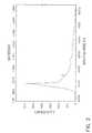
- FIG. 2is an IR spectrum of the photoluminescent output of a device formed by the process of the invention.
- a 7.6 cm diameter ultra high vacuum chemical vapor deposition (UHVCVD) reactor useful for the preparation of films of the inventionis depicted in FIG. 1.
- the reactordiffers in design from the original UHVCVD reactor described by Meyerson et al. in the article : Low temperature Si and Si: Ge epitaxy by UHVCVD, published in the IBM Journal of R&D, Vol. 34, N° 6, Nov. 1990, pp 006-015; in that pumping and wafer loading are done using the same end of the reactor.
- This modificationallows the installation of a heated precursor reservoir 1 on the opposite end of the reactor.
- the reservoiris connected to the reactor end flange using a short length of 12.7mm diameter stainless steel tubing 12.
- the reactoris constructed of quartz glass and stainless steel, using flanges, valves and seals common to the construction of high vacuum apparatus.
- the reactoris heated by external resistive heating (tube furnace 4).
- the reactoris pumped both before and during deposition by a 150 L/sec turbomolecular pump 8 backed by a two-stage oil pump 9.
- the load lock chamberis also pumped by a turbomolecular pump 10 to prevent contamination from pump oil.
- the base pressure of the reactoris below 133.3 10 -9 Pa and the load lock is capable of producing pressures below 133.3 10 -6 Pa from atmospheric pressure in less than 10 minutes.
- the precursor reservoir 1is charged with an appropriate amount of the rare earth compound and evacuated.
- the rare earthis erbium, although other rare earths, particularly terbium and europium may also be used.
- the rare earthsinclude elements 57 to 71.
- the rare earth compoundsare restricted in that they must be able to provide a vapor for the CVD process at the temperatures and pressures at which CVD can be run. In a practical sense this means that the rare earth compound should exhibit a vapor pressure of at least about 133.3 10 -6 Pa at 500°C.
- Exemplary compoundsfall into two broad categories: (a) coordination compounds, where the rare earth is bound to oxygen, nitrogen, sulfur or phosphorus, and (b) organometallic compounds, where the rare earth is bound to carbon atoms.
- Suitable ligands for the coordination compoundsinclude: acetylacetonate (2,4-pentanedionate) and derivatives of acetylacetonate including hexafluorocetylacetonate (HFAC, 1,1,1,5,5,5-hexafluoro-2,4-pentanedionate) and trifluoroacetylacetonate (TFAC, 1,1,1-trifluoro-2,4-pentanedionate); 2,4-hexanedionate and derivatives of 2,4-hexanedionate; 2,4- and 3,5-heptanedionate and derivatives including 2,2,6,6-tetramethyl 3,5-heptanedionate (THD) , 2,2,6-trimethyl 3,5-h
- organometallic compoundsinclude tris-cyclopentadienyl erbium (III) and organic derivatives of the cyclopentadienyl ring including the tris-pentamethylcyclopentadienyl ligand, the methylcyclopentadienyl ligand, and the isopropylcyclopentadienyl ligand, bis(cyclopentadienyl)erbium halides, and bis-(cyclopentadienyl)erbium alkyls, wherein alkyl is defined as a linear or branched hydrocarbon radical of one to six carbon atoms.
- Preferred ligandsinclude acetylacetonate, HFAC, THD and FOD.
- the substrateis loaded onto the quartz wafer boat 3, placed in the load-lock chamber 2 and evacuated to a suitable pressure, preferably less than 133.3 10 -5 Pa.
- the substratecan be any material that is compatible with the CVD conditions; single-crystal silicon wafers are preferred. In general, a better film is produced when the substrate wafer has been previously cleaned in the usual manner.
- a precursor gas for the semiconductor filmis introduced into the reactor.
- the precursorcan be any silane or germane or mixture of the two that is volatile under the conditions of CVD; silane (SiH 4 ), disilane (Si 2 H 6 ), germane (GeH 4 ) and digermane (Ge 2 H 6 ) are preferred.
- Group III dopant precursors, such as diborane, or group V dopant precursors, such as phosphine,may be introduced to alter the electrical properties of the films.
- the semiconductor precursor gasesare introduced via gas inlet 11 into the reactor.
- the temperature of the reactoris maintained at 450°C to 800°C. Below 450°C epitaxial growth of Si, Ge, or Si/Ge is not observed; as 900°C is approached, erbium begins to segregate.
- the pressure in the load- lock chamber 2 before introducing the substrate into the reactoris preferably below 133.3 10 -5 Pa.
- the rare earth precursoris vaporized into the reaction chamber from the reservoir 1 by applying heat.
- the heatis supplied by an external oven 7 surrounding the reservoir.
- Er(HFAC) 3the optimal rate of vaporization is obtained when the oven is held at 58° C. Regulation of the precursor reservoir temperature, and hence regulation of the partial pressure of precursor in the reactor, is important to the success of the process.
- Er(HFAC) 3at temperatures below 55°C, no erbium was incorporated. Above 65°C, the films consisted of a polycrystalline layer 30 to 40 nm thick with a concentration of erbium of 10 to 20%.
- This layerdid not increase with longer deposition times, indicating that the growth surface was "poisoned" by the precursor.
- the likely explanation for this observationis that there is a minimum growth rate above which the erbium and other elements from the precursor may be incorporated and below which the growth surface is poisoned.
- the growth rate of pure silicon from silane at 1 mtorr pressureis 4 ⁇ /min at 550°C and 40 nm/min at 650°C.
- the selection of the appropriate oven temperature for a given rare earth compoundis readily determined empirically as part of the routine adjustment of experimental conditions. Reasonable temperatures can be calculated by comparison of the vapor pressure of the precursor of interest at the pressure of the reservoir with the vapor pressure of Er(HFAC) 3 at 58°/133.3 Pa.
- the precursor reservoirwas charged with 1.0g of anhydrous tris(hexafluoroacetylacetonato-0,0') erbium (III) and evacuated.
- Anhydrous tris(hexafluoroacetylacetonato-0,0') erbium (III)was immediately placed in the reactor load-lock.
- the flow of silane (4 sccm) and hydrogen (50 sccm)was started, and the valve to the room-temperature erbium source was opened. After a ten minute pump down in the load-lock the wafers were transferred to the reactor. Three minutes after loading, the flow of hydrogen was stopped and the temperature of the reactor was increased from 500°C to 650°C over a period of one hour.
- the temperature of the oven surrounding the precursorwas increased to 58°C, directly subliming Er(HFAC) 3 into the reactor.
- the pressure during depositionwas 200 Pa, giving a calculated system pumping speed of 42 L/sec.
- the deposition rate under these conditionswas approximately 3 nm/min and deposition times varied from 3 to 12 hours.
- the flow of silanewas discontinued, and the wafers were withdrawn to the load-lock chamber to cool.
- composition of the filmswas determined using Rutherford Back Scattering spectroscopy (RBS) to determine the erbium concentration and Secondary Ion Mass Spectroscopy (SIMS) to determine the level of carbon, fluorine and oxygen present in the films.
- the carbon, oxygen, and fluorine levelswere equal in the three samples measured, within the uncertainty of the measurement. These "impurities" arise from the decomposition of the precursor.
- Sample 2was a 2 ⁇ m thick film produced by lowering T e by 2°C and growing for longer time (11 h instead of 3 h). The cross sectional TEM of this film does not show any precipitated ErSi 2 .
- the erbium concentration of sample 2was 2 x 10 19 atoms/cm 3 . This level is at least one order of magnitude higher than the highest concentrations reported using implantation techniques.
- the cross-sectional TEMalso shows a high density of threading defects. These defects may be due to stress caused by the introduction of erbium (or erbium complexes) into the film, but it is more likely that these defects are due to contamination from the precursor. At the temperatures used in UHVCVD, the crystal quality is very sensitive to the presence of carbon and oxygen and the SIMS results indicate that these elements are present in relatively high concentrations.
- One other possible source of contaminationis residual carbon and oxygen from the decomposition of the ligand upstream from the deposition zone.
- the Er(HFAC) 3 complexdecomposes in parts of the reactor which are as much as 300°C cooler and may continue to evolve small quantities of organic material which may contaminate the initial growth surface. Support for this hypothesis is given by TEM which shows that the defects occur abruptly and at highest concentration at the initial growth interface. In this respect there may be an advantage to other precursors, particularly of the organometallic type, when used together with controlled levels of oxidant gas.
- Rare earth compoundscan be prepared by methods well known in the art.
- the Er(HFAC) 3 used in the foregoing experimentwas made by a modification of the known process for the synthesis of Al(HFAC) 3 described by Morris et al. in Inorganic Syntheses, Vol. 9, S.Y. Tyree, editor; McGraw Hill, New York, (1967) p. 39. This synthesis is an improvement over the synthesis of Er(HFAC) 3 described by Berg and Acosta [Anal. Chim.
- Photoluminescence measurementswere carried out on several of the samples. Measurements were done using an Ar ion laser operating at 514 nm as the excitation source and a Cygnus FTIR to detect the emitted radiation.
- a representative spectrum of a 2 ⁇ m film with an Er concentration of 2 x 10 19 atoms/cm 3(identical to the sample used for TEM measurements above) is shown in FIG. 2. This spectrum was obtained at 10 K and the luminescence fell sharply as the temperature was raised. At 200 K, the signal intensity was down by a factor of 50 and was not observable at room temperature.
Landscapes
- Engineering & Computer Science (AREA)
- Microelectronics & Electronic Packaging (AREA)
- Condensed Matter Physics & Semiconductors (AREA)
- General Physics & Mathematics (AREA)
- Manufacturing & Machinery (AREA)
- Computer Hardware Design (AREA)
- Physics & Mathematics (AREA)
- Power Engineering (AREA)
- Chemical & Material Sciences (AREA)
- Crystallography & Structural Chemistry (AREA)
- Inorganic Chemistry (AREA)
- Materials Engineering (AREA)
- Chemical Vapour Deposition (AREA)
- Crystals, And After-Treatments Of Crystals (AREA)
Abstract
Description
Claims (18)
- A process for creating an erbium-doped semiconductorlayer on a substrate comprising introducing into afilm-forming UHVCVD chamber, for forming a deposition filmon a substrate, a mixture of a first component chosenfrom the group consisting of germanes, silanes andmixtures thereof in the gas phase and a second componentconsisting of an erbium compound in the gas phase andheating said substrate, whereby a deposition film isformed on said substrate, said erbium compound having avapor pressure greater than 133.3x10⁻⁶ Pa at 500° C.
- A process according to claim 1 additionally comprisingintroducing a source of oxygen atoms into said UHVCVDfilm-forming chamber whereby said semiconductor layercomprises said semiconductor, erbium and oxygen.
- A process according to claim 2 wherein said source ofoxygen atoms is said erbium compound.
- A process according to claim 3 wherein said erbiumcompound is chosen from the group consisting of tris(1,1,1,5,5,5-hexafluoro-2,4-pentanedionato-0,0')erbium,tris(2,4-pentanedionato-O,O')erbium, tris(1,1,1-trifluoropentanedionato-O,O')erbium,tris(1,1,1-trifluoro-5,5-dimethyl-2,4-hexanedionato-O,O')erbium,tris(5,5-dimethyl-2,4-hexanedionato-0,0')erbium,tris(1-cyclopropyl-4,4,4-trifluoro-1,3-butanedionato-0,0')erbium,tris(2,2,6-trimethyl-3,5-heptanedionato-0,0')erbium, tris(2,2,6,6-tetramethyl-3,5-heptanedionato-0,0')erbium, tris(1,1,1,5,5,6,6,7,7,7-decafluoro-2,4-heptanedionato-0,0')erbium,2,2-dimethyl-6,6,7,7,8,8,8-eptafluoro-3,5-octanedionato-0,0')erbiumand tris [(phenyliminomethyl)phenolato-O,N] erbium.
- A process according to claim 4 wherein said silane or germane is SiH4 and said erbium compound is tris1,1,1,5,5,5-hexafluoro-2,4-pentanedionato-0,0')erbium.
- A process according to claim 1 wherein said erbium-dopedsemiconductor layer contains more than 1019 atoms/cm3 oferbium.
- A process according to claim 6 wherein said erbium-dopedsemiconductor layer additionally contains at least 1018atoms/cm3 of oxygen.
- A process according to claim 1 wherein said substrate isheated at a temperature between 450° and 800°C.
- A process according to claim 2 wherein said source ofoxygen atoms is a third gaseous component.
- A process according to claim 9 wherein said thirdgaseous component is nitrous oxide.
- A process according to claim 9 wherein said erbiumcompound is chosen from the group consisting oftris (cyclopentadienyl) erbium,tris(pentamethylcyclopentadienyl)erbium,tris (methylcyclopentadienyl) erbium,tris (isopropylcyclopentadienyl) erbium,bis(cyclopentadienyl)erbium halides, andbis(cyclopentadienyl)erbium alkyls.
- A process according to claim 4 comprising the steps of:(a) introducing a silicon substrate into a film-formingUHVCVD chamber for forming a depositionfilm on a substrate;(b) introducing a flow of from 1 to 100 sccm of SiH4into said UHVCVD chamber;(c) maintaining said substrate at from 450° to 800°C;(d) maintaining the pressure in said chamber at from133.3x10 to 133.3x10⁻⁹ Pa; and(e) leading a flow of tris(1,1,1,5,5,5-hexafluoro-2,4-pentanedionato)erbiumin the gas phase into saidchamber so as to form a deposition film on saidsubstrate.
- A process according to claim 12 wherein said flow ofSiH4 is 4 sccm, said substrate is maintained at about650°C, said pressure is maintained at about 200 Pa andsaid flow of tris(1,1,1,5,5,5-hexafluoro-2,4- pentanedionato)erbiumis obtained by heating tris(1,1,1,5,5,5-hexafluoro-2,4-pentanedionato)erbium at a temperaturebetween 55 and 65°C at 200 Pa.
- A chemical vapor deposition process for creating a rareearth-doped silicon layer on a substrate wherein saidrare earth is chosen from the group consisting oferbium, terbium and europium comprising depositing saidlayer by the thermal decomposition of a gaseousprecursor mixture of a silane and a rare earth compoundin a UHVCVD chamber.
- A process according to claim 14 wherein said rareearth-doped silicon layer contains said rare earthelement in substantially a single phase at aconcentration which is higher than the equilibriumconcentration for a single phase of said rare earth insilicon.
- A process according to claim 14 wherein said gaseousprecursor mixture additionally comprises a source ofoxygen atoms.
- A process according to claim 16 wherein said source of oxygen atoms is said rare earth compound.
- A process according to claim 17 wherein said rare earthcompound is chosen from the group consisting ofhexafluoroacetylacetonates, acetylacetonates, tetramethylheptanedionatesand fluorooctanedionates.
Applications Claiming Priority (2)
| Application Number | Priority Date | Filing Date | Title |
|---|---|---|---|
| US940416 | 1992-08-31 | ||
| US07/940,416US5322813A (en) | 1992-08-31 | 1992-08-31 | Method of making supersaturated rare earth doped semiconductor layers by chemical vapor deposition |
Publications (3)
| Publication Number | Publication Date |
|---|---|
| EP0586321A2 EP0586321A2 (en) | 1994-03-09 |
| EP0586321A3 EP0586321A3 (en) | 1996-03-27 |
| EP0586321B1true EP0586321B1 (en) | 1998-05-20 |
Family
ID=25474795
Family Applications (1)
| Application Number | Title | Priority Date | Filing Date |
|---|---|---|---|
| EP93480110AExpired - LifetimeEP0586321B1 (en) | 1992-08-31 | 1993-07-30 | Formation of supersaturated rare earth doped semiconductor layers by CVD |
Country Status (11)
| Country | Link |
|---|---|
| US (3) | US5322813A (en) |
| EP (1) | EP0586321B1 (en) |
| JP (1) | JPH0785467B2 (en) |
| KR (1) | KR970008339B1 (en) |
| CN (3) | CN1054234C (en) |
| AT (1) | ATE166491T1 (en) |
| CA (1) | CA2095449C (en) |
| DE (1) | DE69318653T2 (en) |
| ES (1) | ES2116426T3 (en) |
| MX (1) | MX9305267A (en) |
| TW (1) | TW229325B (en) |
Families Citing this family (36)
| Publication number | Priority date | Publication date | Assignee | Title |
|---|---|---|---|---|
| US4873549A (en)* | 1987-03-03 | 1989-10-10 | Mita Industrial Co., Ltd. | Device for detecting the life of an image forming process unit, opening of a seal of the unit and attachment of the unit to an image forming apparatus |
| EP0650200B1 (en)* | 1993-10-20 | 1999-03-10 | Consorzio per la Ricerca sulla Microelettronica nel Mezzogiorno | Solid state electro-luminescent device and process for fabrication thereof |
| US6093246A (en)* | 1995-09-08 | 2000-07-25 | Sandia Corporation | Photonic crystal devices formed by a charged-particle beam |
| US5976941A (en)* | 1997-06-06 | 1999-11-02 | The Whitaker Corporation | Ultrahigh vacuum deposition of silicon (Si-Ge) on HMIC substrates |
| US6040225A (en)* | 1997-08-29 | 2000-03-21 | The Whitaker Corporation | Method of fabricating polysilicon based resistors in Si-Ge heterojunction devices |
| US6130471A (en)* | 1997-08-29 | 2000-10-10 | The Whitaker Corporation | Ballasting of high power silicon-germanium heterojunction biploar transistors |
| KR100377716B1 (en)* | 1998-02-25 | 2003-03-26 | 인터내셔널 비지네스 머신즈 코포레이션 | Electric pumping of rare-earth-doped silicon for optical emission |
| EP1131611A4 (en) | 1998-06-29 | 2003-01-02 | Univ State San Diego | METHOD AND APPARATUS FOR DETERMINING CARBON-HALOGENATED COMPOUNDS AND APPLICATIONS THEREOF |
| US6140669A (en)* | 1999-02-20 | 2000-10-31 | Ohio University | Gallium nitride doped with rare earth ions and method and structure for achieving visible light emission |
| US6143072A (en)* | 1999-04-06 | 2000-11-07 | Ut-Battelle, Llc | Generic process for preparing a crystalline oxide upon a group IV semiconductor substrate |
| US6255669B1 (en)* | 1999-04-23 | 2001-07-03 | The University Of Cincinnati | Visible light emitting device formed from wide band gap semiconductor doped with a rare earth element |
| KR100510996B1 (en)* | 1999-12-30 | 2005-08-31 | 주식회사 하이닉스반도체 | Method for optimizing processes of selective epitaxial growth |
| US6519543B1 (en)* | 2000-05-09 | 2003-02-11 | Agere Systems Inc. | Calibration method for quantitative elemental analysis |
| US6734453B2 (en) | 2000-08-08 | 2004-05-11 | Translucent Photonics, Inc. | Devices with optical gain in silicon |
| KR100384892B1 (en)* | 2000-12-01 | 2003-05-22 | 한국전자통신연구원 | Fabrication method of erbium-doped silicon nano-dots |
| US6894772B2 (en)* | 2001-02-12 | 2005-05-17 | Analytical Spectral Devices | System and method for grouping reflectance data |
| US6853447B2 (en)* | 2001-02-12 | 2005-02-08 | Analytical Spectral Devices, Inc. | System and method for the collection of spectral image data |
| JP2002334868A (en)* | 2001-05-10 | 2002-11-22 | Hitachi Kokusai Electric Inc | Substrate processing apparatus and semiconductor device manufacturing method |
| US20030111013A1 (en)* | 2001-12-19 | 2003-06-19 | Oosterlaken Theodorus Gerardus Maria | Method for the deposition of silicon germanium layers |
| US6771369B2 (en)* | 2002-03-12 | 2004-08-03 | Analytical Spectral Devices, Inc. | System and method for pharmacy validation and inspection |
| US20040214362A1 (en)* | 2003-01-22 | 2004-10-28 | Hill Steven E. | Doped semiconductor nanocrystal layers and preparation thereof |
| US7440180B2 (en)* | 2004-02-13 | 2008-10-21 | Tang Yin S | Integration of rare-earth doped amplifiers into semiconductor structures and uses of same |
| US7163878B2 (en)* | 2004-11-12 | 2007-01-16 | Texas Instruments Incorporated | Ultra-shallow arsenic junction formation in silicon germanium |
| CN100385693C (en)* | 2005-08-18 | 2008-04-30 | 中国科学院半导体研究所 | Method for Improving Luminescence of Silicon-based Crystal Thin Films by Plasma Treatment |
| DE102006031300A1 (en)* | 2006-06-29 | 2008-01-03 | Schmid Technology Systems Gmbh | Method for doping silicon material for solar cells, correspondingly doped silicon material and solar cell |
| US20080138955A1 (en)* | 2006-12-12 | 2008-06-12 | Zhiyuan Ye | Formation of epitaxial layer containing silicon |
| US8283201B2 (en)* | 2008-06-05 | 2012-10-09 | American Air Liquide, Inc. | Preparation of lanthanide-containing precursors and deposition of lanthanide-containing films |
| US8269253B2 (en)* | 2009-06-08 | 2012-09-18 | International Rectifier Corporation | Rare earth enhanced high electron mobility transistor and method for fabricating same |
| CN102828242B (en)* | 2012-09-06 | 2015-05-27 | 西安隆基硅材料股份有限公司 | Crystalline silicon with lower converting lighting quantum dots and preparation method thereof |
| US9481917B2 (en)* | 2012-12-20 | 2016-11-01 | United Technologies Corporation | Gaseous based desulfurization of alloys |
| WO2015017395A1 (en)* | 2013-07-30 | 2015-02-05 | Board Of Regents, The University Of Texas System | Sample transfer to high vacuum transition flow |
| US9850573B1 (en) | 2016-06-23 | 2017-12-26 | Applied Materials, Inc. | Non-line of sight deposition of erbium based plasma resistant ceramic coating |
| US10364259B2 (en)* | 2016-12-30 | 2019-07-30 | L'Air Liquide, Société Anonyme pour l'Etude et l'Exploitation des Procédés Georges Claude | Zirconium, hafnium, titanium precursors and deposition of group 4 containing films using the same |
| US10975469B2 (en) | 2017-03-17 | 2021-04-13 | Applied Materials, Inc. | Plasma resistant coating of porous body by atomic layer deposition |
| GB201812765D0 (en)* | 2018-08-06 | 2018-09-19 | Univ London Queen Mary | Substrate layer |
| CN119640395B (en)* | 2025-02-13 | 2025-07-01 | 清华大学 | Preparation method of two-dimensional monocrystal rare earth compound nano-sheet |
Family Cites Families (13)
| Publication number | Priority date | Publication date | Assignee | Title |
|---|---|---|---|---|
| DE1900116C3 (en)* | 1969-01-02 | 1978-10-19 | Siemens Ag, 1000 Berlin Und 8000 Muenchen | Process for the production of high-purity monocrystalline layers consisting of silicon |
| US4385946A (en)* | 1981-06-19 | 1983-05-31 | Bell Telephone Laboratories, Incorporated | Rapid alteration of ion implant dopant species to create regions of opposite conductivity |
| DE3319134A1 (en)* | 1983-05-26 | 1985-05-02 | Fraunhofer-Gesellschaft zur Förderung der angewandten Forschung e.V., 8000 München | Optoelectronic component, in particular a laser diode or a light-emitting diode |
| US4618381A (en)* | 1983-05-26 | 1986-10-21 | Fuji Electric Corporate Research And Development Ltd. | Method for adding impurities to semiconductor base material |
| US4800173A (en)* | 1986-02-20 | 1989-01-24 | Canon Kabushiki Kaisha | Process for preparing Si or Ge epitaxial film using fluorine oxidant |
| US4826288A (en)* | 1987-04-09 | 1989-05-02 | Polaroid Corporation, Patent Department | Method for fabricating optical fibers having cores with high rare earth content |
| US5248890A (en)* | 1989-05-13 | 1993-09-28 | Forschungszentrum Julich Gmbh | Valance specific lanthanide doped optoelectronic metal fluoride semiconductor device |
| US5296048A (en)* | 1989-05-31 | 1994-03-22 | International Business Machines Corporation | Class of magnetic materials for solid state devices |
| FR2650704B1 (en)* | 1989-08-01 | 1994-05-06 | Thomson Csf | PROCESS FOR THE MANUFACTURE BY EPITAXY OF MONOCRYSTALLINE LAYERS OF MATERIALS WITH DIFFERENT MESH PARAMETERS |
| JPH042699A (en)* | 1990-04-18 | 1992-01-07 | Mitsubishi Electric Corp | Growing of crystal |
| US5119460A (en)* | 1991-04-25 | 1992-06-02 | At&T Bell Laboratories | Erbium-doped planar optical device |
| US5107538A (en)* | 1991-06-06 | 1992-04-21 | At&T Bell Laboratories | Optical waveguide system comprising a rare-earth Si-based optical device |
| US5511946A (en)* | 1994-12-08 | 1996-04-30 | General Electric Company | Cooled airfoil tip corner |
- 1992
- 1992-08-31USUS07/940,416patent/US5322813A/ennot_activeExpired - Lifetime
- 1993
- 1993-05-04CACA002095449Apatent/CA2095449C/ennot_activeExpired - Fee Related
- 1993-07-28JPJP5185980Apatent/JPH0785467B2/ennot_activeExpired - Fee Related
- 1993-07-30ESES93480110Tpatent/ES2116426T3/ennot_activeExpired - Lifetime
- 1993-07-30EPEP93480110Apatent/EP0586321B1/ennot_activeExpired - Lifetime
- 1993-07-30DEDE69318653Tpatent/DE69318653T2/ennot_activeExpired - Lifetime
- 1993-07-30ATAT93480110Tpatent/ATE166491T1/enactive
- 1993-08-19TWTW082106685Apatent/TW229325B/zhnot_activeIP Right Cessation
- 1993-08-30MXMX9305267Apatent/MX9305267A/ennot_activeIP Right Cessation
- 1993-08-30CNCN93117079Apatent/CN1054234C/ennot_activeExpired - Fee Related
- 1993-08-30KRKR1019930017032Apatent/KR970008339B1/ennot_activeExpired - Fee Related
- 1994
- 1994-03-09USUS08/207,942patent/US5534079A/ennot_activeExpired - Lifetime
- 1995
- 1995-06-06USUS08/468,367patent/US5646425A/ennot_activeExpired - Fee Related
- 1999
- 1999-11-09CNCN99123482Apatent/CN1114225C/ennot_activeExpired - Fee Related
- 1999-11-09CNCN99123481Apatent/CN1117389C/ennot_activeExpired - Fee Related
Also Published As
| Publication number | Publication date |
|---|---|
| US5646425A (en) | 1997-07-08 |
| ATE166491T1 (en) | 1998-06-15 |
| CA2095449C (en) | 1997-09-16 |
| CN1085353A (en) | 1994-04-13 |
| KR970008339B1 (en) | 1997-05-23 |
| CA2095449A1 (en) | 1994-03-01 |
| CN1255736A (en) | 2000-06-07 |
| CN1114225C (en) | 2003-07-09 |
| EP0586321A3 (en) | 1996-03-27 |
| EP0586321A2 (en) | 1994-03-09 |
| DE69318653T2 (en) | 1999-02-04 |
| US5322813A (en) | 1994-06-21 |
| DE69318653D1 (en) | 1998-06-25 |
| MX9305267A (en) | 1994-02-28 |
| US5534079A (en) | 1996-07-09 |
| CN1054234C (en) | 2000-07-05 |
| CN1255735A (en) | 2000-06-07 |
| TW229325B (en) | 1994-09-01 |
| JPH0785467B2 (en) | 1995-09-13 |
| KR940004714A (en) | 1994-03-15 |
| ES2116426T3 (en) | 1998-07-16 |
| JPH06177062A (en) | 1994-06-24 |
| CN1117389C (en) | 2003-08-06 |
Similar Documents
| Publication | Publication Date | Title |
|---|---|---|
| EP0586321B1 (en) | Formation of supersaturated rare earth doped semiconductor layers by CVD | |
| US5296258A (en) | Method of forming silicon carbide | |
| Kuech et al. | Disilane: A new silicon doping source in metalorganic chemical vapor deposition of GaAs | |
| US5300185A (en) | Method of manufacturing III-V group compound semiconductor | |
| US4830982A (en) | Method of forming III-V semi-insulating films using organo-metallic titanium dopant precursors | |
| Reep et al. | Electrical properties of organometallic chemical vapor deposited GaAs epitaxial layers: temperature dependence | |
| US3836408A (en) | Production of epitaxial films of semiconductor compound material | |
| US5410178A (en) | Semiconductor films | |
| Rogers et al. | Erbium‐doped silicon films grown by plasma‐enhanced chemical‐vapor deposition | |
| US4782034A (en) | Semi-insulating group III-V based compositions doped using bis arene titanium sources | |
| KR100923937B1 (en) | Method of manufacturing a semiconductor material and device whose electrical conductivity is controlled | |
| JPH0253097B2 (en) | ||
| Beach et al. | Erbium-Doped Silicon Prepared by UHV/CVD | |
| Greenwald et al. | Mocvd Erbium Sourcesa | |
| EP0293439B1 (en) | Semi-insulating group iii-v based compositions | |
| US7329554B2 (en) | Reactive codoping of GaAlInP compound semiconductors | |
| US5306660A (en) | Technique for doping mercury cadmium telluride MOCVD grown crystalline materials using free radical transport of elemental indium and apparatus therefor | |
| Smith | Epitaxial growth of GaAs by low-pressure MOCVD | |
| JPS60169563A (en) | Manufacture and device for telluride metal | |
| EP0141561B1 (en) | A process for producing devices having semi-insulating indium phosphide based compositions | |
| Andry et al. | Low-Temperature Growth of Si: Er by Electron Cyclotron Resonance Pecvd Using Metal Organics | |
| Babushkina et al. | Effects of growth conditions on the photoluminescence spectra of epitaxial GaAs films made by the hydride method | |
| Vrahue | Low Temperature Epitaxial Growth of Rare Earth Doped Silicon and Silicon Germanium Alloys. | |
| Park | Final Technical Report for: ErAs/GaAs SUPERLATTICE INFRARED DETECTOR BY CHEMICAL VAPOR DEPOSITION | |
| JPH0786186A (en) | Method for producing p-type thin film of II-VI compound semiconductor |
Legal Events
| Date | Code | Title | Description |
|---|---|---|---|
| PUAI | Public reference made under article 153(3) epc to a published international application that has entered the european phase | Free format text:ORIGINAL CODE: 0009012 | |
| AK | Designated contracting states | Kind code of ref document:A2 Designated state(s):AT BE CH DE ES FR GB IT LI NL SE | |
| 17P | Request for examination filed | Effective date:19940627 | |
| PUAL | Search report despatched | Free format text:ORIGINAL CODE: 0009013 | |
| AK | Designated contracting states | Kind code of ref document:A3 Designated state(s):AT BE CH DE ES FR GB IT LI NL SE | |
| 17Q | First examination report despatched | Effective date:19960603 | |
| GRAG | Despatch of communication of intention to grant | Free format text:ORIGINAL CODE: EPIDOS AGRA | |
| RTI1 | Title (correction) | ||
| GRAG | Despatch of communication of intention to grant | Free format text:ORIGINAL CODE: EPIDOS AGRA | |
| GRAH | Despatch of communication of intention to grant a patent | Free format text:ORIGINAL CODE: EPIDOS IGRA | |
| GRAH | Despatch of communication of intention to grant a patent | Free format text:ORIGINAL CODE: EPIDOS IGRA | |
| GRAA | (expected) grant | Free format text:ORIGINAL CODE: 0009210 | |
| AK | Designated contracting states | Kind code of ref document:B1 Designated state(s):AT BE CH DE ES FR GB IT LI NL SE | |
| REF | Corresponds to: | Ref document number:166491 Country of ref document:AT Date of ref document:19980615 Kind code of ref document:T | |
| REG | Reference to a national code | Ref country code:CH Ref legal event code:NV Representative=s name:CARL O. BARTH C/O IBM CORPORATION ZURICH INTELLECT Ref country code:CH Ref legal event code:EP | |
| REF | Corresponds to: | Ref document number:69318653 Country of ref document:DE Date of ref document:19980625 | |
| REG | Reference to a national code | Ref country code:ES Ref legal event code:FG2A Ref document number:2116426 Country of ref document:ES Kind code of ref document:T3 | |
| ITF | It: translation for a ep patent filed | ||
| ET | Fr: translation filed | ||
| PGFP | Annual fee paid to national office [announced via postgrant information from national office to epo] | Ref country code:CH Payment date:19981027 Year of fee payment:6 | |
| PLBE | No opposition filed within time limit | Free format text:ORIGINAL CODE: 0009261 | |
| STAA | Information on the status of an ep patent application or granted ep patent | Free format text:STATUS: NO OPPOSITION FILED WITHIN TIME LIMIT | |
| 26N | No opposition filed | ||
| PGFP | Annual fee paid to national office [announced via postgrant information from national office to epo] | Ref country code:AT Payment date:19990729 Year of fee payment:7 | |
| PG25 | Lapsed in a contracting state [announced via postgrant information from national office to epo] | Ref country code:LI Free format text:LAPSE BECAUSE OF NON-PAYMENT OF DUE FEES Effective date:19990731 Ref country code:CH Free format text:LAPSE BECAUSE OF NON-PAYMENT OF DUE FEES Effective date:19990731 | |
| REG | Reference to a national code | Ref country code:CH Ref legal event code:PL | |
| PG25 | Lapsed in a contracting state [announced via postgrant information from national office to epo] | Ref country code:AT Free format text:LAPSE BECAUSE OF NON-PAYMENT OF DUE FEES Effective date:20000730 | |
| PGFP | Annual fee paid to national office [announced via postgrant information from national office to epo] | Ref country code:BE Payment date:20000807 Year of fee payment:8 | |
| PG25 | Lapsed in a contracting state [announced via postgrant information from national office to epo] | Ref country code:BE Free format text:LAPSE BECAUSE OF NON-PAYMENT OF DUE FEES Effective date:20010731 | |
| REG | Reference to a national code | Ref country code:GB Ref legal event code:IF02 | |
| BERE | Be: lapsed | Owner name:INTERNATIONAL BUSINESS MACHINES CORP. Effective date:20010731 | |
| PGFP | Annual fee paid to national office [announced via postgrant information from national office to epo] | Ref country code:FR Payment date:20020715 Year of fee payment:10 | |
| PG25 | Lapsed in a contracting state [announced via postgrant information from national office to epo] | Ref country code:FR Free format text:LAPSE BECAUSE OF NON-PAYMENT OF DUE FEES Effective date:20040331 | |
| REG | Reference to a national code | Ref country code:FR Ref legal event code:ST | |
| PGFP | Annual fee paid to national office [announced via postgrant information from national office to epo] | Ref country code:IT Payment date:20060731 Year of fee payment:14 | |
| REG | Reference to a national code | Ref country code:GB Ref legal event code:746 Effective date:20080704 | |
| PGFP | Annual fee paid to national office [announced via postgrant information from national office to epo] | Ref country code:ES Payment date:20080707 Year of fee payment:16 | |
| PGFP | Annual fee paid to national office [announced via postgrant information from national office to epo] | Ref country code:NL Payment date:20080731 Year of fee payment:16 | |
| PG25 | Lapsed in a contracting state [announced via postgrant information from national office to epo] | Ref country code:IT Free format text:LAPSE BECAUSE OF NON-PAYMENT OF DUE FEES Effective date:20070730 | |
| PGFP | Annual fee paid to national office [announced via postgrant information from national office to epo] | Ref country code:SE Payment date:20090730 Year of fee payment:17 | |
| NLV4 | Nl: lapsed or anulled due to non-payment of the annual fee | Effective date:20100201 | |
| REG | Reference to a national code | Ref country code:ES Ref legal event code:FD2A Effective date:20090731 | |
| PG25 | Lapsed in a contracting state [announced via postgrant information from national office to epo] | Ref country code:ES Free format text:LAPSE BECAUSE OF NON-PAYMENT OF DUE FEES Effective date:20090731 | |
| PG25 | Lapsed in a contracting state [announced via postgrant information from national office to epo] | Ref country code:NL Free format text:LAPSE BECAUSE OF NON-PAYMENT OF DUE FEES Effective date:20100201 Ref country code:SE Free format text:LAPSE BECAUSE OF NON-PAYMENT OF DUE FEES Effective date:20100731 | |
| PGFP | Annual fee paid to national office [announced via postgrant information from national office to epo] | Ref country code:GB Payment date:20120723 Year of fee payment:20 | |
| PGFP | Annual fee paid to national office [announced via postgrant information from national office to epo] | Ref country code:DE Payment date:20120723 Year of fee payment:20 | |
| REG | Reference to a national code | Ref country code:DE Ref legal event code:R071 Ref document number:69318653 Country of ref document:DE | |
| REG | Reference to a national code | Ref country code:DE Ref legal event code:R071 Ref document number:69318653 Country of ref document:DE | |
| REG | Reference to a national code | Ref country code:GB Ref legal event code:PE20 Expiry date:20130729 | |
| PG25 | Lapsed in a contracting state [announced via postgrant information from national office to epo] | Ref country code:DE Free format text:LAPSE BECAUSE OF EXPIRATION OF PROTECTION Effective date:20130731 | |
| PG25 | Lapsed in a contracting state [announced via postgrant information from national office to epo] | Ref country code:GB Free format text:LAPSE BECAUSE OF EXPIRATION OF PROTECTION Effective date:20130729 | |
| REG | Reference to a national code | Ref country code:DE Ref legal event code:R081 Ref document number:69318653 Country of ref document:DE Owner name:GLOBALFOUNDRIES INC., KY Free format text:FORMER OWNER: INTERNATIONAL BUSINESS MACHINES CORPORATION, ARMONK, NY, US Ref country code:DE Ref legal event code:R082 Ref document number:69318653 Country of ref document:DE Representative=s name:RICHARDT PATENTANWAELTE PARTG MBB, DE Ref country code:DE Ref legal event code:R081 Ref document number:69318653 Country of ref document:DE Owner name:GLOBALFOUNDRIES INC., KY Free format text:FORMER OWNER: INTERNATIONAL BUSINESS MACHINES CORPORATION, ARMONK, N.Y., US | |
| REG | Reference to a national code | Ref country code:DE Ref legal event code:R082 Ref document number:69318653 Country of ref document:DE Representative=s name:RICHARDT PATENTANWAELTE PARTG MBB, DE Ref country code:DE Ref legal event code:R081 Ref document number:69318653 Country of ref document:DE Owner name:GLOBALFOUNDRIES INC., KY Free format text:FORMER OWNER: GLOBALFOUNDRIES US 2 LLC (N.D.GES.DES STAATES DELAWARE), HOPEWELL JUNCTION, N.Y., US | |
| REG | Reference to a national code | Ref country code:FR Ref legal event code:TP Owner name:GLOBALFOUNDRIES INC., GB Effective date:20160829 |