EP0571092B1 - Single in-line memory module - Google Patents
Single in-line memory moduleDownload PDFInfo
- Publication number
- EP0571092B1 EP0571092B1EP93303345AEP93303345AEP0571092B1EP 0571092 B1EP0571092 B1EP 0571092B1EP 93303345 AEP93303345 AEP 93303345AEP 93303345 AEP93303345 AEP 93303345AEP 0571092 B1EP0571092 B1EP 0571092B1
- Authority
- EP
- European Patent Office
- Prior art keywords
- memory module
- circuit board
- printed circuit
- computer system
- contact pads
- Prior art date
- Legal status (The legal status is an assumption and is not a legal conclusion. Google has not performed a legal analysis and makes no representation as to the accuracy of the status listed.)
- Expired - Lifetime
Links
Images


Classifications
- G—PHYSICS
- G11—INFORMATION STORAGE
- G11C—STATIC STORES
- G11C5/00—Details of stores covered by group G11C11/00
- G11C5/02—Disposition of storage elements, e.g. in the form of a matrix array
- G11C5/04—Supports for storage elements, e.g. memory modules; Mounting or fixing of storage elements on such supports
- G—PHYSICS
- G11—INFORMATION STORAGE
- G11C—STATIC STORES
- G11C5/00—Details of stores covered by group G11C11/00
- H—ELECTRICITY
- H05—ELECTRIC TECHNIQUES NOT OTHERWISE PROVIDED FOR
- H05K—PRINTED CIRCUITS; CASINGS OR CONSTRUCTIONAL DETAILS OF ELECTRIC APPARATUS; MANUFACTURE OF ASSEMBLAGES OF ELECTRICAL COMPONENTS
- H05K1/00—Printed circuits
- H05K1/02—Details
- H05K1/11—Printed elements for providing electric connections to or between printed circuits
- H05K1/117—Pads along the edge of rigid circuit boards, e.g. for pluggable connectors
- H—ELECTRICITY
- H05—ELECTRIC TECHNIQUES NOT OTHERWISE PROVIDED FOR
- H05K—PRINTED CIRCUITS; CASINGS OR CONSTRUCTIONAL DETAILS OF ELECTRIC APPARATUS; MANUFACTURE OF ASSEMBLAGES OF ELECTRICAL COMPONENTS
- H05K1/00—Printed circuits
- H05K1/02—Details
- H05K1/14—Structural association of two or more printed circuits
- H05K1/141—One or more single auxiliary printed circuits mounted on a main printed circuit, e.g. modules, adapters
- H—ELECTRICITY
- H05—ELECTRIC TECHNIQUES NOT OTHERWISE PROVIDED FOR
- H05K—PRINTED CIRCUITS; CASINGS OR CONSTRUCTIONAL DETAILS OF ELECTRIC APPARATUS; MANUFACTURE OF ASSEMBLAGES OF ELECTRICAL COMPONENTS
- H05K1/00—Printed circuits
- H05K1/18—Printed circuits structurally associated with non-printed electric components
- H05K1/181—Printed circuits structurally associated with non-printed electric components associated with surface mounted components
- H—ELECTRICITY
- H05—ELECTRIC TECHNIQUES NOT OTHERWISE PROVIDED FOR
- H05K—PRINTED CIRCUITS; CASINGS OR CONSTRUCTIONAL DETAILS OF ELECTRIC APPARATUS; MANUFACTURE OF ASSEMBLAGES OF ELECTRICAL COMPONENTS
- H05K2201/00—Indexing scheme relating to printed circuits covered by H05K1/00
- H05K2201/09—Shape and layout
- H05K2201/09209—Shape and layout details of conductors
- H05K2201/095—Conductive through-holes or vias
- H05K2201/09645—Patterning on via walls; Plural lands around one hole
- H—ELECTRICITY
- H05—ELECTRIC TECHNIQUES NOT OTHERWISE PROVIDED FOR
- H05K—PRINTED CIRCUITS; CASINGS OR CONSTRUCTIONAL DETAILS OF ELECTRIC APPARATUS; MANUFACTURE OF ASSEMBLAGES OF ELECTRICAL COMPONENTS
- H05K2201/00—Indexing scheme relating to printed circuits covered by H05K1/00
- H05K2201/10—Details of components or other objects attached to or integrated in a printed circuit board
- H05K2201/10613—Details of electrical connections of non-printed components, e.g. special leads
- H05K2201/10621—Components characterised by their electrical contacts
- H05K2201/10689—Leaded Integrated Circuit [IC] package, e.g. dual-in-line [DIL]
- H—ELECTRICITY
- H05—ELECTRIC TECHNIQUES NOT OTHERWISE PROVIDED FOR
- H05K—PRINTED CIRCUITS; CASINGS OR CONSTRUCTIONAL DETAILS OF ELECTRIC APPARATUS; MANUFACTURE OF ASSEMBLAGES OF ELECTRICAL COMPONENTS
- H05K2203/00—Indexing scheme relating to apparatus or processes for manufacturing printed circuits covered by H05K3/00
- H05K2203/15—Position of the PCB during processing
- H05K2203/1572—Processing both sides of a PCB by the same process; Providing a similar arrangement of components on both sides; Making interlayer connections from two sides
- H—ELECTRICITY
- H05—ELECTRIC TECHNIQUES NOT OTHERWISE PROVIDED FOR
- H05K—PRINTED CIRCUITS; CASINGS OR CONSTRUCTIONAL DETAILS OF ELECTRIC APPARATUS; MANUFACTURE OF ASSEMBLAGES OF ELECTRICAL COMPONENTS
- H05K3/00—Apparatus or processes for manufacturing printed circuits
- H05K3/40—Forming printed elements for providing electric connections to or between printed circuits
- H05K3/403—Edge contacts; Windows or holes in the substrate having plural connections on the walls thereof
- Y—GENERAL TAGGING OF NEW TECHNOLOGICAL DEVELOPMENTS; GENERAL TAGGING OF CROSS-SECTIONAL TECHNOLOGIES SPANNING OVER SEVERAL SECTIONS OF THE IPC; TECHNICAL SUBJECTS COVERED BY FORMER USPC CROSS-REFERENCE ART COLLECTIONS [XRACs] AND DIGESTS
- Y10—TECHNICAL SUBJECTS COVERED BY FORMER USPC
- Y10S—TECHNICAL SUBJECTS COVERED BY FORMER USPC CROSS-REFERENCE ART COLLECTIONS [XRACs] AND DIGESTS
- Y10S439/00—Electrical connectors
- Y10S439/951—PCB having detailed leading edge
Definitions
- the present inventionrelates to the field of computer systems and memory hardware. More particularly, the present invention relates to modular circuit boards which may be combined to form a memory structure within a computer system.
- SIMMsSingle In-Line Memory Modules
- SIMMswere developed to provide compact and easy to manage modular memory components for user installation in computer systems designed to accept such SIMMs.
- SIMMsgenerally are easily inserted into a connector within the computer system, the SIMM thereby deriving all necessary power, ground, and logic signals therefrom.
- a SIMMtypically comprises a multiplicity of random access memory (“RAM”) chips mounted to a printed circuit board.
- the RAM memory chipsmay be dynamic RAM (DRAM), non volatile static RAM (SRAM) or video RAM (VRAM).
- DRAM memoriesare larger and cheaper than memory cells for SRAMs, DRAMs are widely used as the principal building block for main memories in computer systems.
- SRAM and VRAM SIMMshave more limited application for special purposes such as extremely fast cache memories and video frame buffers, respectively. Because DRAMs form the largest portion of a computer system memory, it is therefore desirable that memory modules flexibly accommodate the computation needs of a user as the users' requirements change over time.
- SIMM modulesmay be added to the computer system with a minimum user difficulty, specifically in terms of configuration of a SIMM within a particular memory structure.
- SIMMshave generally been designed to provide memory increments of one or more megabytes (MB), but where the memory addition comprises only a portion of the full data path used in the computer system.
- MBmegabytes
- a leading example of the prior art organization and structureis that disclosed in U.S. Patent No. 4,656,605, issued April 7, 1987 to Clayton. Clayton discloses a compact modular memory circuit board to which are mounted nine memory chips which are arranged to provide memory increments in eight bit (one byte) data widths, plus parity bits.
- the SIMM constructed according to Claytoncannot provide a memory increment for the entire data path. Instead the user must obtain and install multiple SIMMs, in combination with performing any additional configuration requirements necessary to make the separate SIMMs modules function as a single memory unit, such as setting base addresses for the SIMM modules installed.
- SIMMs constructed according to the prior arttypically must insert multiple SIMMs to achieve a memory expansion for the entire data path of his computer.
- the foregoingis a consequence of typical prior art SIMM architecture, wherein the SIMM is arranged around DRAM parts which comprise one byte wide memory increments.
- DRAM partswhich comprise one byte wide memory increments.
- EP-A-0 089 248discloses a semiconductor device comprising a plurality of leadless packages mounted on both sides of a base plate. A plurality of lead pins projects from one edge of the base plate.
- EP-A-0 419 863discloses memory modules that can be configured to provide 32 bit, 64 bit or wider data I/O, and can also be configured to provide smaller word sizes.
- the present inventionprovides, among other attributes, facility for providing memory expansion in full data path widths, thereby relieving the user of configuring and installing multiple SIMMs modules to obtain any desired memory increment.
- SIMMdynamic random access memory
- a printed circuit board having a multiplicity of DRAM memory elements mounted theretois arranged in a data path having a width of 144 bits.
- the SIMM of the present inventionfurther includes on-board drivers to buffer and drive signals in close proximity to the memory elements.
- electrically conductive tracesare routed on the circuit board in such a manner to reduce loading and trace capacitance to minimize signal skew to the distributed memory elements.
- the SIMMfurther includes a high pin density dual read-out connector structure receiving electrical traces from both sides of the circuit board for enhanced functionality.
- the SIMMis installed in complementary sockets one SIMM at a time to provide memory expansion in full width increments.
- symmetrical power and ground routings to the connector structureinsure that the SIMM cannot be inserted incorrectly, wherein physically reversing the SIMM in the connector slot will not reverse power the SIMM.
- Figure 1aillustrates the electrical schematic of a first side of the single in-line memory module (SIMM) according to the teachings of the present invention.
- Figure 1billustrates the electrical schematic for a left-to-right mirror image layout of memory elements on a second side of the SIMM.
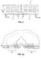
- Figure 2illustrates the physical layout of the memory elements and drivers placed on the SIMM.
- Figure 2ais a magnified view of the dual read-out connector structure on the SIMM.
- Figure 3illustrates the stacked conductive layers separated by insulating dielectric necessary to build up the interconnections for the electrical schematic shown in Figures 1a and 1b.
- Figure 4is a description of data, address and logic lines summary of address, data and control signals routed to the SIMM.
- Figure 5illustrates the pin arrangement on the high pin density dual read-out connector structure used to interconnect the SIMM with the memory system.
- Figure 6is a pinout summary for signals transmitted to and from the SIMM.
- a bus architecture for integrated data and video memoryis disclosed.
- specific numbers, times, signals etc.are set forth in order to provide a thorough understanding of the present invention.
- the present inventionmay be practiced without these specific details.
- well known circuits and devicesare shown in block diagram form in order not to obscure the present invention unnecessarily.
- SIMMintegrated data and video memory bus
- U.S. Patent 5,266,218entitled "A Bus Architecture for Integrated Data and Video Memory”.
- FIG. 1aan electrical block diagram of memory elements mounted to a first, obverse side of the SIMM is shown.
- a multiplicity of dynamic RAM (DRAMs) 10are grouped into two clusters 10a and 10b . There are nine DRAMs 10 in each cluster.
- a driver 15receives control signals, and address signals from an external bus arrangement (not shown) through a dual sided connector 30 .
- a multiplicity of control lines 20route RAS-(row access strobe), CAS- (column access strobe), WE- (write enable), and OE- (output enable), control signals from driver 15 to all the DRAMs 10 mounted to SIMM 5 .
- driver 15buffers and subsequently distributes address signals 21 to all DRAM's 10 mounted to SIMM 5 .
- all DRAMs 10have four data lines DRAMs 10 being any of several commercially available DRAMs arranged in a "by-four" configuration.
- DRAMs 10 each of DRAM clusters 10a and 10bare matched with mirror image DRAMs 10 mounted to the opposite side of SIMM 5 and placed in electrical communication by electrical traces passing through a multiplicity of vias (not shown).
- SIMM 5The specific routing of the electrical traces on SIMM 5 are dependent upon the specific architecture of the memory chips chosen for a specific implementation of SIMM 5 . However, all SIMMs 5 constructed according to the teachings of the present invention have a full width data path extending from connector 30 to all devices operating on SIMM 5 , including all DRAMs 10 , driver 15 , and any other logic elements necessary to implement the desired function of SIMM 5 . As presently preferred, SIMM 5 embodies a 144 bit data path, comprising 128 data lines (DATA[127:0]), 16 error correction lines (CBW[15:0]) which implement a known error correction code, one RAS-, two CAS- signals, one WE signal and one reset line.
- DATA[127:0]128 data lines
- CBW[15:0]16 error correction lines
- the routing for all control signals 20 , address signals 21 and data signals 25minimize conductive trace capacitance and loading in accordance with above referenced U.S. Pat. 5,260,892 entitled "High Speed Electric Signal Interconnect Structure,"
- the trace routing control for all control signals 20are taken from driver 15 to the central DRAM 10 for each DRAM cluster 10a, 10b , 10c , and 10d .
- DRAMs surrounding the central DRAM 10are coupled to control signals 20 via short sub traces (not shown), thereby minimizing total capacitance, and increasing signal rise times.
- SIMM 5With brief reference to Figure 1b , a second, reverse side of SIMM 5 is shown.
- two additional DRAM clusters 10c and 10dare shown arranged as DRAM clusters 10a and 10b on the obverse side.
- Each DRAM 10 in DRAM clusters 10c and 10dsimilarly receives four input lines in addition to address and control lines passed from driver 15 on the obverse side through conductive vias to the mirror image reverse side of SIMM 5 ., thereby doubling the available surface area to which DRAMs 10 may be mounted.
- SIMM 5as presently preferred utilized thin small outline package (TSOP) DRAMs 10 to reduce overall thickness of SIMMs 5 .
- TSOPthin small outline package
- SIMM 5the high number density connector 30 used to connect SIMM 5 to the memory module socket (not shown) is illustrated.
- connector 30is seen to have 200 pin terminations, therefore permitting a large number of signals to be routed to and from SIMM 5 .
- SIMM 5specifically incorporate the data path architecture consistent with an integrated data and video memory bus such as that described in above referenced U.S. Patent 5,266,218.
- the data path architecture implemented on SIMM 5includes 128 data lines, 16 error correction code lines (referred to CBW [15:0] in Figures 1-6 ), in addition to a multiplicity of control signals necessary to accomplish DRAM memory accesses.
- control signalscollectively referred to control lines 20 in Figures 1a and 1b , include one RAS- per SIMM 5 , two CAS- signals, one WE-, and one reset line.
- the data path used for transmission of data to and from DRAMs 10is seen to be 144 bites wide.
- the error correction code signals referred to in Figures 1-6 as CBW[15:0]the actual data path width of SIMM 5 for writing and reading data to and from memory is 128 bits wide, or sixteen bytes, identical to that of the integrated data and video memory bus. Accordingly, SIMM 5 of the present invention may be installed into the memory bus in full width increments.
- a total memory capacity available on a SIMM 5may be computed as follows. Depending on the capacity of each RAM 10 mounted to SIMM 5 the total memory capacity of each SIMM module 5 can vary from four megabytes (MB) to a maximum of sixty-four MB, distributed over a total of thirty-six DRAMs 10 . Using commercially available 256K x 4 1 Mbit DRAMs 10 , four megabytes of memory may be provided on SIMM 5 . Alternatively, when 16 megabit parts become available, because the addressable address space of SIMM 5 is very large, greater than two gigabits, SIMM 5 can easily accommodate the higher 16 megabyte parts and make available a total capacity of 64 megabit on a SIMM 5 having 36 DRAMs mounted to it.
- SIMM 5Operation of SIMM 5 is controlled by control signals 20 as will be briefly discussed below.
- control signals 20For a complete discussion on the actual operation of SIMM 5 in connection with the integrated data and video bus, the reader is referred to the above U.S. Patent 5,266,218 entitled "A Bus Architecture".
- FIG. 2wherein the physical arrangement of DRAMs 10 and driver 15 are illustrated on SIMM 5 .
- the SIMM 5is noted to have two contact regions 50a and 50b on the lower edge of SIMM 5 .
- Contact regions 50a and 50bconsist of narrowly spaced conductive contact pads running longitudinally across the bottom edge of SIMM 5 from pin 0 to pin 199, corresponding in number to the connector map (shown in Figure 4 ) and the pinout summary (shown in Figure 6 ).
- FIG 2a detail of the bottom edge of SIMM 5 is shown in Figure 2a , a magnified view of the contact region of contact regions 50a and 50b are shown in perspective view.
- contact regions 50a and 50bconsist of a large number of closely spaced contact pads 35 on the obverse side of SIMM 5 and a mirror image yet electrically distinct set of contact pads 36 on the reverse side of SIMM 5 .
- the SIMM 5 of the present inventiondoubles the pinout capacity of a SIMM by "breaking" the connection between the obverse and reverse sides of SIMM 5 , thereby effectively doubling the edge area which may be dedicated to electrical functions.
- the spacing of contacts 35 and 36 on SIMM 5are placed on 0.050" centers, the contact pads 35 and 36 themselves being 0.040" in lateral dimension thereby yielding a space of 0.010" between contact pads.
- the precise spacing and dimensionsis not specific to the present invention, and it will be obvious to those skilled in the art that numerous spacing and pad placement schemes are possible using the "dual read out" arrangement as illustrated in Figure 2a in contact regions 50a and 50b .
- the reduced spacing and dual readout arrangement of contact regions 50a and 50bprovide a vastly improved pinout density available for SIMM modules, over four times that suggested by Clayton.
- the full data path width of 144 bits in addition to control signals and power and ground connectionsis accommodated by connector 30 and connector regions 50a and 50b of SIMM 5 .
- SIMM 5constructed according to the teachings of the present invention is that memory expansion may be accommodated in full data path width increments.
- memorymay be expanded one SIMM at a time, and does not require multiple modules to be inserted to gain a single increment in memory expansion. The above result is principally derived from the accommodation of a full data path signal path on SIMM 5 , thus facilitating easy installation of additional memory.
- connector 30further provides for power and ground to be connected to all DRAMs 10 and driver 15 .
- all power and ground leadsare symmetrically arranged within Connector 30 , as is more clearly seen in Figure 6 .
- Power (VCC) and ground (GND) leadsare seen to alternate every sixteen pins. If a SIMMS were inadvertently inserted in a reversed position into a memory module socket, the symmetrical power ground leads prevent the SIMM 5 from being reverse-powered, and likely destroyed.
- SIMM 5may be used with memory arrangements other than the integrated data and video memory incorporated by reference from the above-referenced US Patent 5,266,218.
- SIMM 5is optimally designed for use in the integrated video memory, and the user would derive optimal benefit from use in such a system.
Landscapes
- Engineering & Computer Science (AREA)
- Microelectronics & Electronic Packaging (AREA)
- Dram (AREA)
- Coupling Device And Connection With Printed Circuit (AREA)
- Credit Cards Or The Like (AREA)
- Techniques For Improving Reliability Of Storages (AREA)
- Memory System (AREA)
Description
- This application is related to U.S. Patent5,260,892 entitled "High-Speed Electrical Signal InterconnectStructure", issued November 9, 1993, and U.S. Patent 5,266,218entitled "Bus Architecture for Integrated Data andVideo Memory", issued November 23, 1993.
- The present invention relates to the field of computer systemsand memory hardware. More particularly, the present inventionrelates to modular circuit boards which may be combined to form a memorystructure within a computer system.
- Single In-Line Memory Modules ("SIMMs") are compact circuitboards designed to accommodate surface mount memory chips.SIMMs were developed to provide compact and easy to managemodular memory components for user installation in computersystems designed to accept such SIMMs. SIMMs generally are easilyinserted into a connector within the computer system, the SIMMthereby deriving all necessary power, ground, and logic signalstherefrom.
- A SIMM typically comprises a multiplicity of random accessmemory ("RAM") chips mounted to a printed circuit board.Depending on the user's needs, the RAM memory chips may bedynamic RAM (DRAM), non volatile static RAM (SRAM) or videoRAM (VRAM). Because DRAM memories are larger and cheaper thanmemory cells for SRAMs, DRAMs are widely used as the principalbuilding block for main memories in computer systems. SRAM andVRAM SIMMs have more limited application for special purposessuch as extremely fast cache memories and video frame buffers,respectively. Because DRAMs form the largest portion of a computersystem memory, it is therefore desirable that memory modules flexiblyaccommodate the computation needs of a user as the users'requirements change over time. Moreover, it is desirable that the SIMMmodules may be added to the computer system with a minimum userdifficulty, specifically in terms of configuration of a SIMM within aparticular memory structure. In the past, SIMMs have generally beendesigned to provide memory increments of one or more megabytes(MB), but where the memory addition comprises only a portion of thefull data path used in the computer system. A leading example of theprior art organization and structure is that disclosed in U.S. Patent No.4,656,605, issued April 7, 1987 to Clayton. Clayton discloses a compactmodular memory circuit board to which are mounted nine memorychips which are arranged to provide memory increments in eight bit(one byte) data widths, plus parity bits. Thus, because most computersystems use data paths of 32, 64 or more bits, the SIMM constructedaccording to Clayton cannot provide a memory increment for the entire data path. Instead the user must obtain and install multipleSIMMs, in combination with performing any additional configurationrequirements necessary to make the separate SIMMs modules functionas a single memory unit, such as setting base addresses for the SIMMmodules installed.
- As a result, a user seeking to increase his usable main memoryby adding SIMMs constructed according to the prior art, typically mustinsert multiple SIMMs to achieve a memory expansion for the entiredata path of his computer. The foregoing is a consequence of typicalprior art SIMM architecture, wherein the SIMM is arranged aroundDRAM parts which comprise one byte wide memory increments. Thusin a data path having a width of 32 bits, there being eight bits per byte,a 1 megabyte expansion of main memory using SIMMs constructedaccording to the prior art would require four SIMM modules each ofone megabyte capacity in order to obtain a full data path expansion ofone megabyte.
- EP-A-0 089 248 discloses a semiconductor device comprising aplurality of leadless packages mounted on both sides of a baseplate. A plurality of lead pins projects from one edge of thebase plate.
- The article "High performance package for memory" by V.Y. Dooet al. in IBM Technical Disclosure Bulletin, vol. 21, no. 2,pp. 585-586 discloses a high performance package for memory inwhich the memory and periphery (logic driver etc.) chips forthe memory are mounted on both faces of multilayer ceramicmodules, which in turn are edge mounted on a board.
- The article "A fast 256K x 4 CMOS DRAM ..." by H. Miyamoto etal. in I.E.E.E. Journal of Solid-State Circuits, vol. SC-22,no. 5, pp. 861-867 shows the layout of a dynamic RAM chip inwhich row decoders are located in the center of a die betweentwo memory cell arrays to reduce word-line delay.
- EP-A-0 419 863 discloses memory modules that can be configuredto provide 32 bit, 64 bit or wider data I/O, and can also beconfigured to provide smaller word sizes.
- As will be described in more detail in the following detaileddescription, the present invention provides, among other attributes,facility for providing memory expansion in full data path widths,thereby relieving the user of configuring and installing multipleSIMMs modules to obtain any desired memory increment.
- The invention is defined by the appended independent claim. The dependent claims concern preferred embodiments of the invention.
- A full width single in-line memory module (SIMM) for dynamicrandom access memory (DRAM) memory expansions is disclosed. Aprinted circuit board having a multiplicity of DRAM memory elementsmounted thereto is arranged in a data path having a width of 144 bits.The SIMM of the present invention further includes on-board driversto buffer and drive signals in close proximity to the memory elements.In addition, electrically conductive traces are routed on the circuitboard in such a manner to reduce loading and trace capacitance tominimize signal skew to the distributed memory elements. The SIMMfurther includes a high pin density dual read-out connector structurereceiving electrical traces from both sides of the circuit board forenhanced functionality. The SIMM is installed in complementarysockets one SIMM at a time to provide memory expansion in fullwidth increments. Finally, symmetrical power and ground routings tothe connector structure insure that the SIMM cannot be insertedincorrectly, wherein physically reversing the SIMM in the connectorslot will not reverse power the SIMM.
- The objects, features and advantages of the present inventionwill be apparent from the following detailed description given belowand from the accompanying drawings of the preferred embodiment ofthe invention in which:
- Figure 1a illustrates the electrical schematic of a first side of thesingle in-line memory module (SIMM) according to the teachings ofthe present invention.
- Figure 1b illustrates the electrical schematic for a left-to-rightmirror image layout of memory elements on a second side of theSIMM.
- Figure 2 illustrates the physical layout of the memory elementsand drivers placed on the SIMM.
- Figure 2a is a magnified view of the dual read-out connectorstructure on the SIMM.
- Figure 3 illustrates the stacked conductive layers separated byinsulating dielectric necessary to build up the interconnections for theelectrical schematic shown in Figures 1a and 1b.
- Figure 4 is a description of data, address and logic linessummary of address, data and control signals routed to the SIMM.
- Figure 5 illustrates the pin arrangement on the high pin densitydual read-out connector structure used to interconnect the SIMM withthe memory system.
- Figure 6 is a pinout summary for signals transmitted to andfrom the SIMM.
- A bus architecture for integrated data and video memory isdisclosed. In the following description, for purposes of explanation,specific numbers, times, signals etc., are set forth in order to provide athorough understanding of the present invention. However, it will beapparent to one skilled in the art that the present invention may bepracticed without these specific details. In other instances, well knowncircuits and devices are shown in block diagram form in order not toobscure the present invention unnecessarily.
- The preferred embodiment of the SIMM described herein isdesigned and intended to be used with the integrated data and videomemory bus disclosed in U.S. Patent 5,266,218entitled "A Bus Architecture for IntegratedData and Video Memory".
- It will be apparent, however, to those skilled in the art that thespecifications disclosed herein can or may be changed withoutdeparting from the scope of the present invention. Although thepreferred embodiment of the present invention is disclosed in terms ofthe data path width matching that of the integrated data and videomemory bus disclosed in the above-referenced U.S. Patentit will be appreciated that changing the design of the bus is within thescope of the present invention, wherein the SIMM may be matched tothe data path width of the integrated memory bus.
- Reference is now made toFigure 1a wherein an electrical blockdiagram of memory elements mounted to a first, obverse side of theSIMM is shown. InFigure 1a, a multiplicity of dynamic RAM(DRAMs)10 are grouped into two
clusters DRAMs 10 in each cluster. Adriver 15 receives control signals, andaddress signals from an external bus arrangement (not shown) througha dualsided connector 30. A multiplicity ofcontrol lines 20 route RAS-(rowaccess strobe), CAS- (column access strobe), WE- (write enable),and OE- (output enable), control signals fromdriver 15 to all theDRAMs 10 mounted toSIMM 5. Moreover,driver 15 buffers andsubsequently distributes address signals21 to all DRAM's10 mounted toSIMM 5. For purposes of clarity in the present figure, the specificrouting of data, address and control lines to all theDRAMs 10 isomitted. However, as can be seen fromFigure 1a, allDRAMs 10 havefourdata lines DRAMs 10 being any of several commerciallyavailable DRAMs arranged in a "by-four" configuration. As will beseen below in connection withFigure 1b,DRAMs 10 each ofDRAMclusters mirror image DRAMs 10mounted to the opposite side ofSIMM 5 and placed in electricalcommunication by electrical traces passing through a multiplicity ofvias (not shown). - The specific routing of the electrical traces on
SIMM 5 aredependent upon the specific architecture of the memory chips chosenfor a specific implementation ofSIMM 5. However, allSIMMs 5constructed according to the teachings of the present invention have afull width data path extending fromconnector 30 to all devices operating onSIMM 5, including allDRAMs 10,driver 15, and anyother logic elements necessary to implement the desired function ofSIMM 5. As presently preferred,SIMM 5 embodies a144 bit data path,comprising128 data lines (DATA[127:0]),16 error correction lines(CBW[15:0]) which implement a known error correction code, oneRAS-, two CAS- signals, one WE signal and one reset line. The routingfor all control signals20, address signals21 and data signals25minimize conductive trace capacitance and loading in accordancewith above referenced U.S. Pat. 5,260,892 entitled "High Speed ElectricSignal Interconnect Structure,"The tracerouting control for all control signals20 are takenfromdriver 15 to thecentral DRAM 10 for eachDRAM cluster central DRAM 10 are coupled tocontrolsignals 20 via short sub traces (not shown), thereby minimizingtotal capacitance, and increasing signal rise times. - With brief reference toFigure 3, the stack up used to route allcontrol, addresses, data, and power and ground signals is illustrated.
- With brief reference toFigure 1b, a second, reverse side of
SIMM 5 is shown. InFigure 1b, twoadditional DRAM clusters DRAM clusters DRAM 10 inDRAM clusters driver 15 on the obverse side through conductive vias to the mirror imagereverse side of SIMM5., thereby doubling the available surface area to whichDRAMs 10 may be mounted. Moreover,SIMM 5 as presentlypreferred utilized thin small outline package (TSOP)DRAMs 10 toreduce overall thickness ofSIMMs 5. When thus constructed, thedouble sidedSIMM 5 of the present invention is no thicker than priorart single sided SIMMs (e.g., as taught by Clayton). - Briefly referring toFigure 4, the high
number density connector 30 used to connectSIMM 5 to the memory module socket (not shown)is illustrated. InFigure 4,connector 30 is seen to have 200 pinterminations, therefore permitting a large number of signals to berouted to and fromSIMM 5. In the preferred embodiment ofSIMM 5,it is intended thatSIMM 5 specifically incorporate the data patharchitecture consistent with an integrated data and video memory bussuch as that described in above referenced U.S. Patent 5,266,218.Inparticular, the data path architecture implemented onSIMM 5 includes128 data lines,16 error correction code lines (referred to CBW [15:0] inFigures 1-6), in addition to a multiplicity of control signals necessary toaccomplish DRAM memory accesses. Such control signals, collectivelyreferred to controllines 20 inFigures 1a and1b, include one RAS- perSIMM 5, two CAS- signals, one WE-, and one reset line. Thus, notincluding the control signals20 which are used for controllingoperation ofDRAMs 10, the data path used for transmission of data toand fromDRAMs 10 is seen to be144 bites wide. Disregarding the errorcorrection code signals referred to inFigures 1-6 as CBW[15:0],the actualdata path width ofSIMM 5 for writing and reading data to and from memory is 128 bits wide, or sixteen bytes, identical to that of theintegrated data and video memory bus. Accordingly, SIMM5 of thepresent invention may be installed into the memory bus in full widthincrements. - A total memory capacity available on a
SIMM 5 may becomputed as follows. Depending on the capacity of eachRAM 10mounted toSIMM 5 the total memory capacity of eachSIMM module 5can vary from four megabytes (MB) to a maximum of sixty-four MB,distributed over a total of thirty-sixDRAMs 10. Using commerciallyavailable 256K x 4 1Mbit DRAMs 10, four megabytes of memory may beprovided onSIMM 5. Alternatively, when 16 megabit parts becomeavailable, because the addressable address space ofSIMM 5 is very large,greater than two gigabits,SIMM 5 can easily accommodate the higher16 megabyte parts and make available a total capacity of 64 megabiton aSIMM 5 having36 DRAMs mounted to it. - Operation of
SIMM 5 is controlled bycontrol signals 20 as will bebriefly discussed below. For a complete discussion on the actualoperation ofSIMM 5 in connection with the integrated data and videobus, the reader is referred to the above U.S. Patent 5,266,218entitled "A Bus Architecture". - Reference is now made toFigure 2, wherein the physicalarrangement of
DRAMs 10 anddriver 15 are illustrated onSIMM 5. Inaddition to theDRAM clusters SIMM 5, theSIMM 5 is noted to have two contact regions50a and50b on the lower edge ofSIMM 5. Contact regions50a and50b consistof narrowly spaced conductive contact pads running longitudinallyacross the bottom edge ofSIMM 5 frompin 0 to pin 199, correspondingin number to the connector map (shown inFigure 4) and the pinoutsummary (shown inFigure 6). InFigure 2, a detail of the bottom edgeofSIMM 5 is shown inFigure 2a, a magnified view of the contactregion of contact regions50a and50b are shown in perspective view. InFigure 2a, it is seen that contact regions50a and50b consist of a largenumber of closely spacedcontact pads 35 on the obverse side ofSIMM 5and a mirror image yet electrically distinct set ofcontact pads 36 on thereverse side ofSIMM 5. In contrast to SIMMs constructed according tothe prior art, theSIMM 5 of the present invention doubles the pinoutcapacity of a SIMM by "breaking" the connection between the obverseand reverse sides ofSIMM 5, thereby effectively doubling the edge areawhich may be dedicated to electrical functions. For purposes of clarity,in contrast to prior art SIMM modules having contact pins placed on0.1" centers, the spacing ofcontacts SIMM 5 are placed on0.050" centers, thecontact pads SIMM 5, the full data path width of 144 bits inaddition to control signals and power and ground connections isaccommodated byconnector 30 and connector regions50a and50b ofSIMM 5. - As previously noted in connection with the memory capacitiesaccording to the type of
DRAM 10 installed onSIMM 5, it should beappreciated that the principal benefit ofSIMM 5 constructed accordingto the teachings of the present invention is that memory expansionmay be accommodated in full data path width increments. In contrastto memory expansion using SIMMs of the prior art, use ofSIMM 5 inexpanding memory, especially memory in association with integrateddata and video memory of the above referenced copending application,memory may be expanded one SIMM at a time, and does not requiremultiple modules to be inserted to gain a single increment in memoryexpansion. The above result is principally derived from theaccommodation of a full data path signal path onSIMM 5, thusfacilitating easy installation of additional memory. - Finally,
connector 30 further provides for power and ground tobe connected to allDRAMs 10 anddriver 15. Notably, all power andground leads are symmetrically arranged withinConnector 30, as ismore clearly seen inFigure 6. Power (VCC) and ground (GND) leadsare seen to alternate every sixteen pins. If a SIMMS were inadvertentlyinserted in a reversed position into a memory module socket, thesymmetrical power ground leads prevent theSIMM 5 from beingreverse-powered, and likely destroyed. - The foregoing has described a physical architecture for a singlein-line memory module compatible with an integrated data and videomemory. It is contemplated that changes and modifications may bemade by one or ordinary skill in the art, to the device components andarrangements of the elements of the present invention withoutdeparting from the scope of the invention. In particular, it isanticipated that
SIMM 5 may be used with memory arrangementsother than the integrated data and video memory incorporated byreference from the above-referenced US Patent 5,266,218. However,SIMM 5 is optimally designed for use in the integrated video memory,and the user would derive optimal benefit from use in such a system. - While the invention has been described in conjunction with thepreferred embodiment, it is evident that numerous alternativemodifications, variations and uses will be apparent to those skilled inthe art in light of the foregoing description.
Claims (16)
- A single in-line memory module (5) for use with a computersystem, the single in-line memory module (5) comprising:a multi-layered printed circuit board having a first side anda second side,a plurality of memory elements (10) surface-mounted on theprinted circuit board, characterized in thatthe printed circuit board includes contact regions (50a,50b) forming a connector edge (30) having a dual read-outconnector structure adapted to be connected into acomplementary socket within the computer system,the dual read-out connector structure having a firstplurality of contact pads (35) on the first side of the printedcircuit board and a second plurality of contact pads (36) onthe second side of the printed circuit board, wherein the firstplurality of contact pads (35) includes pads located atpositions opposite, and carrying electrical signals that aredifferent from electrical signals carried by pads of the secondplurality of contact pads (36).
- The single in-line memory module (5) as claimed in claim1,
further comprising a driver chip (15) mounted on the printedcircuit board and coupled to receive at least one controlsignal from the connector edge (30), the driver chip (15) beingprovided to distribute the control signal to at least some ofthe plurality of memory elements (10). - The single in-line memory module (5) as claimed in claim2,
wherein the driver chip (15) is mounted on the printed circuitboard between a first set of the plurality of memory elementsand a second set of the plurality of memory elements. - The single in-line memory module (5) as claimed in one ofclaims 1 to 3,
wherein some of the plurality of memory elements are mounted onthe first side of the printed circuit board and others of theplurality of memory elements are mounted on the second side ofthe printed circuit board. - The single in-line memory module (5) as claimed in one ofclaims 1 to 4,
wherein the first plurality of contact pads (35) includes afirst power contact pad and a second power contact pad forreceiving power from the socket within the computer system, andwherein the first and second power contact pads aresymmetrically arranged with respect to a midpoint of the firstplurality of contact pads. - The single in-line memory module (5) as claimed in one ofclaims 1 to 5,
wherein the driver chip (15) is substantially centered on thefirst side of the printed circuit board. - The single in-line memory module (5) as claimed in one ofclaims 2 to 6,
wherein the at least one control signal comprises either acolumn address strobe (CAS), a row address strobe (RAS), awrite enable (WE) signal and/or an output enable (OE) signal,and/or wherein the driver circuit (15) drives address lines. - The single in-line memory module (5) as claimed in one ofclaims 1 to 7,
wherein the dual read-out connector structure includes a totalof 200 contact pads. - The single in-line memory module (5) as claimed in one ofclaims 1 to 8,
wherein the plurality of memory elements (10) includes a totalof 128 data lines. - A computer system including at least one single in-linememory module (5) as claimed in one of claims 1 to 9.
- The computer system as claimed in claim 10,
wherein one of the single in-line memory modules (5) is usedto increase a main memory of the computer system. - The computer system as claimed in claim 10 or 11,
wherein the computer system includes a processor coupled to aprocessor bus having a total of n data lines, and wherein adata path is provided on the memory module (5) between the dualread-out connector edge of the printed circuit board and theplurality of memory elements (10), and wherein the data path isat least n bits wide. - The computer system as claimed in one of claims 10 to 12,
further comprising a memory bus coupled to the memory module(5), wherein the memory bus is an integrated video and datamemory bus, and wherein the plurality of memory elements (10)of the memory module (5) is configured for integrated data andvideo storage. - The computer system as claimed in one of claims 10 to 13,
wherein the dual read-out connector edge (30) extends along amajority of the length of the printed circuit board. - The computer system as claimed in one of claims 1 to 14,
wherein the contact pads of the first plurality of contact pads(35) and the contact pads of the second plurality of contactpads (36) are spaced with a center-to-center spacing ofapproximately 0,12 cm (0.050 inch). - The single in-line memory module (5) as claimed in one ofclaims 1 to 7, wherein the dual read-out connector edge (30)extends along a majority of the length of the printed circuitboard.
Priority Applications (6)
| Application Number | Priority Date | Filing Date | Title |
|---|---|---|---|
| DE9321384UDE9321384U1 (en) | 1992-05-19 | 1993-04-28 | Single-row memory module |
| DE9321385UDE9321385U1 (en) | 1992-05-19 | 1993-04-28 | Single-row memory module |
| DE9321386UDE9321386U1 (en) | 1992-05-19 | 1993-04-28 | Single-row memory module |
| EP99103587AEP0926681A3 (en) | 1992-05-19 | 1993-04-28 | Single in-line memory module |
| EP97109220AEP0813205A3 (en) | 1992-05-19 | 1993-04-28 | Single in-line memory module |
| EP97109219AEP0813204A3 (en) | 1992-05-19 | 1993-04-28 | Single in-line memory module |
Applications Claiming Priority (2)
| Application Number | Priority Date | Filing Date | Title |
|---|---|---|---|
| US886413 | 1992-05-19 | ||
| US07/886,413US5270964A (en) | 1992-05-19 | 1992-05-19 | Single in-line memory module |
Related Child Applications (3)
| Application Number | Title | Priority Date | Filing Date |
|---|---|---|---|
| EP97109219ADivisionEP0813204A3 (en) | 1992-05-19 | 1993-04-28 | Single in-line memory module |
| EP99103587ADivisionEP0926681A3 (en) | 1992-05-19 | 1993-04-28 | Single in-line memory module |
| EP97109220ADivisionEP0813205A3 (en) | 1992-05-19 | 1993-04-28 | Single in-line memory module |
Publications (3)
| Publication Number | Publication Date |
|---|---|
| EP0571092A2 EP0571092A2 (en) | 1993-11-24 |
| EP0571092A3 EP0571092A3 (en) | 1994-01-12 |
| EP0571092B1true EP0571092B1 (en) | 1999-09-01 |
Family
ID=25389005
Family Applications (4)
| Application Number | Title | Priority Date | Filing Date |
|---|---|---|---|
| EP99103587AWithdrawnEP0926681A3 (en) | 1992-05-19 | 1993-04-28 | Single in-line memory module |
| EP93303345AExpired - LifetimeEP0571092B1 (en) | 1992-05-19 | 1993-04-28 | Single in-line memory module |
| EP97109220AWithdrawnEP0813205A3 (en) | 1992-05-19 | 1993-04-28 | Single in-line memory module |
| EP97109219AWithdrawnEP0813204A3 (en) | 1992-05-19 | 1993-04-28 | Single in-line memory module |
Family Applications Before (1)
| Application Number | Title | Priority Date | Filing Date |
|---|---|---|---|
| EP99103587AWithdrawnEP0926681A3 (en) | 1992-05-19 | 1993-04-28 | Single in-line memory module |
Family Applications After (2)
| Application Number | Title | Priority Date | Filing Date |
|---|---|---|---|
| EP97109220AWithdrawnEP0813205A3 (en) | 1992-05-19 | 1993-04-28 | Single in-line memory module |
| EP97109219AWithdrawnEP0813204A3 (en) | 1992-05-19 | 1993-04-28 | Single in-line memory module |
Country Status (6)
| Country | Link |
|---|---|
| US (5) | US5270964A (en) |
| EP (4) | EP0926681A3 (en) |
| JP (1) | JPH06348588A (en) |
| KR (1) | KR100235222B1 (en) |
| DE (1) | DE69326189T2 (en) |
| SG (1) | SG43928A1 (en) |
Families Citing this family (168)
| Publication number | Priority date | Publication date | Assignee | Title |
|---|---|---|---|---|
| US5270964A (en)* | 1992-05-19 | 1993-12-14 | Sun Microsystems, Inc. | Single in-line memory module |
| US5446860A (en)* | 1993-01-11 | 1995-08-29 | Hewlett-Packard Company | Apparatus for determining a computer memory configuration of memory modules using presence detect bits shifted serially into a configuration register |
| US5375084A (en)* | 1993-11-08 | 1994-12-20 | International Business Machines Corporation | Selectable interface between memory controller and memory simms |
| JP3077866B2 (en)* | 1993-11-18 | 2000-08-21 | 日本電気株式会社 | Memory module |
| US5502621A (en)* | 1994-03-31 | 1996-03-26 | Hewlett-Packard Company | Mirrored pin assignment for two sided multi-chip layout |
| GB9410208D0 (en)* | 1994-05-21 | 1994-07-06 | Simpson Gareth D | Memory module |
| DE4423567C2 (en)* | 1994-07-05 | 1998-09-03 | Siemens Ag | Module card |
| US5513135A (en)* | 1994-12-02 | 1996-04-30 | International Business Machines Corporation | Synchronous memory packaged in single/dual in-line memory module and method of fabrication |
| US5577236A (en)* | 1994-12-30 | 1996-11-19 | International Business Machines Corporation | Memory controller for reading data from synchronous RAM |
| KR0144035B1 (en)* | 1995-03-07 | 1998-08-17 | 김주용 | D-ram module connecting method |
| US5686730A (en)* | 1995-05-15 | 1997-11-11 | Silicon Graphics, Inc. | Dimm pair with data memory and state memory |
| IN188196B (en)* | 1995-05-15 | 2002-08-31 | Silicon Graphics Inc | |
| AU1051697A (en)* | 1995-11-13 | 1997-06-05 | Intel Corporation | A dual-in-line universal serial bus connector |
| US5745914A (en)* | 1996-02-09 | 1998-04-28 | International Business Machines Corporation | Technique for converting system signals from one address configuration to a different address configuration |
| US5661677A (en) | 1996-05-15 | 1997-08-26 | Micron Electronics, Inc. | Circuit and method for on-board programming of PRD Serial EEPROMS |
| US5802395A (en)* | 1996-07-08 | 1998-09-01 | International Business Machines Corporation | High density memory modules with improved data bus performance |
| US5815426A (en)* | 1996-08-13 | 1998-09-29 | Nexcom Technology, Inc. | Adapter for interfacing an insertable/removable digital memory apparatus to a host data part |
| US5877975A (en)* | 1996-08-13 | 1999-03-02 | Nexcom Technology, Inc. | Insertable/removable digital memory apparatus and methods of operation thereof |
| US5831890A (en)* | 1996-12-16 | 1998-11-03 | Sun Microsystems, Inc. | Single in-line memory module having on-board regulation circuits |
| EP0880142B1 (en)* | 1997-05-20 | 2011-04-27 | Bull S.A. | Dynamic random access memory (DRAM) having variable configuration for data processing system and corresponding expansion support for the interleaved-block configuration thereof |
| US6286062B1 (en)* | 1997-07-01 | 2001-09-04 | Micron Technology, Inc. | Pipelined packet-oriented memory system having a unidirectional command and address bus and a bidirectional data bus |
| US6067594A (en)* | 1997-09-26 | 2000-05-23 | Rambus, Inc. | High frequency bus system |
| US6108228A (en)* | 1997-12-02 | 2000-08-22 | Micron Technology, Inc. | Quad in-line memory module |
| US6349051B1 (en) | 1998-01-29 | 2002-02-19 | Micron Technology, Inc. | High speed data bus |
| US6721860B2 (en) | 1998-01-29 | 2004-04-13 | Micron Technology, Inc. | Method for bus capacitance reduction |
| US6108730A (en) | 1998-02-27 | 2000-08-22 | International Business Machines Corporation | Memory card adapter insertable into a motherboard memory card socket comprising a memory card receiving socket having the same configuration as the motherboard memory card socket |
| US6142830A (en)* | 1998-03-06 | 2000-11-07 | Siemens Aktiengesellschaft | Signaling improvement using extended transmission lines on high speed DIMMS |
| US5870325A (en)* | 1998-04-14 | 1999-02-09 | Silicon Graphics, Inc. | Memory system with multiple addressing and control busses |
| US5953243A (en)* | 1998-09-30 | 1999-09-14 | International Business Machines Corporation | Memory module identification |
| US6347394B1 (en)* | 1998-11-04 | 2002-02-12 | Micron Technology, Inc. | Buffering circuit embedded in an integrated circuit device module used for buffering clocks and other input signals |
| KR100355223B1 (en)* | 1999-01-07 | 2002-10-09 | 삼성전자 주식회사 | Multi in-line memory module and the electronic component socket therefor |
| US6324071B2 (en) | 1999-01-14 | 2001-11-27 | Micron Technology, Inc. | Stacked printed circuit board memory module |
| US6327690B1 (en) | 1999-02-04 | 2001-12-04 | Intel Corporation | Integrated reed-solomon error correction code encoder and syndrome generator |
| US6115278A (en) | 1999-02-09 | 2000-09-05 | Silicon Graphics, Inc. | Memory system with switching for data isolation |
| US6338144B2 (en) | 1999-02-19 | 2002-01-08 | Sun Microsystems, Inc. | Computer system providing low skew clock signals to a synchronous memory unit |
| US6315614B1 (en)* | 1999-04-16 | 2001-11-13 | Sun Microsystems, Inc. | Memory module with offset notches for improved insertion and stability and memory module connector |
| US6414868B1 (en) | 1999-06-07 | 2002-07-02 | Sun Microsystems, Inc. | Memory expansion module including multiple memory banks and a bank control circuit |
| US6574746B1 (en) | 1999-07-02 | 2003-06-03 | Sun Microsystems, Inc. | System and method for improving multi-bit error protection in computer memory systems |
| US6408356B1 (en) | 1999-11-16 | 2002-06-18 | International Business Machines Corporation | Apparatus and method for modifying signals from a CPU to a memory card |
| US6683372B1 (en) | 1999-11-18 | 2004-01-27 | Sun Microsystems, Inc. | Memory expansion module with stacked memory packages and a serial storage unit |
| US6288898B1 (en) | 1999-12-20 | 2001-09-11 | Dell Usa, L.P. | Apparatus for mounting and cooling a system components in a computer |
| US7010642B2 (en) | 2000-01-05 | 2006-03-07 | Rambus Inc. | System featuring a controller device and a memory module that includes an integrated circuit buffer device and a plurality of integrated circuit memory devices |
| TW523658B (en)* | 2000-04-29 | 2003-03-11 | Samsung Electronics Co Ltd | Memory modules having conductors at edges thereof and configured to conduct signals to and from the memory modules via the respective edges |
| US6791555B1 (en) | 2000-06-23 | 2004-09-14 | Micron Technology, Inc. | Apparatus and method for distributed memory control in a graphics processing system |
| GB2366470B (en)* | 2000-08-25 | 2005-07-20 | Hewlett Packard Co | Improvements relating to document transmission techniques iv |
| GB2366468B (en)* | 2000-08-25 | 2005-03-02 | Hewlett Packard Co | Improvements relating to document transmission techniques I |
| GB2366469B (en)* | 2000-08-25 | 2005-02-23 | Hewlett Packard Co | Improvements relating to document transmission techniques II |
| US6487102B1 (en) | 2000-09-18 | 2002-11-26 | Intel Corporation | Memory module having buffer for isolating stacked memory devices |
| TW528948B (en)* | 2000-09-14 | 2003-04-21 | Intel Corp | Memory module having buffer for isolating stacked memory devices |
| US6658530B1 (en)* | 2000-10-12 | 2003-12-02 | Sun Microsystems, Inc. | High-performance memory module |
| US6725314B1 (en) | 2001-03-30 | 2004-04-20 | Sun Microsystems, Inc. | Multi-bank memory subsystem employing an arrangement of multiple memory modules |
| US6721185B2 (en) | 2001-05-01 | 2004-04-13 | Sun Microsystems, Inc. | Memory module having balanced data I/O contacts pads |
| US6714433B2 (en) | 2001-06-15 | 2004-03-30 | Sun Microsystems, Inc. | Memory module with equal driver loading |
| US6843421B2 (en) | 2001-08-13 | 2005-01-18 | Matrix Semiconductor, Inc. | Molded memory module and method of making the module absent a substrate support |
| US6674644B2 (en) | 2001-11-01 | 2004-01-06 | Sun Microsystems, Inc. | Module and connector having multiple contact rows |
| US20030101312A1 (en)* | 2001-11-26 | 2003-05-29 | Doan Trung T. | Machine state storage apparatus and method |
| US6731011B2 (en)* | 2002-02-19 | 2004-05-04 | Matrix Semiconductor, Inc. | Memory module having interconnected and stacked integrated circuits |
| US6771536B2 (en) | 2002-02-27 | 2004-08-03 | Sandisk Corporation | Operating techniques for reducing program and read disturbs of a non-volatile memory |
| US6751113B2 (en)* | 2002-03-07 | 2004-06-15 | Netlist, Inc. | Arrangement of integrated circuits in a memory module |
| US7076408B1 (en)* | 2002-04-03 | 2006-07-11 | Yazaki North America | Method for ensuring consistent protocol in the location of circuits and connectors having multiple circuit-receiving cavities |
| US7133972B2 (en)* | 2002-06-07 | 2006-11-07 | Micron Technology, Inc. | Memory hub with internal cache and/or memory access prediction |
| US7200024B2 (en) | 2002-08-02 | 2007-04-03 | Micron Technology, Inc. | System and method for optically interconnecting memory devices |
| US7117316B2 (en) | 2002-08-05 | 2006-10-03 | Micron Technology, Inc. | Memory hub and access method having internal row caching |
| US7254331B2 (en) | 2002-08-09 | 2007-08-07 | Micron Technology, Inc. | System and method for multiple bit optical data transmission in memory systems |
| US7149874B2 (en) | 2002-08-16 | 2006-12-12 | Micron Technology, Inc. | Memory hub bypass circuit and method |
| US6820181B2 (en) | 2002-08-29 | 2004-11-16 | Micron Technology, Inc. | Method and system for controlling memory accesses to memory modules having a memory hub architecture |
| US7836252B2 (en) | 2002-08-29 | 2010-11-16 | Micron Technology, Inc. | System and method for optimizing interconnections of memory devices in a multichip module |
| US7102907B2 (en) | 2002-09-09 | 2006-09-05 | Micron Technology, Inc. | Wavelength division multiplexed memory module, memory system and method |
| KR100505641B1 (en)* | 2002-09-10 | 2005-08-03 | 삼성전자주식회사 | Memory module and memory system having the same |
| US6996686B2 (en)* | 2002-12-23 | 2006-02-07 | Sun Microsystems, Inc. | Memory subsystem including memory modules having multiple banks |
| US6812555B2 (en)* | 2003-03-10 | 2004-11-02 | Everstone Industry Corp. | Memory card substrate with alternating contacts |
| US6982892B2 (en)* | 2003-05-08 | 2006-01-03 | Micron Technology, Inc. | Apparatus and methods for a physical layout of simultaneously sub-accessible memory modules |
| US6947304B1 (en) | 2003-05-12 | 2005-09-20 | Pericon Semiconductor Corp. | DDR memory modules with input buffers driving split traces with trace-impedance matching at trace junctions |
| US7245145B2 (en) | 2003-06-11 | 2007-07-17 | Micron Technology, Inc. | Memory module and method having improved signal routing topology |
| US7120727B2 (en) | 2003-06-19 | 2006-10-10 | Micron Technology, Inc. | Reconfigurable memory module and method |
| US7260685B2 (en) | 2003-06-20 | 2007-08-21 | Micron Technology, Inc. | Memory hub and access method having internal prefetch buffers |
| US7107415B2 (en) | 2003-06-20 | 2006-09-12 | Micron Technology, Inc. | Posted write buffers and methods of posting write requests in memory modules |
| US7428644B2 (en) | 2003-06-20 | 2008-09-23 | Micron Technology, Inc. | System and method for selective memory module power management |
| KR100568537B1 (en) | 2003-06-24 | 2006-04-07 | 삼성전자주식회사 | Buffered memory module |
| US7389364B2 (en) | 2003-07-22 | 2008-06-17 | Micron Technology, Inc. | Apparatus and method for direct memory access in a hub-based memory system |
| CN100474709C (en)* | 2003-07-28 | 2009-04-01 | 桑迪士克防护内容解决公司 | Electrical connector |
| US20050044302A1 (en)* | 2003-08-06 | 2005-02-24 | Pauley Robert S. | Non-standard dual in-line memory modules with more than two ranks of memory per module and multiple serial-presence-detect devices to simulate multiple modules |
| US7210059B2 (en) | 2003-08-19 | 2007-04-24 | Micron Technology, Inc. | System and method for on-board diagnostics of memory modules |
| US7133991B2 (en) | 2003-08-20 | 2006-11-07 | Micron Technology, Inc. | Method and system for capturing and bypassing memory transactions in a hub-based memory system |
| US7136958B2 (en) | 2003-08-28 | 2006-11-14 | Micron Technology, Inc. | Multiple processor system and method including multiple memory hub modules |
| US20050050237A1 (en)* | 2003-08-28 | 2005-03-03 | Jeddeloh Joseph M. | Memory module and method having on-board data search capabilities and processor-based system using such memory modules |
| US7310752B2 (en) | 2003-09-12 | 2007-12-18 | Micron Technology, Inc. | System and method for on-board timing margin testing of memory modules |
| US7194593B2 (en) | 2003-09-18 | 2007-03-20 | Micron Technology, Inc. | Memory hub with integrated non-volatile memory |
| US7120743B2 (en) | 2003-10-20 | 2006-10-10 | Micron Technology, Inc. | Arbitration system and method for memory responses in a hub-based memory system |
| US7234070B2 (en) | 2003-10-27 | 2007-06-19 | Micron Technology, Inc. | System and method for using a learning sequence to establish communications on a high-speed nonsynchronous interface in the absence of clock forwarding |
| US7177211B2 (en)* | 2003-11-13 | 2007-02-13 | Intel Corporation | Memory channel test fixture and method |
| US7330992B2 (en) | 2003-12-29 | 2008-02-12 | Micron Technology, Inc. | System and method for read synchronization of memory modules |
| US8250295B2 (en) | 2004-01-05 | 2012-08-21 | Smart Modular Technologies, Inc. | Multi-rank memory module that emulates a memory module having a different number of ranks |
| US20050018495A1 (en)* | 2004-01-29 | 2005-01-27 | Netlist, Inc. | Arrangement of integrated circuits in a memory module |
| US7188219B2 (en) | 2004-01-30 | 2007-03-06 | Micron Technology, Inc. | Buffer control system and method for a memory system having outstanding read and write request buffers |
| US7412574B2 (en) | 2004-02-05 | 2008-08-12 | Micron Technology, Inc. | System and method for arbitration of memory responses in a hub-based memory system |
| US7181584B2 (en)* | 2004-02-05 | 2007-02-20 | Micron Technology, Inc. | Dynamic command and/or address mirroring system and method for memory modules |
| US7788451B2 (en) | 2004-02-05 | 2010-08-31 | Micron Technology, Inc. | Apparatus and method for data bypass for a bi-directional data bus in a hub-based memory sub-system |
| US7916574B1 (en) | 2004-03-05 | 2011-03-29 | Netlist, Inc. | Circuit providing load isolation and memory domain translation for memory module |
| US7289386B2 (en) | 2004-03-05 | 2007-10-30 | Netlist, Inc. | Memory module decoder |
| US7366864B2 (en) | 2004-03-08 | 2008-04-29 | Micron Technology, Inc. | Memory hub architecture having programmable lane widths |
| US7257683B2 (en) | 2004-03-24 | 2007-08-14 | Micron Technology, Inc. | Memory arbitration system and method having an arbitration packet protocol |
| US7120723B2 (en) | 2004-03-25 | 2006-10-10 | Micron Technology, Inc. | System and method for memory hub-based expansion bus |
| US7447240B2 (en) | 2004-03-29 | 2008-11-04 | Micron Technology, Inc. | Method and system for synchronizing communications links in a hub-based memory system |
| US7213082B2 (en) | 2004-03-29 | 2007-05-01 | Micron Technology, Inc. | Memory hub and method for providing memory sequencing hints |
| US6980042B2 (en) | 2004-04-05 | 2005-12-27 | Micron Technology, Inc. | Delay line synchronizer apparatus and method |
| US7590797B2 (en) | 2004-04-08 | 2009-09-15 | Micron Technology, Inc. | System and method for optimizing interconnections of components in a multichip memory module |
| US7162567B2 (en) | 2004-05-14 | 2007-01-09 | Micron Technology, Inc. | Memory hub and method for memory sequencing |
| US7222213B2 (en) | 2004-05-17 | 2007-05-22 | Micron Technology, Inc. | System and method for communicating the synchronization status of memory modules during initialization of the memory modules |
| US7363419B2 (en) | 2004-05-28 | 2008-04-22 | Micron Technology, Inc. | Method and system for terminating write commands in a hub-based memory system |
| US7519788B2 (en) | 2004-06-04 | 2009-04-14 | Micron Technology, Inc. | System and method for an asynchronous data buffer having buffer write and read pointers |
| US7310748B2 (en) | 2004-06-04 | 2007-12-18 | Micron Technology, Inc. | Memory hub tester interface and method for use thereof |
| US7289332B2 (en)* | 2004-06-16 | 2007-10-30 | Liberty University | Mirror image electrical packages and system for using same |
| US7224595B2 (en)* | 2004-07-30 | 2007-05-29 | International Business Machines Corporation | 276-Pin buffered memory module with enhanced fault tolerance |
| US7539800B2 (en)* | 2004-07-30 | 2009-05-26 | International Business Machines Corporation | System, method and storage medium for providing segment level sparing |
| US7389375B2 (en) | 2004-07-30 | 2008-06-17 | International Business Machines Corporation | System, method and storage medium for a multi-mode memory buffer device |
| US7296129B2 (en) | 2004-07-30 | 2007-11-13 | International Business Machines Corporation | System, method and storage medium for providing a serialized memory interface with a bus repeater |
| US7392331B2 (en) | 2004-08-31 | 2008-06-24 | Micron Technology, Inc. | System and method for transmitting data packets in a computer system having a memory hub architecture |
| KR100585158B1 (en) | 2004-09-13 | 2006-05-30 | 삼성전자주식회사 | ECC memory module |
| US7331010B2 (en) | 2004-10-29 | 2008-02-12 | International Business Machines Corporation | System, method and storage medium for providing fault detection and correction in a memory subsystem |
| US7305574B2 (en) | 2004-10-29 | 2007-12-04 | International Business Machines Corporation | System, method and storage medium for bus calibration in a memory subsystem |
| US7277988B2 (en)* | 2004-10-29 | 2007-10-02 | International Business Machines Corporation | System, method and storage medium for providing data caching and data compression in a memory subsystem |
| US7395476B2 (en) | 2004-10-29 | 2008-07-01 | International Business Machines Corporation | System, method and storage medium for providing a high speed test interface to a memory subsystem |
| US7356737B2 (en) | 2004-10-29 | 2008-04-08 | International Business Machines Corporation | System, method and storage medium for testing a memory module |
| US7441060B2 (en) | 2004-10-29 | 2008-10-21 | International Business Machines Corporation | System, method and storage medium for providing a service interface to a memory system |
| US7512762B2 (en) | 2004-10-29 | 2009-03-31 | International Business Machines Corporation | System, method and storage medium for a memory subsystem with positional read data latency |
| US7299313B2 (en) | 2004-10-29 | 2007-11-20 | International Business Machines Corporation | System, method and storage medium for a memory subsystem command interface |
| US7353437B2 (en)* | 2004-10-29 | 2008-04-01 | Micron Technology, Inc. | System and method for testing a memory for a memory failure exhibited by a failing memory |
| US7172465B2 (en)* | 2005-02-22 | 2007-02-06 | Micron Technology, Inc. | Edge connector including internal layer contact, printed circuit board and electronic module incorporating same |
| US7478307B1 (en) | 2005-05-19 | 2009-01-13 | Sun Microsystems, Inc. | Method for improving un-correctable errors in a computer system |
| US11328764B2 (en) | 2005-09-26 | 2022-05-10 | Rambus Inc. | Memory system topologies including a memory die stack |
| US7464225B2 (en) | 2005-09-26 | 2008-12-09 | Rambus Inc. | Memory module including a plurality of integrated circuit memory devices and a plurality of buffer devices in a matrix topology |
| US7562271B2 (en) | 2005-09-26 | 2009-07-14 | Rambus Inc. | Memory system topologies including a buffer device and an integrated circuit memory device |
| DE102005051497B3 (en)* | 2005-10-26 | 2006-12-07 | Infineon Technologies Ag | Memory module e.g. registered dual in-line memory module, has two groups of semiconductor chips connected by two separate line buses, respectively, where conducting paths of line buses branch out to all semiconductor chips of groups |
| US7478259B2 (en) | 2005-10-31 | 2009-01-13 | International Business Machines Corporation | System, method and storage medium for deriving clocks in a memory system |
| US7685392B2 (en) | 2005-11-28 | 2010-03-23 | International Business Machines Corporation | Providing indeterminate read data latency in a memory system |
| JP4945125B2 (en)* | 2005-12-21 | 2012-06-06 | ラピスセミコンダクタ株式会社 | Memory control device |
| US7636813B2 (en)* | 2006-05-22 | 2009-12-22 | International Business Machines Corporation | Systems and methods for providing remote pre-fetch buffers |
| US7640386B2 (en) | 2006-05-24 | 2009-12-29 | International Business Machines Corporation | Systems and methods for providing memory modules with multiple hub devices |
| US7594055B2 (en) | 2006-05-24 | 2009-09-22 | International Business Machines Corporation | Systems and methods for providing distributed technology independent memory controllers |
| US7584336B2 (en)* | 2006-06-08 | 2009-09-01 | International Business Machines Corporation | Systems and methods for providing data modification operations in memory subsystems |
| US7493439B2 (en) | 2006-08-01 | 2009-02-17 | International Business Machines Corporation | Systems and methods for providing performance monitoring in a memory system |
| US7669086B2 (en) | 2006-08-02 | 2010-02-23 | International Business Machines Corporation | Systems and methods for providing collision detection in a memory system |
| US7581073B2 (en)* | 2006-08-09 | 2009-08-25 | International Business Machines Corporation | Systems and methods for providing distributed autonomous power management in a memory system |
| US7587559B2 (en) | 2006-08-10 | 2009-09-08 | International Business Machines Corporation | Systems and methods for memory module power management |
| US7490217B2 (en) | 2006-08-15 | 2009-02-10 | International Business Machines Corporation | Design structure for selecting memory busses according to physical memory organization information stored in virtual address translation tables |
| US7539842B2 (en) | 2006-08-15 | 2009-05-26 | International Business Machines Corporation | Computer memory system for selecting memory buses according to physical memory organization information stored in virtual address translation tables |
| US7477522B2 (en)* | 2006-10-23 | 2009-01-13 | International Business Machines Corporation | High density high reliability memory module with a fault tolerant address and command bus |
| US7870459B2 (en) | 2006-10-23 | 2011-01-11 | International Business Machines Corporation | High density high reliability memory module with power gating and a fault tolerant address and command bus |
| US7721140B2 (en) | 2007-01-02 | 2010-05-18 | International Business Machines Corporation | Systems and methods for improving serviceability of a memory system |
| KR100834826B1 (en)* | 2007-01-25 | 2008-06-03 | 삼성전자주식회사 | Integrated circuit module structure with reduced handling damage and terminal resistor arrangement method |
| US7606988B2 (en) | 2007-01-29 | 2009-10-20 | International Business Machines Corporation | Systems and methods for providing a dynamic memory bank page policy |
| US7603526B2 (en) | 2007-01-29 | 2009-10-13 | International Business Machines Corporation | Systems and methods for providing dynamic memory pre-fetch |
| KR101013900B1 (en)* | 2007-12-17 | 2011-02-14 | 기아자동차주식회사 | Integrated operation switch of the vehicle |
| US8787060B2 (en) | 2010-11-03 | 2014-07-22 | Netlist, Inc. | Method and apparatus for optimizing driver load in a memory package |
| US8154901B1 (en) | 2008-04-14 | 2012-04-10 | Netlist, Inc. | Circuit providing load isolation and noise reduction |
| US8516185B2 (en) | 2009-07-16 | 2013-08-20 | Netlist, Inc. | System and method utilizing distributed byte-wise buffers on a memory module |
| KR20100030126A (en) | 2008-09-09 | 2010-03-18 | 삼성전자주식회사 | Memory device and electronic apparatus comprising the same |
| US9128632B2 (en) | 2009-07-16 | 2015-09-08 | Netlist, Inc. | Memory module with distributed data buffers and method of operation |
| JP2011049216A (en)* | 2009-08-25 | 2011-03-10 | Elpida Memory Inc | Circuit board and semiconductor device with the same, memory module, memory system, and method of manufacturing circuit board |
| US9142926B2 (en)* | 2010-07-19 | 2015-09-22 | Chou Hsien Tsai | Electrical connector for bidirectional plug insertion |
| KR101796116B1 (en) | 2010-10-20 | 2017-11-10 | 삼성전자 주식회사 | Semiconductor device, memory module and memory system having the same and operating method thereof |
| US9433094B2 (en)* | 2012-12-18 | 2016-08-30 | Nec Corporation | Electronic substrate and structure for connector connection thereof |
| USD758372S1 (en)* | 2013-03-13 | 2016-06-07 | Nagrastar Llc | Smart card interface |
| US8992247B2 (en)* | 2013-03-15 | 2015-03-31 | Ortronics, Inc. | Multi-surface contact plug assemblies, systems and methods |
| US20140268621A1 (en)* | 2013-03-15 | 2014-09-18 | Wintec Industries, Inc. | Edge Mounting for Printed Circuit |
| US10324841B2 (en) | 2013-07-27 | 2019-06-18 | Netlist, Inc. | Memory module with local synchronization |
| WO2018119987A1 (en)* | 2016-12-30 | 2018-07-05 | Intel Corporation | Dual in-line memory modules and connectors for increased system performance |
Family Cites Families (102)
| Publication number | Priority date | Publication date | Assignee | Title |
|---|---|---|---|---|
| US3161859A (en)* | 1961-01-12 | 1964-12-15 | Rca Corp | Modular memory structures |
| US3508209A (en)* | 1966-03-31 | 1970-04-21 | Ibm | Monolithic integrated memory array structure including fabrication and package therefor |
| US3680038A (en)* | 1970-04-28 | 1972-07-25 | Teradyne Inc | Electrical connector with vibration resistance |
| US3671917A (en)* | 1970-05-20 | 1972-06-20 | Ammon & Champion Co Inc | Printed circuit board connector |
| US3701078A (en)* | 1971-02-04 | 1972-10-24 | Amp Inc | Bussing connector |
| JPS5544429B2 (en)* | 1973-05-11 | 1980-11-12 | ||
| US3982807A (en)* | 1975-03-27 | 1976-09-28 | International Telephone And Telegraph Corporation | Zero force printed circuit board connector |
| US4077694A (en)* | 1975-06-24 | 1978-03-07 | Amp Incorporated | Circuit board connector |
| US4164751A (en)* | 1976-11-10 | 1979-08-14 | Texas Instruments Incorporated | High capacity dynamic ram cell |
| US4084874A (en)* | 1977-06-27 | 1978-04-18 | Gte Automatic Electric Laboratories Incorporated | Low insertion force connector |
| US4163289A (en)* | 1978-05-01 | 1979-07-31 | Texas Instruments Incorporated | Sixteen bit microcomputer memory boards for use with eight bit standard connector bus |
| JPS5567993A (en)* | 1978-11-14 | 1980-05-22 | Fujitsu Ltd | Semiconductor memory unit |
| US4426689A (en)* | 1979-03-12 | 1984-01-17 | International Business Machines Corporation | Vertical semiconductor integrated circuit chip packaging |
| EP0020116B1 (en)* | 1979-05-24 | 1984-03-14 | Fujitsu Limited | Masterslice semiconductor device and method of producing it |
| DE2948159C2 (en)* | 1979-11-29 | 1983-10-27 | Siemens AG, 1000 Berlin und 8000 München | Integrated memory module with selectable operating functions |
| US4253719A (en)* | 1980-01-28 | 1981-03-03 | Methode Electronics, Inc. | Electrical edge connector |
| US4426773A (en)* | 1981-05-15 | 1984-01-24 | General Electric Ceramics, Inc. | Array of electronic packaging substrates |
| US4428635A (en)* | 1982-02-24 | 1984-01-31 | Amp Incorporated | One piece zif connector |
| JPS58159360A (en)* | 1982-03-17 | 1983-09-21 | Fujitsu Ltd | Semiconductor device |
| US4548456A (en)* | 1982-12-21 | 1985-10-22 | Burroughs Corporation | Printed circuit board edge connectors |
| JPS59144155A (en)* | 1983-02-08 | 1984-08-18 | Nec Corp | Integrated circuit package |
| US4656605A (en)* | 1983-09-02 | 1987-04-07 | Wang Laboratories, Inc. | Single in-line memory module |
| US4727513A (en)* | 1983-09-02 | 1988-02-23 | Wang Laboratories, Inc. | Signal in-line memory module |
| US4651416A (en)* | 1983-10-31 | 1987-03-24 | Depaul Albert D | Printed circuits |
| US4842538A (en)* | 1983-11-23 | 1989-06-27 | Burndy Corporation | Low insertion force circuit board connector assembly |
| US4781612A (en)* | 1983-12-14 | 1988-11-01 | Amp Incorporated | Socket for single in-line memory module |
| US4558912A (en)* | 1983-12-14 | 1985-12-17 | Amp Incorporated | Edge connector for chip carrier |
| KR890004820B1 (en)* | 1984-03-28 | 1989-11-27 | 인터내셔널 비지네스 머신즈 코포레이션 | Memory module and board with double storage density and method of forming the same |
| US4724531A (en)* | 1984-07-18 | 1988-02-09 | Hughes Aircraft Company | Gate array with bidirectional symmetry |
| US4777590A (en)* | 1984-10-29 | 1988-10-11 | Pictorial, Inc. | Portable computer |
| US4604743A (en)* | 1984-11-21 | 1986-08-05 | North American Philips Corporation | Bus structure for an image processor |
| NL8500587A (en)* | 1985-03-01 | 1986-10-01 | Du Pont Nederland | CARD READER. |
| US4850892A (en)* | 1985-12-16 | 1989-07-25 | Wang Laboratories, Inc. | Connecting apparatus for electrically connecting memory modules to a printed circuit board |
| JPS62155546A (en)* | 1985-12-27 | 1987-07-10 | Toshiba Corp | memory module |
| JPS62192086A (en)* | 1986-02-18 | 1987-08-22 | Matsushita Electronics Corp | Semiconductor storage device |
| US4695111A (en)* | 1986-04-10 | 1987-09-22 | Amp Incorporated | Zero insertion force connector having wiping action |
| JPS62260244A (en)* | 1986-05-06 | 1987-11-12 | Nintendo Co Ltd | Memory cartridge |
| US4700998A (en)* | 1986-08-19 | 1987-10-20 | Northern Telecom Limited | Multiple contact connector having a low insertion force |
| US4740868A (en)* | 1986-08-22 | 1988-04-26 | Motorola Inc. | Rail bonded multi-chip leadframe, method and package |
| JPS63239675A (en)* | 1986-11-27 | 1988-10-05 | Toshiba Corp | semiconductor storage device |
| US4756694A (en)* | 1986-12-19 | 1988-07-12 | Amp Incorporated | Dual row connector for low profile package |
| JPS63197083A (en)* | 1987-02-12 | 1988-08-15 | Mitsubishi Electric Corp | Memory element module |
| GB2203591A (en)* | 1987-04-14 | 1988-10-19 | Plessey Co Plc | Semiconductor hybrid device |
| JPS63296292A (en)* | 1987-05-27 | 1988-12-02 | Mitsubishi Electric Corp | semiconductor equipment |
| US4771366A (en)* | 1987-07-06 | 1988-09-13 | International Business Machines Corporation | Ceramic card assembly having enhanced power distribution and cooling |
| JPS6480032A (en)* | 1987-09-21 | 1989-03-24 | Hitachi Maxell | Semiconductor device and manufacture thereof |
| JP2507476B2 (en)* | 1987-09-28 | 1996-06-12 | 株式会社東芝 | Semiconductor integrated circuit device |
| JPH01175180A (en)* | 1987-12-28 | 1989-07-11 | Yamaichi Electric Mfg Co Ltd | Connector for wiring substrate |
| JP2509969B2 (en)* | 1988-02-26 | 1996-06-26 | 株式会社日立製作所 | Electronic equipment |
| US4891789A (en)* | 1988-03-03 | 1990-01-02 | Bull Hn Information Systems, Inc. | Surface mounted multilayer memory printed circuit board |
| US4850891A (en)* | 1988-04-04 | 1989-07-25 | Augat Inc. | Memory module socket |
| JP2645068B2 (en)* | 1988-04-08 | 1997-08-25 | 株式会社東芝 | Memory module |
| US5307309A (en)* | 1988-05-31 | 1994-04-26 | Micron Technology, Inc. | Memory module having on-chip surge capacitors |
| US4882700A (en)* | 1988-06-08 | 1989-11-21 | Micron Technology, Inc. | Switched memory module |
| JP2865170B2 (en)* | 1988-07-06 | 1999-03-08 | 三菱電機株式会社 | Electronic circuit device |
| US4992850A (en)* | 1989-02-15 | 1991-02-12 | Micron Technology, Inc. | Directly bonded simm module |
| US5138434A (en)* | 1991-01-22 | 1992-08-11 | Micron Technology, Inc. | Packaging for semiconductor logic devices |
| GB8823239D0 (en) | 1988-10-04 | 1988-11-09 | Gems Of Cambridge Ltd | Improved data processing |
| JPH02186636A (en)* | 1989-01-12 | 1990-07-20 | Seiko Epson Corp | Wiring method for integrated circuit devices |
| US4879631A (en)* | 1989-01-18 | 1989-11-07 | Micron Technology, Inc. | Short-resistant decoupling capacitor system for semiconductor circuits |
| DE68929487T2 (en)* | 1989-02-14 | 2004-07-22 | Koninklijke Philips Electronics N.V. | Supply pin arrangement for an integrated circuit |
| US4992849A (en)* | 1989-02-15 | 1991-02-12 | Micron Technology, Inc. | Directly bonded board multiple integrated circuit module |
| JPH02246099A (en)* | 1989-03-20 | 1990-10-01 | Hitachi Ltd | Large scale semiconductor integrated circuit device and defect remedy thereof |
| US5043792A (en)* | 1989-04-17 | 1991-08-27 | Nec Corporation | Integrated circuit having wiring strips for propagating in-phase signals |
| JPH02287646A (en)* | 1989-04-27 | 1990-11-27 | Toshiba Corp | Memory expansion method |
| US5051994A (en)* | 1989-04-28 | 1991-09-24 | International Business Machines Corporation | Computer memory module |
| AU628547B2 (en)* | 1989-05-19 | 1992-09-17 | Compaq Computer Corporation | Modular computer memory circuit board |
| US4973270A (en)* | 1989-06-02 | 1990-11-27 | Amp Incorporated | Circuit panel socket with cloverleaf contact |
| US4946403A (en)* | 1989-08-24 | 1990-08-07 | Amp Incorporated | Low insertion force circuit panel socket |
| US5162979A (en)* | 1989-10-23 | 1992-11-10 | International Business Machines Corp. | Personal computer processor card interconnect system |
| US5089993B1 (en)* | 1989-09-29 | 1998-12-01 | Texas Instruments Inc | Memory module arranged for data and parity bits |
| US4990107A (en)* | 1989-11-17 | 1991-02-05 | Amp Incorporated | Integrated circuit module connector assembly |
| CA2031865C (en)* | 1989-12-20 | 1993-07-20 | Andrew L. Wu | High-density memory array packaging |
| US5191404A (en)* | 1989-12-20 | 1993-03-02 | Digital Equipment Corporation | High density memory array packaging |
| US5157635A (en)* | 1989-12-27 | 1992-10-20 | International Business Machines Corporation | Input signal redriver for semiconductor modules |
| DE69120306T2 (en)* | 1990-01-31 | 1996-10-24 | Hewlett Packard Co | System memory initialization with presence detection encoding |
| US4990097A (en)* | 1990-02-21 | 1991-02-05 | Amp Incorporated | Electrical connector with module extraction apparatus |
| JPH03248896A (en)* | 1990-02-28 | 1991-11-06 | Hitachi Ltd | IC card |
| JPH03262055A (en)* | 1990-03-12 | 1991-11-21 | Toshiba Corp | Storage device for extension of main storage device |
| US5026297A (en)* | 1990-06-28 | 1991-06-25 | Molex Incorporated | Electrical socket assembly for single in-line circuit package |
| US5161995A (en)* | 1990-07-16 | 1992-11-10 | Molex Incorporated | Metal latch for SIMM socket |
| US5094624A (en)* | 1990-12-18 | 1992-03-10 | Molex Incorporated | Metal latch for SIMM socket |
| US5082459A (en)* | 1990-08-23 | 1992-01-21 | Amp Incorporated | Dual readout simm socket |
| JPH04130763A (en)* | 1990-09-21 | 1992-05-01 | Toshiba Corp | thin memory module |
| JP2568748B2 (en)* | 1990-10-30 | 1997-01-08 | 三菱電機株式会社 | Semiconductor device |
| US5112242A (en)* | 1990-11-20 | 1992-05-12 | Foxconn International, Inc. | Durable latch for memory module board |
| US5169333A (en)* | 1991-09-27 | 1992-12-08 | Yang Lee Su Lan | Durable latch with mounting peg of memory module socket |
| JP3082323B2 (en)* | 1991-07-30 | 2000-08-28 | ソニー株式会社 | Memory module |
| US5252857A (en)* | 1991-08-05 | 1993-10-12 | International Business Machines Corporation | Stacked DCA memory chips |
| US5145396A (en)* | 1991-11-13 | 1992-09-08 | Amphenol Corporation | Combo SIMM connector |
| US5260892A (en)* | 1991-11-21 | 1993-11-09 | Sun Microsystems, Inc. | High speed electrical signal interconnect structure |
| US5200917A (en)* | 1991-11-27 | 1993-04-06 | Micron Technology, Inc. | Stacked printed circuit board device |
| US5167517A (en)* | 1991-12-05 | 1992-12-01 | Long Frank T | Ejecting SIMM socket |
| US5319591A (en)* | 1991-12-26 | 1994-06-07 | Oki Electric Industry Co., Ltd. | Memory module |
| US5162970A (en)* | 1992-01-27 | 1992-11-10 | American Technical Ceramics Corporation | Miniature monolithic ceramic coupler for electronic circuits |
| US5192220A (en)* | 1992-01-31 | 1993-03-09 | Amp Inc. | Dual readout extended socket |
| US5164916A (en)* | 1992-03-31 | 1992-11-17 | Digital Equipment Corporation | High-density double-sided multi-string memory module with resistor for insertion detection |
| US5270964A (en)* | 1992-05-19 | 1993-12-14 | Sun Microsystems, Inc. | Single in-line memory module |
| US5265218A (en)* | 1992-05-19 | 1993-11-23 | Sun Microsystems, Inc. | Bus architecture for integrated data and video memory |
| US5263870A (en)* | 1992-12-16 | 1993-11-23 | The Whitaker Corporation | Dual read-out SIMM socket for high electrical speed applications |
| US5272664A (en)* | 1993-04-21 | 1993-12-21 | Silicon Graphics, Inc. | High memory capacity DRAM SIMM |
| US5358887A (en)* | 1993-11-26 | 1994-10-25 | United Microelectronics Corporation | Ulsi mask ROM structure and method of manufacture |
- 1992
- 1992-05-19USUS07/886,413patent/US5270964A/ennot_activeExpired - Fee Related
- 1993
- 1993-04-28EPEP99103587Apatent/EP0926681A3/ennot_activeWithdrawn
- 1993-04-28EPEP93303345Apatent/EP0571092B1/ennot_activeExpired - Lifetime
- 1993-04-28EPEP97109220Apatent/EP0813205A3/ennot_activeWithdrawn
- 1993-04-28EPEP97109219Apatent/EP0813204A3/ennot_activeWithdrawn
- 1993-04-28SGSG1996005845Apatent/SG43928A1/enunknown
- 1993-04-28DEDE69326189Tpatent/DE69326189T2/ennot_activeExpired - Fee Related
- 1993-04-29KRKR1019930007296Apatent/KR100235222B1/ennot_activeExpired - Fee Related
- 1993-05-19JPJP5139238Apatent/JPH06348588A/enactivePending
- 1994
- 1994-07-25USUS08/279,824patent/US5383148A/ennot_activeExpired - Lifetime
- 1994-11-28USUS08/345,477patent/US5465229A/ennot_activeExpired - Lifetime
- 1995
- 1995-06-07USUS08/473,073patent/US5532954A/ennot_activeExpired - Lifetime
- 1997
- 1997-06-19USUS08/878,705patent/US5973951A/ennot_activeExpired - Lifetime
Also Published As
| Publication number | Publication date |
|---|---|
| US5383148A (en) | 1995-01-17 |
| EP0571092A2 (en) | 1993-11-24 |
| US5532954A (en) | 1996-07-02 |
| EP0813204A3 (en) | 1999-09-29 |
| SG43928A1 (en) | 1997-11-14 |
| DE69326189D1 (en) | 1999-10-07 |
| DE69326189T2 (en) | 2000-01-05 |
| EP0813205A3 (en) | 1999-09-29 |
| EP0571092A3 (en) | 1994-01-12 |
| EP0813204A2 (en) | 1997-12-17 |
| JPH06348588A (en) | 1994-12-22 |
| EP0926681A2 (en) | 1999-06-30 |
| US5465229A (en) | 1995-11-07 |
| US5973951A (en) | 1999-10-26 |
| EP0813205A2 (en) | 1997-12-17 |
| US5270964A (en) | 1993-12-14 |
| EP0926681A3 (en) | 2000-11-22 |
| KR100235222B1 (en) | 1999-12-15 |
Similar Documents
| Publication | Publication Date | Title |
|---|---|---|
| EP0571092B1 (en) | Single in-line memory module | |
| EP1194856B1 (en) | A memory expansion module including multiple memory banks and a bank control circuit | |
| US6683372B1 (en) | Memory expansion module with stacked memory packages and a serial storage unit | |
| US5870325A (en) | Memory system with multiple addressing and control busses | |
| KR100213965B1 (en) | High speed electrical signal interconnect structure | |
| US6891729B2 (en) | Memory module | |
| US5514907A (en) | Apparatus for stacking semiconductor chips | |
| US6714433B2 (en) | Memory module with equal driver loading | |
| US20030090879A1 (en) | Dual inline memory module | |
| US5371866A (en) | Simulcast standard multichip memory addressing system | |
| US6038132A (en) | Memory module | |
| US5513135A (en) | Synchronous memory packaged in single/dual in-line memory module and method of fabrication | |
| US6097883A (en) | Dual state memory card having combined and single circuit operation | |
| JPS6033311B2 (en) | Vertical semiconductor integrated circuit chip package | |
| US20060202328A1 (en) | Memory module and memory configuration with stub-free signal lines and distributed capacitive loads | |
| US6725314B1 (en) | Multi-bank memory subsystem employing an arrangement of multiple memory modules | |
| US5064378A (en) | Mounting of DRAMs of different sizes and pinouts within limited footprint | |
| US7167967B2 (en) | Memory module and memory-assist module | |
| US20040201968A1 (en) | Multi-bank memory module | |
| US6108228A (en) | Quad in-line memory module | |
| JP2645068B2 (en) | Memory module | |
| JP2002026228A (en) | Memory module | |
| JP2515755B2 (en) | Semiconductor device | |
| JP2000091729A (en) | Stack memory module | |
| CN1148250A (en) | Memory modules provided with data and parity bits |
Legal Events
| Date | Code | Title | Description |
|---|---|---|---|
| PUAI | Public reference made under article 153(3) epc to a published international application that has entered the european phase | Free format text:ORIGINAL CODE: 0009012 | |
| AK | Designated contracting states | Kind code of ref document:A2 Designated state(s):DE FR GB IT | |
| PUAL | Search report despatched | Free format text:ORIGINAL CODE: 0009013 | |
| AK | Designated contracting states | Kind code of ref document:A3 Designated state(s):DE FR GB IT | |
| 17P | Request for examination filed | Effective date:19940207 | |
| 17Q | First examination report despatched | Effective date:19960312 | |
| GRAG | Despatch of communication of intention to grant | Free format text:ORIGINAL CODE: EPIDOS AGRA | |
| GRAG | Despatch of communication of intention to grant | Free format text:ORIGINAL CODE: EPIDOS AGRA | |
| GRAH | Despatch of communication of intention to grant a patent | Free format text:ORIGINAL CODE: EPIDOS IGRA | |
| GRAH | Despatch of communication of intention to grant a patent | Free format text:ORIGINAL CODE: EPIDOS IGRA | |
| GRAA | (expected) grant | Free format text:ORIGINAL CODE: 0009210 | |
| AK | Designated contracting states | Kind code of ref document:B1 Designated state(s):DE FR GB IT | |
| DX | Miscellaneous (deleted) | ||
| ITF | It: translation for a ep patent filed | ||
| REF | Corresponds to: | Ref document number:69326189 Country of ref document:DE Date of ref document:19991007 | |
| ET | Fr: translation filed | ||
| PLBE | No opposition filed within time limit | Free format text:ORIGINAL CODE: 0009261 | |
| STAA | Information on the status of an ep patent application or granted ep patent | Free format text:STATUS: NO OPPOSITION FILED WITHIN TIME LIMIT | |
| 26N | No opposition filed | ||
| PGFP | Annual fee paid to national office [announced via postgrant information from national office to epo] | Ref country code:GB Payment date:20010427 Year of fee payment:9 Ref country code:FR Payment date:20010427 Year of fee payment:9 | |
| PGFP | Annual fee paid to national office [announced via postgrant information from national office to epo] | Ref country code:DE Payment date:20010430 Year of fee payment:9 | |
| REG | Reference to a national code | Ref country code:GB Ref legal event code:IF02 | |
| PG25 | Lapsed in a contracting state [announced via postgrant information from national office to epo] | Ref country code:GB Free format text:LAPSE BECAUSE OF NON-PAYMENT OF DUE FEES Effective date:20020428 | |
| PG25 | Lapsed in a contracting state [announced via postgrant information from national office to epo] | Ref country code:DE Free format text:LAPSE BECAUSE OF NON-PAYMENT OF DUE FEES Effective date:20021101 | |
| GBPC | Gb: european patent ceased through non-payment of renewal fee | Effective date:20020428 | |
| PG25 | Lapsed in a contracting state [announced via postgrant information from national office to epo] | Ref country code:FR Free format text:LAPSE BECAUSE OF NON-PAYMENT OF DUE FEES Effective date:20021231 | |
| REG | Reference to a national code | Ref country code:FR Ref legal event code:ST | |
| PG25 | Lapsed in a contracting state [announced via postgrant information from national office to epo] | Ref country code:IT Free format text:LAPSE BECAUSE OF NON-PAYMENT OF DUE FEES Effective date:20050428 |