EP0569470B1 - Process for making a polysilicon thin film transistor - Google Patents
Process for making a polysilicon thin film transistorDownload PDFInfo
- Publication number
- EP0569470B1 EP0569470B1EP92904576AEP92904576AEP0569470B1EP 0569470 B1EP0569470 B1EP 0569470B1EP 92904576 AEP92904576 AEP 92904576AEP 92904576 AEP92904576 AEP 92904576AEP 0569470 B1EP0569470 B1EP 0569470B1
- Authority
- EP
- European Patent Office
- Prior art keywords
- polysilicon
- layer
- hydrogen
- silicon
- thin film
- Prior art date
- Legal status (The legal status is an assumption and is not a legal conclusion. Google has not performed a legal analysis and makes no representation as to the accuracy of the status listed.)
- Expired - Lifetime
Links
Images

Classifications
- H—ELECTRICITY
- H10—SEMICONDUCTOR DEVICES; ELECTRIC SOLID-STATE DEVICES NOT OTHERWISE PROVIDED FOR
- H10D—INORGANIC ELECTRIC SEMICONDUCTOR DEVICES
- H10D30/00—Field-effect transistors [FET]
- H10D30/60—Insulated-gate field-effect transistors [IGFET]
- H10D30/67—Thin-film transistors [TFT]
- H10D30/6729—Thin-film transistors [TFT] characterised by the electrodes
- H10D30/673—Thin-film transistors [TFT] characterised by the electrodes characterised by the shapes, relative sizes or dispositions of the gate electrodes
- H10D30/6731—Top-gate only TFTs
- H—ELECTRICITY
- H01—ELECTRIC ELEMENTS
- H01L—SEMICONDUCTOR DEVICES NOT COVERED BY CLASS H10
- H01L21/00—Processes or apparatus adapted for the manufacture or treatment of semiconductor or solid state devices or of parts thereof
- H01L21/02—Manufacture or treatment of semiconductor devices or of parts thereof
- H01L21/04—Manufacture or treatment of semiconductor devices or of parts thereof the devices having potential barriers, e.g. a PN junction, depletion layer or carrier concentration layer
- H01L21/18—Manufacture or treatment of semiconductor devices or of parts thereof the devices having potential barriers, e.g. a PN junction, depletion layer or carrier concentration layer the devices having semiconductor bodies comprising elements of Group IV of the Periodic Table or AIIIBV compounds with or without impurities, e.g. doping materials
- H01L21/30—Treatment of semiconductor bodies using processes or apparatus not provided for in groups H01L21/20 - H01L21/26
- H01L21/3003—Hydrogenation or deuterisation, e.g. using atomic hydrogen from a plasma
- H—ELECTRICITY
- H10—SEMICONDUCTOR DEVICES; ELECTRIC SOLID-STATE DEVICES NOT OTHERWISE PROVIDED FOR
- H10D—INORGANIC ELECTRIC SEMICONDUCTOR DEVICES
- H10D30/00—Field-effect transistors [FET]
- H10D30/01—Manufacture or treatment
- H10D30/021—Manufacture or treatment of FETs having insulated gates [IGFET]
- H10D30/031—Manufacture or treatment of FETs having insulated gates [IGFET] of thin-film transistors [TFT]
- H10D30/0312—Manufacture or treatment of FETs having insulated gates [IGFET] of thin-film transistors [TFT] characterised by the gate electrodes
- H10D30/0314—Manufacture or treatment of FETs having insulated gates [IGFET] of thin-film transistors [TFT] characterised by the gate electrodes of lateral top-gate TFTs comprising only a single gate
- H—ELECTRICITY
- H10—SEMICONDUCTOR DEVICES; ELECTRIC SOLID-STATE DEVICES NOT OTHERWISE PROVIDED FOR
- H10D—INORGANIC ELECTRIC SEMICONDUCTOR DEVICES
- H10D30/00—Field-effect transistors [FET]
- H10D30/01—Manufacture or treatment
- H10D30/021—Manufacture or treatment of FETs having insulated gates [IGFET]
- H10D30/031—Manufacture or treatment of FETs having insulated gates [IGFET] of thin-film transistors [TFT]
- H10D30/0321—Manufacture or treatment of FETs having insulated gates [IGFET] of thin-film transistors [TFT] comprising silicon, e.g. amorphous silicon or polysilicon
- H—ELECTRICITY
- H10—SEMICONDUCTOR DEVICES; ELECTRIC SOLID-STATE DEVICES NOT OTHERWISE PROVIDED FOR
- H10D—INORGANIC ELECTRIC SEMICONDUCTOR DEVICES
- H10D30/00—Field-effect transistors [FET]
- H10D30/60—Insulated-gate field-effect transistors [IGFET]
- H10D30/67—Thin-film transistors [TFT]
- H10D30/674—Thin-film transistors [TFT] characterised by the active materials
- H10D30/6741—Group IV materials, e.g. germanium or silicon carbide
- H10D30/6743—Silicon
- H10D30/6745—Polycrystalline or microcrystalline silicon
- H—ELECTRICITY
- H01—ELECTRIC ELEMENTS
- H01L—SEMICONDUCTOR DEVICES NOT COVERED BY CLASS H10
- H01L2924/00—Indexing scheme for arrangements or methods for connecting or disconnecting semiconductor or solid-state bodies as covered by H01L24/00
- H01L2924/0001—Technical content checked by a classifier
- H01L2924/0002—Not covered by any one of groups H01L24/00, H01L24/00 and H01L2224/00
Definitions
- the present inventionrelates to a process for making a polysilicon thin film transistor, and in particular, it relates to those thin film transistors that are suitable for use in fabricating radiation sensors and flat panel displays.
- polysilicon TFTshave an anomalous leakage current which decreases the ON/OFF current ratio of the drain current.
- One source of leakage currentis the leakage current produced by grain-boundary defects. Trap states at the grain boundaries result in a localized potential barrier being formed for passage of carriers from grain to grain. Therefore, reducing the trap state density becomes increasingly important since it has been suggested that decreasing the grain boundary trap state density can reduce the leakage current and enhance mobility.
- Hydrogen passivationis one known method for reducing grain boundary trap density and improving the performance of polysilicon TFTs.
- Kamins et al"Hydrogenation of Transistors Fabricated in Polycrystalline-Silicon Films", IEEE Electron Device Letters , Volume EDL-1, No. 8, pgs. 159-161 (August 1980) discussed the effect of subjecting a completed polysilicon thin film transistor to a hydrogen-nitrogen plasma in a planar plasma reactor.
- the plasmacreates an active species of hydrogen which can then migrate into the polysilicon film, passivating the grain boundary states.
- field effect mobilityincreased by more than a factor of 10 from 2.6 to 34 cm 2 /V-sec.
- Gate oxide filmwas obtained by thermal-oxidation of polysilicon at 1,000°C in dry oxygen with a thickness of the oxide film at 0.1 ⁇ m.
- a 0.3 ⁇ m thick polysilicon layerwas deposited by low pressure chemical vapor deposition and patterned. After deposition of the polysilicon layer, the source and drain regions were opened.
- a phosphosilicate glass (PSG)was deposited and annealed at 900°C for one hour in nitrogen to form n + regions. The PSG film was removed and aluminum film deposited and patterned.
- the TFTswere then annealed in a hydrogen atmosphere at 400°C. The TFTs were treated in a hydrogen plasma with ECR-plasma apparatus at 300°C.
- a magnetronwas used to generate microwaves at a frequency of 2.5 GHz through a rectangular wave guide into the plasma chamber.
- Argonwas introduced into the plasma chamber at 15 sccm and hydrogen was introduced into the specimen chamber also at 15 sccm.
- Treatmentwas performed at 600 W for 30 minutes. After annealing, the carrier mobility was found to have increased from 33.7 cm 2 /V. sec. to 151.0 cm 2 /V. sec. It was also observed that the leakage current of the ECR hydrogen plasma treated TFTs was lower than that in the TFT without hydrogen passivation.
- the Meakin et al U.S. Patent 4,880,753describes a process for manufacturing a polysilicon TFT.
- the Troxell et al U.S. Patent 4,851,363, the Nakagawa et al U.S. Patent 4,766,477, the Pennell et al U.S. Patent 4,751,196, and the Japanese published application 61-046069describe the use of silicon nitride layers as insulating layers or surface protective layers against oxidation or moisture in TFTS.
- the present inventionincludes a process for making a hydrogenated polysilicon thin film transistor as claimed in claim 1 herein.
- Figure 2is a graphical view illustrating the transfer characteristics of a polysilicon TFT after plasma hydrogenation.
- Figure 3is a graphical view illustrating the transfer characteristics of a TFT manufactured according to the present invention after plasma hydrogenation and plasma deposited silicon nitride.
- the process of the present inventionproduces a polysilicon thin film transistor (TFT) with very low leakage currents and high sensitivity that is suitable for use in solid state radiation sensors, and particularly sensors designed for imaging and medical radiography.
- TFTpolysilicon thin film transistor
- the method of the present inventionprovides for hydrogen passivation of polysilicon grain boundaries in a reproducible manner that is much easier to control and is much more production oriented than the methods of the prior art.
- the hydrogenationpreceeds the deposition of the layer of the atomic hydrogen-containing substance.
- Hydrogenationmay be achieved by plasma hydrogenation or by ion implantation techniques.
- the hydrogen-containing substanceincludes substances such as silicon nitride, silicon oxide, silicon oxide nitride, and silicon carbide, which are deposited in the final stages of fabricating the TFT.
- Other substances than those listedare also includable within the present invention as long as the substance is a good hydrogen source that is the substance contains 10 19 to 10 22 atoms/cm 3 . It is believed that a good hydrogen source further reduces the trap state density of the grain boundaries of the polysilicon and therefore reduces the leakage current of the polysilicon TFT.
- a preferred substanceis hydrogenated silicon nitride.
- the hydrogenationcan be carried out by either hydrogen ion implantation or by plasma deposition. Such a procedure has the advantage that a final annealing step is not needed.
- a schematic diagram of the structure of a polysilicon TFT formed by the process of the present inventionis generally indicated at 10 in Figure 1.
- a substratesuch as a single crystal silicon wafer 12 is coated with a thin insulating layer 14 of silicon dioxide at approximately 1 ⁇ m using thermal oxidation techniques.
- An undoped amorphous silicon film 16 of approximately 1500 x 10 -10 m (1,500A ⁇ )is deposited at 550°C on the silicon dioxide layer 14 by low pressure chemical vapor deposition (LPCVD).
- the silicon coated waferis then annealed typically at 620°C in nitrogen for approximately 24 to 36 hours to form a polysilicon film with a grain size in the range of 600 x 10 -10 to 5000 x 10 -10 m (600A ⁇ to 5,000A ⁇ ).
- Amorphous silicon filmcan also be made at 200°C to 300°C using plasma-enhanced chemical vapor deposition (PECVD).
- the filmis then annealed in a furnace at 620°C for 24 to 36 hours or by rapid thermal annealing for 5 to 20 minutes to form polysilicon film.
- E-beam annealingcan also be used to form polysilicon film.
- the polysilicon film 16is then patterned into islands.
- a silicon dioxide layer 18 used as the gate dielectricis thermally grown on the polysilicon thin layer 16 to a thickness of approximately 1000 x 10 -10 m (1,000A ⁇ ).
- Contact holesare etched through the oxide over the source and drain areas 20 and 22. As an option, contact holes through the oxide can also be etched before ion implantation.
- Aluminumis deposited to provide a source contact 24, a drain contact 26, and gate contact 30 for the respective source and drain and gate areas using a lift-off procedure. The aluminum is later used as a blocking mask for reactive ion etching of a subsequently applied silicon nitride layer.
- the now formed TFTis annealed at approximately 400°C in a forming gas of hydrogen and nitrogen at a ratio of 15:85.
- the annealing stepis common practice in the art to improve the aluminum contact of the drain, source, and gate electrodes.
- Hydrogen plasma hydrogenationis then performed at a temperature in the approximate range of 150°C to 400°C, preferably at a temperature of approximately 300°C, for a time in the range of 30 minutes to 4 hours.
- a radio frequency power densityin the range of 0.5W/cm 2 to 20W/cm 2 is used.
- the reactant gasmay be hydrogen or a mixture of hydrogen with nitrogen or with inert gases such as argon and helium.
- the plasma hydrogenationmay be carried out in an electron cyclotron resonance chemical vapor deposition system (ECRCVD).
- ERCVDelectron cyclotron resonance chemical vapor deposition system
- the deposition of the atomic hydrogen containing layermay be performed by plasma enhanced chemical vapor deposition of for example, silicon nitride.
- the plasma poweris derived either from a radio frequency supply or from electron cyclotron resonance.
- a suitable atomic hydroyen-containing layeris of a thickness in the range of 1000 x 10 -10 to 5000 x 10 -10 m (1,000A ⁇ to 5,0000A ⁇ ) deposited from a silane/ammonia/nitrogen gas mixture at a pressure of approximately 133 Pa (1 Torr) and a temperature in the range of approximately 150°C to 450°C, preferably in the range of 200°C to 400°C.
- the hydrogenated silicon nitride layeracts as high concentration diffusion source of atomic hydrogen.
- Other substances suitable for the atomic hydrogen - containing layerinclude silicon oxide, silicon carbide, combinations of silicon nitride and silicon oxide, silicon oxide nitride, and other silicon based layers.
- the plasma hydrogenation and the succeeding deposition of the atomic hydrogen-containing layermay be carried out in one vacuum pumpdown or may separated into two vacuum pumpdowns with any interim time period at atmospheric pressure in between the pumpdowns. As can easily be understood, such a procedure provides great latitude in production techniques of the TFT of the present invention.
- Polysilicon used in the present inventioncan be made at a temperature in the range of 550°C to 620°C. Silicon fabricated at or below 550°C is amorphous, but can be transformed into polysilicon by annealing at 620°C for a period of time in the range of 24 to 36 hours, or by rapid thermal annealing, E-beam annealing or by laser annealing. As discussed previously above, the substrate used was a silicon wafer. However, a quartz substrate can also be used and when the process temperature is reduced below 800°C, a glass substrate is also a good candidate.
- a one micrometer layer of silicon oxidewas grown for insulation on three-inch silicon wafers.
- undoped polysilicon filmof approximately 1500 x 10 -10 m (1,500A ⁇ ) thick was deposited at 560°C with SIH 4 at 21.33 Pa (160mTorr) and 28 sccm, using low pressure chemical vapor deposition (LPCVD).
- the waferswere then annealed in a nitrogen atmosphere of approximately 200 Pa (1.5 Torr) at 620°C for 24 hours.
- the resulting grain size of the polysilicon filmwas approximately 500 x 10 -10 to 700 x 10 -10 m (500A ⁇ to 700A ⁇ ).
- the polysilicon filmwas then patterned into islands using microlithographic methods, and approximately 1000 x 10 -10 m (1,000A ⁇ ) gate oxide was thermally grown on the polysilicon film at approximately 1,150°C in an oxygen atmosphere.
- a polysilicon layer of approximately 3500 x 10 -10 m (3,500A ⁇ ) thickwas then deposited using LPCVD for the gate and patterned with deposition conditions of 28 sccm, 23.998 Pa (180mTorr) at 620°C. 1015/cm 2 phosphorous was implanted to dope the source, drain, and gate areas. The dopant was activated during a 30 minute nitrogen annealing step at approximately 1,050°C.
- the now formed TFTwas then annealed in a forming gas of approximately 15% hydrogen and 85% nitrogen at 400°C for 30 minutes.
- the TFTwas hydrogenated in a hydrogen plasma of approximately 50% hydrogen at 50% nitrogen under a total pressure of 73.3 Pa (550mTorr) for 30 minutes at 300°C using a power density of 1.15W/cm
- the hydrogenated deviceswere then coated with 3000 x 10 -10 m (3,000A ⁇ ) of silicon nitride using plasma enhanced chemical vapor deposition and then patterned using reactive ion etching. In the deposition, the SiH 4 /N 2 ratio was 1/7, and the NH 3 /N 2 ratio was 1/4.
- the total pressure usedwas 1 Torr, and the power density was 0.35W/cm 2 at a temperature of 300°C.
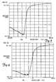
- Figure 2illustrates transfer characteristics of polysilicon TFT after plasma hydrogenation
- Figure 3illustrates transfer characteristics of polysilicon TFT after plasma hydrogenation and plasma deposited SiN x .
- the leakage currentwas improved by a factor of 10 when adding the silicon nitride layer from 8 x 10 -12 A down to 1 X 10 -13 A.
- the sensitivity of the polysilicon TFTswas increased from 5-8 ⁇ A/volt to 30-35 ⁇ A/volt.
- Polysilicon TFTs produced by the technique described in Example 1were bonded to a-Si:H photodiodes in a 1 x 32 array configuration to produce a hybrid structure.
- Approximately 3000 x 10 -10 m (3,000A ⁇ ) of silicon nitridewas coated using plasma enhanced chemical vapor deposition under the same conditions as described in Example 1.
- the nitride coatingwas then followed by approximately 3000 x 10 -10 m (3,000A ⁇ ) of E-beam deposition of aluminum for formation of a contact pad for contacting the a-Si:H photodiodes.
- the addition of the silicon nitride layerimproved the leakage current from 5 x 10 -12 A to 2 x 10 -13 A.
- the sensitivity of the polysilicon TFTwas increased from 8 ⁇ A with plasma hydrogenation to 37 ⁇ A with plasma hydrogenation and silicon nitride layer.
- Example 2Using the technique described in Example 1 to produce polysilicon TFTs in a photodiode/TFTs solid state radiation detector, measurements were taken after the step of depositing the amorphous silicon photodiode array to complete the radiation detector. In this detector, amorphous silicon photodiode array was stacked on top of the polysilicon TFTS. A leakage current of 84 ⁇ /volt in TFTs was found. This improved leakage current indicates that fabrication steps in producing the amorphous silicon photodiodes did not degrade the performance of TFTS. It is believed that such an improved result is due to the deposition temperatures used to produce all the layers of the amorphous silicon photodiodes, the temperatures being below 300°C, which is low enough not to drive out hydrogen.
Landscapes
- Engineering & Computer Science (AREA)
- Physics & Mathematics (AREA)
- Plasma & Fusion (AREA)
- Condensed Matter Physics & Semiconductors (AREA)
- General Physics & Mathematics (AREA)
- Manufacturing & Machinery (AREA)
- Computer Hardware Design (AREA)
- Microelectronics & Electronic Packaging (AREA)
- Power Engineering (AREA)
- Thin Film Transistor (AREA)
- Formation Of Insulating Films (AREA)
- Recrystallisation Techniques (AREA)
Abstract
Description
- The present invention relates to a process for making a polysilicon thinfilm transistor, and in particular, it relates to thosethin film transistors that are suitable for use infabricating radiation sensors and flat panel displays.
- Field Effect Thin Film Transistors (TFTs)fabricated from polysilicon are becoming important due totheir potential for use in sensors and flat panel displays.Polysilicon is becoming a material of choice since TFTsfabricated from polysilicon offer high mobility and stableoperation.
- However, grain boundaries in polysilicon TFTsexert considerable influence on TFT characteristics such asdegradation of carrier transport. Polysilicon TFTs have ananomalous leakage current which decreases the ON/OFFcurrent ratio of the drain current. One source of leakagecurrent is the leakage current produced by grain-boundarydefects. Trap states at the grain boundaries result in alocalized potential barrier being formed for passage ofcarriers from grain to grain. Therefore, reducing the trapstate density becomes increasingly important since it hasbeen suggested that decreasing the grain boundary trapstate density can reduce the leakage current and enhancemobility.
- Hydrogen passivation is one known method forreducing grain boundary trap density and improving theperformance of polysilicon TFTs. Kamins et al,"Hydrogenation of Transistors Fabricated inPolycrystalline-Silicon Films",IEEE Electron DeviceLetters, Volume EDL-1, No. 8, pgs. 159-161 (August 1980)discussed the effect of subjecting a completed polysiliconthin film transistor to a hydrogen-nitrogen plasma in aplanar plasma reactor. The plasma creates an activespecies of hydrogen which can then migrate into thepolysilicon film, passivating the grain boundary states.After hydrogenation, field effect mobility increased bymore than a factor of 10 from 2.6 to 34 cm2/V-sec. Proano et al, "Fabrication and Properties of Single, Double, andTriple Gate Polycrystalline-Silicon Thin Film Transistors",Proc. of Materials Research Society Symposium, Vol. 106,pgs. 317-322 (1988), discussed the effect of plasmahydrogenation of polysilicon TFTS. The hydrogenation wasperformed in a hydrogen-nitrogen atmosphere at 300°C for upto 30 minutes. It was found that drain-source OFF currentwas reduced from 5 x 10⁻¹⁰A to 1 x 10-12A.
- Takashi et al, "High-Performance Poly-Si TFT'sWith ECR-Plasma Hydrogen Passivation",IEEE Transactions onElectron Devices, Vol. 36, No. 3, pgs. 529-553 (March1989), describe hydrogenation carried out in an electroncyclotron resonance reactor on polysilicon TFTs. A smallgrain polysilicon film (average grain size approximately40 nm) was deposited on a quartz substrate at a thicknessof 0.3µm by low pressure chemical vapor deposition at625°C. Recrystallization using CW-Ar laser annealing wasperformed on the polysilicon film to obtain large grains.A standard MOS transistor fabrication process was used toform the polysilicon TFTs. Gate oxide film was obtained bythermal-oxidation of polysilicon at 1,000°C in dry oxygenwith a thickness of the oxide film at 0.1µm. At the gateelectrode, a 0.3µm thick polysilicon layer was deposited bylow pressure chemical vapor deposition and patterned.After deposition of the polysilicon layer, the source anddrain regions were opened. A phosphosilicate glass (PSG)was deposited and annealed at 900°C for one hour innitrogen to form n+regions. The PSG film was removed andaluminum film deposited and patterned. The TFTs were thenannealed in a hydrogen atmosphere at 400°C. The TFTs weretreated in a hydrogen plasma with ECR-plasma apparatus at300°C. A magnetron was used to generate microwaves at afrequency of 2.5 GHz through a rectangular wave guide intothe plasma chamber. Argon was introduced into the plasmachamber at 15 sccm and hydrogen was introduced into thespecimen chamber also at 15 sccm. Treatment was performedat 600 W for 30 minutes. After annealing, the carriermobility was found to have increased from 33.7 cm2/V. sec.to 151.0 cm2/V. sec. It was also observed that the leakage current of the ECR hydrogen plasma treated TFTs was lowerthan that in the TFT without hydrogen passivation.
- Pollack et al, "Hydrogen Passivation ofPolysilicon MOSFET's From a Plasma Nitride Source",IEEEElectron Device Letters, Vol. EDL-5, No. 11, pgs. 468-470(November 1984) studied the effects of hydrogen passivationof polysilicon TFTs using a plasma silicon nitride source.The hydrogen passivation was performed as an extra stepwith the hydrogen from silicon nitride source being driveninto the polysilicon by annealing in nitrogen at 450°C. Asilicon nitride layer was plasma deposited on thepolysilicon TFT. The silicon nitride layer has sufficienthydrogen, typically greater than 1022cm-3, such that thelayer constitutes an ideal diffusion source for atomichydrogen. Annealing was performed at 450°C to hydrogenpassivate the polysilicon grain boundaries.
- Faughnan et al, "A Study of Hydrogen Passivationof Grain Boundaries and Polysilicon Thin Transistors",IEEETransactions on Electron Devices, Vol. 36, No. 1, pgs.101-107 (January 1989) discussed the effect of hydrogenpassivation of grain boundaries on the leakage current ofpolycrystalline silicon thin-film transistors. Hydrogenpassivation was carried out either by annealing the TFTs ina forming gas (5% hydrogen + 95% ammonia) at 600°C, 700°C,and 800°C, or by annealing in ammonia gas at 800°C followedby depositing a 60 nm layer of silicon nitride. Somewafers received further annealing in the forming gas at500°C. No further heat treatment was performed after thepassivation step. Leakage current was found to be reducedbut it was thought that the silicon nitride layer was toothin to play a role. It should be noted that the siliconnitride that was deposited in the study by Faughnan et alwas deposited at 800°C. At such a high temperature,hydrogen tends to be driven out of the deposited layermaking the silicon nitride layer not a good hydrogensource.
- The Meakin et al U.S. Patent 4,880,753 describesa process for manufacturing a polysilicon TFT. The Troxellet al U.S. Patent 4,851,363, the Nakagawa et al U.S. Patent 4,766,477, the Pennell et al U.S. Patent 4,751,196, and theJapanese published application 61-046069 describe the useof silicon nitride layers as insulating layers or surfaceprotective layers against oxidation or moisture in TFTS.
- In each of the above-mentioned examplesoptimizing the conditions to produce consistently highquality polysilicon TFTs has been difficult. For example,in hydrogen passivation of grain boundaries using an atomichydrogen-containing layer such as silicon nitride films,the properties of the film are critical for obtainingeffective and consistent hydrogen passivation of the grainboundaries. Furthermore, diffusion of the hydrogen fromthe silicon nitride layer occurs at deposition temperaturesabove 500°C. See for instance Fritzsche, "Heterogeneitiesand Surface Effects in Glow Discharge DepositedHydrogenated Amorphous Silicon Films",Thin Solid Films,Vol. 90, pgs. 119-129 (1982) ; Biegelsen et al, "HydrogenEvolution and Defect Creation in Amorphous Si:H Alloys",Phvsical Review B, Vol. 20, No. 12, pgs. 4839-4846(December 15, 1979).
- The present invention includes a process for makinga hydrogenated polysilicon thin film transistor asclaimed in claim 1 herein.
- Figure 1 is a schematic diagram of a thin filmtransistor used in the present invention.
- Figure 2 is a graphical view illustrating thetransfer characteristics of a polysilicon TFT after plasmahydrogenation.
- Figure 3 is a graphical view illustrating thetransfer characteristics of a TFT manufactured according to the present invention after plasma hydrogenation and plasma deposited siliconnitride.
- Figure 4 is a graphical view illustrating thetransfer characteristics of polysilicon TFT after plasmahydrogenation and deposition of a silicon nitride layer ofthe present invention with the TFT being incorporated withan amorphous silicon diode array forming a completedintegrated detector.
- The process of the present invention produces apolysilicon thin film transistor (TFT) with very lowleakage currents and high sensitivity that is suitable foruse in solid state radiation sensors, and particularlysensors designed for imaging and medical radiography. Themethod of the present invention provides for hydrogenpassivation of polysilicon grain boundaries in areproducible manner that is much easier to control and ismuch more production oriented than the methods of the priorart.
- By using both hydrogenation and plasmadeposition of a layer of an atomic hydrogen containingsubstance, more consistent hydrogen passivation of thepolysilicon is achieved, along with a leakage current aslow as 10-13A. The hydrogenation preceeds thedeposition of the layer of the atomichydrogen-containing substance. Hydrogenation may be achieved by plasma hydrogenation or by ion implantation techniques. The hydrogen-containingsubstance includes substances such as silicon nitride,silicon oxide, silicon oxide nitride, and silicon carbide,which are deposited in the final stages of fabricating theTFT. Other substances than those listed are alsoincludable within the present invention as long as thesubstance is a good hydrogen source that is the substancecontains 1019 to 1022 atoms/cm3. It is believed that a goodhydrogen source further reduces the trap state density ofthe grain boundaries of the polysilicon and thereforereduces the leakage current of the polysilicon TFT.
- A preferred substance is hydrogenated siliconnitride. The hydrogenation can be carried out by eitherhydrogen ion implantation or by plasma deposition. Such a procedure has the advantage that a final annealingstep is not needed.
- A schematic diagram of the structure of apolysilicon TFT formed by the process of the present invention is generallyindicated at 10 in Figure 1. A substrate such as a single
crystal silicon wafer 12 is coated with a thininsulatinglayer 14 of silicon dioxide at approximately 1 µm usingthermal oxidation techniques. - An undoped
amorphous silicon film 16 ofapproximately 1500 x 10-10m (1,500A ˙) is deposited at 550°C on thesilicondioxide layer 14 by low pressure chemical vapor deposition(LPCVD). The silicon coated wafer is then annealedtypically at 620°C in nitrogen for approximately 24 to 36hours to form a polysilicon film with a grain size in therange of 600 x 10-10 to 5000 x 10-10m (600A ˙ to 5,000A ˙). Amorphous silicon film can alsobe made at 200°C to 300°C using plasma-enhanced chemicalvapor deposition (PECVD). The film is then annealed in afurnace at 620°C for 24 to 36 hours or by rapid thermalannealing for 5 to 20 minutes to form polysilicon film. Asan option, E-beam annealing can also be used to formpolysilicon film. - The
polysilicon film 16 is then patterned intoislands. Asilicon dioxide layer 18 used as the gatedielectric is thermally grown on the polysiliconthin layer 16 to a thickness of approximately 1000 x 10-10m (1,000A ˙). - A
polysilicon layer 28 of approximately 3500 x 10-10m (3,500A ˙)thick is then deposited on thelayer 16 by LPCVD. Thelayer 28 is then patterned and asource area 20,drain area 22, and polysilicon gate are doped with phosphorous to alevel of approximately 1015/cm2 to obtain n-typecharacteristics, using ion implantation technique. - Contact holes are etched through the oxide overthe source and drain
areas source contact 24, adrain contact 26, andgate contact 30for the respective source and drain and gate areas using alift-off procedure. The aluminum is later used as a blocking mask for reactive ion etching of a subsequentlyapplied silicon nitride layer. - The now formed TFT is annealed at approximately400°C in a forming gas of hydrogen and nitrogen at a ratioof 15:85. The annealing step is common practice in the artto improve the aluminum contact of the drain, source, andgate electrodes.
- Hydrogen plasma hydrogenation is then performedat a temperature in the approximate range of 150°C to400°C, preferably at a temperature of approximately 300°C,for a time in the range of 30 minutes to 4 hours. A radiofrequency power density in the range of 0.5W/cm2 to 20W/cm2is used. The reactant gas may be hydrogen or a mixture ofhydrogen with nitrogen or with inert gases such as argonand helium. Alternatively, the plasma hydrogenation may becarried out in an electron cyclotron resonance chemicalvapor deposition system (ECRCVD).
- The deposition of the atomic hydrogen containinglayer may be performed by plasma enhanced chemical vapordeposition of for example, silicon nitride. The plasmapower is derived either from a radio frequency supply orfrom electron cyclotron resonance. A suitable atomichydroyen-containing layer is of a thickness in the range of1000 x 10-10 to 5000 x 10-10m (1,000A ˙ to 5,0000A ˙) deposited from a silane/ammonia/nitrogengas mixture at a pressure of approximately 133 Pa (1 Torr) and atemperature in the range of approximately 150°C to 450°C,preferably in the range of 200°C to 400°C.
- The hydrogenated silicon nitride layer acts ashigh concentration diffusion source of atomic hydrogen.Other substances suitable for the atomic hydrogen -containing layer include silicon oxide, silicon carbide,combinations of silicon nitride and silicon oxide, siliconoxide nitride, and other silicon based layers.
- The plasma hydrogenation and the succeedingdeposition of the atomic hydrogen-containing layer may becarried out in one vacuum pumpdown or may separated intotwo vacuum pumpdowns with any interim time period atatmospheric pressure in between the pumpdowns. As caneasily be understood, such a procedure provides great latitude in production techniques of the TFT of the presentinvention.
- Polysilicon used in the present invention can bemade at a temperature in the range of 550°C to 620°C.Silicon fabricated at or below 550°C is amorphous, but canbe transformed into polysilicon by annealing at 620°C for aperiod of time in the range of 24 to 36 hours, or by rapidthermal annealing, E-beam annealing or by laser annealing.As discussed previously above, the substrate used was asilicon wafer. However, a quartz substrate can also beused and when the process temperature is reduced below800°C, a glass substrate is also a good candidate.
- The improved polysilicon TFTs formed by the process of the presentinvention that have been hydrogen passivated, have aleakage current of approximately 10-13A. Sensitivity wasmeasured in the range of 5-40µA/volt, and a preferred rangeof 30-38µA/volt shows improvement by a factor in the rangeof 5 to 8 over the sensitivity of plasma hydrogenatedpolysilicon TFTs before SiNx coating. The ON (maximum)/OFF(minimum) current ratio was found to be 109.
- The following examples are for illustrativepurposes and are not to be considered as limiting thepresent invention.
- A one micrometer layer of silicon oxide was grown forinsulation on three-inch silicon wafers. Next, undopedpolysilicon film of approximately 1500 x 10-10m (1,500A ˙) thick wasdeposited at 560°C with SIH4 at 21.33 Pa (160mTorr) and 28 sccm, usinglow pressure chemical vapor deposition (LPCVD). The waferswere then annealed in a nitrogen atmosphere ofapproximately 200 Pa (1.5 Torr) at 620°C for 24 hours. Theresulting grain size of the polysilicon film wasapproximately 500 x 10-10 to 700 x 10-10m (500A ˙ to 700A ˙). The polysilicon film was thenpatterned into islands using microlithographic methods, andapproximately 1000 x 10-10m (1,000A ˙) gate oxide was thermally grown on thepolysilicon film at approximately 1,150°C in an oxygenatmosphere. A polysilicon layer of approximately 3500 x 10-10m (3,500A ˙)thick was then deposited using LPCVD for the gate andpatterned with deposition conditions of 28 sccm, 23.998 Pa (180mTorr) at 620°C. 1015/cm2 phosphorous was implanted to dope thesource, drain, and gate areas. The dopant was activatedduring a 30 minute nitrogen annealing step at approximately1,050°C.
- Contact holes were then etched through the gateoxide over the source and drain and aluminum deposited forcontacts using a lift-off procedure. Aluminum was alsodeposited as a contact for the gate electrode which is alsosubsequently used as a blocking mask for the reactive ionetching of the subsequently formed silicon nitride layer.
- The now formed TFT was then annealed in a forminggas of approximately 15% hydrogen and 85% nitrogen at 400°Cfor 30 minutes. After annealing, the TFT was hydrogenatedin a hydrogen plasma of approximately 50% hydrogen at 50%nitrogen under a total pressure of 73.3 Pa (550mTorr) for 30 minutesat 300°C using a power density of 1.15W/cm The hydrogenateddevices were then coated with 3000 x 10-10m (3,000A ˙) of silicon nitrideusing plasma enhanced chemical vapor deposition and thenpatterned using reactive ion etching. In the deposition,the SiH4/N2 ratio was 1/7, and the NH3/N2 ratio was 1/4. Thetotal pressure used was 1 Torr, and the power density was0.35W/cm2 at a temperature of 300°C.
- Figure 2 illustrates transfer characteristics ofpolysilicon TFT after plasma hydrogenation while Figure 3illustrates transfer characteristics of polysilicon TFTafter plasma hydrogenation and plasma deposited SiNx. As canbe seen by comparing Figures 2 and 3, it was discoveredthat the leakage current was improved by a factor of 10when adding the silicon nitride layer from 8 x 10-12A down to1
X 10-13A. Also the sensitivity of the polysilicon TFTs wasincreased from 5-8µA/volt to 30-35µA/volt. - Polysilicon TFTs produced by the techniquedescribed in Example 1 were bonded to a-Si:H photodiodes ina 1 x 32 array configuration to produce a hybrid structure.Approximately 3000 x 10-10m (3,000A ˙) of silicon nitride was coated usingplasma enhanced chemical vapor deposition under the sameconditions as described in Example 1. The nitridecoating was then followed by approximately 3000 x 10-10m (3,000A ˙) of E-beam deposition of aluminum for formation of a contact pad forcontacting the a-Si:H photodiodes. The addition of thesilicon nitride layer improved the leakage current from 5 x10-12A to 2 x 10-13A. In addition, the sensitivity of thepolysilicon TFT was increased from 8µA with plasmahydrogenation to 37µA with plasma hydrogenation and siliconnitride layer.
- Using the technique described in Example 1 toproduce polysilicon TFTs in a photodiode/TFTs solid stateradiation detector, measurements were taken after the stepof depositing the amorphous silicon photodiode array tocomplete the radiation detector. In this detector,amorphous silicon photodiode array was stacked on top ofthe polysilicon TFTS. A leakage current of 84µ/volt inTFTs was found. This improved leakage current indicatesthat fabrication steps in producing the amorphous siliconphotodiodes did not degrade the performance of TFTS. It isbelieved that such an improved result is due to thedeposition temperatures used to produce all the layers ofthe amorphous silicon photodiodes, the temperatures beingbelow 300°C, which is low enough not to drive out hydrogen.
Claims (6)
- A process for making a hydrogenated polysilicon thinfilm transistor comprising the steps of:providing a substrate (12);depositing a layer of amorphous silicon (16) on thesubstrate;annealing the layer of amorphous silicon to form afirst polysilicon layer (16);patterning the first polysilicon layer (16) to formislands;growing a layer of silicon dioxide (18) on theislands to form a gate dielectric layer;depositing and patterning a second layer (28) ofpolysilicon;doping the first and second polysilicon layers toform a source (20), a drain (22), and a gate (28);depositing and patterning a metal layer to provide asource contact (24), a drain contact (26), and a gatecontact (30) for the respective source, drain, and gateand thereby forming a polysilicon thin film transistor;annealing the polysilicon thin film transistor; andhydrogenating the polysilicon thin film transistorprior to depositing an atomic hydrogen-containing layeron the polysilicon thin film transistor, wherein theatomic hydrogen-containing layer contains 1019 to 1022atoms per cubic centimeter of hydrogen.
- The process of claim 1, wherein the atomichydrogen-containing layer includes a hydrogenated form of asilicon compound.
- The process of claim 2, wherein the siliconcompound is selected from the group consisting of siliconoxide, silicon nitride, silicon carbide, and silicon oxidenitride.
- The process of claim 1, wherein the hydrogenatingstep includes plasma hydrogenation.
- The process of claim 1, wherein the hydrogenationincludes ion implantation.
- The process of claim 1, wherein the hydrogen-containinglayer is formed at a temperature in theapproximate range of 150°C to 450°C.
Applications Claiming Priority (3)
| Application Number | Priority Date | Filing Date | Title |
|---|---|---|---|
| US64852991A | 1991-01-30 | 1991-01-30 | |
| PCT/US1992/000210WO1992014268A1 (en) | 1991-01-30 | 1992-01-08 | Polysilicon thin film transistor |
| US648529 | 2000-08-22 |
Publications (2)
| Publication Number | Publication Date |
|---|---|
| EP0569470A1 EP0569470A1 (en) | 1993-11-18 |
| EP0569470B1true EP0569470B1 (en) | 1999-04-07 |
Family
ID=24601152
Family Applications (1)
| Application Number | Title | Priority Date | Filing Date |
|---|---|---|---|
| EP92904576AExpired - LifetimeEP0569470B1 (en) | 1991-01-30 | 1992-01-08 | Process for making a polysilicon thin film transistor |
Country Status (8)
| Country | Link |
|---|---|
| US (1) | US5534445A (en) |
| EP (1) | EP0569470B1 (en) |
| JP (1) | JPH06505362A (en) |
| KR (1) | KR930703707A (en) |
| CA (1) | CA2100065A1 (en) |
| DE (1) | DE69228868D1 (en) |
| MX (1) | MX9200257A (en) |
| WO (1) | WO1992014268A1 (en) |
Families Citing this family (35)
| Publication number | Priority date | Publication date | Assignee | Title |
|---|---|---|---|---|
| US5719065A (en) | 1993-10-01 | 1998-02-17 | Semiconductor Energy Laboratory Co., Ltd. | Method for manufacturing semiconductor device with removable spacers |
| JP2738315B2 (en)* | 1994-11-22 | 1998-04-08 | 日本電気株式会社 | Thin film transistor and method of manufacturing the same |
| US6933182B1 (en) | 1995-04-20 | 2005-08-23 | Semiconductor Energy Laboratory Co., Ltd. | Method of manufacturing a semiconductor device and manufacturing system thereof |
| US6444506B1 (en)* | 1995-10-25 | 2002-09-03 | Semiconductor Energy Laboratory Co., Ltd. | Method of manufacturing silicon thin film devices using laser annealing in a hydrogen mixture gas followed by nitride formation |
| US5808318A (en)* | 1996-03-03 | 1998-09-15 | Ag Technology Co., Ltd. | Polycrystalline semiconductor thin film for semiconductor TFT on a substrate having a mobility in a longitudinal direction greater than in a width direction |
| US5744202A (en)* | 1996-09-30 | 1998-04-28 | Xerox Corporation | Enhancement of hydrogenation of materials encapsulated by an oxide |
| US5707895A (en)* | 1996-10-21 | 1998-01-13 | Taiwan Semiconductor Manufacturing Company, Ltd. | Thin film transistor performance enhancement by water plasma treatment |
| TW386238B (en)* | 1997-01-20 | 2000-04-01 | Semiconductor Energy Lab | Semiconductor device and method of manufacturing the same |
| JP4401448B2 (en)* | 1997-02-24 | 2010-01-20 | 株式会社半導体エネルギー研究所 | Method for manufacturing semiconductor device |
| JPH10275913A (en)* | 1997-03-28 | 1998-10-13 | Sanyo Electric Co Ltd | Semiconductor device, method of manufacturing semiconductor device, and method of manufacturing thin film transistor |
| US6057182A (en)* | 1997-09-05 | 2000-05-02 | Sarnoff Corporation | Hydrogenation of polysilicon thin film transistors |
| JP3599972B2 (en)* | 1997-09-30 | 2004-12-08 | 三洋電機株式会社 | Method for manufacturing thin film transistor |
| JPH11111991A (en) | 1997-09-30 | 1999-04-23 | Sanyo Electric Co Ltd | Thin film transistor and method of manufacturing thin film transistor |
| JPH11111994A (en)* | 1997-10-03 | 1999-04-23 | Sanyo Electric Co Ltd | Thin film transistor and method of manufacturing thin film transistor |
| JPH11111998A (en) | 1997-10-06 | 1999-04-23 | Sanyo Electric Co Ltd | Method for manufacturing thin film transistor |
| US7053002B2 (en)* | 1998-12-04 | 2006-05-30 | Applied Materials, Inc | Plasma preclean with argon, helium, and hydrogen gases |
| KR100390822B1 (en)* | 1999-12-28 | 2003-07-10 | 주식회사 하이닉스반도체 | Method for reducing dark current in image sensor |
| JP2001313384A (en)* | 2000-04-28 | 2001-11-09 | Shimadzu Corp | Radiation detector |
| GB0017471D0 (en)* | 2000-07-18 | 2000-08-30 | Koninkl Philips Electronics Nv | Thin film transistors and their manufacture |
| JP2002280550A (en)* | 2001-03-22 | 2002-09-27 | Mitsubishi Electric Corp | Semiconductor device manufacturing method and semiconductor device |
| TW200304227A (en)* | 2002-03-11 | 2003-09-16 | Sanyo Electric Co | Top gate type thin film transistor |
| US7038239B2 (en) | 2002-04-09 | 2006-05-02 | Semiconductor Energy Laboratory Co., Ltd. | Semiconductor element and display device using the same |
| JP3989761B2 (en) | 2002-04-09 | 2007-10-10 | 株式会社半導体エネルギー研究所 | Semiconductor display device |
| US7256421B2 (en) | 2002-05-17 | 2007-08-14 | Semiconductor Energy Laboratory, Co., Ltd. | Display device having a structure for preventing the deterioration of a light emitting device |
| NL1020634C2 (en)* | 2002-05-21 | 2003-11-24 | Otb Group Bv | Method for passivating a semiconductor substrate. |
| GB0222450D0 (en)* | 2002-09-27 | 2002-11-06 | Koninkl Philips Electronics Nv | Method of manufacturing an electronic device comprising a thin film transistor |
| US6841431B2 (en)* | 2003-01-29 | 2005-01-11 | Chunghwa Picture Tubes, Ltd. | Method for reducing the contact resistance |
| TWI221320B (en)* | 2003-05-08 | 2004-09-21 | Toppoly Optoelectronics Corp | Process for passivating polysilicon and process for fabricating polysilicon thin film transistor |
| US7507618B2 (en)* | 2005-06-27 | 2009-03-24 | 3M Innovative Properties Company | Method for making electronic devices using metal oxide nanoparticles |
| JP3986544B2 (en)* | 2006-12-11 | 2007-10-03 | 株式会社半導体エネルギー研究所 | Semiconductor fabrication method |
| US8861909B2 (en) | 2011-02-17 | 2014-10-14 | Cornell University | Polysilicon photodetector, methods and applications |
| CN105940498B (en) | 2014-03-11 | 2019-12-10 | 富士电机株式会社 | Method for manufacturing silicon carbide semiconductor device and silicon carbide semiconductor device |
| CN103985637B (en)* | 2014-04-30 | 2017-02-01 | 京东方科技集团股份有限公司 | Low-temperature polycrystalline silicon thin film transistor, manufacturing method thereof and display device |
| US9793252B2 (en) | 2015-03-30 | 2017-10-17 | Emagin Corporation | Method of integrating inorganic light emitting diode with oxide thin film transistor for display applications |
| US10490689B1 (en)* | 2018-01-31 | 2019-11-26 | Hrl Laboratories, Llc | Grain boundary passivation of polycrystalline materials |
Family Cites Families (21)
| Publication number | Priority date | Publication date | Assignee | Title |
|---|---|---|---|---|
| US4226898A (en)* | 1978-03-16 | 1980-10-07 | Energy Conversion Devices, Inc. | Amorphous semiconductors equivalent to crystalline semiconductors produced by a glow discharge process |
| JPH0658966B2 (en)* | 1982-05-17 | 1994-08-03 | キヤノン株式会社 | Semiconductor element |
| JPS6016462A (en)* | 1983-07-08 | 1985-01-28 | Seiko Epson Corp | Manufacturing method of semiconductor device |
| CA1218470A (en)* | 1983-12-24 | 1987-02-24 | Hisayoshi Yamoto | Semiconductor device with polycrystalline silicon active region and ic including semiconductor device |
| US4769338A (en)* | 1984-05-14 | 1988-09-06 | Energy Conversion Devices, Inc. | Thin film field effect transistor and method of making same |
| JPH0656856B2 (en)* | 1984-08-10 | 1994-07-27 | ソニー株式会社 | Method for manufacturing semiconductor device |
| US4751196A (en)* | 1985-04-01 | 1988-06-14 | Motorola Inc. | High voltage thin film transistor on PLZT and method of manufacture thereof |
| JPS6251264A (en)* | 1985-08-30 | 1987-03-05 | Hitachi Ltd | Manufcture of thin film transistor |
| US4851363A (en)* | 1986-07-11 | 1989-07-25 | General Motors Corporation | Fabrication of polysilicon fets on alkaline earth alumino-silicate glasses |
| JPH0752772B2 (en)* | 1986-11-22 | 1995-06-05 | ヤマハ株式会社 | Manufacturing method of semiconductor device |
| JPH0687503B2 (en)* | 1987-03-11 | 1994-11-02 | 株式会社日立製作所 | Thin film semiconductor device |
| JP2764395B2 (en)* | 1987-04-20 | 1998-06-11 | セイコーエプソン株式会社 | Method for manufacturing thin film transistor |
| JPH0640550B2 (en)* | 1987-06-09 | 1994-05-25 | 沖電気工業株式会社 | Method of manufacturing thin film transistor |
| US4857976A (en)* | 1987-06-30 | 1989-08-15 | California Institute Of Technology | Hydrogen-stabilized semiconductor devices |
| JPS6461062A (en)* | 1987-09-01 | 1989-03-08 | Ricoh Kk | Manufacture of thin film transistor |
| JP2589327B2 (en)* | 1987-11-14 | 1997-03-12 | 株式会社リコー | Method for manufacturing thin film transistor |
| GB2215126B (en)* | 1988-02-19 | 1990-11-14 | Gen Electric Co Plc | Process for manufacturing a thin film transistor |
| JPH01275745A (en)* | 1988-04-27 | 1989-11-06 | Tosoh Corp | Silicon nitride thin film and its manufacturing method |
| JP3055782B2 (en)* | 1988-09-19 | 2000-06-26 | セイコーエプソン株式会社 | How to manufacture thin film transistors |
| EP0383230B1 (en)* | 1989-02-14 | 1997-05-28 | Seiko Epson Corporation | Manufacturing Method of a Semiconductor Device |
| US5273910A (en)* | 1990-08-08 | 1993-12-28 | Minnesota Mining And Manufacturing Company | Method of making a solid state electromagnetic radiation detector |
- 1992
- 1992-01-08CACA002100065Apatent/CA2100065A1/ennot_activeAbandoned
- 1992-01-08WOPCT/US1992/000210patent/WO1992014268A1/enactiveIP Right Grant
- 1992-01-08KRKR1019930702249Apatent/KR930703707A/ennot_activeAbandoned
- 1992-01-08EPEP92904576Apatent/EP0569470B1/ennot_activeExpired - Lifetime
- 1992-01-08DEDE69228868Tpatent/DE69228868D1/ennot_activeExpired - Lifetime
- 1992-01-08JPJP4504511Apatent/JPH06505362A/enactivePending
- 1992-01-21MXMX9200257Apatent/MX9200257A/ennot_activeIP Right Cessation
- 1995
- 1995-05-23USUS08/447,926patent/US5534445A/ennot_activeExpired - Fee Related
Non-Patent Citations (2)
| Title |
|---|
| IEEE Electron Device Letters, vol. EDL-5, no. 11, November 1984, pages 468-470* |
| IEEE Transactions on Electron Devices, vol. 36, no. 1, January 1989, pages 101-107* |
Also Published As
| Publication number | Publication date |
|---|---|
| US5534445A (en) | 1996-07-09 |
| MX9200257A (en) | 1992-10-01 |
| JPH06505362A (en) | 1994-06-16 |
| CA2100065A1 (en) | 1992-07-31 |
| KR930703707A (en) | 1993-11-30 |
| DE69228868D1 (en) | 1999-05-12 |
| EP0569470A1 (en) | 1993-11-18 |
| WO1992014268A1 (en) | 1992-08-20 |
Similar Documents
| Publication | Publication Date | Title |
|---|---|---|
| EP0569470B1 (en) | Process for making a polysilicon thin film transistor | |
| US5817549A (en) | Method for manufacturing a semiconductor device | |
| US8330165B2 (en) | Semiconductor device and method for forming the same | |
| US6423586B1 (en) | Method for crystallizing semiconductor material without exposing it to air | |
| US5962869A (en) | Semiconductor material and method for forming the same and thin film transistor | |
| US6403497B1 (en) | Method of manufacturing semiconductor device by two stage heating of deposited noncrystalline semiconductor | |
| US5744818A (en) | Insulated gate field effect semiconductor device | |
| JPH05299339A (en) | Semiconductor material and manufacturing method thereof | |
| EP0589713B1 (en) | A thin film semiconductor device and a method for producing the same | |
| JPH01187814A (en) | Manufacture of thin film semiconductor device | |
| EP0496639B1 (en) | Polysilicon thin film semiconductor device | |
| US6777354B2 (en) | Semiconductor device and method of manufacturing the same | |
| JPH02148831A (en) | Laser annealing method and thin film semiconductor device | |
| US6150203A (en) | Method for manufacturing a semiconductor device | |
| US6706572B1 (en) | Method for manufacturing a thin film transistor using a high pressure oxidation step | |
| JP3942853B2 (en) | Semiconductor material manufacturing equipment | |
| JP2864623B2 (en) | Method for manufacturing semiconductor device | |
| RU2819702C1 (en) | Method of making a thin-film transistor | |
| JP3986781B2 (en) | Method for manufacturing thin film transistor | |
| JP3987311B2 (en) | Method for manufacturing thin film transistor | |
| JP3987310B2 (en) | Method for producing crystalline silicon film | |
| JP3986772B2 (en) | Method for manufacturing thin film transistor | |
| JP3075498B2 (en) | Method for manufacturing thin film transistor | |
| JP3986771B2 (en) | Method for producing crystalline silicon film | |
| JP3987062B2 (en) | Method for manufacturing thin film transistor |
Legal Events
| Date | Code | Title | Description |
|---|---|---|---|
| PUAI | Public reference made under article 153(3) epc to a published international application that has entered the european phase | Free format text:ORIGINAL CODE: 0009012 | |
| 17P | Request for examination filed | Effective date:19930825 | |
| AK | Designated contracting states | Kind code of ref document:A1 Designated state(s):AT BE CH DE DK ES FR GB GR IT LI LU MC NL SE | |
| RBV | Designated contracting states (corrected) | Designated state(s):CH DE FR GB LI NL | |
| 17Q | First examination report despatched | Effective date:19960216 | |
| GRAG | Despatch of communication of intention to grant | Free format text:ORIGINAL CODE: EPIDOS AGRA | |
| GRAG | Despatch of communication of intention to grant | Free format text:ORIGINAL CODE: EPIDOS AGRA | |
| GRAH | Despatch of communication of intention to grant a patent | Free format text:ORIGINAL CODE: EPIDOS IGRA | |
| GRAH | Despatch of communication of intention to grant a patent | Free format text:ORIGINAL CODE: EPIDOS IGRA | |
| GRAA | (expected) grant | Free format text:ORIGINAL CODE: 0009210 | |
| AK | Designated contracting states | Kind code of ref document:B1 Designated state(s):CH DE FR GB LI NL | |
| PG25 | Lapsed in a contracting state [announced via postgrant information from national office to epo] | Ref country code:NL Free format text:LAPSE BECAUSE OF FAILURE TO SUBMIT A TRANSLATION OF THE DESCRIPTION OR TO PAY THE FEE WITHIN THE PRESCRIBED TIME-LIMIT Effective date:19990407 Ref country code:LI Free format text:LAPSE BECAUSE OF FAILURE TO SUBMIT A TRANSLATION OF THE DESCRIPTION OR TO PAY THE FEE WITHIN THE PRESCRIBED TIME-LIMIT Effective date:19990407 Ref country code:CH Free format text:LAPSE BECAUSE OF FAILURE TO SUBMIT A TRANSLATION OF THE DESCRIPTION OR TO PAY THE FEE WITHIN THE PRESCRIBED TIME-LIMIT Effective date:19990407 | |
| REG | Reference to a national code | Ref country code:CH Ref legal event code:EP | |
| REF | Corresponds to: | Ref document number:69228868 Country of ref document:DE Date of ref document:19990512 | |
| ET | Fr: translation filed | ||
| PG25 | Lapsed in a contracting state [announced via postgrant information from national office to epo] | Ref country code:DE Free format text:LAPSE BECAUSE OF FAILURE TO SUBMIT A TRANSLATION OF THE DESCRIPTION OR TO PAY THE FEE WITHIN THE PRESCRIBED TIME-LIMIT Effective date:19990708 | |
| NLV1 | Nl: lapsed or annulled due to failure to fulfill the requirements of art. 29p and 29m of the patents act | ||
| REG | Reference to a national code | Ref country code:CH Ref legal event code:PL | |
| PG25 | Lapsed in a contracting state [announced via postgrant information from national office to epo] | Ref country code:GB Free format text:LAPSE BECAUSE OF NON-PAYMENT OF DUE FEES Effective date:20000108 | |
| PLBE | No opposition filed within time limit | Free format text:ORIGINAL CODE: 0009261 | |
| STAA | Information on the status of an ep patent application or granted ep patent | Free format text:STATUS: NO OPPOSITION FILED WITHIN TIME LIMIT | |
| 26N | No opposition filed | ||
| GBPC | Gb: european patent ceased through non-payment of renewal fee | Effective date:20000108 | |
| PG25 | Lapsed in a contracting state [announced via postgrant information from national office to epo] | Ref country code:FR Free format text:LAPSE BECAUSE OF NON-PAYMENT OF DUE FEES Effective date:20010928 | |
| REG | Reference to a national code | Ref country code:FR Ref legal event code:ST | |
| PG25 | Lapsed in a contracting state [announced via postgrant information from national office to epo] | Ref country code:FR Free format text:LAPSE BECAUSE OF NON-PAYMENT OF DUE FEES Effective date:20000131 |