EP0569218B1 - Circuit for rotating a ditigal image - Google Patents
Circuit for rotating a ditigal imageDownload PDFInfo
- Publication number
- EP0569218B1 EP0569218B1EP93303466AEP93303466AEP0569218B1EP 0569218 B1EP0569218 B1EP 0569218B1EP 93303466 AEP93303466 AEP 93303466AEP 93303466 AEP93303466 AEP 93303466AEP 0569218 B1EP0569218 B1EP 0569218B1
- Authority
- EP
- European Patent Office
- Prior art keywords
- lines
- significant
- image
- bits
- counter
- Prior art date
- Legal status (The legal status is an assumption and is not a legal conclusion. Google has not performed a legal analysis and makes no representation as to the accuracy of the status listed.)
- Expired - Lifetime
Links
Images


Classifications
- G—PHYSICS
- G06—COMPUTING OR CALCULATING; COUNTING
- G06T—IMAGE DATA PROCESSING OR GENERATION, IN GENERAL
- G06T3/00—Geometric image transformations in the plane of the image
- G06T3/60—Rotation of whole images or parts thereof
- G06T3/606—Rotation of whole images or parts thereof by memory addressing or mapping
- G—PHYSICS
- G11—INFORMATION STORAGE
- G11C—STATIC STORES
- G11C7/00—Arrangements for writing information into, or reading information out from, a digital store
- G11C7/10—Input/output [I/O] data interface arrangements, e.g. I/O data control circuits, I/O data buffers
- G11C7/1015—Read-write modes for single port memories, i.e. having either a random port or a serial port
- G11C7/1018—Serial bit line access mode, e.g. using bit line address shift registers, bit line address counters, bit line burst counters
- G11C7/1021—Page serial bit line access mode, i.e. using an enabled row address stroke pulse with its associated word line address and a sequence of enabled column address stroke pulses each with its associated bit line address
Definitions
- the present inventionrelates to a circuit for addressing a random access memory device having x address lines divided into column address lines and row address lines according to the preamble part of claim 1.
- each line of each block of the imageis circularly shifted by the line number within the block and then stored in a buffer memory.
- line 0is circularly shifted 0 bits
- line 1is circularly shifted 1 bit, etc.
- the imagecan either be read out of the buffer and not rotated at all, or read out in such a way that the final image is rotated by any multiple of 90 degrees, including all mirror images.
- the imageis read out one line at a time, and is simply shifted back to its original form.
- the image blockis read out from the buffer along diagonal lines, and circularly shifted again.
- the fast page modeWhen reading in image data to the buffer, the fast page mode can be used. This is a feature designed into memory devices, and provides that the data can be stored or read out at a higher speed provided that the row address does not change from one access to the next. For example, when reading words into a buffer, assume that the data is read into row 0 col 0, row 0 col 1, row 0 col 2, etc. Since the row address does not change, the fast page mode can be used, and the total data transfer can be done in a fraction of the time that it would otherwise take.
- the column addressesneed not be sequential, as long as the row address is constant.
- the procedureis simply the reverse of the loading procedure, and that can also be handled in the fast page mode.
- EP-A-0 276 110discloses a semiconductor memory device with an address scramble unit and a multidirection data selection unit in which a continuous sixteen bit data selection of a raster-type scanning on all of the X-, Y- and S-direction accesses can be made.
- the address scramble unitconverts an external address consisting of an external column address and external row address into an internal directional address consisting of a row address, a segment designation address and a segment internal address.
- a word counterkeeps track of the number of words, and will finally contain the total count of words in the image.
- the least significant half of the counteris used to address the image in the vertical direction and the most significant half of the counter to address the image in the horizontal direction.
- This imageis temporarily stored in a page buffer comprising memory devices having column and row address lines.
- the least significant half of the image counterwhich addresses the image in the vertical direction, is connected to the column address lines of the memory devices, and the most significant half of the image counter, which addresses the image in horizontal direction, to the row address lines of the memory device.
- a preferred embodiment of the present inventionuses the least significant 6 bits of the counter to address the image in the vertical direction and the least significant 5 bits of the counter to address the image in the horizontal direction as column address inputs of the memory devices of the page buffer. Similarly, all of the remaining most significant bits of the addresses for the vertical direction and horizontal direction are connected to the row address lines of the memory devices of the page buffer.
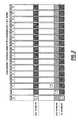
- Each scanlineis made up of 512 words of 16 bits each, for a total of 8K bits, and there are 8K scan lines in the page.
- the first scanlineis shown in black and the second scanline is shown as crosshatched.
- the second scanlineis shown as crosshatched.
- 8K vertical rows and 512 horizontal columns in the imageare then grouped into 16 by 16 bit blocks as shown.
- Fig 2shows how these lines are loaded into a page buffer arranged according to the prior art. Each scan line is shifted if necessary, and then loaded into 512 words of the buffer as shown. The result is one row for each scan line.
- the 8K by 8K bufferis segmented into 16 bit words and there are a total of 4,194,304 words, which requires a 22 bit word counter.
- the least significant 9 lines, C0 through C8count the words in each vertical line of blocks in the image (512), bits C9 - C12 count the row lines within the block (16x16 bit block) and the remaining 9 address lines C13 - C21, count the blocks in the horizontal direction of the image .
- Counter bits, C9-C12are identical in value to the number of bits that the data must be shifted before loading, and therefore are used to control the shifter as well as address the buffer.
- C0 - C8are connected to A0 - A8 of the memory devices and used to address the blocks in the vertical direction
- C13 - C21are connected to A13 - A21 of the memory devices and used to address the blocks in the horizontal direction
- C9 - C12are connected to A9 - A12 and used to address the lines within the 16-blocks and also to control the shifter to shift the data back to its original position.
- Fig 4shows the location of data in page buffer. As shown, the image is divided up into 16 line (in the horizontal direction) by sixteen bit (per word) blocks. For the first block, address lines A0 - A8 and A13 - A21 are all 0. For the second block in the scan line direction, the address lines A0 - A8 equal 1 and the address lines A13 - A21 equal 0. Within the block, individual words are addressed by address lines A9 - A12.
- each entire scan line of 512 wordsis completely read in or out before the next line is started.
- the read-inis identical, but on read-out, the process reads out the same diagonal line from every block in the horizontal line of blocks before going on to the next diagonal line in all of the blocks in the same horizontal line, until all the diagonal lines in the 16-bit block are accessed. Then, the process reads out the diagonal lines from every block in the next set of 16-bit blocks in the horizontal direction. Therefore, for each random access memory (RAM), each consecutive read comes from a different row, and the slow page mode must be used.
- RAMrandom access memory
- the addressing lines A13 - A21 of the memory devices for addressing the 16-bit blocks in the horizontal directionare taken from the counter C0 - C8, and lines A0 - A8 of the memory devices to address the 16-bit blocks in the vertical direction are taken from the counter C13 - C21.
- the address lines A9 - A12 to each RAM deviceare a function of counter bits C9 - C12.
- the processis to read out the same diagonal line, as defined by bits 9 - 12, in each of the 512 blocks in the horizontal direction before going on to the next diagonal line.
- Fig 6is a circuit of the prior art addressing arrangement shown in Figs 3 and 5.
- the memoryis configured as 2K by 2K, which requires 11 address lines for row and column addresses. Therefore, for non-rotated images, bits C0 - C10 are used for column addressing and C11 - 21 are used for the rows.
- the multiplexers 12, 13, as showncouple bits C0 - C8 to address lines A13 - A21 and C13 - C21 to address lines A0 - A8. This effectively switches the read out from along the vertical direction to along the horizontal direction. However, as shown, the central 4 bits remain unchanged. These bits determine the line within the block, and this number does not change whether the read out is along a row or column. As described above, the read out for rotated images is in the horizontal direction (the counter increments the row addresses, A13 - A21, once for each readout), and therefore must proceed at the slow page mode speed.
- Fig 7is the schematic diagram of the present invention.
- the arrangement of the counter 10 and multiplexers 12, 13is identical to that of the prior art.
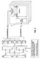
- the column address lines to the RAMare taken from bits A0 - A5 and A13 - A17 of the address line register 11 which are the least significant bits of the row and column counters. Therefore, there can be either 31 or 63 readouts along a row or column in the fast page mode before a slow page mode read out is required.
Landscapes
- Physics & Mathematics (AREA)
- General Physics & Mathematics (AREA)
- Engineering & Computer Science (AREA)
- Theoretical Computer Science (AREA)
- Image Processing (AREA)
- Controls And Circuits For Display Device (AREA)
- Memory System (AREA)
- Editing Of Facsimile Originals (AREA)
- Image Input (AREA)
- Dram (AREA)
Description
- The present invention relates to a circuit for addressing a random access memory device having xaddress lines divided into column address lines and row address lines according to the preamble part of
claim 1. - The basic circuit has been described in EP-A-0,433,645.
- The basic system of rotating a block of an image requires first that each line of each blockof the image is circularly shifted by the line number within the block and then stored in a buffermemory. For example,
line 0 is circularly shifted 0 bits,line 1 is circularly shifted 1 bit, etc. At thispoint the image can either be read out of the buffer and not rotated at all, or read out in such a waythat the final image is rotated by any multiple of 90 degrees, including all mirror images. - To get back the original orientation, the image is read out one line at a time, and is simplyshifted back to its original form. To get a rotated image, the image block is read out from the bufferalong diagonal lines, and circularly shifted again.
- When reading in image data to the buffer, the fast page mode can be used. This is afeature designed into memory devices, and provides that the data can be stored or read out at ahigher speed provided that the row address does not change from one access to the next. Forexample, when reading words into a buffer, assume that the data is read into
row 0col 0,row 0col 1,row 0col 2, etc. Since the row address does not change, the fast page mode can be used, andthe total data transfer can be done in a fraction of the time that it would otherwise take. The columnaddresses need not be sequential, as long as the row address is constant. - Similarly, to take data out of the buffer in non-rotated form, the procedure is simply thereverse of the loading procedure, and that can also be handled in the fast page mode.
- A problem occurs when reading from the buffer in the rotation mode. Here the bits aretaken from
row 0col 0, then row 1col 0, thenrow 2col 0, etc. Here the fast page mode cannot beused because the row address is different for each read, and therefore the production of a rotatedimage will take significantly longer than the production of one that is not rotated. There is a need,therefore, for an improved circuit that will produce both rotated and unrotated images at speedsapproximating that of the fast page mode. - EP-A-0 276 110 discloses a semiconductor memory device with an address scramble unitand a multidirection data selection unit in which a continuous sixteen bit data selection of a raster-typescanning on all of the X-, Y- and S-direction accesses can be made. The address scrambleunit converts an external address consisting of an external column address and external rowaddress into an internal directional address consisting of a row address, a segment designationaddress and a segment internal address. At a typical printer, as an image is being received, a word counter keeps track of the number ofwords, and will finally contain the total count of words in the image. For example, when a rectangularimage is being received with its scan lines in the vertical direction, typically the least significant halfof the counter is used to address the image in the vertical direction and the most significant half ofthe counter to address the image in the horizontal direction. This image is temporarily stored in apage buffer comprising memory devices having column and row address lines. Typically, the leastsignificant half of the image counter, which addresses the image in the vertical direction, is connectedto the column address lines of the memory devices, and the most significant half of the imagecounter, which addresses the image in horizontal direction, to the row address lines of the memorydevice. The result is that if the data is read out from the buffer in the vertical direction (the data isread out from the buffer in the same way as it was stored) fast page mode can be used but if thedata is read out in the horizontal direction (the data is read out from the buffer in a 90 degree rotateddirection) the fast page mode cannot be used.
- It is the object of the present invention to provide a circuit allowing fast memory access in verticaland horizontal direction.
- This object is solved by the subject matter of
claim 1. - According to an aspect of the present invention there is provided a circuit for addressing one bit at atime in a random access memory device having x address lines divided into column address linesand row address lines, the circuit comprising: an x bit counter having y least significant bits, z mostsignificant bits, and n intermediate bits, where y + z + n = x, and x, y, z and n are positive integers, afirst multiplexer connected to the counter and having A and B inputs and an output, the A and B inputsbeing connected to the counter with the A input being coupled to the y least significant bits andthe B input being coupled to the z most significant bits; a second multiplexer connected to the counterand having A' and B' inputs and an output, the A' and B' inputs being connected to the counterwith the A' input being coupled to the z most significant bits and the B' input being coupled to the yleast significant bits; a register having y + z + n input and output lines wherein the y least significantof the input lines thereof are coupled to the output of the first multiplexer, the n intermediate inputlines thereof are coupled to the n intermediate bits of the counter and the z most significant of theinput lines thereof are coupled to the output of the second multiplexer, wherein the multiplexers in afirst state couple the A and A' inputs to the register and in a second state couple the B and B', inputsto the register; characterised in that the y least significant bit output lines of the register are dividedinto lower least significant bit output lines and upper least significant bit output lines, the z most significantbit output lines of the register are divided into lower most significant bit output lines and uppermost significant bit output lines, said lower least significant bit output lines and said lower mostsignificant bit output lines being coupled to the column address lines of the random access memorydevice, said upper least significant bit output lines, the intermediate bit output lines and said uppermost significant bit output lines of the register being coupled to the row address lines of the randomaccess memory device.
To use a numerical example, assume a prior art buffer memory which uses 16 devices to store 512words (16 bits per word) by 8K lines. In this case the word counter, which uses 22 bits to count theinput words, will use the least significant 9 bits of the counter to address the image in the verticaldirection, and the most significant 13 bits of the counter to address the image in the horizontal direction. Typically, the least significant half of the image counter is connected to thecolumn address lines of the memory device, and the other half to the row address lines. Thus, fastpage mode can only be used in one direction, when the data is accessed in the vertical direction.A preferred embodiment of the present invention uses the least significant 6 bits of the counter to address theimage in the vertical direction and the least significant 5 bits of the counter to address the image inthe horizontal direction as column address inputs of the memory devices of the page buffer.Similarly, all of the remaining most significant bits of the addresses for the vertical direction andhorizontal direction are connected to the row address lines of the memory devices of the pagebuffer. - Now, when data is stored or read out in vertical scanlines (no 90 degree rotation), therecan be 63 readouts (for 6 address lines) in the fast page mode before there will be a bit change inthe row address of the memory device, and one slow page mode readout will be necessary for thatone read. Then the system goes back to another 63 fast reads. Similarly, if the memory is beingread out in the horizontal direction (90 degree rotation), there can be 31 readouts (for 5 addresslines) in the fast page mode before there will be a bit change in row address, and one slow pagemode readout will be necessary for that one read. Then the system goes back to another 31 fastreads. In either case the average readout speed will be almost equal to the fast mode speed. In thisway, speeds approaching the fast page mode are available whether the read out is in the vertical orhorizontal direction of the image, and therefore whether the image is being rotated or not.
- A circuit in accordance with the invention will now be described, by way of example, withreference to the accompanying drawings, in which:-
- Fig 1 is a diagram of the original image.
- Fig 2 is shows how the image is loaded into the buffer memory in the prior art.
- Fig 3 is the prior art method of addressing the page buffer during loading.
- Fig 4 is the arrangement of data in the page buffer.
- Fig 5 is the prior art method of addressing the page buffer while reading out a rotatedimage.
- Fig 6 is a simplified schematic diagram of the prior art circuit.
- Fig 7 is a simplified schematic diagram of the circuit of this invention.
- The original image is shown in Fig 1. Each scanline is made up of 512 words of 16 bitseach, for a total of 8K bits, and there are 8K scan lines in the page. In Fig 1, the first scanline isshown in black and the second scanline is shown as crosshatched. Thus there are 8K vertical rowsand 512 horizontal columns in the image. These are then grouped into 16 by 16 bit blocks asshown.
- Fig 2 shows how these lines are loaded into a page buffer arranged according to the priorart. Each scan line is shifted if necessary, and then loaded into 512 words of the buffer as shown.The result is one row for each scan line.
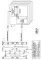
- To read out in unrotated form, the data is read out as it was stored and then shifted backto reproduce the original image. This prior art system for loading or reading is shown in Figs 3 and4. The 8K by 8K buffer is segmented into 16 bit words and there are a total of 4,194,304 words,which requires a 22 bit word counter. The least significant 9 lines, C0 through C8, count the words ineach vertical line of blocks in the image (512), bits C9 - C12 count the row lines within the block(16x16 bit block) and the remaining 9 address lines C13 - C21, count the blocks in the horizontaldirection of the image . Counter bits, C9-C12, are identical in value to the number of bits that thedata must be shifted before loading, and therefore are used to control the shifter as well as addressthe buffer.
- During read-out of an unrotated image these counter bits are used as shown in Fig 3. C0 -C8 are connected to A0 - A8 of the memory devices and used to address the blocks in the verticaldirection, C13 - C21 are connected to A13 - A21 of the memory devices and used to address theblocks in the horizontal direction, and C9 - C12 are connected to A9 - A12 and used to address thelines within the 16-blocks and also to control the shifter to shift the data back to its original position.
- Fig 4 shows the location of data in page buffer. As shown, the image is divided up into 16line (in the horizontal direction) by sixteen bit (per word) blocks. For the first block, address lines A0- A8 and A13 - A21 are all 0. For the second block in the scan line direction, the address lines A0 -
A8 equal 1 and the address lines A13 -A21 equal 0. Within the block, individual words areaddressed by address lines A9 - A12. - During loading or reading of a non-rotated image in the prior art, each entire scan line of512 words is completely read in or out before the next line is started. For a rotated image, the read-inis identical, but on read-out, the process reads out the same diagonal line from every block in thehorizontal line of blocks before going on to the next diagonal line in all of the blocks in the samehorizontal line, until all the diagonal lines in the 16-bit block are accessed. Then, the process readsout the diagonal lines from every block in the next set of 16-bit blocks in the horizontal direction.Therefore, for each random access memory (RAM), each consecutive read comes from a differentrow, and the slow page mode must be used. This entire prior art addressing system is shown in Fig5. The addressing lines A13 - A21 of the memory devices for addressing the 16-bit blocks in thehorizontal direction are taken from the counter C0 - C8, and lines A0 - A8 of the memory devices toaddress the 16-bit blocks in the vertical direction are taken from the counter C13 - C21. Then, foreach bit within the block, the address lines A9 - A12 to each RAM device are a function of counterbits C9 - C12. Here the process is to read out the same diagonal line, as defined by bits 9 - 12, ineach of the 512 blocks in the horizontal direction before going on to the next diagonal line.
- Fig 6 is a circuit of the prior art addressing arrangement shown in Figs 3 and 5. At thispoint is should be noted that while the image is 512 words by 8K bits, the memory is configured as2K by 2K, which requires 11 address lines for row and column addresses. Therefore, for non-rotatedimages, bits C0 - C10 are used for column addressing and C11 - 21 are used for the rows.
- For rotated images, the
multiplexers - Fig 7 is the schematic diagram of the present invention. Here, the arrangement of the
counter 10 andmultiplexers - In terms of performance, if data can be accessed at the rate of 200 megabits/second(Mbits/sec) for an unrotated image using the fast page mode and 80 Mbits/sec for a rotated imagenot using the fast page mode, then, with this invention, data can be accessed at 191.3 Mbits/sec foran unrotated image, and at 183.8 Mbits/sec for a rotated image. Thus, with this invention, speedsapproaching the fast page mode are available under all circumstances.
Claims (1)
- A circuit for addressing one bit at a time in a random access memory device (14)having x address lines divided into column address lines and row address lines, thecircuit comprising:characterised in that the y least significant bit (AO - A8) output lines of theregister (11) are divided into lower least significant bit (A0 - A5) output lines andupper least significant bit (A6 - A8) output lines,an x bit counter (10) having y least significant bits, z most significant bits, and nintermediate bits, where y + z + n = x, and x, y, z and n are positive integers,a first multiplexer (12) connected to the counter (10) and having A and B inputsand an output, the A and B inputs being connected to the counter (10) with the A inputbeing coupled to the y least significant bits and the B input being coupled to the zmost significant bits;a second multiplexer (13) connected to the counter (10) and having A' and B'inputs and an output, the A' and B' inputs being connected to the counter (10) withthe A' input being coupled to the z most significant bits and the B' input being coupledto the y least significant bits;a register (11) having y + z + n input and output lines wherein the y leastsignificant of the input lines (AO - A8) thereof are coupled to the output of the firstmultiplexer (12), the n intermediate input lines (A9 - A12) thereof are coupled to the nintermediate bits (C9 - C12) of the counter (10) and the z most significant of the inputlines (A13 - A21) thereof are coupled to the output of the second multiplexer (13),wherein the multiplexers (12, 13) in a first state couple the A and A' inputs to theregister (11) and in a second state couple the B and B', inputs to the register (11);the z most significant bit (A13 - A21) output lines of the register (11) are dividedinto lower most significant bit (A13 - A17) output lines and upper most significant bit(A18 - A21) output lines,said lower least significant bit (A0 - A5) output lines and said lower mostsignificant bit (A13 - A17) output lines being coupled to the column address lines ofthe random access memory device (14),said upper least significant bit (A6 - A8) output lines, the intermediate bit (A9 -A12) output lines and said upper most significant bit (A18 - A21) output lines of theregister (11) being coupled to the row address lines of the random access memorydevice (14).
Applications Claiming Priority (2)
| Application Number | Priority Date | Filing Date | Title |
|---|---|---|---|
| US878192 | 1992-05-04 | ||
| US07/878,192US5361339A (en) | 1992-05-04 | 1992-05-04 | Circuit for fast page mode addressing of a RAM with multiplexed row and column address lines |
Publications (3)
| Publication Number | Publication Date |
|---|---|
| EP0569218A2 EP0569218A2 (en) | 1993-11-10 |
| EP0569218A3 EP0569218A3 (en) | 1994-07-27 |
| EP0569218B1true EP0569218B1 (en) | 2001-10-31 |
Family
ID=25371561
Family Applications (1)
| Application Number | Title | Priority Date | Filing Date |
|---|---|---|---|
| EP93303466AExpired - LifetimeEP0569218B1 (en) | 1992-05-04 | 1993-05-04 | Circuit for rotating a ditigal image |
Country Status (4)
| Country | Link |
|---|---|
| US (1) | US5361339A (en) |
| EP (1) | EP0569218B1 (en) |
| JP (1) | JP3222979B2 (en) |
| DE (1) | DE69331027T2 (en) |
Families Citing this family (13)
| Publication number | Priority date | Publication date | Assignee | Title |
|---|---|---|---|---|
| US5561777A (en)* | 1993-08-30 | 1996-10-01 | Xerox Corporation | Process for sequentially reading a page from an image memory in either of two directions |
| US5663749A (en)* | 1995-03-21 | 1997-09-02 | Texas Instruments Incorporated | Single-buffer data formatter for spatial light modulator |
| KR970703568A (en)* | 1995-04-07 | 1997-07-03 | 이시마루 미키오 | METHOD AND APPARATUS FOR IMAGE POTATION |
| US5668980A (en)* | 1995-07-31 | 1997-09-16 | Advanced Micro Devices, Inc. | System for performing rotation of pixel matrices |
| US5761694A (en)* | 1995-11-30 | 1998-06-02 | Cirrus Logic, Inc. | Multi-bank memory system and method having addresses switched between the row and column decoders in different banks |
| US5689472A (en)* | 1996-10-31 | 1997-11-18 | Silicon Magic Corporation | System and method for providing efficient access to a memory bank |
| WO2001006371A1 (en)* | 1998-07-21 | 2001-01-25 | Seagate Technology Llc | Improved memory system apparatus and method |
| TW594743B (en)* | 2001-11-07 | 2004-06-21 | Fujitsu Ltd | Memory device and internal control method therefor |
| US7167148B2 (en)* | 2003-08-25 | 2007-01-23 | Texas Instruments Incorporated | Data processing methods and apparatus in digital display systems |
| US7315294B2 (en)* | 2003-08-25 | 2008-01-01 | Texas Instruments Incorporated | Deinterleaving transpose circuits in digital display systems |
| US7307635B1 (en)* | 2005-02-02 | 2007-12-11 | Neomagic Corp. | Display rotation using a small line buffer and optimized memory access |
| KR101525874B1 (en) | 2008-11-05 | 2015-06-04 | 삼성전자주식회사 | Buffer memory for rotating image, image pickup device and display device having the same |
| US10497438B2 (en) | 2017-04-14 | 2019-12-03 | Sandisk Technologies Llc | Cross-point memory array addressing |
Family Cites Families (9)
| Publication number | Priority date | Publication date | Assignee | Title |
|---|---|---|---|---|
| JPS5776649A (en)* | 1980-10-31 | 1982-05-13 | Toshiba Corp | Picture information display device |
| US4460958A (en)* | 1981-01-26 | 1984-07-17 | Rca Corporation | Window-scanned memory |
| US4500958A (en)* | 1982-04-21 | 1985-02-19 | Digital Equipment Corporation | Memory controller with data rotation arrangement |
| DE3713627A1 (en)* | 1986-04-23 | 1987-10-29 | Casio Computer Co Ltd | IMAGE STORAGE CIRCUIT, IN PARTICULAR FOR USE IN ROTATING IMAGE DATA |
| JPS63177235A (en)* | 1987-01-19 | 1988-07-21 | Fujitsu Ltd | multidimensional access memory |
| US4965751A (en)* | 1987-08-18 | 1990-10-23 | Hewlett-Packard Company | Graphics system with programmable tile size and multiplexed pixel data and partial pixel addresses based on tile size |
| US5012434A (en)* | 1989-02-21 | 1991-04-30 | Siemens Aktiengesellschaft | Apparatus and method for selective rotation of data printed by a matrix printer |
| ATE103752T1 (en)* | 1989-07-14 | 1994-04-15 | Siemens Ag | METHOD FOR STORING VIDEO SIGNAL DATA AND DEVICE FOR CARRYING OUT THE METHOD. |
| US5111192A (en)* | 1989-12-20 | 1992-05-05 | Xerox Corporation | Method to rotate a bitmap image 90 degrees |
- 1992
- 1992-05-04USUS07/878,192patent/US5361339A/ennot_activeExpired - Fee Related
- 1993
- 1993-04-27JPJP10151193Apatent/JP3222979B2/ennot_activeExpired - Fee Related
- 1993-05-04DEDE69331027Tpatent/DE69331027T2/ennot_activeExpired - Fee Related
- 1993-05-04EPEP93303466Apatent/EP0569218B1/ennot_activeExpired - Lifetime
Also Published As
| Publication number | Publication date |
|---|---|
| JPH0696196A (en) | 1994-04-08 |
| US5361339A (en) | 1994-11-01 |
| EP0569218A3 (en) | 1994-07-27 |
| EP0569218A2 (en) | 1993-11-10 |
| JP3222979B2 (en) | 2001-10-29 |
| DE69331027D1 (en) | 2001-12-06 |
| DE69331027T2 (en) | 2002-03-21 |
Similar Documents
| Publication | Publication Date | Title |
|---|---|---|
| US5111192A (en) | Method to rotate a bitmap image 90 degrees | |
| US5561777A (en) | Process for sequentially reading a page from an image memory in either of two directions | |
| CA1122696A (en) | Image rotation apparatus | |
| EP0569218B1 (en) | Circuit for rotating a ditigal image | |
| EP0225059B1 (en) | Semiconductor memory | |
| US4052699A (en) | High speed real time image transformation | |
| EP0492939B1 (en) | Method and apparatus for arranging access of VRAM to provide accelerated writing of vertical lines to an output display | |
| US4806920A (en) | Device for producing an output image while giving an original image a rotation of 90, 180, or 270 | |
| US4561072A (en) | Memory system handling a plurality of bits as a unit to be processed | |
| EP0398510B1 (en) | Video random access memory | |
| EP0279228A2 (en) | A frame buffer in or for a raster scan video display | |
| US5408539A (en) | Tessellating and quadding pels during image transfer | |
| US5675826A (en) | Image data storage | |
| EP0200036B1 (en) | Method and system for displaying images in adjacent display areas | |
| US5450355A (en) | Multi-port memory device | |
| US6085304A (en) | Interface for processing element array | |
| JPH06101039B2 (en) | Window image data read processing method | |
| US5991186A (en) | Four-bit block write for a wide input/output random access memory in a data processing system | |
| KR100297716B1 (en) | Semiconductor memory device having high flexibility in column | |
| EP0130340B1 (en) | Memory mapping and readout system | |
| US5005073A (en) | Demultiplexer for providing a color television signal having an increased image frequency | |
| US4888584A (en) | Vector pattern processing circuit for bit map display system | |
| KR0138740B1 (en) | Signal Display Method of Ultrasonic Diagnostic Machine | |
| JPS60211690A (en) | Memory circuit | |
| JPH0410095B2 (en) |
Legal Events
| Date | Code | Title | Description |
|---|---|---|---|
| PUAI | Public reference made under article 153(3) epc to a published international application that has entered the european phase | Free format text:ORIGINAL CODE: 0009012 | |
| AK | Designated contracting states | Kind code of ref document:A2 Designated state(s):DE FR GB | |
| PUAL | Search report despatched | Free format text:ORIGINAL CODE: 0009013 | |
| AK | Designated contracting states | Kind code of ref document:A3 Designated state(s):DE FR GB | |
| RHK1 | Main classification (correction) | Ipc:G11C 8/00 | |
| 17P | Request for examination filed | Effective date:19950127 | |
| 17Q | First examination report despatched | Effective date:19970613 | |
| APAB | Appeal dossier modified | Free format text:ORIGINAL CODE: EPIDOS NOAPE | |
| APAD | Appeal reference recorded | Free format text:ORIGINAL CODE: EPIDOS REFNE | |
| APCB | Communication from the board of appeal sent | Free format text:ORIGINAL CODE: EPIDOS OBAPE | |
| APCB | Communication from the board of appeal sent | Free format text:ORIGINAL CODE: EPIDOS OBAPE | |
| APAB | Appeal dossier modified | Free format text:ORIGINAL CODE: EPIDOS NOAPE | |
| GRAG | Despatch of communication of intention to grant | Free format text:ORIGINAL CODE: EPIDOS AGRA | |
| GRAG | Despatch of communication of intention to grant | Free format text:ORIGINAL CODE: EPIDOS AGRA | |
| GRAH | Despatch of communication of intention to grant a patent | Free format text:ORIGINAL CODE: EPIDOS IGRA | |
| GRAH | Despatch of communication of intention to grant a patent | Free format text:ORIGINAL CODE: EPIDOS IGRA | |
| GRAA | (expected) grant | Free format text:ORIGINAL CODE: 0009210 | |
| AK | Designated contracting states | Kind code of ref document:B1 Designated state(s):DE FR GB | |
| REF | Corresponds to: | Ref document number:69331027 Country of ref document:DE Date of ref document:20011206 | |
| REG | Reference to a national code | Ref country code:GB Ref legal event code:IF02 | |
| PLBE | No opposition filed within time limit | Free format text:ORIGINAL CODE: 0009261 | |
| STAA | Information on the status of an ep patent application or granted ep patent | Free format text:STATUS: NO OPPOSITION FILED WITHIN TIME LIMIT | |
| 26N | No opposition filed | ||
| REG | Reference to a national code | Ref country code:GB Ref legal event code:746 Effective date:20050404 | |
| PGFP | Annual fee paid to national office [announced via postgrant information from national office to epo] | Ref country code:DE Payment date:20050428 Year of fee payment:13 | |
| PGFP | Annual fee paid to national office [announced via postgrant information from national office to epo] | Ref country code:GB Payment date:20050504 Year of fee payment:13 | |
| PGFP | Annual fee paid to national office [announced via postgrant information from national office to epo] | Ref country code:FR Payment date:20050511 Year of fee payment:13 | |
| APAH | Appeal reference modified | Free format text:ORIGINAL CODE: EPIDOSCREFNO | |
| PG25 | Lapsed in a contracting state [announced via postgrant information from national office to epo] | Ref country code:GB Free format text:LAPSE BECAUSE OF NON-PAYMENT OF DUE FEES Effective date:20060504 | |
| PG25 | Lapsed in a contracting state [announced via postgrant information from national office to epo] | Ref country code:DE Free format text:LAPSE BECAUSE OF NON-PAYMENT OF DUE FEES Effective date:20061201 | |
| GBPC | Gb: european patent ceased through non-payment of renewal fee | Effective date:20060504 | |
| REG | Reference to a national code | Ref country code:FR Ref legal event code:ST Effective date:20070131 | |
| PG25 | Lapsed in a contracting state [announced via postgrant information from national office to epo] | Ref country code:FR Free format text:LAPSE BECAUSE OF NON-PAYMENT OF DUE FEES Effective date:20060531 |