EP0569137B1 - Programmable logic array integrated circuit - Google Patents
Programmable logic array integrated circuitDownload PDFInfo
- Publication number
- EP0569137B1 EP0569137B1EP93302745AEP93302745AEP0569137B1EP 0569137 B1EP0569137 B1EP 0569137B1EP 93302745 AEP93302745 AEP 93302745AEP 93302745 AEP93302745 AEP 93302745AEP 0569137 B1EP0569137 B1EP 0569137B1
- Authority
- EP
- European Patent Office
- Prior art keywords
- conductors
- logic
- programmable logic
- programmable
- blocks
- Prior art date
- Legal status (The legal status is an assumption and is not a legal conclusion. Google has not performed a legal analysis and makes no representation as to the accuracy of the status listed.)
- Expired - Lifetime
Links
- 239000004020conductorSubstances0.000claimsdescription149
- 102100040862Dual specificity protein kinase CLK1Human genes0.000claims1
- 102100040844Dual specificity protein kinase CLK2Human genes0.000claims1
- 101000749294Homo sapiens Dual specificity protein kinase CLK1Proteins0.000claims1
- 101000749291Homo sapiens Dual specificity protein kinase CLK2Proteins0.000claims1
- 230000006870functionEffects0.000description14
- 230000000295complement effectEffects0.000description9
- 238000010586diagramMethods0.000description8
- 230000008901benefitEffects0.000description3
- 238000010276constructionMethods0.000description2
- 239000012634fragmentSubstances0.000description2
- 230000015654memoryEffects0.000description2
- 239000002184metalSubstances0.000description2
- 238000000034methodMethods0.000description2
- 238000012986modificationMethods0.000description2
- 230000004048modificationEffects0.000description2
- 230000005540biological transmissionEffects0.000description1
- 239000000872bufferSubstances0.000description1
- 230000006872improvementEffects0.000description1
- 230000008520organizationEffects0.000description1
- 230000037361pathwayEffects0.000description1
- 230000001360synchronised effectEffects0.000description1
Images


Classifications
- H—ELECTRICITY
- H03—ELECTRONIC CIRCUITRY
- H03K—PULSE TECHNIQUE
- H03K19/00—Logic circuits, i.e. having at least two inputs acting on one output; Inverting circuits
- H03K19/02—Logic circuits, i.e. having at least two inputs acting on one output; Inverting circuits using specified components
- H03K19/173—Logic circuits, i.e. having at least two inputs acting on one output; Inverting circuits using specified components using elementary logic circuits as components
- H03K19/177—Logic circuits, i.e. having at least two inputs acting on one output; Inverting circuits using specified components using elementary logic circuits as components arranged in matrix form
- H03K19/17736—Structural details of routing resources
- H—ELECTRICITY
- H03—ELECTRONIC CIRCUITRY
- H03K—PULSE TECHNIQUE
- H03K19/00—Logic circuits, i.e. having at least two inputs acting on one output; Inverting circuits
- H03K19/02—Logic circuits, i.e. having at least two inputs acting on one output; Inverting circuits using specified components
- H03K19/173—Logic circuits, i.e. having at least two inputs acting on one output; Inverting circuits using specified components using elementary logic circuits as components
- H03K19/177—Logic circuits, i.e. having at least two inputs acting on one output; Inverting circuits using specified components using elementary logic circuits as components arranged in matrix form
- H03K19/17704—Logic circuits, i.e. having at least two inputs acting on one output; Inverting circuits using specified components using elementary logic circuits as components arranged in matrix form the logic functions being realised by the interconnection of rows and columns
- H—ELECTRICITY
- H03—ELECTRONIC CIRCUITRY
- H03K—PULSE TECHNIQUE
- H03K19/00—Logic circuits, i.e. having at least two inputs acting on one output; Inverting circuits
- H03K19/02—Logic circuits, i.e. having at least two inputs acting on one output; Inverting circuits using specified components
- H03K19/173—Logic circuits, i.e. having at least two inputs acting on one output; Inverting circuits using specified components using elementary logic circuits as components
- H03K19/177—Logic circuits, i.e. having at least two inputs acting on one output; Inverting circuits using specified components using elementary logic circuits as components arranged in matrix form
- H03K19/17724—Structural details of logic blocks
- H03K19/17728—Reconfigurable logic blocks, e.g. lookup tables
- H—ELECTRICITY
- H03—ELECTRONIC CIRCUITRY
- H03K—PULSE TECHNIQUE
- H03K19/00—Logic circuits, i.e. having at least two inputs acting on one output; Inverting circuits
- H03K19/02—Logic circuits, i.e. having at least two inputs acting on one output; Inverting circuits using specified components
- H03K19/173—Logic circuits, i.e. having at least two inputs acting on one output; Inverting circuits using specified components using elementary logic circuits as components
- H03K19/177—Logic circuits, i.e. having at least two inputs acting on one output; Inverting circuits using specified components using elementary logic circuits as components arranged in matrix form
- H03K19/17736—Structural details of routing resources
- H03K19/1774—Structural details of routing resources for global signals, e.g. clock, reset
- H—ELECTRICITY
- H03—ELECTRONIC CIRCUITRY
- H03K—PULSE TECHNIQUE
- H03K19/00—Logic circuits, i.e. having at least two inputs acting on one output; Inverting circuits
- H03K19/02—Logic circuits, i.e. having at least two inputs acting on one output; Inverting circuits using specified components
- H03K19/173—Logic circuits, i.e. having at least two inputs acting on one output; Inverting circuits using specified components using elementary logic circuits as components
- H03K19/177—Logic circuits, i.e. having at least two inputs acting on one output; Inverting circuits using specified components using elementary logic circuits as components arranged in matrix form
- H03K19/1778—Structural details for adapting physical parameters
- H03K19/17792—Structural details for adapting physical parameters for operating speed
Definitions
- This inventionrelates to programmable logic array integrated circuits, and more particularly to a programmable logic array integrated circuit having improved and more diverse interconnections between the individual logic modules.
- EP-A-0530985which falls within the terms of Article 54(3) EPC, shows programmable logic array integrated circuits which are highly modular. In the circuits shown in that application, very similar types of interconnection pathways are used for all types of interconnections between the logic modules. This tends to simplify the design of the circuit. It also tends to simplify the software and/or other techniques used to program the circuit to implement particular logic functions. Thus the circuits shown in the above-mentioned application have several important advantages.
- a programmable logic array integrated circuitincluding a plurality of logic modules, each of which has a plurality of inputs and an output for producing at said output a programmable logical function of said inputs, said logic modules being grouped in a plurality of logic array blocks, said blocks being disposed in a two dimensional array including intersecting rows and columns of said blocks; a plurality of first conductors associated with each of said blocks for selectively applying the outputs of the logic modules in the associated block to the inputs of the logic modules in that block; a plurality of second conductors extending substantially parallel to a first dimension of said array, said second conductors being grouped in a plurality of groups, each of which groups is associated with a respective one of said rows of blocks, each second conductor in each of said groups of second conductors extending continuously past substantially all of the blocks in the associated row; a plurality of third conductors extending substantially parallel to a second dimension of said array, said third conductors being grouped in a said array
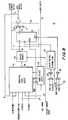
- FIG. 1is a simplified schematic block diagram of an illustrative programmable logic array integrated circuit constructed in accordance with the principles of the invention.
- FIG. 2is a more detailed schematic block diagram of an illustrative embodiment of a representative portion of the circuit shown in FIG. 1.
- FIG. 3is a still more detailed schematic block diagram of an illustrative embodiment of a representative portion of the circuitry shown in FIG. 2.
- FIG. 4is a schematic block diagram of an illustrative embodiment of a portion of the circuitry shown in FIG. 3.
- FIG. 5is another view of the circuit of FIG. 1 showing an illustrative embodiment of additional elements of that circuit.
- FIGS. 6a and 6bare schematic block diagrams showing an illustrative embodiment of representative portions of FIG. 5 in more detail.
- FIGS. 7a through 7care schematic diagrams showing illustrative alternative embodiments of portions of the circuitry shown in FIG. 3.
- FIG. 8is another more detailed schematic block diagram of an illustrative embodiment of a representative portion of FIG. 2.
- FIG. 9is a schematic diagram of an illustrative embodiment of a representative element shown in FIG. 2.
- FIG. 1shows the overall organization of an illustrative programmable logic array integrated circuit 10 constructed in accordance with the principles of this invention. Not all of the conductors employed in circuit 10 are shown in FIG. 1, but enough is shown in this FIG. to begin the discussion.
- Each logic module 12is represented by a small square in FIG. 1.
- Logic modules 12are grouped together in groups of eight. Each of these groups is referred to as a logic array block or LAB 14.
- LABs 14are arranged in six horizontal rows and 22 vertical columns on circuit 10. Accordingly, there are a total of 132 LABs 14 and 1056 logic modules 12 on circuit 10.
- Each logic module 12is capable of performing a relatively elementary logic function (discussed in more detail below), but extremely complex logic can be performed by variously interconnecting the logic modules as will now be discussed.
- the interconnection circuitry shown in FIG. 1includes (1) groups of so-called global horizontal conductors 20 interspersed between the horizontal rows of LABs, and (2) groups of global vertical conductors 22 interspersed between the vertical columns of LABs. These conductors are global in the sense that they extend along an entire row or column. Programmable interconnections can be made between intersecting horizontal and vertical conductors in order to apply signals on the vertical conductors to the horizontal conductors.
- Each LAB 14has a group of vertical LAB input conductors 24 for conveying signals from the global horizontal conductors 20 intersected by conductors 24 to the logic modules 12 in that LAB.
- FIG. 1shows part of a network of so-called universal fast conductors.
- the conductors 30 of this network shown in FIG. 1extend throughout the entire circuit and can be used as will be described in more detail below to convey widely used logic signals such as clock and/or clear signals to any logic modules 12 on the circuit.
- each logic module 12includes a look up table or universal logic block (“ULB") 40 and a flip-flop type device 142.
- Each look up table 40is basically a circuit which can be programmed to produce an output signal which is any logical function of four input signals applied to the look up table.
- Each flip-flop 142is a circuit which can be programmed either to store or to simply pass through the output signal of the associated look up table (see, for example, the circuit shown in Norman et al. U.S. patent 4,864,161, corresponding to EP-A-0 350 141).
- device 142could be a flip-flop with no pass through or bypass capability.
- FIG. 2shows portions of representative global horizontal conductors 20, global vertical conductors 22, LAB input conductors 24, and universal fast conductors 30.
- Each of LAB input conductors 24can be connected to a selected one (or more) of conductors 20 and 30 via a programmably controlled programmable logic connector (“PLC") 50 (only some of which are shown in FIG. 2).
- PLCs 50can be implemented in any of a wide variety of ways.
- each PLC 50can be a relatively simple programmable connector such as a plurality of switches for connecting any one of several inputs to an output.
- each PLCcan be a somewhat more complex element which is capable of performing logic (e.g., by logically combining several of its inputs) as well as making a connection.
- each PLCcan be product term logic implementing functions such as AND, NAND, OR, or NOR.
- Examples of components suitable for implementing PLCs 50are EPROMs, EEPROMs, pass transistors, transmission gates, antifuses, laser fuses, metal optional links, etc.
- FCEsfunction control elements
- each PLC 50is a 15-to-1 switch which is controlled by programmable function control elements ("FCEs") 51 on circuit 10 to connect one of its 15 inputs to its output.
- FCEsprogrammable function control elements
- Each of the 15 inputsis the signal on a predetermined respective one of conductors 20 or 30.
- Each of conductors 20 and 30is connected to two of PLCs 50. Accordingly, each of conductors 20 and 30 is connectable to two of conductors 24.
- the letter P and the associated arrow symbol inside dotted line 49indicate that the population of connections from conductors 20 and 30 to the inputs of each of PLCs 50 is a partial population.
- FCEs 51can also be implemented in any of several different ways.
- FCEs 51can be SRAMs, DRAMs, first-in first-out ("FIFO") memories, EPROMs, EEPROMs, function control registers (e.g., as in Wahlstrom U.S. patent 3,473,160), ferro-electric memories, fuses, antifuses, or the like.
- Each of the four data inputs to each logic module 12can be connected to any one (or more) of LAB input conductors 24 (and/or any one (or more) of local conductors 26) via a PLC 52.
- PLCs 52(and each similar PLC 34 which are discussed below) may have any of the characteristics described above for the general case of PLCs 50.
- each of PLCs 52(and each similar PLC 34) is a 32-to-1 switch so that any one of the 24 LAB input conductors 24 or any one of the eight local conductors 26 can be connected to each LAB data input.
- the letter F and the associated arrow symbol inside chain dotted line 53indicate that the population of connections from conductors 24 and 26 to PLCs 34 and 52 is a full population.
- the FCEs(similar to above-described FCEs 51) for programmably controlling PLCs 34 and 52 are not shown separately, but rather are assumed to be part of elements 34 and 52.
- the data output of the flip-flop 142 in each logic module 12can be applied (via conductor 54) to a respective one of local conductors 26. These conductors serve only the logic modules in the associated LAB 14. In other words, conductors 26 do not extend beyond the associated LAB.
- the data output of the flip-flop 142 in each logic module 12can also be applied to either or both of two global vertical conductors 22 (via tri-state drivers 56), and to one of global horizontal conductors 20 (via PLC 58 and tri-state driver 60).
- the other input or inputs to each PLC 58are the signals from one or more of global vertical conductors 22. Accordingly, global vertical conductors 22 are selectively connectable to global horizontal conductors 20 via PLCs 58 and tri-state drivers 60.
- PLCs 58may be similar to any of the above-described PLCs.
- the use of tri-state drivers 56 and 60is advantageous to strengthen signals which may be required to travel relatively long distances throughout circuit 10 and/or which may be inputs to relatively large numbers of other components.
- a suitable tri-state driveris shown in FIG. 9 and described in detail below.
- Some or all of tri-state drivers 56 and 60may be controlled (i.e., turned on or off) by FCEs (e.g., FCEs 57) on circuit 10.
- FCEse.g., FCEs 57
- PLCs 58are also typically controlled by FCES on the circuit. All of these FCEs may be similar to above-described FCEs 51.
- each of PLCs 34is a 32-to-1 switch, but PLCs 34 can alternatively have any of the characteristics described above for the general case of PLCs 50. Although only two PLCs 34 are shown in FIG. 2, there is preferably one such PLC for each of the four conductors 32.
- Each of conductors 32is connectable to any one of universal fast conductors 30 for receiving the signal on the fast conductor.
- connections from conductors 30 to conductors 32are preferably made in the same way that the connections from conductors 24 and 26 to conductors 32 are made, i.e., by PLCs controlled by FCEs (all represented by element 31 in FIG. 2).
- PLCs controlled by FCEsall represented by element 31 in FIG. 2.
- FCEsall represented by element 31 in FIG. 2.
- each of these PLCscan have any of the characteristics described above for the general case of PLCs 50, in the depicted, presently preferred embodiment each of these PLCs can connect any of conductors 30 to an associated one of conductors 32.
- the letter F and the arrow symbol inside chain dotted line 31indicate that the population of possible connections from conductors 30 to each of conductors 32 is a full population.
- Each of conductors 32is connectable (via conductors 36) to each of logic modules 12.
- FCE-controlled PLCs in each logic moduleallow these signals to be used for such purposes as flip-flop clock and flip-flop clear (see FIG. 8 (discussed below) which shows an illustrative logic module 12 in more detail).
- local vertical conductors 32are known as clock and clear lines and can be driven from fast lines 30 for synchronous clocks and clears (i.e., clocks and clears which come from outside of device 10 and are available everywhere throughout device 10), or from LAB input lines 24 or local lines 26.
- carry chain interconnections 70a and 70bThere are two other types of logic module interconnections shown in FIG. 2 which require discussion.
- the first of theseis carry chain interconnection represented in part by conductors 70a and 70b.
- These interconnectionsallow a carry out output of each logic module 12 to be used as a carry in input to an adjacent or nearby logic module as shown, for example, in U.S. patent No. 5,274,581, corresponding to EP-A-0 569 135 (see also FIG. 8 herein).
- carry chain conductors 70aallow the carry out output of each logic module 12 shown in FIG. 2 to be the carry in input to the next higher logic module in that FIG.
- carry chain conductor 70bruns from the topmost logic module 12 in the LAB fragment shown in FIG. 2 to the bottom-most logic module in the horizontally adjacent LAB in the adjacent column of LABs. This allows the carry chain to continue from LAB to LAB if desired.
- a typical logic module 12includes look up table or ULE 40 which is controlled by 16 FCEs 44 to produce on data output lead 46 any desired logical function of the four data input signals from PLCs 52.
- a representative FCE 44is depicted as a RAM cell, it will be understood that FCEs 44 can be implemented in any of a wide variety of ways as discussed above in connection with FCEs 51).
- the signal on lead 46is applied to one input of AND gate 48. (Although shown as an AND gate in FIG.
- cascade connect device 48could alternatively be any other suitable two-input logic function such as an EXCLUSIVE OR gate.
- the other input to AND gate 48is the cascade connect input from another logic module 12 gated by transistor 74a which is controlled by FCE 74b (similar to previously described FCEs).
- transistor 74ais disabled by FCE 74b, then transistor 74c is enabled to connect the second input of AND gate 48 to a source of logical 1 potential.
- AND gate 48produces an output signal on lead 76 which is the logical AND of the signals on incoming leads 46 and 72.
- the signal on lead 76can therefore be a significantly more complex logic function than could be produced by one look up table 40 by itself.
- the signal on lead 76is also applied to another cascade connect conductor 72 for cascade connection to another adjacent or nearby logic module 12 in the same way that the incoming lead 72 shown in FIG. 3 is connected to the logic module shown in that FIG.
- FIG. 2shows that each cascade connect conductor 72a from a logic module 12 is connected to the next higher logic module in that FIG.
- the cascade connect output from the top-most logic module 12 in FIG. 2goes (via cascade connect conductor 72b) to logic modules in an adjacent column of LABs (e.g., to the bottom-most logic modules in the LAB immediately to the right of the LAB fragment shown in FIG. 2).
- FIG. 4shows a typical basic look up table 40 in more detail.
- Look up table 40may be modified as shown in above-mentioned patent No. 5,274,581 (corresponding to EP-A-0 569 135) to facilitate performance of fast carry logic, but FIG. 4 shows the basic structure of a four-input look up table.)
- This tableis controlled by 16 FCEs 44.
- the output signal of each of these FCEsis applied to a respective one of 16 AND gates 80.
- Alternate ones of AND gates 80are respectively controlled by the true and complement of the first data input J, the complement of input J being produced by inverter I1.
- the outputs of adjacent pairs of switches 80are then combined by OR gates 81 and applied to eight AND gates 82.
- Alternate ones of AND gates 82are respectively controlled by the true and complement of the second data input K, the complement of input K being produced by inverter I2.
- the outputs of adjacent pairs of AND gates 82are combined by OR gates 83 and then applied to four AND gates 84.
- Alternate ones of AND gates 84are respectively controlled by the true and complement of the third data input L, the complement of input L being produced by inverter I3.
- the outputs of adjacent pairs of AND gates 84are combined by OR gates 85 and applied to two AND gates 86.
- One of AND gates 86is controlled by the true of the fourth data input M, while the other AND gate 86 is controlled by the complement of that input (produced by inverter I4).
- the outputs of AND gates 86are combined by OR gate 87 to produce the data output on conductor 46. It will be apparent from the foregoing that any desired logical function of data inputs J-M can be produced by appropriately programming FCEs 44.
- FIG. 5shows how input/output pins may be provided on circuit 10.
- Six groups 90 of eight input/output pinsare shown along each side of circuit 10.
- Twenty-two groups 92 of two input/output pinsare shown along each of the top and bottom of the circuit.
- FIGS. 6a and 6bshow parts of an illustrative embodiment of such an arrangement.
- the 176 global horizontal conductors 20 associated with each horizontal row of LABs 14are arranged so that half can receive the outputs of the drivers 60 (FIG. 2) associated with the top four logic modules 12 in each LAB in that row, while the other half of these conductors 20 can receive the outputs of the drivers 60 associated with the lower four logic modules 12 in each LAB in that row. Accordingly, in FIG.
- each group of 176 global horizontal conductors 20is shown divided into two subgroups of 88 such conductors, one subgroup being above the associated row of LABs 14, and the other subgroup being below that row of LABs.
- Each input/output pin 100 in each group 90 of such pinscan receive an output via a PLC 102 from the conductors 20 in two subgroups of 88 such conductors.
- PLCs 102can have any of the characteristics described above for the general case of PLCs 50, and PLCs 102 are controlled by programmable FCEs similar to those described above.)
- One of these two subgroups of conductorsis associated with the lower logic modules 12 in one row of LABs 14, while the other subgroup of conductors is associated with the upper logic modules 12 in the LAB row immediately below the first row.
- each pin 100is connected through two tri-state drivers to two of conductors 20.
- each symbol 104 in FIG. 6arepresents two tri-state drivers, each of which is programmably controlled (e.g., by an FCE similar to those described above).
- each vertical row of LABs 14are split into two groups of eight conductors at the top and bottom of the device.
- Each group of eight conductorsis applied to a respective one of PLCs 103 (similar to the above-described PLCs).
- PLCs 103applies one (or more) of the signals applied to it to an associated input/output pin 101.
- each pin 101is connected through two programmable tri-state drivers 105 to two of conductors 22.
- logic modules 12can be implemented in other ways.
- the portion of each logic module 12 which is described above as a look up table 40can alternatively be implemented as sum-of-products logic of the type shown in FIG. 7a.
- the particular logic shown in FIG. 7ais of the well known "programmable AND, fixed OR" type.
- the true or complement of any of inputs A-D(which correspond to signals A-D in FIG. 3) is programmably connectable to each of AND gates 202a-e. Accordingly, each of these AND gates produces the logical "product" of the inputs connected to it.
- These productsare sometimes referred to as "product terms" or "pterms”.
- the outputs of AND gates 202a-dare all applied to OR gate 204.
- the output signal of OR gate 204is therefore the logical "sum" of the applied pterms.
- the output of OR gate 204is applied to EXCLUSIVE OR gate 206.
- the other input to gate 206is pterm 202e. Accordingly, pterm 202e can be used (in conjunction with gate 206) to selectively invert or otherwise gate the sum-of-products output of OR gate 204.
- the output of gate 206is applied to EXCLUSIVE OR gate 208.
- the other input to gate 208is the output signal of programmable FCE 210 (similar to the other FCEs described above). Accordingly, FCE 210 can be used (in conjunction with gate 208) to selectively invert the output of gate 206.
- the output of gate 208can be applied, inter alia, to the data input of the register 42 of the logic module.
- FIGS. 7b and 7cStill other examples of possible logic module construction are shown in FIGS. 7b and 7c.
- each conductor 24 and 26(corresponding to conductors 24 and 26 in FIG. 2) is present in both the true and complement form. Pterms are formed in programmable connections between these conductors and the inputs to AND gates 202a-e. The remainder of each FIG. 7b logic module may then be similar to the corresponding portion of the circuitry shown in FIG. 7a.
- circuitry outside the rectangular boxesmay be identical to the corresponding portion of FIG. 7b.
- the circuitry represented by each rectangular box in FIG. 7cmay be the macrocell structure 100 shown in above-mentioned patent No. 5,121,006, corresponding to EP-A-0 510 830.
- FIG. 8is another depiction of an illustrative logic module 12 in accordance with this invention. Certain features shown in FIG. 8 -- especially those related to the implementation of fast carry logic and the use of logic modules of this type in adders and counters -- are shown in even more detail in above-mentioned patent No. 5,274,581. For example, that patent explains that input C is applied to flip-flop 42 as data (in addition to being applied to universal logic block 40) to facilitate loading data into the flip-flop when logic module 12 is to be used as one stage of a loadable counter.
- Cascade connect input 72is applied as one input to logic element 48 (typically an AND gate as described above in connection with FIG. 3).
- the desired signals on clock and clear lines 32are selected by programmable (i.e., FCE-controlled) PLCs 120 and 122.
- the output of PLC 122is applied to the clear input terminal of flip-flop 42.
- the output of PLC 120 and one of signals 32are applied to clock control and asynchronous load control logic 124 to produce a signal applied to the clock input terminal of flip-flop 42. This signal controls the clocking of flip-flop 42, as well as the asynchronous loading of that flip-flop (e.g., when loading the starting value into a loadable counter).
- the main data output 46 of universal logic block 40is the other input to logic element 48.
- the output of element 48is the D input to flip-flop 42 (for registered output from logic module 12).
- the output of element 48can also bypass flip-flop 42 via programmable (i.e., FCE-controlled) switch 130 (for unregistered output from the logic module).
- FCE 131controls switch 130.
- the output of element 48is also the cascade connect output 72 from this logic module to the next logic module 12 in the cascade connect chain.
- Universal logic block 40 in FIG. 8is equipped as shown in above-mentioned patent No. 5,274,581 to provide as outputs X and Y the logical NOR and logical NAND of two inputs to block 40.
- carry select logic 126inverts X and Y, and then uses fast carry input 70 to select the appropriate one of the inverted signals as the fast carry output 70 to be applied to the next logic module 12 in the fast carry chain.
- FIG. 9shows a typical tri-state driver 150 such as can be used for drivers 56 and 60 in FIG. 2. (Of course, any other suitable tri-state driver can be used instead if desired.)
- Datais applied to input terminal TRIIN, and a driver-enabling signal is applied to terminal RSELTRI (e.g., from a programmable RAM cell). If driver 150 is enabled by the latter signal, the input data is passed to output terminal TRIOUT.
- Driver 150has three stages. The first stage includes P-channel transistors MP0 and MP1 and N-channel transistor MN0 connected in series between VCC (logical 1) and ground (logical 0). The TRIIN terminal is connected to the gates of MP0 and MN0. The inverted RSELTRI signal is applied to the gate of MP1.
- the second stageincludes P-channel transistor MP2 and N-channel transistors MN1 and MN2 connected in series between VCC and ground.
- the RSELTRI signalis applied to the gates of MP2 and MN1.
- the signal between MP0 and MP1is applied between MP2 and MN1, as well as to the gate of third stage P-channel transistor MP3.
- the signal between MP1 and MN0is applied between MN1 and MN2, as well as to the gate of third stage N-channel transistor MN3.
- MP3 and MN3are connected in series between VCC and ground. The node between MP3 and MN3 is TRIOUT.
- tri-state driversis preferred for elements such as 56 and 60 in FIG. 2, in some embodiments of the invention it may be possible to employ simple buffers instead.
Landscapes
- Physics & Mathematics (AREA)
- Mathematical Physics (AREA)
- Engineering & Computer Science (AREA)
- Computer Hardware Design (AREA)
- Computing Systems (AREA)
- General Engineering & Computer Science (AREA)
- Computer Networks & Wireless Communication (AREA)
- Logic Circuits (AREA)
- Design And Manufacture Of Integrated Circuits (AREA)
Description
- This invention relates to programmable logic array integrated circuits, and more particularly to a programmable logic array integrated circuit having improved and more diverse interconnections between the individual logic modules.
- European patent application EP-A-0530985, which falls within the terms of Article 54(3) EPC, shows programmable logic array integrated circuits which are highly modular. In the circuits shown in that application, very similar types of interconnection pathways are used for all types of interconnections between the logic modules. This tends to simplify the design of the circuit. It also tends to simplify the software and/or other techniques used to program the circuit to implement particular logic functions. Thus the circuits shown in the above-mentioned application have several important advantages.
- There is always room for further improvement, however, and there are some situations in which the provision of additional or alternative types of interconnections between the logic modules would have benefits sufficient to justify the additional circuit and programming complexity. Such additional interconnection paths may be desirable for making frequently needed kinds of interconnections, for speeding certain kinds of interconnections, for allowing short distance connections to be made without tying up more general purpose and therefore long distance interconnection resources, etc. There is also a continuing demand for logic devices with larger capacity. This produces a need to implement logic functions more efficiently and to make better use of the portion of the device which is devoted to interconnecting individual logic modules.
- It is therefore an object of this invention to provide an improved programmable logic array integrated circuit.
- It is a more particular object of this invention to provide a programmable logic array integrated circuit with additional possibilities for interconnections between the logic modules.
- According to the invention there is provided a programmable logic array integrated circuit including a plurality of logic modules, each of which has a plurality of inputs and an output for producing at said output a programmable logical function of said inputs, said logic modules being grouped in a plurality of logic array blocks, said blocks being disposed in a two dimensional array including intersecting rows and columns of said blocks; a plurality of first conductors associated with each of said blocks for selectively applying the outputs of the logic modules in the associated block to the inputs of the logic modules in that block; a plurality of second conductors extending substantially parallel to a first dimension of said array, said second conductors being grouped in a plurality of groups, each of which groups is associated with a respective one of said rows of blocks, each second conductor in each of said groups of second conductors extending continuously past substantially all of the blocks in the associated row; a plurality of third conductors extending substantially parallel to a second dimension of said array, said third conductors being grouped in a said array, said third conductors being grouped in a plurality of groups, each of which groups is associated with a respective one of said columns of blocks, each third conductor in each of said groups of third conductors extending continuously past substantially all of the blocks in the associated column; means for selectively applying the output of each logic module to at least one of the second or third conductors in the group of second or third conductors associated with the block which includes that logic module; means for selectively connecting each of said second conductors to at least one of said third conductors; pluralities of fourth conductors, wherein each of said blocks is associated with a respective plurality of fourth conductors; means for selectively connecting to each of the fourth conductors associated with a respective block any one of a multiplicity of said second conductors in the group of second conductors associated with that block; and means for selectively connecting any one of said fourth conductors associated with a respective block to each of the inputs of the logic modules in that block.
- Further features of the invention, its nature and various advantages will be more apparent from the accompanying drawings and the following detailed description of the preferred embodiments.
- FIG. 1 is a simplified schematic block diagram of an illustrative programmable logic array integrated circuit constructed in accordance with the principles of the invention.
- FIG. 2 is a more detailed schematic block diagram of an illustrative embodiment of a representative portion of the circuit shown in FIG. 1.
- FIG. 3 is a still more detailed schematic block diagram of an illustrative embodiment of a representative portion of the circuitry shown in FIG. 2.
- FIG. 4 is a schematic block diagram of an illustrative embodiment of a portion of the circuitry shown in FIG. 3.
- FIG. 5 is another view of the circuit of FIG. 1 showing an illustrative embodiment of additional elements of that circuit.
- FIGS. 6a and 6b are schematic block diagrams showing an illustrative embodiment of representative portions of FIG. 5 in more detail.
- FIGS. 7a through 7c are schematic diagrams showing illustrative alternative embodiments of portions of the circuitry shown in FIG. 3.
- FIG. 8 is another more detailed schematic block diagram of an illustrative embodiment of a representative portion of FIG. 2.
- FIG. 9 is a schematic diagram of an illustrative embodiment of a representative element shown in FIG. 2.
- FIG. 1 shows the overall organization of an illustrative programmable logic array integrated
circuit 10 constructed in accordance with the principles of this invention. Not all of the conductors employed incircuit 10 are shown in FIG. 1, but enough is shown in this FIG. to begin the discussion. Eachlogic module 12 is represented by a small square in FIG. 1.Logic modules 12 are grouped together in groups of eight. Each of these groups is referred to as a logic array block orLAB 14.LABs 14 are arranged in six horizontal rows and 22 vertical columns oncircuit 10. Accordingly, there are a total of 132LABs 14 and 1056logic modules 12 oncircuit 10. Eachlogic module 12 is capable of performing a relatively elementary logic function (discussed in more detail below), but extremely complex logic can be performed by variously interconnecting the logic modules as will now be discussed. - The interconnection circuitry shown in FIG. 1 includes (1) groups of so-called global
horizontal conductors 20 interspersed between the horizontal rows of LABs, and (2) groups of globalvertical conductors 22 interspersed between the vertical columns of LABs. These conductors are global in the sense that they extend along an entire row or column. Programmable interconnections can be made between intersecting horizontal and vertical conductors in order to apply signals on the vertical conductors to the horizontal conductors. EachLAB 14 has a group of verticalLAB input conductors 24 for conveying signals from the globalhorizontal conductors 20 intersected byconductors 24 to thelogic modules 12 in that LAB. - In addition to the above-described conductors, FIG. 1 shows part of a network of so-called universal fast conductors. The
conductors 30 of this network shown in FIG. 1 extend throughout the entire circuit and can be used as will be described in more detail below to convey widely used logic signals such as clock and/or clear signals to anylogic modules 12 on the circuit. - Although other numbers of conductors can be used if desired, in the depicted preferred embodiment, there are 176 conductors in each group of global
horizontal conductors 20, there are 16 conductors in each group of globalvertical conductors 22, there are 24 conductors in each group ofLAB input conductors 24, and there are four universalfast conductors 30. - Turning now to FIG. 2 which shows one possible implementation of part of a
typical LAB 14 oncircuit 10, fourrepresentative logic modules 12 are shown. Althoughlogic modules 12 can be implemented in other ways (e.g., as product-term-based macrocells (an alternative which is discussed in more detail below, for example, in connection with FIGS. 7a-c)) in the illustrative embodiment shown in FIG. 2 eachlogic module 12 includes a look up table or universal logic block ("ULB") 40 and a flip-flop type device 142. Each look up table 40 is basically a circuit which can be programmed to produce an output signal which is any logical function of four input signals applied to the look up table. Each flip-flop 142 is a circuit which can be programmed either to store or to simply pass through the output signal of the associated look up table (see, for example, the circuit shown in Norman et al. U.S. patent 4,864,161, corresponding to EP-A-0 350 141). Alternatively,device 142 could be a flip-flop with no pass through or bypass capability. - In addition to the above-described representative logic modules, FIG. 2 shows portions of representative global
horizontal conductors 20, globalvertical conductors 22,LAB input conductors 24, and universalfast conductors 30. Each ofLAB input conductors 24 can be connected to a selected one (or more) ofconductors PLCs 50 can be implemented in any of a wide variety of ways. For example, eachPLC 50 can be a relatively simple programmable connector such as a plurality of switches for connecting any one of several inputs to an output. Alternatively, each PLC can be a somewhat more complex element which is capable of performing logic (e.g., by logically combining several of its inputs) as well as making a connection. In the latter case, for example, each PLC can be product term logic implementing functions such as AND, NAND, OR, or NOR. Examples of components suitable for implementingPLCs 50 are EPROMs, EEPROMs, pass transistors, transmission gates, antifuses, laser fuses, metal optional links, etc. The components ofPLCs 50 can be controlled by various function control elements ("FCEs") as described in more detail below (although with certain PLC implementations (e.g., fuses and metal optional links) separate FCE devices are not required, so that in those cases the depiction of FCE devices in the accompanying drawings merely indicates that the PLCs are programmable). - In the depicted, presently preferred embodiment each
PLC 50 is a 15-to-1 switch which is controlled by programmable function control elements ("FCEs") 51 oncircuit 10 to connect one of its 15 inputs to its output. Each of the 15 inputs is the signal on a predetermined respective one ofconductors PLC 50 for each of the 24LAB input conductors 24. Each ofconductors PLCs 50. Accordingly, each ofconductors conductors 24. The letter P and the associated arrow symbol inside dottedline 49 indicate that the population of connections fromconductors PLCs 50 is a partial population. - FCEs 51 can also be implemented in any of several different ways. For example,
FCEs 51 can be SRAMs, DRAMs, first-in first-out ("FIFO") memories, EPROMs, EEPROMs, function control registers (e.g., as in Wahlstrom U.S. patent 3,473,160), ferro-electric memories, fuses, antifuses, or the like. - Each of the four data inputs to each
logic module 12 can be connected to any one (or more) of LAB input conductors 24 (and/or any one (or more) of local conductors 26) via aPLC 52. PLCs 52 (and eachsimilar PLC 34 which are discussed below) may have any of the characteristics described above for the general case ofPLCs 50. However, in the depicted, presently preferred embodiment each of PLCs 52 (and each similar PLC 34) is a 32-to-1 switch so that any one of the 24LAB input conductors 24 or any one of the eightlocal conductors 26 can be connected to each LAB data input. Accordingly, the letter F and the associated arrow symbol inside chain dottedline 53 indicate that the population of connections fromconductors PLCs programmably controlling PLCs elements - The data output of the flip-
flop 142 in eachlogic module 12 can be applied (via conductor 54) to a respective one oflocal conductors 26. These conductors serve only the logic modules in the associatedLAB 14. In other words,conductors 26 do not extend beyond the associated LAB. The data output of the flip-flop 142 in eachlogic module 12 can also be applied to either or both of two global vertical conductors 22 (via tri-state drivers 56), and to one of global horizontal conductors 20 (viaPLC 58 and tri-state driver 60). The other input or inputs to eachPLC 58 are the signals from one or more of globalvertical conductors 22. Accordingly, globalvertical conductors 22 are selectively connectable to globalhorizontal conductors 20 viaPLCs 58 andtri-state drivers 60.PLCs 58 may be similar to any of the above-described PLCs. The use oftri-state drivers circuit 10 and/or which may be inputs to relatively large numbers of other components. A suitable tri-state driver is shown in FIG. 9 and described in detail below. Some or all oftri-state drivers circuit 10.PLCs 58 are also typically controlled by FCES on the circuit. All of these FCEs may be similar to above-describedFCEs 51. - In addition to being available as data inputs to
logic modules 12, the signals on any ofconductors vertical conductors 32 viaPLCs 34. In the depicted, presently preferred embodiment, each ofPLCs 34 is a 32-to-1 switch, butPLCs 34 can alternatively have any of the characteristics described above for the general case ofPLCs 50. Although only twoPLCs 34 are shown in FIG. 2, there is preferably one such PLC for each of the fourconductors 32. Each ofconductors 32 is connectable to any one of universalfast conductors 30 for receiving the signal on the fast conductor. These connections fromconductors 30 toconductors 32 are preferably made in the same way that the connections fromconductors conductors 32 are made, i.e., by PLCs controlled by FCEs (all represented byelement 31 in FIG. 2). Again, although each of these PLCs can have any of the characteristics described above for the general case ofPLCs 50, in the depicted, presently preferred embodiment each of these PLCs can connect any ofconductors 30 to an associated one ofconductors 32. The letter F and the arrow symbol inside chain dottedline 31 indicate that the population of possible connections fromconductors 30 to each ofconductors 32 is a full population. Each ofconductors 32 is connectable (via conductors 36) to each oflogic modules 12. FCE-controlled PLCs in each logic module allow these signals to be used for such purposes as flip-flop clock and flip-flop clear (see FIG. 8 (discussed below) which shows anillustrative logic module 12 in more detail). Thus localvertical conductors 32 are known as clock and clear lines and can be driven fromfast lines 30 for synchronous clocks and clears (i.e., clocks and clears which come from outside ofdevice 10 and are available everywhere throughout device 10), or from LAB input lines 24 orlocal lines 26. - There are two other types of logic module interconnections shown in FIG. 2 which require discussion. The first of these is carry chain interconnection represented in part by conductors 70a and 70b. These interconnections allow a carry out output of each
logic module 12 to be used as a carry in input to an adjacent or nearby logic module as shown, for example, in U.S. patent No. 5,274,581, corresponding to EP-A-0 569 135 (see also FIG. 8 herein). For example, carry chain conductors 70a allow the carry out output of eachlogic module 12 shown in FIG. 2 to be the carry in input to the next higher logic module in that FIG. Similarly, carry chain conductor 70b runs from thetopmost logic module 12 in the LAB fragment shown in FIG. 2 to the bottom-most logic module in the horizontally adjacent LAB in the adjacent column of LABs. This allows the carry chain to continue from LAB to LAB if desired. - The other type of logic module interconnection remaining to be discussed is illustrated by representative conductors 72a and 72b in FIG. 2 (see also U.S. patent No. 5,258,668, corresponding to EP-A-0 569 134). These conductors are called cascade connect conductors. They allow the data outputs of adjacent or
nearby logic modules 12 to be logically combined, if desired, to perform more complex logic functions without the need to pass intermediate data through the general interconnection network. The manner in which cascade connectconductors 72 are employed in the logic modules is shown in detail in FIG. 3. - As shown in FIG. 3, a
typical logic module 12 includes look up table orULE 40 which is controlled by 16FCEs 44 to produce ondata output lead 46 any desired logical function of the four data input signals fromPLCs 52. (Although in the particular embodiment shown in FIG. 3 arepresentative FCE 44 is depicted as a RAM cell, it will be understood thatFCEs 44 can be implemented in any of a wide variety of ways as discussed above in connection with FCEs 51). The signal onlead 46 is applied to one input of ANDgate 48. (Although shown as an AND gate in FIG. 3, cascade connectdevice 48 could alternatively be any other suitable two-input logic function such as an EXCLUSIVE OR gate.) The other input to ANDgate 48 is the cascade connect input from anotherlogic module 12 gated by transistor 74a which is controlled byFCE 74b (similar to previously described FCEs). (If transistor 74a is disabled byFCE 74b, thentransistor 74c is enabled to connect the second input of ANDgate 48 to a source of logical 1 potential.) Accordingly, assuming that transistor 74a is enabled, ANDgate 48 produces an output signal onlead 76 which is the logical AND of the signals onincoming leads lead 76 can therefore be a significantly more complex logic function than could be produced by one look up table 40 by itself. In addition to being applied to flip-flop 42 and then by way oflead 78 andelements lead 76 is also applied to another cascade connectconductor 72 for cascade connection to another adjacent ornearby logic module 12 in the same way that theincoming lead 72 shown in FIG. 3 is connected to the logic module shown in that FIG. - FIG. 2 shows that each cascade connect conductor 72a from a
logic module 12 is connected to the next higher logic module in that FIG. The cascade connect output from thetop-most logic module 12 in FIG. 2 goes (via cascade connect conductor 72b) to logic modules in an adjacent column of LABs (e.g., to the bottom-most logic modules in the LAB immediately to the right of the LAB fragment shown in FIG. 2). - FIG. 4 shows a typical basic look up table 40 in more detail. (Look up table 40 may be modified as shown in above-mentioned patent No. 5,274,581 (corresponding to EP-A-0 569 135) to facilitate performance of fast carry logic, but FIG. 4 shows the basic structure of a four-input look up table.) This table is controlled by 16
FCEs 44. The output signal of each of these FCEs is applied to a respective one of 16 AND gates 80. Alternate ones of AND gates 80 are respectively controlled by the true and complement of the first data input J, the complement of input J being produced by inverter I1. The outputs of adjacent pairs of switches 80 are then combined by OR gates 81 and applied to eight ANDgates 82. Alternate ones of ANDgates 82 are respectively controlled by the true and complement of the second data input K, the complement of input K being produced by inverter I2. The outputs of adjacent pairs of ANDgates 82 are combined by OR gates 83 and then applied to four AND gates 84. Alternate ones of AND gates 84 are respectively controlled by the true and complement of the third data input L, the complement of input L being produced by inverter I3. The outputs of adjacent pairs of AND gates 84 are combined by OR gates 85 and applied to two AND gates 86. One of AND gates 86 is controlled by the true of the fourth data input M, while the other AND gate 86 is controlled by the complement of that input (produced by inverter I4). The outputs of AND gates 86 are combined byOR gate 87 to produce the data output onconductor 46. It will be apparent from the foregoing that any desired logical function of data inputs J-M can be produced by appropriately programmingFCEs 44. - FIG. 5 shows how input/output pins may be provided on
circuit 10. Sixgroups 90 of eight input/output pins are shown along each side ofcircuit 10. Twenty-twogroups 92 of two input/output pins are shown along each of the top and bottom of the circuit. In addition, there are four fast input pins 94 respectively connected to fastconductors 30, sevencontrol pins 96 for use during programming ofdevice 10, and approximately 30 supply pins 98 for supplying power and ground potential todevice 10. - Although other arrangements for connecting the conductors on
device 10 to its input/output pins are possible, FIGS. 6a and 6b show parts of an illustrative embodiment of such an arrangement. In FIG. 6a the 176 globalhorizontal conductors 20 associated with each horizontal row ofLABs 14 are arranged so that half can receive the outputs of the drivers 60 (FIG. 2) associated with the top fourlogic modules 12 in each LAB in that row, while the other half of theseconductors 20 can receive the outputs of thedrivers 60 associated with the lower fourlogic modules 12 in each LAB in that row. Accordingly, in FIG. 6a each group of 176 globalhorizontal conductors 20 is shown divided into two subgroups of 88 such conductors, one subgroup being above the associated row ofLABs 14, and the other subgroup being below that row of LABs. Each input/output pin 100 in eachgroup 90 of such pins can receive an output via aPLC 102 from theconductors 20 in two subgroups of 88 such conductors. (Again,PLCs 102 can have any of the characteristics described above for the general case ofPLCs 50, andPLCs 102 are controlled by programmable FCEs similar to those described above.) One of these two subgroups of conductors is associated with thelower logic modules 12 in one row ofLABs 14, while the other subgroup of conductors is associated with theupper logic modules 12 in the LAB row immediately below the first row. - For use as an input pin, each
pin 100 is connected through two tri-state drivers to two ofconductors 20. Thus eachsymbol 104 in FIG. 6a represents two tri-state drivers, each of which is programmably controlled (e.g., by an FCE similar to those described above). - In FIG. 6b the 16 global
vertical conductors 22 associated with each vertical row ofLABs 14 are split into two groups of eight conductors at the top and bottom of the device. Each group of eight conductors is applied to a respective one of PLCs 103 (similar to the above-described PLCs). EachPLC 103 applies one (or more) of the signals applied to it to an associated input/output pin 101. For use as an input pin, eachpin 101 is connected through two programmabletri-state drivers 105 to two ofconductors 22. - As mentioned above,
logic modules 12 can be implemented in other ways. For example, the portion of eachlogic module 12 which is described above as a look up table 40 can alternatively be implemented as sum-of-products logic of the type shown in FIG. 7a. The particular logic shown in FIG. 7a is of the well known "programmable AND, fixed OR" type. In this logic the true or complement of any of inputs A-D (which correspond to signals A-D in FIG. 3) is programmably connectable to each of AND gates 202a-e. Accordingly, each of these AND gates produces the logical "product" of the inputs connected to it. These products are sometimes referred to as "product terms" or "pterms". The outputs of AND gates 202a-d are all applied to ORgate 204. The output signal ofOR gate 204 is therefore the logical "sum" of the applied pterms. The output of ORgate 204 is applied toEXCLUSIVE OR gate 206. The other input togate 206 is pterm 202e. Accordingly, pterm 202e can be used (in conjunction with gate 206) to selectively invert or otherwise gate the sum-of-products output of ORgate 204. The output ofgate 206 is applied toEXCLUSIVE OR gate 208. The other input togate 208 is the output signal of programmable FCE 210 (similar to the other FCEs described above). Accordingly,FCE 210 can be used (in conjunction with gate 208) to selectively invert the output ofgate 206. The output ofgate 208 can be applied, inter alia, to the data input of theregister 42 of the logic module. - Another example of a possible alternative construction of
logic modules 12 is shown in U.S. patent No. 5,121,006, corresponding to EP-A-0 510 830. Themacrocell structure 100 shown and described in that patent application can be readily employed as thelogic module 12 in the programmable logic array structures of this invention. - Still other examples of possible logic module construction are shown in FIGS. 7b and 7c. In FIG. 7b each
conductor 24 and 26 (corresponding toconductors - In the further alternative shown in FIG. 7c, the circuitry outside the rectangular boxes may be identical to the corresponding portion of FIG. 7b. The circuitry represented by each rectangular box in FIG. 7c may be the
macrocell structure 100 shown in above-mentioned patent No. 5,121,006, corresponding to EP-A-0 510 830. - FIG. 8 is another depiction of an
illustrative logic module 12 in accordance with this invention. Certain features shown in FIG. 8 -- especially those related to the implementation of fast carry logic and the use of logic modules of this type in adders and counters -- are shown in even more detail in above-mentioned patent No. 5,274,581. For example, that patent explains that input C is applied to flip-flop 42 as data (in addition to being applied to universal logic block 40) to facilitate loading data into the flip-flop whenlogic module 12 is to be used as one stage of a loadable counter. Cascade connectinput 72 is applied as one input to logic element 48 (typically an AND gate as described above in connection with FIG. 3). The desired signals on clock andclear lines 32 are selected by programmable (i.e., FCE-controlled) PLCs 120 and 122. The output ofPLC 122 is applied to the clear input terminal of flip-flop 42. The output ofPLC 120 and one ofsignals 32 are applied to clock control and asynchronousload control logic 124 to produce a signal applied to the clock input terminal of flip-flop 42. This signal controls the clocking of flip-flop 42, as well as the asynchronous loading of that flip-flop (e.g., when loading the starting value into a loadable counter). - The
main data output 46 ofuniversal logic block 40 is the other input tologic element 48. The output ofelement 48 is the D input to flip-flop 42 (for registered output from logic module 12). The output ofelement 48 can also bypass flip-flop 42 via programmable (i.e., FCE-controlled) switch 130 (for unregistered output from the logic module).FCE 131 controls switch 130. Finally, the output ofelement 48 is also the cascade connectoutput 72 from this logic module to thenext logic module 12 in the cascade connect chain. Universal logic block 40 in FIG. 8 is equipped as shown in above-mentioned patent No. 5,274,581 to provide as outputs X and Y the logical NOR and logical NAND of two inputs to block 40. As is also shown in said above-mentioned patent, carryselect logic 126 inverts X and Y, and then usesfast carry input 70 to select the appropriate one of the inverted signals as thefast carry output 70 to be applied to thenext logic module 12 in the fast carry chain.- As mentioned above, FIG. 9 shows a typical
tri-state driver 150 such as can be used fordrivers driver 150 is enabled by the latter signal, the input data is passed to output terminal TRIOUT.Driver 150 has three stages. The first stage includes P-channel transistors MP0 and MP1 and N-channel transistor MN0 connected in series between VCC (logical 1) and ground (logical 0). The TRIIN terminal is connected to the gates of MP0 and MN0. The inverted RSELTRI signal is applied to the gate of MP1. The second stage includes P-channel transistor MP2 and N-channel transistors MN1 and MN2 connected in series between VCC and ground. The RSELTRI signal is applied to the gates of MP2 and MN1. The signal between MP0 and MP1 is applied between MP2 and MN1, as well as to the gate of third stage P-channel transistor MP3. The signal between MP1 and MN0 is applied between MN1 and MN2, as well as to the gate of third stage N-channel transistor MN3. MP3 and MN3 are connected in series between VCC and ground. The node between MP3 and MN3 is TRIOUT. - Although the use of tri-state drivers is preferred for elements such as 56 and 60 in FIG. 2, in some embodiments of the invention it may be possible to employ simple buffers instead.
- It will be understood that the foregoing is merely illustrative of the principles of this invention, and that various modifications can be made by those skilled in the art without departing from the scope of the invention. For example, the number of logic elements in each LAB can be altered if desired. Similarly, the number of LABs can be varied, as can the numbers of the various types of conductors and inter-conductor connections. As still another example of modifications with the scope of this invention, any of the techniques shown in FIGS. 5-9 of U.S. patent No. 5,260,610 (equivalent to EP-A-053985) can be used to facilitate providing conductor interconnections of the type indicated, for example, at 31, 49, and 53 in FIG. 2 herein.
Claims (6)
- A programmable logic array integrated circuit (10) including a plurality of logic modules (12), each of which has a plurality of inputs (A-D) and an output (54) for producing at said output (54) a programmable logical function of said inputs (A-D), said logic modules (12) being grouped in a plurality of logic array blocks (14), said blocks (14) being disposed in a two dimensional array including intersecting rows and columns of said blocks (14); a plurality of first conductors (26) associated with each of said blocks (14) for selectively applying the outputs (54) of the logic modules (12) in the associated block (14) to the inputs (A-D) of the logic modules (12) in that block (14); a plurality of second conductors (20) extending substantially parallel to a first dimension of said array, said second conductors (20) being grouped in a plurality of groups, each of which groups is associated with a respective one of said rows of blocks (14), each second conductor (20) in each of said groups of second conductors (20) extending continuously past substantially all of the blocks (14) in the associated row; a plurality of third conductors (22) extanding substantially parallel to a second dimension of said array, said third conductors (22) being grouped in a plurality of groups, each of which groups is associated with a respective one of said columns of blocks (14), each third conductor (22) in each of said groups of third conductors (22) extending continuously past substantially all of the blocks (14) in the associated column; means (56, 57, 58, 60) for selectively applying the output of each logic module (12) to at least one of the second or third conductors (20, 22) in the group of second or third conductors (20, 22) associated with the block (14) which includes that logic module (12); means (58, 60) for selectively connecting each of said second conductors (20) to at least one of said third conductors (22); pluralities of fourth conductors (24), wherein each of said blocks (14) is associated with a respective plurality of fourth conductors (24); means (50) for selectively connecting to each of the fourth conductors (24) associated with a respective block (14) any one of a multiplicity of said second conductors (20) in the group of second conductors (20) associated with that block (14); and means (52) for selectively connecting any one of said fourth conductors (24) associated with a respective block (14) to each of the inputs (A-D) of the logic modules (12) in that block (14).
- The circuit defined in claim 1 further characterised in that said means (50) for selectively connecting to each of the fourth conductors associated with each of said blocks any one of a multiplicity of said second conductors comprises a first programmable logic connector (50) connected between said fourth conductor and said multiplicity of said second conductors; and programmable function control element means (51) for controlling each first programmable logic connector to select at least one of the second conductors connected to that first programmable logic connector as a source for a signal applied to the fourth conductor connected to that first programmable logic connector.
- The circuit defined in claim 2 further characterised in that said means (52) for selectively connecting any one of said fourth conductors associated with a respective block to each of the inputs of the logic modules in that block comprises, for each input (A-D), a second programmable logic connector (52) connected between a multiplicity of said fourth conductors and a respective input of said logic modules; and programmable function control element means for controlling said second programmable logic connector to select at least one of the fourth conductors connected to that second programmable logic connector as a source for a signal applied to the logic module input connected to that second programmable logic connector.
- The circuit defined in claim 3 further characterised in that each second programmable logic connector (52) is additionally connected between a multiplicity of the first conductors (26) associated with the same block that the fourth conductors connected to that second programmable logic connector are associated with.
- The circuit defined in claim 4 further characterised in that said programmable function control element for controlling each second programmable logic connector causes that second programmable logic connector to select at least one of the first and fourth conductors connected to that second programmable logic connector as a source for a signal applied to the logic module input connected to that second programmable logic connector.
- The circuit defined in claim 1 further characterised by first and second clock signal conductors (30, 32, 36) for respectively conveying first and second clock signals (CLK1, CLK2) to substantially every one of said logic modules (12); and means (120) associated with each of said logic modules for selecting the clock signal on one of said first and second clock signal conductors for application to said logic module.
Priority Applications (2)
| Application Number | Priority Date | Filing Date | Title |
|---|---|---|---|
| EP96112928AEP0746102B1 (en) | 1992-05-08 | 1993-04-07 | Programmable logic array integrated circuit |
| EP96112929AEP0746103B1 (en) | 1992-05-08 | 1993-04-07 | Programmable logic array integrated circuits |
Applications Claiming Priority (2)
| Application Number | Priority Date | Filing Date | Title |
|---|---|---|---|
| US07/880,942US5260611A (en) | 1991-09-03 | 1992-05-08 | Programmable logic array having local and long distance conductors |
| US880942 | 1992-05-08 |
Related Child Applications (4)
| Application Number | Title | Priority Date | Filing Date |
|---|---|---|---|
| EP96112928ADivisionEP0746102B1 (en) | 1992-05-08 | 1993-04-07 | Programmable logic array integrated circuit |
| EP96112929ADivisionEP0746103B1 (en) | 1992-05-08 | 1993-04-07 | Programmable logic array integrated circuits |
| EP96112929.3Division-Into | 1996-08-12 | ||
| EP96112928.5Division-Into | 1996-08-12 |
Publications (3)
| Publication Number | Publication Date |
|---|---|
| EP0569137A2 EP0569137A2 (en) | 1993-11-10 |
| EP0569137A3 EP0569137A3 (en) | 1994-06-29 |
| EP0569137B1true EP0569137B1 (en) | 1997-07-30 |
Family
ID=25377447
Family Applications (3)
| Application Number | Title | Priority Date | Filing Date |
|---|---|---|---|
| EP96112929AExpired - LifetimeEP0746103B1 (en) | 1992-05-08 | 1993-04-07 | Programmable logic array integrated circuits |
| EP96112928AExpired - LifetimeEP0746102B1 (en) | 1992-05-08 | 1993-04-07 | Programmable logic array integrated circuit |
| EP93302745AExpired - LifetimeEP0569137B1 (en) | 1992-05-08 | 1993-04-07 | Programmable logic array integrated circuit |
Family Applications Before (2)
| Application Number | Title | Priority Date | Filing Date |
|---|---|---|---|
| EP96112929AExpired - LifetimeEP0746103B1 (en) | 1992-05-08 | 1993-04-07 | Programmable logic array integrated circuits |
| EP96112928AExpired - LifetimeEP0746102B1 (en) | 1992-05-08 | 1993-04-07 | Programmable logic array integrated circuit |
Country Status (4)
| Country | Link |
|---|---|
| US (1) | US5260611A (en) |
| EP (3) | EP0746103B1 (en) |
| JP (1) | JPH0653817A (en) |
| DE (3) | DE69327670D1 (en) |
Families Citing this family (259)
| Publication number | Priority date | Publication date | Assignee | Title |
|---|---|---|---|---|
| US6825698B2 (en) | 2001-08-29 | 2004-11-30 | Altera Corporation | Programmable high speed I/O interface |
| US5477165A (en)* | 1986-09-19 | 1995-12-19 | Actel Corporation | Programmable logic module and architecture for field programmable gate array device |
| US5367208A (en) | 1986-09-19 | 1994-11-22 | Actel Corporation | Reconfigurable programmable interconnect architecture |
| US5451887A (en)* | 1986-09-19 | 1995-09-19 | Actel Corporation | Programmable logic module and architecture for field programmable gate array device |
| US5457409A (en)* | 1992-08-03 | 1995-10-10 | Advanced Micro Devices, Inc. | Architecture of a multiple array high density programmable logic device with a plurality of programmable switch matrices |
| US5644496A (en)* | 1989-08-15 | 1997-07-01 | Advanced Micro Devices, Inc. | Programmable logic device with internal time-constant multiplexing of signals from external interconnect buses |
| US5489857A (en)* | 1992-08-03 | 1996-02-06 | Advanced Micro Devices, Inc. | Flexible synchronous/asynchronous cell structure for a high density programmable logic device |
| US5260610A (en)* | 1991-09-03 | 1993-11-09 | Altera Corporation | Programmable logic element interconnections for programmable logic array integrated circuits |
| US20020130681A1 (en) | 1991-09-03 | 2002-09-19 | Cliff Richard G. | Programmable logic array integrated circuits |
| US6759870B2 (en) | 1991-09-03 | 2004-07-06 | Altera Corporation | Programmable logic array integrated circuits |
| US5550782A (en)* | 1991-09-03 | 1996-08-27 | Altera Corporation | Programmable logic array integrated circuits |
| US5274581A (en) | 1992-05-08 | 1993-12-28 | Altera Corporation | Look up table implementation of fast carry for adders and counters |
| US5646547A (en)* | 1994-04-28 | 1997-07-08 | Xilinx, Inc. | Logic cell which can be configured as a latch without static one's problem |
| EP0584910B1 (en)* | 1992-08-03 | 1996-09-04 | Advanced Micro Devices, Inc. | Programmable logic device |
| US5649163A (en)* | 1992-10-29 | 1997-07-15 | Altera Corporation | Method of programming an asynchronous load storage device using a representation of a clear/preset storage device |
| GB9223226D0 (en) | 1992-11-05 | 1992-12-16 | Algotronix Ltd | Improved configurable cellular array (cal ii) |
| US5434514A (en)* | 1992-11-19 | 1995-07-18 | Altera Corporation | Programmable logic devices with spare circuits for replacement of defects |
| US5357153A (en)* | 1993-01-28 | 1994-10-18 | Xilinx, Inc. | Macrocell with product-term cascade and improved flip flop utilization |
| JPH06276086A (en)* | 1993-03-18 | 1994-09-30 | Fuji Xerox Co Ltd | Field programmable gate array |
| US5483178A (en)* | 1993-03-29 | 1996-01-09 | Altera Corporation | Programmable logic device with logic block outputs coupled to adjacent logic block output multiplexers |
| US5473266A (en)* | 1993-04-19 | 1995-12-05 | Altera Corporation | Programmable logic device having fast programmable logic array blocks and a central global interconnect array |
| US5399922A (en)* | 1993-07-02 | 1995-03-21 | Altera Corporation | Macrocell comprised of two look-up tables and two flip-flops |
| US5444394A (en)* | 1993-07-08 | 1995-08-22 | Altera Corporation | PLD with selective inputs from local and global conductors |
| US6462578B2 (en) | 1993-08-03 | 2002-10-08 | Btr, Inc. | Architecture and interconnect scheme for programmable logic circuits |
| US5457410A (en)* | 1993-08-03 | 1995-10-10 | Btr, Inc. | Architecture and interconnect scheme for programmable logic circuits |
| US5386156A (en)* | 1993-08-27 | 1995-01-31 | At&T Corp. | Programmable function unit with programmable fast ripple logic |
| US5349250A (en)* | 1993-09-02 | 1994-09-20 | Xilinx, Inc. | Logic structure and circuit for fast carry |
| US5481206A (en)* | 1993-09-02 | 1996-01-02 | Xilinx, Inc. | Circuit for fast carry and logic |
| US6154053A (en)* | 1993-09-02 | 2000-11-28 | Xilinx, Inc. | Look-ahead carry structure with homogeneous CLB structure and pitch larger than CLB pitch |
| US6288570B1 (en) | 1993-09-02 | 2001-09-11 | Xilinx, Inc. | Logic structure and circuit for fast carry |
| US5898319A (en)* | 1993-09-02 | 1999-04-27 | Xilinx, Inc. | Method and structure for providing fast conditional sum in a field programmable gate array |
| US5629886A (en)* | 1993-09-02 | 1997-05-13 | Xilinx, Inc. | Method and structure for providing fast propagation of a carry signal in a field programmable gate array |
| US5546018A (en)* | 1993-09-02 | 1996-08-13 | Xilinx, Inc. | Fast carry structure with synchronous input |
| US5563592A (en)* | 1993-11-22 | 1996-10-08 | Altera Corporation | Programmable logic device having a compressed configuration file and associated decompression |
| US5455525A (en)* | 1993-12-06 | 1995-10-03 | Intelligent Logic Systems, Inc. | Hierarchically-structured programmable logic array and system for interconnecting logic elements in the logic array |
| US5742179A (en)* | 1994-01-27 | 1998-04-21 | Dyna Logic Corporation | High speed programmable logic architecture |
| JP3547446B2 (en)* | 1994-02-15 | 2004-07-28 | ジリンクス,インコーポレーテッド | Tile type structure of field programmable gate array |
| US5504439A (en)* | 1994-04-01 | 1996-04-02 | Xilinx, Inc. | I/O interface cell for use with optional pad |
| US5781756A (en)* | 1994-04-01 | 1998-07-14 | Xilinx, Inc. | Programmable logic device with partially configurable memory cells and a method for configuration |
| US5430687A (en)* | 1994-04-01 | 1995-07-04 | Xilinx, Inc. | Programmable logic device including a parallel input device for loading memory cells |
| US5682107A (en)* | 1994-04-01 | 1997-10-28 | Xilinx, Inc. | FPGA architecture with repeatable tiles including routing matrices and logic matrices |
| US5453706A (en)* | 1994-04-01 | 1995-09-26 | Xilinx, Inc. | Field programmable gate array providing contention free configuration and reconfiguration |
| US5550843A (en)* | 1994-04-01 | 1996-08-27 | Xilinx, Inc. | Programmable scan chain testing structure and method |
| US6181162B1 (en) | 1994-04-10 | 2001-01-30 | Altera Corporation | Programmable logic device with highly routable interconnect |
| US6294928B1 (en)* | 1996-04-05 | 2001-09-25 | Altera Corporation | Programmable logic device with highly routable interconnect |
| WO1995030952A1 (en)* | 1994-05-04 | 1995-11-16 | Atmel Corporation | Programmable logic device with regional and universal signal routing |
| US5689195A (en)* | 1995-05-17 | 1997-11-18 | Altera Corporation | Programmable logic array integrated circuit devices |
| USRE38651E1 (en)* | 1994-05-18 | 2004-11-09 | Altera Corporation | Variable depth and width memory device |
| US5689686A (en)* | 1994-07-29 | 1997-11-18 | Cypress Semiconductor Corp. | Methods for maximizing routability in a programmable interconnect matrix having less than full connectability |
| US5606276A (en)* | 1994-10-05 | 1997-02-25 | Altera Corporation | Method and apparatus for creating a large delay in a pulse in a layout efficient manner |
| US5450022A (en)* | 1994-10-07 | 1995-09-12 | Xilinx Inc. | Structure and method for configuration of a field programmable gate array |
| US5761099A (en)* | 1994-11-04 | 1998-06-02 | Altera Corporation | Programmable logic array integrated circuits with enhanced carry routing |
| US5815726A (en)* | 1994-11-04 | 1998-09-29 | Altera Corporation | Coarse-grained look-up table architecture |
| US5850365A (en)* | 1994-12-16 | 1998-12-15 | Altera Corporation | Sense amplifier with individually optimized high and low power modes |
| US5525917A (en)* | 1994-12-16 | 1996-06-11 | Altera Corporation | Sense amplifier with feedback and stabilization |
| GB2297409B (en)* | 1995-01-27 | 1998-08-19 | Altera Corp | Programmable logic devices |
| US5537057A (en)* | 1995-02-14 | 1996-07-16 | Altera Corporation | Programmable logic array device with grouped logic regions and three types of conductors |
| US6049223A (en)* | 1995-03-22 | 2000-04-11 | Altera Corporation | Programmable logic array integrated circuit with general-purpose memory configurable as a random access or FIFO memory |
| US5543730A (en)* | 1995-05-17 | 1996-08-06 | Altera Corporation | Techniques for programming programmable logic array devices |
| US5592106A (en)* | 1995-05-17 | 1997-01-07 | Altera Corporation | Programmable logic array integrated circuits with interconnection conductors of overlapping extent |
| US5909126A (en)* | 1995-05-17 | 1999-06-01 | Altera Corporation | Programmable logic array integrated circuit devices with interleaved logic array blocks |
| US5614840A (en)* | 1995-05-17 | 1997-03-25 | Altera Corporation | Programmable logic array integrated circuits with segmented, selectively connectable, long interconnection conductors |
| US5543732A (en)* | 1995-05-17 | 1996-08-06 | Altera Corporation | Programmable logic array devices with interconnect lines of various lengths |
| US5963049A (en)* | 1995-05-17 | 1999-10-05 | Altera Corporation | Programmable logic array integrated circuit architectures |
| US5541530A (en)* | 1995-05-17 | 1996-07-30 | Altera Corporation | Programmable logic array integrated circuits with blocks of logic regions grouped into super-blocks |
| GB2300946B (en)* | 1995-05-17 | 1999-10-20 | Altera Corp | Tri-statable input/output circuitry for programmable logic |
| US5900743A (en) | 1995-05-17 | 1999-05-04 | Altera Corporation | Programmable logic array devices with interconnect lines of various lengths |
| US5563529A (en)* | 1995-05-26 | 1996-10-08 | Xilinx, Inc. | High speed product term allocation structure supporting logic iteration after committing device pin locations |
| US5969539A (en)* | 1995-05-26 | 1999-10-19 | Xilinx, Inc. | Product term exporting mechanism and method improvement in an EPLD having high speed product term allocation structure |
| US5818254A (en)* | 1995-06-02 | 1998-10-06 | Advanced Micro Devices, Inc. | Multi-tiered hierarchical high speed switch matrix structure for very high-density complex programmable logic devices |
| US5521529A (en)* | 1995-06-02 | 1996-05-28 | Advanced Micro Devices, Inc. | Very high-density complex programmable logic devices with a multi-tiered hierarchical switch matrix and optimized flexible logic allocation |
| US5652529A (en)* | 1995-06-02 | 1997-07-29 | International Business Machines Corporation | Programmable array clock/reset resource |
| US5631578A (en)* | 1995-06-02 | 1997-05-20 | International Business Machines Corporation | Programmable array interconnect network |
| US6028446A (en)* | 1995-06-06 | 2000-02-22 | Advanced Micro Devices, Inc. | Flexible synchronous and asynchronous circuits for a very high density programmable logic device |
| US5659717A (en)* | 1995-07-31 | 1997-08-19 | Altera Corporation | Methods for partitioning circuits in order to allocate elements among multiple circuit groups |
| US5581501A (en)* | 1995-08-17 | 1996-12-03 | Altera Corporation | Nonvolatile SRAM cells and cell arrays |
| US5565793A (en)* | 1995-08-22 | 1996-10-15 | Altera Corporation | Programmable logic array integrated circuit devices with regions of enhanced interconnectivity |
| US5764080A (en)* | 1995-08-24 | 1998-06-09 | Altera Corporation | Input/output interface circuitry for programmable logic array integrated circuit devices |
| US5631576A (en)* | 1995-09-01 | 1997-05-20 | Altera Corporation | Programmable logic array integrated circuit devices with flexible carry chains |
| US5821773A (en)* | 1995-09-06 | 1998-10-13 | Altera Corporation | Look-up table based logic element with complete permutability of the inputs to the secondary signals |
| US5729495A (en)* | 1995-09-29 | 1998-03-17 | Altera Corporation | Dynamic nonvolatile memory cell |
| GB2305759A (en)* | 1995-09-30 | 1997-04-16 | Pilkington Micro Electronics | Semi-conductor integrated circuit |
| US5744991A (en)* | 1995-10-16 | 1998-04-28 | Altera Corporation | System for distributing clocks using a delay lock loop in a programmable logic circuit |
| US5970255A (en) | 1995-10-16 | 1999-10-19 | Altera Corporation | System for coupling programmable logic device to external circuitry which selects a logic standard and uses buffers to modify output and input signals accordingly |
| US6173245B1 (en) | 1995-10-18 | 2001-01-09 | Altera Corporation | Programmable logic array device design using parameterized logic modules |
| US5670895A (en)* | 1995-10-19 | 1997-09-23 | Altera Corporation | Routing connections for programmable logic array integrated circuits |
| US5592102A (en)* | 1995-10-19 | 1997-01-07 | Altera Corporation | Means and apparatus to minimize the effects of silicon processing defects in programmable logic devices |
| US5675262A (en)* | 1995-10-26 | 1997-10-07 | Xilinx, Inc. | Fast carry-out scheme in a field programmable gate array |
| US5793246A (en)* | 1995-11-08 | 1998-08-11 | Altera Corporation | High voltage pump scheme incorporating an overlapping clock |
| US5672985A (en)* | 1995-12-18 | 1997-09-30 | Altera Corporation | Programmable logic array integrated circuits with carry and/or cascade rings |
| US5767734A (en)* | 1995-12-21 | 1998-06-16 | Altera Corporation | High-voltage pump with initiation scheme |
| US6882177B1 (en) | 1996-01-10 | 2005-04-19 | Altera Corporation | Tristate structures for programmable logic devices |
| US5894228A (en)* | 1996-01-10 | 1999-04-13 | Altera Corporation | Tristate structures for programmable logic devices |
| US5691653A (en)* | 1996-01-16 | 1997-11-25 | Altera Corporation | Product term based programmable logic array devices with reduced control memory requirements |
| US5744980A (en)* | 1996-02-16 | 1998-04-28 | Actel Corporation | Flexible, high-performance static RAM architecture for field-programmable gate arrays |
| US5787009A (en)* | 1996-02-20 | 1998-07-28 | Altera Corporation | Methods for allocating circuit design portions among physical circuit portions |
| US5764079A (en)* | 1996-03-11 | 1998-06-09 | Altera Corporation | Sample and load scheme for observability of internal nodes in a PLD |
| US5768372A (en)* | 1996-03-13 | 1998-06-16 | Altera Corporation | Method and apparatus for securing programming data of a programmable logic device |
| US6005806A (en) | 1996-03-14 | 1999-12-21 | Altera Corporation | Nonvolatile configuration cells and cell arrays |
| US5694058A (en)* | 1996-03-20 | 1997-12-02 | Altera Corporation | Programmable logic array integrated circuits with improved interconnection conductor utilization |
| US5875112A (en)* | 1996-03-20 | 1999-02-23 | Altera Corporation | Methods for implementing circuit designs in physical circuits |
| US6570404B1 (en)* | 1996-03-29 | 2003-05-27 | Altera Corporation | High-performance programmable logic architecture |
| US5872463A (en)* | 1996-04-04 | 1999-02-16 | Altera Corporation | Routing in programmable logic devices using shared distributed programmable logic connectors |
| US5835998A (en)* | 1996-04-04 | 1998-11-10 | Altera Corporation | Logic cell for programmable logic devices |
| US5869979A (en) | 1996-04-05 | 1999-02-09 | Altera Corporation | Technique for preconditioning I/Os during reconfiguration |
| US6034540A (en) | 1997-04-08 | 2000-03-07 | Altera Corporation | Programmable logic integrated circuit architecture incorporating a lonely register |
| US5986465A (en) | 1996-04-09 | 1999-11-16 | Altera Corporation | Programmable logic integrated circuit architecture incorporating a global shareable expander |
| US6107822A (en) | 1996-04-09 | 2000-08-22 | Altera Corporation | Logic element for a programmable logic integrated circuit |
| US5939790A (en)* | 1996-04-09 | 1999-08-17 | Altera Corporation | Integrated circuit pad structures |
| US5998295A (en)* | 1996-04-10 | 1999-12-07 | Altera Corporation | Method of forming a rough region on a substrate |
| US5909375A (en)* | 1996-04-10 | 1999-06-01 | Altera Corporation | Buffer for identification of pin contentions in circuit design and simulation |
| US5949710A (en)* | 1996-04-10 | 1999-09-07 | Altera Corporation | Programmable interconnect junction |
| US5699020A (en)* | 1996-04-11 | 1997-12-16 | Altera Corporation | Phase latched differential charge pump circuit and method |
| US5977791A (en) | 1996-04-15 | 1999-11-02 | Altera Corporation | Embedded memory block with FIFO mode for programmable logic device |
| US5821771A (en)* | 1996-05-21 | 1998-10-13 | Altera Corporation | Method and apparatus for monitoring or forcing an internal node in a programmable device |
| US6147511A (en) | 1996-05-28 | 2000-11-14 | Altera Corporation | Overvoltage-tolerant interface for integrated circuits |
| US6212668B1 (en) | 1996-05-28 | 2001-04-03 | Altera Corporation | Gain matrix for hierarchical circuit partitioning |
| US6025737A (en)* | 1996-11-27 | 2000-02-15 | Altera Corporation | Circuitry for a low internal voltage integrated circuit |
| US6384630B2 (en) | 1996-06-05 | 2002-05-07 | Altera Corporation | Techniques for programming programmable logic array devices |
| US6009253A (en)* | 1996-06-20 | 1999-12-28 | Sun Microsystems, Inc. | Spare repeater amplifiers for long lines on complex integrated circuits |
| US5642082A (en)* | 1996-06-20 | 1997-06-24 | Altera Corporation | Loop filter level detection circuit and method |
| US5838580A (en)* | 1996-06-20 | 1998-11-17 | Sun Microsystems, Inc. | Method of optimizing repeater placement in long lines of a complex integrated circuit |
| US5715197A (en) | 1996-07-29 | 1998-02-03 | Xilinx, Inc. | Multiport RAM with programmable data port configuration |
| US5959891A (en) | 1996-08-16 | 1999-09-28 | Altera Corporation | Evaluation of memory cell characteristics |
| US5771264A (en)* | 1996-08-29 | 1998-06-23 | Altera Corporation | Digital delay lock loop for clock signal frequency multiplication |
| US6034547A (en)* | 1996-09-04 | 2000-03-07 | Advantage Logic, Inc. | Method and apparatus for universal program controlled bus |
| US6624658B2 (en)* | 1999-02-04 | 2003-09-23 | Advantage Logic, Inc. | Method and apparatus for universal program controlled bus architecture |
| US6018476A (en)* | 1996-09-16 | 2000-01-25 | Altera Corporation | Nonvolatile configuration cells and cell arrays |
| US6236597B1 (en) | 1996-09-16 | 2001-05-22 | Altera Corporation | Nonvolatile memory cell with multiple gate oxide thicknesses |
| US5880597A (en)* | 1996-09-18 | 1999-03-09 | Altera Corporation | Interleaved interconnect for programmable logic array devices |
| US6301694B1 (en) | 1996-09-25 | 2001-10-09 | Altera Corporation | Hierarchical circuit partitioning using sliding windows |
| US5914904A (en)* | 1996-10-01 | 1999-06-22 | Altera Corporation | Compact electrically erasable memory cells and arrays |
| US5999016A (en)* | 1996-10-10 | 1999-12-07 | Altera Corporation | Architectures for programmable logic devices |
| US5977793A (en)* | 1996-10-10 | 1999-11-02 | Altera Corporation | Programmable logic device with hierarchical interconnection resources |
| US6300794B1 (en) | 1996-10-10 | 2001-10-09 | Altera Corporation | Programmable logic device with hierarchical interconnection resources |
| US5942914A (en)* | 1996-10-25 | 1999-08-24 | Altera Corporation | PLD with split multiplexed inputs from global conductors |
| US5883526A (en)* | 1997-04-17 | 1999-03-16 | Altera Corporation | Hierarchical interconnect for programmable logic devices |
| US5909450A (en) | 1996-11-15 | 1999-06-01 | Altera Corporation | Tool to reconfigure pin connections between a dut and a tester |
| US6005410A (en)* | 1996-12-05 | 1999-12-21 | International Business Machines Corporation | Interconnect structure between heterogeneous core regions in a programmable array |
| US6034536A (en)* | 1997-02-05 | 2000-03-07 | Altera Corporation | Redundancy circuitry for logic circuits |
| US6091258A (en)* | 1997-02-05 | 2000-07-18 | Altera Corporation | Redundancy circuitry for logic circuits |
| US7148722B1 (en) | 1997-02-20 | 2006-12-12 | Altera Corporation | PCI-compatible programmable logic devices |
| US6127844A (en)* | 1997-02-20 | 2000-10-03 | Altera Corporation | PCI-compatible programmable logic devices |
| US5982195A (en)* | 1997-02-20 | 1999-11-09 | Altera Corporation | Programmable logic device architectures |
| US5999015A (en)* | 1997-02-20 | 1999-12-07 | Altera Corporation | Logic region resources for programmable logic devices |
| US6204689B1 (en) | 1997-02-26 | 2001-03-20 | Xilinx, Inc. | Input/output interconnect circuit for FPGAs |
| US5963050A (en)* | 1997-02-26 | 1999-10-05 | Xilinx, Inc. | Configurable logic element with fast feedback paths |
| US5942913A (en)* | 1997-03-20 | 1999-08-24 | Xilinx, Inc. | FPGA repeatable interconnect structure with bidirectional and unidirectional interconnect lines |
| US5889411A (en)* | 1997-02-26 | 1999-03-30 | Xilinx, Inc. | FPGA having logic element carry chains capable of generating wide XOR functions |
| US6201410B1 (en) | 1997-02-26 | 2001-03-13 | Xilinx, Inc. | Wide logic gate implemented in an FPGA configurable logic element |
| US5920202A (en)* | 1997-02-26 | 1999-07-06 | Xilinx, Inc. | Configurable logic element with ability to evaluate five and six input functions |
| US5914616A (en)* | 1997-02-26 | 1999-06-22 | Xilinx, Inc. | FPGA repeatable interconnect structure with hierarchical interconnect lines |
| US6184710B1 (en) | 1997-03-20 | 2001-02-06 | Altera Corporation | Programmable logic array devices with enhanced interconnectivity between adjacent logic regions |
| US5847579A (en)* | 1997-03-20 | 1998-12-08 | Xilinx, Inc. | Programmable logic array with improved interconnect structure |
| US6107854A (en)* | 1997-04-18 | 2000-08-22 | Altera Corporation | Variable speed path circuit and method |
| EP0983549B1 (en) | 1997-05-23 | 2001-12-12 | Altera Corporation (a Delaware Corporation) | Redundancy circuitry for programmable logic devices with interleaved input circuits |
| US6262595B1 (en) | 1997-06-10 | 2001-07-17 | Altera Corporation | High-speed programmable interconnect |
| US6034857A (en) | 1997-07-16 | 2000-03-07 | Altera Corporation | Input/output buffer with overcurrent protection circuit |
| US6020760A (en)* | 1997-07-16 | 2000-02-01 | Altera Corporation | I/O buffer circuit with pin multiplexing |
| US6011744A (en) | 1997-07-16 | 2000-01-04 | Altera Corporation | Programmable logic device with multi-port memory |
| US6239612B1 (en) | 1997-08-20 | 2001-05-29 | Altera Corporation | Programmable I/O cells with multiple drivers |
| US6130551A (en)* | 1998-01-19 | 2000-10-10 | Vantis Corporation | Synthesis-friendly FPGA architecture with variable length and variable timing interconnect |
| US6097212A (en)* | 1997-10-09 | 2000-08-01 | Lattice Semiconductor Corporation | Variable grain architecture for FPGA integrated circuits |
| US6130555A (en)* | 1997-10-13 | 2000-10-10 | Altera Corporation | Driver circuitry for programmable logic devices |
| US6072332A (en)* | 1997-10-14 | 2000-06-06 | Altera Corporation | Variable depth memories for programmable logic devices |
| US6052327A (en)* | 1997-10-14 | 2000-04-18 | Altera Corporation | Dual-port programmable logic device variable depth and width memory array |
| US6028463A (en)* | 1997-10-15 | 2000-02-22 | Lucent Technologies Inc. | Programmable clock manager for a programmable logic device that can generate at least two different output clocks |
| US6043677A (en)* | 1997-10-15 | 2000-03-28 | Lucent Technologies Inc. | Programmable clock manager for a programmable logic device that can implement delay-locked loop functions |
| US6060902A (en)* | 1997-10-15 | 2000-05-09 | Albu; Lucian R. | Programmable clock manager for a programmable logic device that can be programmed without reconfiguring the device |
| US6049224A (en)* | 1997-10-15 | 2000-04-11 | Lucent Technologies Inc. | Programmable logic device with logic cells having a flexible input structure |
| US6121790A (en)* | 1997-10-16 | 2000-09-19 | Altera Corporation | Programmable logic device with enhanced multiplexing capabilities in interconnect resources |
| US6107824A (en)* | 1997-10-16 | 2000-08-22 | Altera Corporation | Circuitry and methods for internal interconnection of programmable logic devices |
| US6107825A (en)* | 1997-10-16 | 2000-08-22 | Altera Corporation | Input/output circuitry for programmable logic devices |
| US6288970B1 (en) | 1997-10-16 | 2001-09-11 | Altera Corporation | Programmable logic device memory array circuit having combinable single-port memory arrays |
| US6191998B1 (en) | 1997-10-16 | 2001-02-20 | Altera Corporation | Programmable logic device memory array circuit having combinable single-port memory arrays |
| US6191611B1 (en) | 1997-10-16 | 2001-02-20 | Altera Corporation | Driver circuitry for programmable logic devices with hierarchical interconnection resources |
| US6084427A (en) | 1998-05-19 | 2000-07-04 | Altera Corporation | Programmable logic devices with enhanced multiplexing capabilities |
| US6255850B1 (en) | 1997-10-28 | 2001-07-03 | Altera Corporation | Integrated circuit with both clamp protection and high impedance protection from input overshoot |
| US6185724B1 (en) | 1997-12-02 | 2001-02-06 | Xilinx, Inc. | Template-based simulated annealing move-set that improves FPGA architectural feature utilization |
| US6069490A (en)* | 1997-12-02 | 2000-05-30 | Xilinx, Inc. | Routing architecture using a direct connect routing mesh |
| US6127843A (en)* | 1997-12-22 | 2000-10-03 | Vantis Corporation | Dual port SRAM memory for run time use in FPGA integrated circuits |
| US6265926B1 (en) | 1998-05-27 | 2001-07-24 | Altera Corporation | Programmable PCI overvoltage input clamp |
| US6211696B1 (en) | 1998-05-30 | 2001-04-03 | Cypress Semiconductor Corp. | Hybrid product term and look-up table-based programmable logic device with improved speed and area efficiency |
| US6201408B1 (en) | 1998-05-30 | 2001-03-13 | Cypress Semiconductor Corp. | Hybrid product term and look-up table-based programmable logic device with improved speed and area efficiency |
| US6467017B1 (en) | 1998-06-23 | 2002-10-15 | Altera Corporation | Programmable logic device having embedded dual-port random access memory configurable as single-port memory |
| US6201404B1 (en) | 1998-07-14 | 2001-03-13 | Altera Corporation | Programmable logic device with redundant circuitry |
| US6184707B1 (en) | 1998-10-07 | 2001-02-06 | Altera Corporation | Look-up table based logic element with complete permutability of the inputs to the secondary signals |
| JP3204311B2 (en)* | 1998-10-09 | 2001-09-04 | 日本電気株式会社 | Programmable function device |
| US6243664B1 (en) | 1998-10-27 | 2001-06-05 | Cypress Semiconductor Corporation | Methods for maximizing routability in a programmable interconnect matrix having less than full connectability |
| US6507216B1 (en) | 1998-11-18 | 2003-01-14 | Altera Corporation | Efficient arrangement of interconnection resources on programmable logic devices |
| US6215326B1 (en) | 1998-11-18 | 2001-04-10 | Altera Corporation | Programmable logic device architecture with super-regions having logic regions and a memory region |
| US6262933B1 (en) | 1999-01-29 | 2001-07-17 | Altera Corporation | High speed programmable address decoder |
| US6407576B1 (en) | 1999-03-04 | 2002-06-18 | Altera Corporation | Interconnection and input/output resources for programmable logic integrated circuit devices |
| US6271679B1 (en) | 1999-03-24 | 2001-08-07 | Altera Corporation | I/O cell configuration for multiple I/O standards |
| US6486702B1 (en) | 1999-07-02 | 2002-11-26 | Altera Corporation | Embedded memory blocks for programmable logic |
| US6424567B1 (en) | 1999-07-07 | 2002-07-23 | Philips Electronics North America Corporation | Fast reconfigurable programmable device |
| US6426648B1 (en) | 1999-12-30 | 2002-07-30 | RUPP CHARLé R. | Carry lookahead for programmable logic array |
| US6633181B1 (en) | 1999-12-30 | 2003-10-14 | Stretch, Inc. | Multi-scale programmable array |
| US6657457B1 (en) | 2000-03-15 | 2003-12-02 | Intel Corporation | Data transfer on reconfigurable chip |
| US6961884B1 (en) | 2000-06-12 | 2005-11-01 | Altera Corporation | JTAG mirroring circuitry and methods |
| US6803785B1 (en) | 2000-06-12 | 2004-10-12 | Altera Corporation | I/O circuitry shared between processor and programmable logic portions of an integrated circuit |
| US7340596B1 (en) | 2000-06-12 | 2008-03-04 | Altera Corporation | Embedded processor with watchdog timer for programmable logic |
| US7484081B1 (en) | 2000-10-10 | 2009-01-27 | Altera Corporation | Method and apparatus for protecting designs in SRAM-based programmable logic devices |
| US6605962B2 (en)* | 2001-05-06 | 2003-08-12 | Altera Corporation | PLD architecture for flexible placement of IP function blocks |
| US6895570B2 (en) | 2001-05-06 | 2005-05-17 | Altera Corporation | System and method for optimizing routing lines in a programmable logic device |
| US6720796B1 (en) | 2001-05-06 | 2004-04-13 | Altera Corporation | Multiple size memories in a programmable logic device |
| US6970014B1 (en) | 2001-05-06 | 2005-11-29 | Altera Corporation | Routing architecture for a programmable logic device |
| US6630842B1 (en) | 2001-05-06 | 2003-10-07 | Altera Corporation | Routing architecture for a programmable logic device |
| US6653862B2 (en)* | 2001-05-06 | 2003-11-25 | Altera Corporation | Use of dangling partial lines for interfacing in a PLD |
| US6965249B2 (en)* | 2001-10-15 | 2005-11-15 | Altera Corporation | Programmable logic device with redundant circuitry |
| US6911842B1 (en) | 2002-03-01 | 2005-06-28 | Xilinx, Inc. | Low jitter clock for a physical media access sublayer on a field programmable gate array |
| US7424658B1 (en) | 2002-07-01 | 2008-09-09 | Altera Corporation | Method and apparatus for testing integrated circuits |
| US7111110B1 (en) | 2002-12-10 | 2006-09-19 | Altera Corporation | Versatile RAM for programmable logic device |
| US6798240B1 (en) | 2003-01-24 | 2004-09-28 | Altera Corporation | Logic circuitry with shared lookup table |
| US6943580B2 (en)* | 2003-02-10 | 2005-09-13 | Altera Corporation | Fracturable lookup table and logic element |
| US7800401B1 (en) | 2003-02-10 | 2010-09-21 | Altera Corporation | Fracturable lookup table and logic element |
| US6888373B2 (en) | 2003-02-11 | 2005-05-03 | Altera Corporation | Fracturable incomplete look up table for area efficient logic elements |
| US7000211B2 (en)* | 2003-03-31 | 2006-02-14 | Stretch, Inc. | System and method for efficiently mapping heterogeneous objects onto an array of heterogeneous programmable logic resources |
| US7613900B2 (en)* | 2003-03-31 | 2009-11-03 | Stretch, Inc. | Systems and methods for selecting input/output configuration in an integrated circuit |
| US7590829B2 (en)* | 2003-03-31 | 2009-09-15 | Stretch, Inc. | Extension adapter |
| US8001266B1 (en) | 2003-03-31 | 2011-08-16 | Stretch, Inc. | Configuring a multi-processor system |
| US7581081B2 (en) | 2003-03-31 | 2009-08-25 | Stretch, Inc. | Systems and methods for software extensible multi-processing |
| US7255437B2 (en)* | 2003-10-09 | 2007-08-14 | Howell Thomas A | Eyeglasses with activity monitoring |
| US7215140B1 (en) | 2003-05-30 | 2007-05-08 | Altera Corporation | Programmable logic device having regions of non-repairable circuitry within an array of repairable circuitry and associated configuration hardware and method |
| US7373642B2 (en)* | 2003-07-29 | 2008-05-13 | Stretch, Inc. | Defining instruction extensions in a standard programming language |
| US7418575B2 (en)* | 2003-07-29 | 2008-08-26 | Stretch, Inc. | Long instruction word processing with instruction extensions |
| US7185035B1 (en) | 2003-10-23 | 2007-02-27 | Altera Corporation | Arithmetic structures for programmable logic devices |
| US7565388B1 (en) | 2003-11-21 | 2009-07-21 | Altera Corporation | Logic cell supporting addition of three binary words |
| US7207020B1 (en)* | 2004-02-09 | 2007-04-17 | Altera Corporation | Method and apparatus for utilizing long-path and short-path timing constraints in an electronic-design-automation tool |
| US7167022B1 (en) | 2004-03-25 | 2007-01-23 | Altera Corporation | Omnibus logic element including look up table based logic elements |
| US6975139B2 (en)* | 2004-03-30 | 2005-12-13 | Advantage Logic, Inc. | Scalable non-blocking switching network for programmable logic |
| US7180324B2 (en) | 2004-05-28 | 2007-02-20 | Altera Corporation | Redundancy structures and methods in a programmable logic device |
| US7460529B2 (en)* | 2004-07-29 | 2008-12-02 | Advantage Logic, Inc. | Interconnection fabric using switching networks in hierarchy |
| US7042247B1 (en) | 2004-08-12 | 2006-05-09 | Altera Corporation | Programmable look-up tables with reduced leakage current |
| US8566616B1 (en) | 2004-09-10 | 2013-10-22 | Altera Corporation | Method and apparatus for protecting designs in SRAM-based programmable logic devices and the like |
| US8612772B1 (en) | 2004-09-10 | 2013-12-17 | Altera Corporation | Security core using soft key |
| US7277346B1 (en) | 2004-12-14 | 2007-10-02 | Altera Corporation | Method and system for hard failure repairs in the field |
| US7265573B1 (en) | 2004-12-18 | 2007-09-04 | Altera Corporation | Methods and structures for protecting programming data for a programmable logic device |
| US7268585B1 (en) | 2004-12-29 | 2007-09-11 | Actel Corporation | System for signal routing line aggregation in a field-programmable gate array |
| US7176718B1 (en) | 2005-01-21 | 2007-02-13 | Altera Corporation | Organizations of logic modules in programmable logic devices |
| US7256613B1 (en)* | 2005-06-24 | 2007-08-14 | Lattice Semiconductor Corporation | Programmable interconnect architecture for programmable logic devices |
| JP4552803B2 (en)* | 2005-08-10 | 2010-09-29 | ソニー株式会社 | Semiconductor integrated circuit |
| JP4626490B2 (en)* | 2005-11-07 | 2011-02-09 | ソニー株式会社 | Circuit equipment |
| US7423453B1 (en) | 2006-01-20 | 2008-09-09 | Advantage Logic, Inc. | Efficient integrated circuit layout scheme to implement a scalable switching network used in interconnection fabric |
| US8701023B1 (en) | 2006-02-16 | 2014-04-15 | Cypress Semiconductor Corporation | Global parameter management graphical user interface (GUI) for embedded application design |
| US7619443B1 (en) | 2006-02-16 | 2009-11-17 | Altera Corporation | Programmable logic device architectures and methods for implementing logic in those architectures |
| US7701248B2 (en)* | 2008-04-10 | 2010-04-20 | Silicon Storage Technology, Inc. | Storage element for controlling a logic circuit, and a logic device having an array of such storage elements |
| US7705629B1 (en)* | 2008-12-03 | 2010-04-27 | Advantage Logic, Inc. | Permutable switching network with enhanced interconnectivity for multicasting signals |
| US7714611B1 (en) | 2008-12-03 | 2010-05-11 | Advantage Logic, Inc. | Permutable switching network with enhanced multicasting signals routing for interconnection fabric |
| US7999570B2 (en)* | 2009-06-24 | 2011-08-16 | Advantage Logic, Inc. | Enhanced permutable switching network with multicasting signals for interconnection fabric |
| US7902855B1 (en) | 2010-03-03 | 2011-03-08 | Altera Corporation | Repairable IO in an integrated circuit |
| US8890567B1 (en) | 2010-09-30 | 2014-11-18 | Altera Corporation | High speed testing of integrated circuits including resistive elements |
| US8627105B2 (en) | 2011-04-29 | 2014-01-07 | Altera Corporation | Method and apparatus for securing programming data of a programmable device |
| US8736299B1 (en) | 2011-04-29 | 2014-05-27 | Altera Corporation | Setting security features of programmable logic devices |
| US8719957B2 (en) | 2011-04-29 | 2014-05-06 | Altera Corporation | Systems and methods for detecting and mitigating programmable logic device tampering |
| US8461863B2 (en) | 2011-04-29 | 2013-06-11 | Altera Corporation | Method and apparatus for securing a programmable device using a kill switch |
| US9236864B1 (en) | 2012-01-17 | 2016-01-12 | Altera Corporation | Stacked integrated circuit with redundancy in die-to-die interconnects |
| US9166598B1 (en) | 2012-05-08 | 2015-10-20 | Altera Corporation | Routing and programming for resistive switch arrays |
| US9026873B2 (en) | 2013-07-23 | 2015-05-05 | Altera Coporation | Method and apparatus for securing configuration scan chains of a programmable device |
Citations (1)
| Publication number | Priority date | Publication date | Assignee | Title |
|---|---|---|---|---|
| EP0530985A2 (en)* | 1991-09-03 | 1993-03-10 | Altera Corporation | Programmable logic array integrated circuits |
Family Cites Families (20)
| Publication number | Priority date | Publication date | Assignee | Title |
|---|---|---|---|---|
| US3473160A (en)* | 1966-10-10 | 1969-10-14 | Stanford Research Inst | Electronically controlled microelectronic cellular logic array |
| GB1444084A (en)* | 1972-06-21 | 1976-07-28 | Honeywell Inf Systems | Generalized logic device |
| US4124899A (en)* | 1977-05-23 | 1978-11-07 | Monolithic Memories, Inc. | Programmable array logic circuit |
| US4870302A (en)* | 1984-03-12 | 1989-09-26 | Xilinx, Inc. | Configurable electrical circuit having configurable logic elements and configurable interconnects |
| US4642487A (en)* | 1984-09-26 | 1987-02-10 | Xilinx, Inc. | Special interconnect for configurable logic array |
| US4706216A (en)* | 1985-02-27 | 1987-11-10 | Xilinx, Inc. | Configurable logic element |
| US5015884A (en)* | 1985-03-29 | 1991-05-14 | Advanced Micro Devices, Inc. | Multiple array high performance programmable logic device family |
| DE3514266A1 (en)* | 1985-04-19 | 1986-10-23 | Nixdorf Computer Ag, 4790 Paderborn | MODULE FOR GENERATING INTEGRATED CIRCUITS |
| US4758745B1 (en)* | 1986-09-19 | 1994-11-15 | Actel Corp | User programmable integrated circuit interconnect architecture and test method |
| US4786904A (en)* | 1986-12-15 | 1988-11-22 | Zoran Corporation | Electronically programmable gate array having programmable interconnect lines |
| US4855619A (en)* | 1987-11-17 | 1989-08-08 | Xilinx, Inc. | Buffered routing element for a user programmable logic device |
| US4847612A (en)* | 1988-01-13 | 1989-07-11 | Plug Logic, Inc. | Programmable logic device |
| US4871930A (en)* | 1988-05-05 | 1989-10-03 | Altera Corporation | Programmable logic device with array blocks connected via programmable interconnect |
| US5023484A (en)* | 1988-09-02 | 1991-06-11 | Cypress Semiconductor Corporation | Architecture of high speed synchronous state machine |
| US4987319A (en)* | 1988-09-08 | 1991-01-22 | Kawasaki Steel Corporation | Programmable input/output circuit and programmable logic device |
| US4912345A (en)* | 1988-12-29 | 1990-03-27 | Sgs-Thomson Microelectronics, Inc. | Programmable summing functions for programmable logic devices |
| US5212652A (en)* | 1989-08-15 | 1993-05-18 | Advanced Micro Devices, Inc. | Programmable gate array with improved interconnect structure |
| US5255203A (en)* | 1989-08-15 | 1993-10-19 | Advanced Micro Devices, Inc. | Interconnect structure for programmable logic device |
| US5144166A (en)* | 1990-11-02 | 1992-09-01 | Concurrent Logic, Inc. | Programmable logic cell and array |
| US5122685A (en)* | 1991-03-06 | 1992-06-16 | Quicklogic Corporation | Programmable application specific integrated circuit and logic cell therefor |
- 1992
- 1992-05-08USUS07/880,942patent/US5260611A/ennot_activeExpired - Lifetime
- 1993
- 1993-04-07DEDE69327670Tpatent/DE69327670D1/ennot_activeExpired - Lifetime
- 1993-04-07DEDE69312563Tpatent/DE69312563D1/ennot_activeExpired - Lifetime
- 1993-04-07EPEP96112929Apatent/EP0746103B1/ennot_activeExpired - Lifetime
- 1993-04-07EPEP96112928Apatent/EP0746102B1/ennot_activeExpired - Lifetime
- 1993-04-07EPEP93302745Apatent/EP0569137B1/ennot_activeExpired - Lifetime
- 1993-04-07DEDE69331341Tpatent/DE69331341D1/ennot_activeExpired - Lifetime
- 1993-05-07JPJP5107030Apatent/JPH0653817A/enactivePending
Patent Citations (1)
| Publication number | Priority date | Publication date | Assignee | Title |
|---|---|---|---|---|
| EP0530985A2 (en)* | 1991-09-03 | 1993-03-10 | Altera Corporation | Programmable logic array integrated circuits |
Also Published As
| Publication number | Publication date |
|---|---|
| EP0569137A3 (en) | 1994-06-29 |
| DE69327670D1 (en) | 2000-02-24 |
| EP0569137A2 (en) | 1993-11-10 |
| DE69331341D1 (en) | 2002-01-24 |
| US5260611A (en) | 1993-11-09 |
| EP0746102A3 (en) | 1996-12-18 |
| JPH0653817A (en) | 1994-02-25 |
| DE69312563D1 (en) | 1997-09-04 |
| EP0746103B1 (en) | 2000-01-19 |
| EP0746103A3 (en) | 1997-01-02 |
| EP0746102A2 (en) | 1996-12-04 |
| EP0746103A2 (en) | 1996-12-04 |
| EP0746102B1 (en) | 2001-12-12 |
Similar Documents
| Publication | Publication Date | Title |
|---|---|---|
| EP0569137B1 (en) | Programmable logic array integrated circuit | |
| US5436575A (en) | Programmable logic array integrated circuits | |
| US6028808A (en) | Programmable logic array integrated circuits | |
| US5883850A (en) | Programmable logic array integrated circuits | |
| US6392438B1 (en) | Programmable logic array integrated circuit devices | |
| US6636070B1 (en) | Driver circuitry for programmable logic devices with hierarchical interconnection resources | |
| US5828229A (en) | Programmable logic array integrated circuits | |
| US5835998A (en) | Logic cell for programmable logic devices | |
| US5444394A (en) | PLD with selective inputs from local and global conductors | |
| US5764080A (en) | Input/output interface circuitry for programmable logic array integrated circuit devices | |
| US6034540A (en) | Programmable logic integrated circuit architecture incorporating a lonely register | |
| US6414514B1 (en) | Logic device architecture and method of operation | |
| US6897679B2 (en) | Programmable logic array integrated circuits | |
| JPH07504797A (en) | Macrocell with cascade of logical product terms and improved use of flip-flops | |
| EP1092268A2 (en) | Interconnection and input/output resources for programmable logic integrated circuit devices | |
| US6759870B2 (en) | Programmable logic array integrated circuits | |
| US5963051A (en) | Segmented localized conductors for programmable logic devices | |
| GB2325071A (en) | Programmable logic array | |
| GB2333872A (en) | Programmable logic array |
Legal Events
| Date | Code | Title | Description |
|---|---|---|---|
| PUAI | Public reference made under article 153(3) epc to a published international application that has entered the european phase | Free format text:ORIGINAL CODE: 0009012 | |
| AK | Designated contracting states | Kind code of ref document:A2 Designated state(s):BE DE DK ES FR GB GR IE IT LU NL PT | |
| PUAL | Search report despatched | Free format text:ORIGINAL CODE: 0009013 | |
| AK | Designated contracting states | Kind code of ref document:A3 Designated state(s):BE DE DK ES FR GB GR IE IT LU NL PT | |
| 17P | Request for examination filed | Effective date:19941206 | |
| 17Q | First examination report despatched | Effective date:19950918 | |
| GRAG | Despatch of communication of intention to grant | Free format text:ORIGINAL CODE: EPIDOS AGRA | |
| GRAH | Despatch of communication of intention to grant a patent | Free format text:ORIGINAL CODE: EPIDOS IGRA | |
| GRAH | Despatch of communication of intention to grant a patent | Free format text:ORIGINAL CODE: EPIDOS IGRA | |
| GRAA | (expected) grant | Free format text:ORIGINAL CODE: 0009210 | |
| DX | Miscellaneous (deleted) | ||
| AK | Designated contracting states | Kind code of ref document:B1 Designated state(s):BE DE DK ES FR GB GR IE IT LU NL PT | |
| PG25 | Lapsed in a contracting state [announced via postgrant information from national office to epo] | Ref country code:NL Free format text:LAPSE BECAUSE OF FAILURE TO SUBMIT A TRANSLATION OF THE DESCRIPTION OR TO PAY THE FEE WITHIN THE PRESCRIBED TIME-LIMIT Effective date:19970730 Ref country code:IT Free format text:LAPSE BECAUSE OF FAILURE TO SUBMIT A TRANSLATION OF THE DESCRIPTION OR TO PAY THE FEE WITHIN THE PRESCRIBED TIME-LIMIT;WARNING: LAPSES OF ITALIAN PATENTS WITH EFFECTIVE DATE BEFORE 2007 MAY HAVE OCCURRED AT ANY TIME BEFORE 2007. THE CORRECT EFFECTIVE DATE MAY BE DIFFERENT FROM THE ONE RECORDED. Effective date:19970730 Ref country code:GR Free format text:LAPSE BECAUSE OF FAILURE TO SUBMIT A TRANSLATION OF THE DESCRIPTION OR TO PAY THE FEE WITHIN THE PRESCRIBED TIME-LIMIT Effective date:19970730 Ref country code:FR Effective date:19970730 Ref country code:ES Free format text:THE PATENT HAS BEEN ANNULLED BY A DECISION OF A NATIONAL AUTHORITY Effective date:19970730 Ref country code:DK Effective date:19970730 Ref country code:BE Effective date:19970730 | |
| REF | Corresponds to: | Ref document number:69312563 Country of ref document:DE Date of ref document:19970904 | |
| PG25 | Lapsed in a contracting state [announced via postgrant information from national office to epo] | Ref country code:DE Effective date:19971031 | |
| PG25 | Lapsed in a contracting state [announced via postgrant information from national office to epo] | Ref country code:PT Effective date:19971105 | |
| EN | Fr: translation not filed | ||
| NLV1 | Nl: lapsed or annulled due to failure to fulfill the requirements of art. 29p and 29m of the patents act | ||
| REG | Reference to a national code | Ref country code:GB Ref legal event code:732E | |
| PG25 | Lapsed in a contracting state [announced via postgrant information from national office to epo] | Ref country code:LU Free format text:LAPSE BECAUSE OF NON-PAYMENT OF DUE FEES Effective date:19980407 Ref country code:IE Free format text:LAPSE BECAUSE OF NON-PAYMENT OF DUE FEES Effective date:19980407 | |
| PLBE | No opposition filed within time limit | Free format text:ORIGINAL CODE: 0009261 | |
| STAA | Information on the status of an ep patent application or granted ep patent | Free format text:STATUS: NO OPPOSITION FILED WITHIN TIME LIMIT | |
| 26N | No opposition filed | ||
| REG | Reference to a national code | Ref country code:GB Ref legal event code:IF02 | |
| PGFP | Annual fee paid to national office [announced via postgrant information from national office to epo] | Ref country code:GB Payment date:20120327 Year of fee payment:20 | |
| REG | Reference to a national code | Ref country code:GB Ref legal event code:PE20 Expiry date:20130406 | |
| PG25 | Lapsed in a contracting state [announced via postgrant information from national office to epo] | Ref country code:GB Free format text:LAPSE BECAUSE OF EXPIRATION OF PROTECTION Effective date:20130406 |