EP0565391B1 - Method and device for encapsulation of three-dimensional semi-conductor chips - Google Patents
Method and device for encapsulation of three-dimensional semi-conductor chipsDownload PDFInfo
- Publication number
- EP0565391B1 EP0565391B1EP93400577AEP93400577AEP0565391B1EP 0565391 B1EP0565391 B1EP 0565391B1EP 93400577 AEP93400577 AEP 93400577AEP 93400577 AEP93400577 AEP 93400577AEP 0565391 B1EP0565391 B1EP 0565391B1
- Authority
- EP
- European Patent Office
- Prior art keywords
- stack
- pads
- conductors
- chips
- chip
- Prior art date
- Legal status (The legal status is an assumption and is not a legal conclusion. Google has not performed a legal analysis and makes no representation as to the accuracy of the status listed.)
- Expired - Lifetime
Links
Images


Classifications
- H—ELECTRICITY
- H01—ELECTRIC ELEMENTS
- H01L—SEMICONDUCTOR DEVICES NOT COVERED BY CLASS H10
- H01L25/00—Assemblies consisting of a plurality of semiconductor or other solid state devices
- H01L25/50—Multistep manufacturing processes of assemblies consisting of devices, the devices being individual devices of subclass H10D or integrated devices of class H10
- H—ELECTRICITY
- H01—ELECTRIC ELEMENTS
- H01L—SEMICONDUCTOR DEVICES NOT COVERED BY CLASS H10
- H01L24/00—Arrangements for connecting or disconnecting semiconductor or solid-state bodies; Methods or apparatus related thereto
- H01L24/80—Methods for connecting semiconductor or other solid state bodies using means for bonding being attached to, or being formed on, the surface to be connected
- H—ELECTRICITY
- H01—ELECTRIC ELEMENTS
- H01L—SEMICONDUCTOR DEVICES NOT COVERED BY CLASS H10
- H01L25/00—Assemblies consisting of a plurality of semiconductor or other solid state devices
- H01L25/03—Assemblies consisting of a plurality of semiconductor or other solid state devices all the devices being of a type provided for in a single subclass of subclasses H10B, H10D, H10F, H10H, H10K or H10N, e.g. assemblies of rectifier diodes
- H01L25/04—Assemblies consisting of a plurality of semiconductor or other solid state devices all the devices being of a type provided for in a single subclass of subclasses H10B, H10D, H10F, H10H, H10K or H10N, e.g. assemblies of rectifier diodes the devices not having separate containers
- H01L25/065—Assemblies consisting of a plurality of semiconductor or other solid state devices all the devices being of a type provided for in a single subclass of subclasses H10B, H10D, H10F, H10H, H10K or H10N, e.g. assemblies of rectifier diodes the devices not having separate containers the devices being of a type provided for in group H10D89/00
- H01L25/0652—Assemblies consisting of a plurality of semiconductor or other solid state devices all the devices being of a type provided for in a single subclass of subclasses H10B, H10D, H10F, H10H, H10K or H10N, e.g. assemblies of rectifier diodes the devices not having separate containers the devices being of a type provided for in group H10D89/00 the devices being arranged next and on each other, i.e. mixed assemblies
- H—ELECTRICITY
- H01—ELECTRIC ELEMENTS
- H01L—SEMICONDUCTOR DEVICES NOT COVERED BY CLASS H10
- H01L25/00—Assemblies consisting of a plurality of semiconductor or other solid state devices
- H01L25/03—Assemblies consisting of a plurality of semiconductor or other solid state devices all the devices being of a type provided for in a single subclass of subclasses H10B, H10D, H10F, H10H, H10K or H10N, e.g. assemblies of rectifier diodes
- H01L25/04—Assemblies consisting of a plurality of semiconductor or other solid state devices all the devices being of a type provided for in a single subclass of subclasses H10B, H10D, H10F, H10H, H10K or H10N, e.g. assemblies of rectifier diodes the devices not having separate containers
- H01L25/065—Assemblies consisting of a plurality of semiconductor or other solid state devices all the devices being of a type provided for in a single subclass of subclasses H10B, H10D, H10F, H10H, H10K or H10N, e.g. assemblies of rectifier diodes the devices not having separate containers the devices being of a type provided for in group H10D89/00
- H01L25/0657—Stacked arrangements of devices
- H—ELECTRICITY
- H01—ELECTRIC ELEMENTS
- H01L—SEMICONDUCTOR DEVICES NOT COVERED BY CLASS H10
- H01L2224/00—Indexing scheme for arrangements for connecting or disconnecting semiconductor or solid-state bodies and methods related thereto as covered by H01L24/00
- H01L2224/01—Means for bonding being attached to, or being formed on, the surface to be connected, e.g. chip-to-package, die-attach, "first-level" interconnects; Manufacturing methods related thereto
- H01L2224/02—Bonding areas; Manufacturing methods related thereto
- H01L2224/04—Structure, shape, material or disposition of the bonding areas prior to the connecting process
- H01L2224/05—Structure, shape, material or disposition of the bonding areas prior to the connecting process of an individual bonding area
- H01L2224/0554—External layer
- H01L2224/0555—Shape
- H01L2224/05552—Shape in top view
- H01L2224/05554—Shape in top view being square
- H—ELECTRICITY
- H01—ELECTRIC ELEMENTS
- H01L—SEMICONDUCTOR DEVICES NOT COVERED BY CLASS H10
- H01L2224/00—Indexing scheme for arrangements for connecting or disconnecting semiconductor or solid-state bodies and methods related thereto as covered by H01L24/00
- H01L2224/01—Means for bonding being attached to, or being formed on, the surface to be connected, e.g. chip-to-package, die-attach, "first-level" interconnects; Manufacturing methods related thereto
- H01L2224/02—Bonding areas; Manufacturing methods related thereto
- H01L2224/04—Structure, shape, material or disposition of the bonding areas prior to the connecting process
- H01L2224/05—Structure, shape, material or disposition of the bonding areas prior to the connecting process of an individual bonding area
- H01L2224/0554—External layer
- H01L2224/05599—Material
- H—ELECTRICITY
- H01—ELECTRIC ELEMENTS
- H01L—SEMICONDUCTOR DEVICES NOT COVERED BY CLASS H10
- H01L2224/00—Indexing scheme for arrangements for connecting or disconnecting semiconductor or solid-state bodies and methods related thereto as covered by H01L24/00
- H01L2224/01—Means for bonding being attached to, or being formed on, the surface to be connected, e.g. chip-to-package, die-attach, "first-level" interconnects; Manufacturing methods related thereto
- H01L2224/42—Wire connectors; Manufacturing methods related thereto
- H01L2224/47—Structure, shape, material or disposition of the wire connectors after the connecting process
- H01L2224/48—Structure, shape, material or disposition of the wire connectors after the connecting process of an individual wire connector
- H01L2224/4805—Shape
- H01L2224/4809—Loop shape
- H01L2224/48091—Arched
- H—ELECTRICITY
- H01—ELECTRIC ELEMENTS
- H01L—SEMICONDUCTOR DEVICES NOT COVERED BY CLASS H10
- H01L2224/00—Indexing scheme for arrangements for connecting or disconnecting semiconductor or solid-state bodies and methods related thereto as covered by H01L24/00
- H01L2224/01—Means for bonding being attached to, or being formed on, the surface to be connected, e.g. chip-to-package, die-attach, "first-level" interconnects; Manufacturing methods related thereto
- H01L2224/42—Wire connectors; Manufacturing methods related thereto
- H01L2224/47—Structure, shape, material or disposition of the wire connectors after the connecting process
- H01L2224/48—Structure, shape, material or disposition of the wire connectors after the connecting process of an individual wire connector
- H01L2224/481—Disposition
- H01L2224/48151—Connecting between a semiconductor or solid-state body and an item not being a semiconductor or solid-state body, e.g. chip-to-substrate, chip-to-passive
- H01L2224/48221—Connecting between a semiconductor or solid-state body and an item not being a semiconductor or solid-state body, e.g. chip-to-substrate, chip-to-passive the body and the item being stacked
- H01L2224/48245—Connecting between a semiconductor or solid-state body and an item not being a semiconductor or solid-state body, e.g. chip-to-substrate, chip-to-passive the body and the item being stacked the item being metallic
- H01L2224/48247—Connecting between a semiconductor or solid-state body and an item not being a semiconductor or solid-state body, e.g. chip-to-substrate, chip-to-passive the body and the item being stacked the item being metallic connecting the wire to a bond pad of the item
- H—ELECTRICITY
- H01—ELECTRIC ELEMENTS
- H01L—SEMICONDUCTOR DEVICES NOT COVERED BY CLASS H10
- H01L2224/00—Indexing scheme for arrangements for connecting or disconnecting semiconductor or solid-state bodies and methods related thereto as covered by H01L24/00
- H01L2224/01—Means for bonding being attached to, or being formed on, the surface to be connected, e.g. chip-to-package, die-attach, "first-level" interconnects; Manufacturing methods related thereto
- H01L2224/42—Wire connectors; Manufacturing methods related thereto
- H01L2224/47—Structure, shape, material or disposition of the wire connectors after the connecting process
- H01L2224/49—Structure, shape, material or disposition of the wire connectors after the connecting process of a plurality of wire connectors
- H01L2224/491—Disposition
- H01L2224/4912—Layout
- H01L2224/49171—Fan-out arrangements
- H—ELECTRICITY
- H01—ELECTRIC ELEMENTS
- H01L—SEMICONDUCTOR DEVICES NOT COVERED BY CLASS H10
- H01L2225/00—Details relating to assemblies covered by the group H01L25/00 but not provided for in its subgroups
- H01L2225/03—All the devices being of a type provided for in the same main group of the same subclass of class H10, e.g. assemblies of rectifier diodes
- H01L2225/04—All the devices being of a type provided for in the same main group of the same subclass of class H10, e.g. assemblies of rectifier diodes the devices not having separate containers
- H01L2225/065—All the devices being of a type provided for in the same main group of the same subclass of class H10
- H01L2225/06503—Stacked arrangements of devices
- H01L2225/0651—Wire or wire-like electrical connections from device to substrate
- H—ELECTRICITY
- H01—ELECTRIC ELEMENTS
- H01L—SEMICONDUCTOR DEVICES NOT COVERED BY CLASS H10
- H01L2225/00—Details relating to assemblies covered by the group H01L25/00 but not provided for in its subgroups
- H01L2225/03—All the devices being of a type provided for in the same main group of the same subclass of class H10, e.g. assemblies of rectifier diodes
- H01L2225/04—All the devices being of a type provided for in the same main group of the same subclass of class H10, e.g. assemblies of rectifier diodes the devices not having separate containers
- H01L2225/065—All the devices being of a type provided for in the same main group of the same subclass of class H10
- H01L2225/06503—Stacked arrangements of devices
- H01L2225/06527—Special adaptation of electrical connections, e.g. rewiring, engineering changes, pressure contacts, layout
- H—ELECTRICITY
- H01—ELECTRIC ELEMENTS
- H01L—SEMICONDUCTOR DEVICES NOT COVERED BY CLASS H10
- H01L2225/00—Details relating to assemblies covered by the group H01L25/00 but not provided for in its subgroups
- H01L2225/03—All the devices being of a type provided for in the same main group of the same subclass of class H10, e.g. assemblies of rectifier diodes
- H01L2225/04—All the devices being of a type provided for in the same main group of the same subclass of class H10, e.g. assemblies of rectifier diodes the devices not having separate containers
- H01L2225/065—All the devices being of a type provided for in the same main group of the same subclass of class H10
- H01L2225/06503—Stacked arrangements of devices
- H01L2225/06555—Geometry of the stack, e.g. form of the devices, geometry to facilitate stacking
- H—ELECTRICITY
- H01—ELECTRIC ELEMENTS
- H01L—SEMICONDUCTOR DEVICES NOT COVERED BY CLASS H10
- H01L2225/00—Details relating to assemblies covered by the group H01L25/00 but not provided for in its subgroups
- H01L2225/03—All the devices being of a type provided for in the same main group of the same subclass of class H10, e.g. assemblies of rectifier diodes
- H01L2225/04—All the devices being of a type provided for in the same main group of the same subclass of class H10, e.g. assemblies of rectifier diodes the devices not having separate containers
- H01L2225/065—All the devices being of a type provided for in the same main group of the same subclass of class H10
- H01L2225/06503—Stacked arrangements of devices
- H01L2225/06579—TAB carriers; beam leads
- H—ELECTRICITY
- H01—ELECTRIC ELEMENTS
- H01L—SEMICONDUCTOR DEVICES NOT COVERED BY CLASS H10
- H01L2225/00—Details relating to assemblies covered by the group H01L25/00 but not provided for in its subgroups
- H01L2225/03—All the devices being of a type provided for in the same main group of the same subclass of class H10, e.g. assemblies of rectifier diodes
- H01L2225/04—All the devices being of a type provided for in the same main group of the same subclass of class H10, e.g. assemblies of rectifier diodes the devices not having separate containers
- H01L2225/065—All the devices being of a type provided for in the same main group of the same subclass of class H10
- H01L2225/06503—Stacked arrangements of devices
- H01L2225/06589—Thermal management, e.g. cooling
- H—ELECTRICITY
- H01—ELECTRIC ELEMENTS
- H01L—SEMICONDUCTOR DEVICES NOT COVERED BY CLASS H10
- H01L2225/00—Details relating to assemblies covered by the group H01L25/00 but not provided for in its subgroups
- H01L2225/03—All the devices being of a type provided for in the same main group of the same subclass of class H10, e.g. assemblies of rectifier diodes
- H01L2225/04—All the devices being of a type provided for in the same main group of the same subclass of class H10, e.g. assemblies of rectifier diodes the devices not having separate containers
- H01L2225/065—All the devices being of a type provided for in the same main group of the same subclass of class H10
- H01L2225/06503—Stacked arrangements of devices
- H01L2225/06596—Structural arrangements for testing
- H—ELECTRICITY
- H01—ELECTRIC ELEMENTS
- H01L—SEMICONDUCTOR DEVICES NOT COVERED BY CLASS H10
- H01L24/00—Arrangements for connecting or disconnecting semiconductor or solid-state bodies; Methods or apparatus related thereto
- H01L24/01—Means for bonding being attached to, or being formed on, the surface to be connected, e.g. chip-to-package, die-attach, "first-level" interconnects; Manufacturing methods related thereto
- H01L24/42—Wire connectors; Manufacturing methods related thereto
- H01L24/47—Structure, shape, material or disposition of the wire connectors after the connecting process
- H01L24/48—Structure, shape, material or disposition of the wire connectors after the connecting process of an individual wire connector
- H—ELECTRICITY
- H01—ELECTRIC ELEMENTS
- H01L—SEMICONDUCTOR DEVICES NOT COVERED BY CLASS H10
- H01L24/00—Arrangements for connecting or disconnecting semiconductor or solid-state bodies; Methods or apparatus related thereto
- H01L24/01—Means for bonding being attached to, or being formed on, the surface to be connected, e.g. chip-to-package, die-attach, "first-level" interconnects; Manufacturing methods related thereto
- H01L24/42—Wire connectors; Manufacturing methods related thereto
- H01L24/47—Structure, shape, material or disposition of the wire connectors after the connecting process
- H01L24/49—Structure, shape, material or disposition of the wire connectors after the connecting process of a plurality of wire connectors
- H—ELECTRICITY
- H01—ELECTRIC ELEMENTS
- H01L—SEMICONDUCTOR DEVICES NOT COVERED BY CLASS H10
- H01L2924/00—Indexing scheme for arrangements or methods for connecting or disconnecting semiconductor or solid-state bodies as covered by H01L24/00
- H01L2924/0001—Technical content checked by a classifier
- H01L2924/00014—Technical content checked by a classifier the subject-matter covered by the group, the symbol of which is combined with the symbol of this group, being disclosed without further technical details
- H—ELECTRICITY
- H01—ELECTRIC ELEMENTS
- H01L—SEMICONDUCTOR DEVICES NOT COVERED BY CLASS H10
- H01L2924/00—Indexing scheme for arrangements or methods for connecting or disconnecting semiconductor or solid-state bodies as covered by H01L24/00
- H01L2924/01—Chemical elements
- H01L2924/01005—Boron [B]
- H—ELECTRICITY
- H01—ELECTRIC ELEMENTS
- H01L—SEMICONDUCTOR DEVICES NOT COVERED BY CLASS H10
- H01L2924/00—Indexing scheme for arrangements or methods for connecting or disconnecting semiconductor or solid-state bodies as covered by H01L24/00
- H01L2924/01—Chemical elements
- H01L2924/01006—Carbon [C]
- H—ELECTRICITY
- H01—ELECTRIC ELEMENTS
- H01L—SEMICONDUCTOR DEVICES NOT COVERED BY CLASS H10
- H01L2924/00—Indexing scheme for arrangements or methods for connecting or disconnecting semiconductor or solid-state bodies as covered by H01L24/00
- H01L2924/01—Chemical elements
- H01L2924/01013—Aluminum [Al]
- H—ELECTRICITY
- H01—ELECTRIC ELEMENTS
- H01L—SEMICONDUCTOR DEVICES NOT COVERED BY CLASS H10
- H01L2924/00—Indexing scheme for arrangements or methods for connecting or disconnecting semiconductor or solid-state bodies as covered by H01L24/00
- H01L2924/01—Chemical elements
- H01L2924/01014—Silicon [Si]
- H—ELECTRICITY
- H01—ELECTRIC ELEMENTS
- H01L—SEMICONDUCTOR DEVICES NOT COVERED BY CLASS H10
- H01L2924/00—Indexing scheme for arrangements or methods for connecting or disconnecting semiconductor or solid-state bodies as covered by H01L24/00
- H01L2924/01—Chemical elements
- H01L2924/01029—Copper [Cu]
- H—ELECTRICITY
- H01—ELECTRIC ELEMENTS
- H01L—SEMICONDUCTOR DEVICES NOT COVERED BY CLASS H10
- H01L2924/00—Indexing scheme for arrangements or methods for connecting or disconnecting semiconductor or solid-state bodies as covered by H01L24/00
- H01L2924/01—Chemical elements
- H01L2924/01058—Cerium [Ce]
- H—ELECTRICITY
- H01—ELECTRIC ELEMENTS
- H01L—SEMICONDUCTOR DEVICES NOT COVERED BY CLASS H10
- H01L2924/00—Indexing scheme for arrangements or methods for connecting or disconnecting semiconductor or solid-state bodies as covered by H01L24/00
- H01L2924/01—Chemical elements
- H01L2924/01079—Gold [Au]
- H—ELECTRICITY
- H01—ELECTRIC ELEMENTS
- H01L—SEMICONDUCTOR DEVICES NOT COVERED BY CLASS H10
- H01L2924/00—Indexing scheme for arrangements or methods for connecting or disconnecting semiconductor or solid-state bodies as covered by H01L24/00
- H01L2924/01—Chemical elements
- H01L2924/01084—Polonium [Po]
- H—ELECTRICITY
- H01—ELECTRIC ELEMENTS
- H01L—SEMICONDUCTOR DEVICES NOT COVERED BY CLASS H10
- H01L2924/00—Indexing scheme for arrangements or methods for connecting or disconnecting semiconductor or solid-state bodies as covered by H01L24/00
- H01L2924/10—Details of semiconductor or other solid state devices to be connected
- H01L2924/11—Device type
- H01L2924/12—Passive devices, e.g. 2 terminal devices
- H01L2924/1204—Optical Diode
- H01L2924/12042—LASER
- H—ELECTRICITY
- H01—ELECTRIC ELEMENTS
- H01L—SEMICONDUCTOR DEVICES NOT COVERED BY CLASS H10
- H01L2924/00—Indexing scheme for arrangements or methods for connecting or disconnecting semiconductor or solid-state bodies as covered by H01L24/00
- H01L2924/10—Details of semiconductor or other solid state devices to be connected
- H01L2924/11—Device type
- H01L2924/14—Integrated circuits
Definitions
- the present inventionrelates to a method and a device three-dimensional encapsulation of semiconductor wafers, each tablet containing for example a component electronic, an integrated circuit, or a sensor, this encapsulation aiming to present a good thermal evacuation by conduction.
- the pelletsare arranged on a printed circuit, joined to each other perpendicularly to the printed circuit; the connection pads of each of the pads are brought to the same edge of the patch; this side is arranged on the printed circuit and the connections with the latter are made there.
- this arrangementhas limitations notably related to the number of pads that it is physically possible to have on a single side of a semiconductor chip; in addition, it is expensive to fact that the pads are not standard (the arrangement of the pads must be modified); moreover, the connections thus made are few accessible and also not visible, which limits its use.
- thermalthere may be an evacuation problem thermal.
- thiscan be done by conduction or convection; in the embodiment described above, the thermal evacuation by conduction is limited because it can only be done by pads for electrical connection to the printed circuit, pads which are reduced section and reduced number; such a device therefore requires, for operate satisfactorily, convection cooling.
- convection coolingis difficult or even impossible to implement, especially in avionics or space applications.
- the present inventionrelates to an encapsulation in three dimensions of integrated circuits which allow good evacuation thermal by conduction, while remaining inexpensive.
- the pads of each of the pelletsare extended to using connection means to, at most, three sides of the lozenge, thereby clearing the fourth side.
- the pastillesare stacked on top of each other, then connected to means of thermal evacuation by their fourth side, thus allowing a conduction cooling.
- the subject of the inventionis a method three-dimensional encapsulation of semiconductor wafers such as as defined by claim 1. It also relates to a three-dimensional encapsulation device for semiconductor wafers as defined by claim 11.
- FIG. 1therefore represents a top view of a pellet and of its connection means.
- This figureshows a semiconductor chip 1 in which any electronic component, circuit can be produced integrated or sensor.
- the patchis for example rectangular and its four sides are identified respectively 11, 12, 13 and 14.
- the face upper part of this patchvisible in the figure, carries studs 15 of electrical inputs and outputs of the element contained in the tablet, arranged for example on its four sides.
- each of the pads 15is connected to means of connection allowing these connections to be directed to a maximum of three sides of the patch, thereby clearing the fourth side, side 11 in the example of FIG. 1.
- the connection meanscomprise a insulating film 2, preferably thin, made for example of polyimide or polyester, and in which a cut 23 is made, leaving remain a frame 3 and a central part 4 connected to the frame by two tabs 24 and 25.
- the edges of the frame 3, for example two of its edges,have holes 21, for example rectangular or oblong, allowing precise guidance and positioning of film 2 on a automatic wiring machine for example.
- Frame 3includes in addition to a set of studs 32 arranged in the vicinity of the periphery of frame 3 and this, according to the invention, on a maximum of three sides, leaving the side located on the side 11 of the free pad 1.
- These pads 32are connected to the inner edge 22 of the frame 3 by conductive deposits, or tracks, 31 made on film 2.
- the pads 32are used for example for the test and the debugging of the semiconductor wafers, before their stacking.
- the central part 4also includes tracks marked 41, straight or not.
- the pads 15 located on the sides 12, 13 and 14 of the patch 1are directly connected to tracks 31 of frame 3, near the edge interior 22, using a conductor 16, which can be a wire like shown in the figure or a ribbon.
- a conductor 16which can be a wire like shown in the figure or a ribbon.
- Those of the studs 15 which are located on the side 11are connected by conductors 17 (wires or ribbons) to a end of tracks 41 carried by the central part 4, the other end of these tracks being connected by conductors 18 (wires or ribbons) to tracks 31 located for example on the side of the frame 3 which is opposite side 11.
- These operationscan typically be carried out using automatic wiring machines, used for example to wire the semiconductor pads in their case.
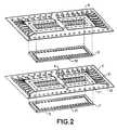
- a plurality of such pellets and their connection meansare stacked one above the other, as illustrated in the exploded view of Figure 2 for two tablets.
- Figure 3ashows a sectional view of the stack according to the invention, produced along an axis XX illustrated in FIG. 1, normal on sides 12 and 14 of the pellets.
- the semiconductor chip 1provided with its connection means, namely tracks (31 and 41), studs (32) and conductors (16).
- This setconstitutes for example the top layer of a stack of five pellets, the others pellets being identified 5, 51, 52 and 53, each provided with its means connection carried by an insulating film (6, 61, 62 and 63).
- the setis secured using an insulating material 7, for example a resin epoxy.
- the insulating materials (7, 3, 6, 61-63)have not been hatched although seen in section.
- the stackis then cut along a line ZZ of the Figure 1 passing through the cutout 23, between the central part 4 and the frame 3; the cutting lines are illustrated in zz in FIG. 3a.
- the frames 3are removed and the conductors 16 are flush the faces of the stack.
- Figure 3bis a section similar to that of Figure 3a but performed perpendicular to the previous one, along an axis YY of Figure 1. This view illustrates the clearance on side 11 of semiconductor pads.
- the zz cut made on side 11can either be made at flush with the patch 1, ie substantially in the middle of the cutout 23, as illustrated in the figures; in the latter case, the stack must be later polished so that the edge of the pellets on this face of the stack to allow good thermal evacuation by conduction.
- the slices of the pellets but a certain thicknessis left insulating material 7, which is thin enough not to interfere the thermal evacuation but which remains sufficient to ensure the mechanical protection and tightness of the stack which can be required in some applications.
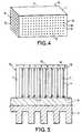
- FIG. 4represents a perspective view of the stack, after cutting along line ZZ in figure 1.
- the stacktherefore appears as a block 70, formed of dielectric material 7 on certain faces of which the conductors 16 and 18.
- the face of the stackhas been designated by 71 which corresponds to side 11 of the pads 1, par 72 that which corresponds to their side 12, by 73 that which corresponds to their side 13 and by 74 that which corresponds to their side 14.
- face 72therefore the conductors 16, directly connecting the pads 15 of the pads to the tracks 31 of the frame before its cutting.
- Face 71which is not visible on the figure, is devoid of conductors.
- conductorssuch as 16 directly connected to the pads of the pads and conductors such as 18, which are connected to the pads 15 located on the side 11 via tracks 41 of the central part 4.
- This figureshows the conductors 16 and 18 aligned in rows and columns, regularly spaced; that of course is by way of example and the distribution of conductors can be adapted according to the applications.
- FIG. 5represents a sectional view of the stack according to the invention, connected to thermal evacuation means.
- the stack 70 according to the inventionis formed by example by eight pads such as 1, each provided with the part central 4 of film 2; the pads of the pads 1 are connected either directly by conductors 16 (shown in dotted lines) on face 73 of the stack, either indirectly by the conductors 17, 18 and the part central 4 on this same face 73.
- the studs padscan also be connected to the faces 72 and 74 of the stack, not visible in the section of FIG. 5.
- the face 71 having no connections electric and on which the pads are flush,is connected to means of thermal evacuation.
- these meansare for example constituted by a radiator 9, comprising fins and made of a good material heat conductor and preferably electrical insulator.
- the stack 70can be connected directly to the radiator 9 if the coefficients of thermal expansion of elements 70 and 9 are sufficiently close; in the case where the pellets 1 are made of silicon for example, the radiator 9 can be made of aluminum nitride, of carbide silicon or diamond. Otherwise, the stack 70 can be connected to the radiator 9 via a layer 8, as shown in Figure 5, layer 8 providing thermo-mechanical adaptation necessary and being for example carried out in one of the materials mentioned above. Elements 70, 9 and possibly 8 are, as necessary, fixed to each other using a very thin layer of glue.
- Figure 6shows a partial perspective view of a printed circuit carrying several stacks according to the invention.
- a printed circuit 80carrying for example four stacks, marked 82, 83, 84 and 85.
- Each of the stacksis arranged on the printed circuit by its face 73 so that it can connect face 71 to thermal evacuation means (not shown) as illustrated in Figure 5; the ends of conductors connecting the pads of the pads are flush on the faces 72, 73 and 74 of each of the blocks.
- FIG. 7represents an exemplary embodiment of the interconnection of the pellets forming a stack 70, this interconnection being carried out on the lateral surfaces of the stack.
- stack 70comprising the faces 72 and 73 on which the connected conductors are flush, directly or not, with the pads of the pellets; face 71 on which are flush with the pads themselves is located, in this figure, below.
- the conductors flush with the faces 72 or 73are indistinctly marked F, whether they correspond to conductors 16 or to the conductors 18 of the previous figures.
- Stacking 70further comprises studs 81, called stacking studs, making it possible to connect it to external circuits.
- the F conductorsare both interconnected with each other, when necessary, and connected to the studs stacking 81, also when necessary, using connections C.
- the stacking pads 81have been illustrated on one side. parallel to the pads 1, in the vicinity of the face 71, but it is understood that they can occupy any position on the faces of the stack, except on face 71.
- Each of the C connectionscan be made in the following way: following: we metallize all of the faces of the stack 70, then each of the connections C is formed by two laser engravings destroying locally the metal layer up to the insulating layer, achieving thus the electrical insulation of connection C from the rest of the layer metallic.
- the stacking pads 81can advantageously be made by the same laser engraving technique.
- Another method of making connections Cconsists in first make grooves in the stack, according to the selected design for connections C, at the level where the conductors F are flush, so as to release the end of the latter; then we deposit a electrically conductive layer (metal for example) on the whole stacking, faces and grooves; finally, we remove the layer conductive of the flat surfaces of the stack (by polishing or by laser for example), so that it only remains in the grooves where it makes the desired connections.
- a electrically conductive layermetal for example
- FIG. 8represents an alternative embodiment of the means connecting a pad, used in the device according to the invention.
- This figureis a partial top view of a pellet 1 and of its connection means, carried by the insulating film comprising the central part 4 and the frame 3.
- the means connectionare carried no longer by a single insulating film but by a multilayer film, formed from a plurality of electrically layers conductive (two, for example) separated by insulating layers, so as to allow more freedom in the routing of the tracks the central part.
- the frame 3 providedis partially shown of its tracks 31, as well as the chip 1 provided with its studs 15, covered with the central part 4 which is connected to the frame 3 by tabs 24 and 25. Note that these tabs are not necessarily two in number or of the same width and that it is not not essential that they are arranged one opposite the other.
- the multilayer constitution of the central part 4makes it possible to cross tracks run by this last part, so as to connect the pads 15 on the side 11 of the patch to any one on the other sides of the frame 3.
- three tracks 41substantially straight and allowing the studs 15 to emerge via the conductors 17 and 18 on the face 73 of the stack when finished; there is also a track 42, in dotted lines because formed in the lower conductive layer, which allows to connect between them two studs 43 of part 4 formed, them, on the upper layer and connected to track 42 by any known means (metallized holes at through the central insulating layer for example);
- one of the studs 43is located for example at the bottom left of part 4 and connected to stud 15 which faces him; the other pad 43 is located at the top right of this same part 4 and is connected to a track 31 which substantially faces it.
- the pads and tracks of the central part 4are formed in one of the conductive layers and are isolated from the rest of the layers.
- Figures 9a and 9bshow other variants of realization of the connection means of the pellets.
- FIG. 9arepresents a fractional section view of a stack according to the invention, in which only one is shown patch 1 and its connection means, embedded in the material insulator 7. For clarity of the drawing, the latter has not been hatched well as seen in section.
- the stackingis carried out as described above, except for the position relative connection means and the corresponding pad: in indeed, the film and especially its central part, now marked 40, is disposed under the patch 1, that is to say against its face rear 19 which does not carry the connection pads 15.
- the pad 1is therefore fixed on the central part 40, where appropriate by the intermediary an insulating adhesive.
- some of the pads 15are directly connected to the faces of the stack (by conductors 16), for example the face 73 in the figure.
- the studs 15 located on the side 11 of the patchare indirectly connected to these same faces, by through tracks carried by the central part, here marked 44 and arranged on an insulating layer 49, and the intermediate of conductors 17 and 18.
- the face 71is therefore devoid of connections.
- the central part 40comprises at in addition to a layer 48 of a material which is a good conductor of heat, copper for example, placed on the insulating layer 49 opposite the tracks 44.
- the central part 40 and particularly the conductive layer 48which is exposed on the face 71 and not directly on side 11, because of the conductors 17.
- a good thermal evacuationcan also be ensured here, subject to to choose the materials constituting part 40 appropriately as well as its dimensions, which then depend only on the only thermal parameters.
- Figure 9bis a view similar to that of Figure 9a, which illustrates an alternative embodiment of the previous figure in which the central part is multilayer, similar to what is described figure 8.
- the part 40here comprises four layers: two conductive layers 45 and 47 separated by an insulating layer 46 and the conductive layer 48.
- One of the conductive layers, for example layer 45is placed on the face 16 of the patch 1 and by example fixed by an insulating adhesive.
- Conductors 17 and 18are connected to studs formed in layer 45.
- some of these pads of layer 45are linked together by tracks also formed in layer 45, some others are interconnected by tracks formed in the layer 47 and are connected to this layer 47 through layer 46 by all known means, metallized holes for example.
- At layer 47is fixed the thermally conductive layer 48, if necessary by through an insulating adhesive 50.
- heat sinksmade of a material that conducts heat well, crossing the layers separating the layer 48 from the rear face 19 and the if necessary electrically isolated from these layers, improving the thermal conduction through part 40 and therefore the evacuation of the heat.
- thermal evacuationit is done either directly by the edge of the pellets (preferably, the large side of the rectangle), either by means of connection of the pads, of which the dimensioning and the constituent materials can then be adapted to the thermal function assigned to them, the latter locally having no constraints related to electrical connections fill.
Landscapes
- Engineering & Computer Science (AREA)
- Microelectronics & Electronic Packaging (AREA)
- Power Engineering (AREA)
- Computer Hardware Design (AREA)
- Physics & Mathematics (AREA)
- Condensed Matter Physics & Semiconductors (AREA)
- General Physics & Mathematics (AREA)
- Manufacturing & Machinery (AREA)
- Semiconductor Integrated Circuits (AREA)
- Cooling Or The Like Of Semiconductors Or Solid State Devices (AREA)
- Wire Bonding (AREA)
Description
Translated fromFrenchLa présente invention a pour objet un procédé et un dispositifd'encapsulation en trois dimensions de pastilles semi-conductrices,chacune des pastilles contenant par exemple un composantélectronique, un circuit intégré, ou un capteur, cette encapsulationvisant à présenter une bonne évacuation thermique par conduction.The present invention relates to a method and a devicethree-dimensional encapsulation of semiconductor wafers,each tablet containing for example a componentelectronic, an integrated circuit, or a sensor, this encapsulationaiming to present a good thermal evacuation by conduction.
La réalisation des systèmes électroniques actuels, tant civilsque militaires, doit tenir compte d'exigences de plus en plus grandes decompacité, du fait du nombre de plus en plus élevé de circuits mis enoeuvre.The realization of current electronic systems, both civilthat military personnel must take into account the increasing demands ofcompactness, due to the increasing number of circuits implementedartwork.
Dans cette recherche de plus grande compacité, il a déjà étéproposé de réaliser des empilements en trois dimensions de circuitsintégrés comme par exemple décrit dans le brevet américainn° 4.706.166. Selon cette réalisation, les pastilles sont disposées surun circuit imprimé, accolées les unes aux autres perpendiculairementau circuit imprimé; les plots de connexion de chacune des pastillessont ramenés sur un même bord de la pastille; ce côté est disposé surle circuit imprimé et les connexions avec ce dernier y sont réalisées.Toutefois, cet arrangement présente des limitations notamment liées aunombre de plots qu'il est matériellement possible de disposer sur unseul côté d'une pastille semi-conductrice; en outre, il est onéreux dufait que les pastilles ne sont pas standard (la disposition des plots doitêtre modifiée); de plus, les connexions ainsi réalisées sont peuaccessibles et de plus non visibles, ce qui en limite l'utilisation. Enfin,dans certaines applications peut se poser un problème d'évacuationthermique. Classiquement, celle-ci peut s'effectuer par conduction ou convexion ; dans la réalisation décrite ci-dessus, l'évacuation thermiquepar conduction est limitée du fait qu'elle ne peut s'effectuer que par lesplots de connexion électrique au circuit imprimé, plots qui sont desection réduite et en nombre réduit; un tel dispositif exige donc, pourfonctionner de façon satisfaisante, un refroidissement par convexion.Toutefois, dans certaines applications, un tel refroidissement estdifficile voire impossible à mettre en oeuvre, notamment dans lesapplications avioniques ou spatiales.In this search for greater compactness, it has already beenproposed to make three-dimensional stacks of circuitsintegrated as for example described in the American patentNo. 4,706,166. According to this embodiment, the pellets are arranged ona printed circuit, joined to each other perpendicularlyto the printed circuit; the connection pads of each of the padsare brought to the same edge of the patch; this side is arranged onthe printed circuit and the connections with the latter are made there.However, this arrangement has limitations notably related to thenumber of pads that it is physically possible to have on asingle side of a semiconductor chip; in addition, it is expensive tofact that the pads are not standard (the arrangement of the pads mustbe modified); moreover, the connections thus made are fewaccessible and also not visible, which limits its use. Finally,in some applications there may be an evacuation problemthermal. Conventionally, this can be done by conduction orconvection; in the embodiment described above, the thermal evacuationby conduction is limited because it can only be done bypads for electrical connection to the printed circuit, pads which arereduced section and reduced number; such a device therefore requires, foroperate satisfactorily, convection cooling.However, in some applications, such cooling isdifficult or even impossible to implement, especially inavionics or space applications.
Il est par ailleurs connu de l'article "3-D Interconnection forUltra-Dense Multichip Modules" de C. Val et al. paru dans IEEETransactions on Components, Hybrids and Manufacturing Technology,vol. 13, N° 4, pages 814-821, 1990, une technologie d'empilement etd'interconnexion de pastilles semi-conductrices, ainsi que du document"Patents Abstracts of Japan, vol. 13, n° 366 (E-806), 15th August 1989,JP-A- 01 123 427, une méthode pour positionner d'un seul côté lesbroches de connexion d'un boítier pour pastille semi-conductrice.It is also known from the article "3-D Interconnection forUltra-Dense Multichip Modules "by C. Val et al. Published in IEEETransactions on Components, Hybrids and Manufacturing Technology,flight. 13, No. 4, pages 814-821, 1990, a stacking technology andinterconnection of semiconductor pads, as well as the document"Patents Abstracts of Japan, vol. 13, n ° 366 (E-806), 15th August 1989,JP-A- 01 123 427, a method for positioning on one side theconnection pins of a case for semiconductor chip.
La présente invention a pour objet une encapsulation en troisdimensions de circuits intégrés qui permette une bonne évacuationthermique par conduction, tout en restant peu onéreuse.The present invention relates to an encapsulation in threedimensions of integrated circuits which allow good evacuationthermal by conduction, while remaining inexpensive.
A cet effet, les plots de chacune des pastilles sont prolongés àl'aide de moyens de connexion vers, au maximum, trois côtés de lapastille, dégageant de la sorte le quatrième côté. Les pastilles sontempilées les unes sur les autres, puis reliées à des moyensd'évacuation thermique par leur quatrième côté, permettant ainsi unrefroidissement par conduction.For this purpose, the pads of each of the pellets are extended tousing connection means to, at most, three sides of thelozenge, thereby clearing the fourth side. The pastilles arestacked on top of each other, then connected to meansof thermal evacuation by their fourth side, thus allowing aconduction cooling.
Plus précisément, l'invention a pour objet un procédéd'encapsulation en trois dimensions de pastilles semi-conductrices telque défini par la revendication 1. Elle a également pour objet undispositif d'encapsulation en trois dimensions de pastilles semi-conductricestel que défini par la revendication 11.More specifically, the subject of the invention is a methodthree-dimensional encapsulation of semiconductor wafers such asas defined by
D'autres objets, particularités et résultats de l'inventionressortiront de la description suivante, donnée à titre d'exemple etillustrée par les dessins annexés, qui représentent:
- la figure 1, une vue de dessus d'une pastille et de ses moyensde connexion entrant dans la formation du dispositif selon l'invention ;
- la figure 2, une vue éclatée et partielle du dispositif selonl'invention ;
- les figures 3a et 3b, deux vues en coupe du dispositif selonl'invention ;
- la figure 4, une vue en perspective de l'empilement réaliséselon l'invention ;
- la figure 5, une vue en coupe du dispositif selon l'inventionrelié à des moyens d'évacuation thermique ;
- la figure 6, une vue en perspective fractionnaire d'un circuitimprimé portant plusieurs dispositifs selon l'invention ;
- la figure 7, un exemple de réalisation de l'interconnexion despastilles ;
- la figure 8, une variante de réalisation des moyens deconnexion d'une pastille utilisés dans le dispositif selon l'invention ;
- les figures 9a et 9b, d'autres variantes de réalisation desmoyens de connexion d'une pastille.
- Figure 1, a top view of a patch and its connection means used in the formation of the device according to the invention;
- Figure 2, an exploded and partial view of the device according to the invention;
- Figures 3a and 3b, two sectional views of the device according to the invention;
- Figure 4, a perspective view of the stack produced according to the invention;
- Figure 5, a sectional view of the device according to the invention connected to thermal evacuation means;
- FIG. 6, a fractional perspective view of a printed circuit carrying several devices according to the invention;
- FIG. 7, an exemplary embodiment of the interconnection of the pads;
- Figure 8, an alternative embodiment of the connection means of a pad used in the device according to the invention;
- Figures 9a and 9b, other alternative embodiments of the connection means of a pad.
Sur ces différentes figures, les mêmes références se rapportentaux mêmes éléments. En outre, pour la clarté des dessins, l'échelleréelle n'a pas été respectée.In these different figures, the same references relateto the same elements. In addition, for the sake of clarity, the scalewas not observed.
La figure 1 représente donc une vue de dessus d'une pastille etde ses moyens de connexions.FIG. 1 therefore represents a top view of a pellet andof its connection means.
Sur cette figure, on a représenté une pastille semi-conductrice1 dans laquelle peut être réalisé tout composant électronique, circuitintégré ou capteur. La pastille est par exemple rectangulaire et sesquatre côtés sont repérés respectivement 11, 12, 13 et 14. La facesupérieure de cette pastille, visible sur la figure, porte des plots 15d'entrées sorties électriques de l'élément contenu dans la pastille,disposés par exemple sur ses quatre côtés.This figure shows a
Selon l'invention, on relie chacun des plots 15 à des moyens deconnexion permettant de diriger ces connexions vers au maximum troiscôtés de la pastille, dégageant de la sorte le quatrième côté, le côté 11dans l'exemple de la figure 1. Les moyens de connexion comportent unfilm isolant 2, de préférence mince, réalisé par exemple en polyimide ou polyester, et dans lequel est pratiquée une découpe 23, laissantsubsister un cadre 3 et une partie centrale 4 reliée au cadre par deuxlanguettes 24 et 25. Les bords du cadre 3, par exemple deux de sesbords, comportent des trous 21, par exemple rectangulaires ou oblongs,permettant le guidage et le positionnement précis du film 2 sur unemachine de câblage automatique par exemple. Le cadre 3 comporte enoutre un ensemble de plots 32 disposés au voisinage de la périphériedu cadre 3 et ce, selon l'invention, sur trois côtés au maximum, laissantle côté situé du côté 11 de la pastille 1 libre. Ces plots 32 sont reliés aubord intérieur 22 du cadre 3 par des dépôts conducteurs, ou pistes, 31réalisés sur le film 2. Les plots 32 sont utilisés par exemple pour le testet le déverminage des pastilles semiconductrices, avant leurempilement. La partie centrale 4 comporte également des pistesrepérées 41, rectilignes ou non.According to the invention, each of the
Les plots 15 situés sur les côtés 12, 13 et 14 de la pastille 1sont reliés directement aux pistes 31 du cadre 3, au voisinage du bordintérieur 22, à l'aide d'un conducteur 16, qui peut être un fil commereprésenté sur la figure ou un ruban. Ceux des plots 15 qui sont situéssur le côté 11 sont reliés par des conducteurs 17 (fils ou rubans) à uneextrémité des pistes 41 portées par la partie centrale 4, l'autre extrémitéde ces pistes étant reliée par des conducteurs 18 (fils ou rubans) auxpistes 31 situées par exemple sur le côté du cadre 3 qui est à l'opposédu côté 11. Ces opérations peuvent typiquement être réalisées à l'aidede machines de câblage automatique, utilisées par exemple pour câblerles pastilles semi-conductrices dans leur boítier.The
Il apparaít ainsi que l'un des côtés de la pastille 1 (le côté 11) aété dégagé de toute connexion. Ce côté dégagé est utilisable pourl'évacuation thermique par conduction, comme expliqué plus loin. Danscette optique, il est préférable de dégager un grand côté du rectangle.Mais, bien entendu, un ou plusieurs autres côtés peuvent êtreégalement dégagés, en fonction des utilisations.It appears that one of the sides of the patch 1 (side 11) hasbeen cleared of any connection. This clear side can be used forthermal evacuation by conduction, as explained below. InWith this in mind, it is preferable to clear a large side of the rectangle.But, of course, one or more other sides can bealso cleared, depending on the uses.
Selon l'invention, une pluralité de telles pastilles et leursmoyens de connexions sont empilés les uns au dessus des autres,comme illustré sur la vue éclatée de la figure 2 pour deux pastilles.According to the invention, a plurality of such pellets and theirconnection means are stacked one above the other,as illustrated in the exploded view of Figure 2 for two tablets.
Sur la figure 2, on retrouve la pastille semi-conductrice 1 et sesmoyens de connexion, formés par le film isolant 2 et ses pistes et plotsconducteurs 31, 41 et 32. Sur cette figure 2, les conducteurs 16, 17, et18 n'ont pas été représentés. On a représenté également une secondepastille semi-conductrice, repérée 5, à laquelle sont associés desmoyens de connexion, constitués de façon analogue à ceux de lapastille 1 par un film diélectrique 6 comportant un cadre et une partiecentrale, sur lesquels sont disposés des pistes et des plots. Leséléments 1, 2, 5 et 6 sont empilés les uns sur les autres et les pastilles1 et 5 sont disposées de sorte que leurs côtés dégagés (11 pour lapastille 1, 51 pour la pastille 5) soient situés du même côté del'empilement ainsi réalisé.In Figure 2, we find the
La figure 3a représente une vue en coupe de l'empilementselon l'invention, réalisée selon un axe XX illustré sur la figure 1,normal aux côtés 12 et 14 des pastilles.Figure 3a shows a sectional view of the stackaccording to the invention, produced along an axis XX illustrated in FIG. 1,normal on
Sur cette figure, on retrouve la pastille semi-conductrice 1munie de ses moyens de connexion, à savoir pistes (31 et 41), plots(32) et conducteurs (16). Cet ensemble constitue par exemple lacouche supérieure d'un empilement de cinq pastilles, les autrespastilles étant repérées 5, 51, 52 et 53, chacune munie de ses moyensde connexion portés par un film isolant (6, 61, 62 et 63). L'ensemble estsolidarisé à l'aide d'un matériau isolant 7, par exemple une résineépoxy. Pour la clarté de la figure, les matériaux isolants (7, 3, 6, 61-63)n'ont pas été hachurés bien que vus en coupe.In this figure, we find the
L'empilement est ensuite découpé selon une ligne ZZ de lafigure 1 passant dans la découpe 23, entre la partie centrale 4 et lecadre 3 ; les lignes de découpage sont illustrées en zz sur la figure 3a. De la sorte, les cadres 3 sont enlevés et les conducteurs 16 affleurentles faces de l'empilement.The stack is then cut along a line ZZ of theFigure 1 passing through the
La figure 3b est une coupe analogue à celle de la figure 3amais réalisée perpendiculairement à la précédente, selon un axe YY dela figure 1. Cette vue permet d'illustrer le dégagement du côté 11 despastilles semi-conductrices.Figure 3b is a section similar to that of Figure 3abut performed perpendicular to the previous one, along an axis YY ofFigure 1. This view illustrates the clearance on
Sur cette figure, on distingue les côtés 11 et 13 de la pastillesemi-conductrice 1, recouverte de la partie centrale 4 du film isolant etentourée du cadre 3 de ce même film. On voit que les plots 15 de lapastille qui sont situés du côté 11 sont reliés par les conducteurs 17aux pistes 41 portées par la partie centrale 4 ; ces pistes 41 sont reliéesà l'autre de leurs extrémités par les conducteurs 18 aux pistes 31 ducadre 3. On a représenté en pointillés les plots 15 situés du côté 13 dela pastille, qui sont reliés directement par les conducteurs 16 à d'autrespistes 31 du cadre 3.In this figure, there are
Comme précédemment, on a représenté le matériau 7 desolidarisation et les lignes de découpe zz correspondant à la ligne ZZde la figure 1. La découpe zz effectuée du côté 11 peut soit être faite auras de la pastille 1, soit sensiblement au milieu de la découpe 23,comme illustré sur les figures; dans ce dernier cas, l'empilement doitêtre ultérieurement poli de façon à faire affleurer la tranche despastilles sur cette face de l'empilement pour permettre une bonneévacuation thermique par conduction.As before, the
Dans une variante de réalisation, on ne fait pas affleurer lestranches des pastilles mais on laisse subsister une certaine épaisseurdu matériau isolant 7, qui soit suffisamment fine pour ne pas gênerl'évacuation thermique mais qui reste suffisante pour assurer laprotection mécanique et l'étanchéité de l'empilement qui peuvent êtrenécessaires dans certaines applications.In an alternative embodiment, theslices of the pellets but a certain thickness is leftinsulating
La figure 4 représente une vue en perspective de l'empilement,après découpe le long de la ligne ZZ de la figure 1.FIG. 4 represents a perspective view of the stack,after cutting along line ZZ in figure 1.
L'empilement apparaít donc comme un bloc 70, formé dumatériau diélectrique 7 sur certaines faces duquel affleurent lesconducteurs 16 et 18.The stack therefore appears as a
Plus précisément, on a désigné par 71 la face de l'empilementqui correspond au côté 11 des pastilles 1, par 72 celle qui correspond àleur côté 12, par 73 celle qui correspond à leur côté 13 et par 74 cellequi correspond à leur côté 14. Sur la face 72 affleurent donc lesconducteurs 16, reliant directement les plots 15 des pastilles aux pistes31 du cadre avant sa découpe. La face 71, qui n'est pas visible sur lafigure, est dépourvue de conducteurs. Sur la face 73 affleurent à la foisdes conducteurs tels que 16 reliés directement aux plots des pastilleset des conducteurs tels que 18, qui sont reliés aux plots 15 situés ducôté 11 par l'intermédiaire des pistes 41 de la partie centrale 4.More precisely, the face of the stack has been designated by 71which corresponds to
On a représenté sur cette figure les conducteurs 16 et 18alignés selon des lignes et des colonnes, régulièrement espacés; celal'est bien entendu à titre d'exemple et la répartition des conducteurspeut être adaptée selon les applications.This figure shows the
La figure 5 représente une vue en coupe de l'empilement selonl'invention, relié à des moyens d'évacuation thermique.FIG. 5 represents a sectional view of the stack according tothe invention, connected to thermal evacuation means.
Sur cette figure, l'empilement 70 selon l'invention est formé parexemple par huit pastilles telles que 1, chacune munie de la partiecentrale 4 du film 2 ; les plots des pastilles 1 sont reliés soit directementpar les conducteurs 16 (représentées en pointillés) à la face 73 del'empilement, soit indirectement par les conducteurs 17, 18 et la partiecentrale 4 à cette même face 73. Comme expliqué ci-dessus, les plotsdes pastilles peuvent être également reliés aux faces 72 et 74 del'empilement, non visibles sur la coupe de la figure 5.In this figure, the
Selon l'invention, la face 71 ne comportant pas de connexionsélectriques et sur laquelle affleurent les pastilles, est reliée à des moyens d'évacuation thermique. Dans le mode de réalisationreprésenté sur la figure, ces moyens sont par exemple constitués parun radiateur 9, comportant des ailettes et réalisé en un matériau bonconducteur de la chaleur et de préférence isolant électrique.According to the invention, the
L'empilement 70 peut être relié directement au radiateur 9 si lescoefficients de dilatation thermique des éléments 70 et 9 sontsuffisamment proches; dans le cas où les pastilles 1 sont en siliciumpar exemple, le radiateur 9 peut être en nitrure d'aluminium, en carburede silicium ou en diamant. Dans le cas contraire, l'empilement 70 peutêtre relié au radiateur 9 par l'intermédiaire d'une couche 8, commereprésenté sur la figure 5, la couche 8 assurant l'adaptation thermo-mécaniquenécessaire et étant par exemple réalisée dans l'un desmatériaux mentionnés ci-dessus. Les éléments 70, 9 et éventuellement8 sont, en tant que besoin, fixés les uns aux autres à l'aide d'une trèsmince couche de colle.The
La figure 6 représente une vue en perspective partielle d'uncircuit imprimé portant plusieurs empilements selon l'invention.Figure 6 shows a partial perspective view of aprinted circuit carrying several stacks according to the invention.
On a donc illustré un circuit imprimé 80 portant par exemplequatre empilements, repérés 82, 83, 84 et 85. Chacun des empilementsest disposé sur le circuit imprimé par sa face 73 de sorte à pouvoirrelier la face 71 à des moyens d'évacuation thermique (nonreprésentés) comme illustré sur la figure 5; les extrémités desconducteurs connectant les plots des pastilles affleurent sur les faces72, 73 et 74 de chacun des blocs.We have therefore illustrated a printed
La figure 7 représente un exemple de réalisation del'interconnexion des pastilles formant un empilement 70, cetteinterconnexion étant réalisée sur les surfaces latérales de l'empilement.FIG. 7 represents an exemplary embodiment ofthe interconnection of the pellets forming a
Sur cette figure, on retrouve l'empilement 70 comportant lesfaces 72 et 73 sur lesquelles affleurent les conducteurs reliés,directement ou non, aux plots des pastilles; la face 71 sur laquelle affleurent les pastilles elles-mêmes est située, sur cette figure,dessous. Les conducteurs affleurant les faces 72 ou 73 sontindistinctement repérés F, qu'ils correspondent aux conducteurs 16 ouaux conducteurs 18 des figures précédentes. L'empilement 70comporte en outre des plots 81, dits plots d'empilement, permettant dele connecter à des circuits extérieurs. Les conducteurs F sont à la foisinterconnectés entre eux, quand nécessaire, et reliés aux plotsd'empilement 81, également quand nécessaire, à l'aide de connexionsC. A titre d'exemple, on a illustré les plots d'empilement 81 sur une faceparallèle aux pastilles 1, au voisinage de la face 71, mais il est entenduqu'ils peuvent occuper toute position sur les faces de l'empilement, saufsur la face 71.In this figure, we find the
Chacune des connexions C peut être réalisée de la façonsuivante: on métallise l'ensemble des faces de l'empilement 70, puison forme chacune des connexions C par deux gravures laser détruisantlocalement la couche métallique jusqu'à la couche isolante, réalisantainsi l'isolation électrique de la connexion C du reste de la couchemétallique. Les plots d'empilement 81 peuvent être avantageusementréalisés par la même technique de gravure laser.Each of the C connections can be made in the following way:following: we metallize all of the faces of the
Une autre méthode de réalisation des connexions C consiste àréaliser d'abord des rainures dans l'empilement, selon le dessin retenupour les connexions C, au niveau où les conducteurs F affleurent, desorte à dégager l'extrémité de ces derniers; puis on dépose unecouche électriquement conductrice (métal par exemple) sur l'ensemblede l'empilement, faces et rainures; enfin, on enlève la coucheconductrice des surfaces planes de l'empilement (par polissage ou parlaser par exemple), de sorte à ne la laisser subsister que dans lesrainures où elle réalise les connexions recherchées.Another method of making connections C consists infirst make grooves in the stack, according to the selected designfor connections C, at the level where the conductors F are flush,so as to release the end of the latter; then we deposit aelectrically conductive layer (metal for example) on the wholestacking, faces and grooves; finally, we remove the layerconductive of the flat surfaces of the stack (by polishing or bylaser for example), so that it only remains in thegrooves where it makes the desired connections.
La figure 8 représente une variante de réalisation des moyensde connexion d'une pastille, utilisés dans le dispositif selon l'invention.FIG. 8 represents an alternative embodiment of the meansconnecting a pad, used in the device according to the invention.
Cette figure est une vue partielle de dessus d'une pastille 1 etde ses moyens de connexion, portés par le film isolant comportant lapartie centrale 4 et le cadre 3. Dans ce mode de réalisation, les moyensde connexion sont portés non plus par un film isolant unique mais parun film multicouche, formé d'une pluralité de couches électriquementconductrices (deux, par exemple) séparées par des couches isolantes,de façon à permettre plus de liberté au niveau du routage des pistes dela partie centrale.This figure is a partial top view of a
Plus précisément, on a représenté partiellement le cadre 3 munide ses pistes 31, ainsi que la pastille 1 munie de ses plots 15,recouverte de la partie centrale 4 qui est reliée au cadre 3 par deslanguettes 24 et 25. On notera que ces languettes ne sont pasnécessairement au nombre de deux ni de même largeur et qu'il n'estpas indispensable qu'elles soient disposées l'une en face de l'autre.More specifically, the
La constitution multicouche de la partie centrale 4 permet deréaliser des croisements des pistes portées par cette dernière partie, defaçon à relier les plots 15 du côté 11 de la pastille à l'un quelconquedes autres côtés du cadre 3. A titre d'exemple, on a représenté sur lafigure, disposées sur la partie centrale 4, trois pistes 41 sensiblementrectilignes et permettant de faire émerger les plots 15 via lesconducteurs 17 et 18 sur la face 73 de l'empilement une fois terminé;on a représenté également une piste 42, en traits pointillés parce queformée dans la couche conductrice inférieure, qui permet de relier entreeux deux plots 43 de la partie 4 formés, eux, sur la couche supérieureet reliés à la piste 42 par tous moyens connus (trous métallisés àtravers la couche centrale isolante par exemple); l'un des plots 43 estsitué par exemple en bas à gauche de la partie 4 et relié au plot 15 quilui fait face; l'autre plot 43 est situé en haut à droite de cette mêmepartie 4 et est relié à une piste 31 qui lui fait sensiblement face. Bienentendu, les plots et pistes de la partie centrale 4 sont formés dansl'une des couches conductrices et sont isolés du reste des couches.The multilayer constitution of the
Les figures 9a et 9b représentent d'autres variantes deréalisation des moyens de connexion des pastilles.Figures 9a and 9b show other variants ofrealization of the connection means of the pellets.
La figure 9a représente une vue en coupe fractionnaire d'unempilement selon l'invention, dans laquelle on a représenté une seulepastille 1 et ses moyens de connexion, enrobés dans le matériauisolant 7. Pour la clarté du dessin, ce dernier n'a pas été hachuré bienque vu en coupe.FIG. 9a represents a fractional section view of astack according to the invention, in which only one is shown
Selon cette variante de réalisation, l'empilement est réalisécomme décrit précédemment, sauf en ce qui concerne la positionrelative des moyens de connexion et de la pastille correspondante: eneffet, le film et tout particulièrement sa partie centrale, maintenantrepérée 40, est disposé sous la pastille 1, c'est-à-dire contre sa facearrière 19 qui ne porte pas les plots de connexion 15. La pastille 1 estdonc fixée sur la partie centrale 40, le cas échéant par l'intermédiaired'une colle isolante. Comme précédemment, certains des plots 15 sontreliés directement aux faces de l'empilement (par des conducteurs 16),par exemple la face 73 sur la figure. Au contraire, les plots 15 situés ducôté 11 de la pastille sont reliés indirectement à ces mêmes faces, parl'intermédiaire de pistes portées par la partie centrale, ici repérées 44 etdisposées sur une couche isolante 49, et l'intermédiaire desconducteurs 17 et 18. La face 71, comme précédemment, est doncdépourvue de connexions. Enfin, la partie centrale 40 comporte enoutre une couche 48 d'un matériau bon conducteur de la chaleur, ducuivre par exemple, disposé sur la couche isolante 49 à l'opposé despistes 44.According to this alternative embodiment, the stacking is carried outas described above, except for the positionrelative connection means and the corresponding pad: inindeed, the film and especially its central part, nowmarked 40, is disposed under the
Dans ce mode de réalisation, c'est la partie centrale 40 etparticulièrement la couche conductrice 48, qui affleure sur la face 71 etnon directement le côté 11, à cause des conducteurs 17. Toutefois, unebonne évacuation thermique peut ici aussi être assurée, sous réservede choisir de façon appropriée les matériaux constituant la partie 40ainsi que ses dimensions, qui ne dépendent alors que des seulsparamètres thermiques.In this embodiment, it is the
La figure 9b est une vue analogue à celle de la figure 9a, quiillustre une variante de réalisation de la figure précédente dans laquellela partie centrale est multicouche, de façon analogue à ce qui est décritfigure 8.Figure 9b is a view similar to that of Figure 9a, whichillustrates an alternative embodiment of the previous figure in whichthe central part is multilayer, similar to what is describedfigure 8.
Plus précisément, la partie 40 comporte ici quatre couches:deux couches conductrices 45 et 47 séparées par une couche isolante46 et la couche conductrice 48. L'une des couches conductrices, parexemple la couche 45, est disposée sur la face 16 de la pastille 1 et parexemple fixée par une colle isolante. Les conducteurs 17 et 18 sontreliés à des plots formés dans la couche 45. De façon analogue à cequi est décrit sur la figure 8, certains de ces plots de la couche 45 sontreliés entre eux par des pistes également formées dans la couche 45,certains autres sont reliés entre eux par des pistes formées dans lacouche 47 et sont reliés à cette couche 47 à travers la couche 46 partous moyens connus, trous métallisés par exemple. A la couche 47 estfixée la couche thermiquement conductrice 48, le cas échéant parl'intermédiaire d'une colle isolante 50.More specifically, the
Dans l'une ou l'autre des variantes représentées sur les figures9a et 9b, il est possible d'ajouter des puits thermiques (nonreprésentés), réalisés en un matériau bon conducteur de la chaleur,traversant les couches séparant la couche 48 de la face arrière 19 et lecas échéant électriquement isolés de ces couches, améliorant laconduction thermique à travers la partie 40 et donc l'évacuation de lachaleur.In one or other of the variants shown in the figures9a and 9b, it is possible to add heat sinks (notshown), made of a material that conducts heat well,crossing the layers separating the
Il a été ainsi décrit un dispositif d'encapsulation etd'interconnexion en trois dimensions de pastilles semi-conductrices, quiest à la fois adapté au refroidissement par conduction et peu onéreux.There has thus been described an encapsulation device andthree-dimensional interconnection of semiconductor wafers, whichis both suitable for conduction cooling and inexpensive.
En effet, en ce qui concerne l'évacuation thermique, elle se faitsoit directement par la tranche des pastilles (de préférence, le grandcôté du rectangle), soit par les moyens de connexion des pastilles, dont le dimensionnement et les matériaux constitutifs peuvent alors êtreadaptés à la fonction thermique qui leur est affectée, ces derniersn'ayant localement pas de contraintes liées à la connectique électriqueà remplir.Indeed, with regard to thermal evacuation, it is doneeither directly by the edge of the pellets (preferably, the largeside of the rectangle), either by means of connection of the pads, of whichthe dimensioning and the constituent materials can then beadapted to the thermal function assigned to them, the latterlocally having no constraints related to electrical connectionsfill.
Quant aux coûts de fabrication, ceux-ci sont peu élevés du faitqu'on utilise des pastilles standards, des films d'usage courant dans latechnologie de l'encapsulation des pastilles et des machines decâblage automatique, elles aussi utilisées couramment dans cettetechnologie, le nombre total des opérations nécessaires à laconstitution d'un bloc étant par ailleurs très limité.As for the manufacturing costs, these are low becausethat we use standard pads, films in common use in thetechnology for encapsulating pellets andautomatic wiring, also commonly used in thistechnology, the total number of operations required toconstitution of a block being moreover very limited.
Claims (14)
- Method of interconnection of semiconductor chips(1), each having a lower face, an upper face opposite thelower face, and four sides, and including connection pads(15), the method comprising, in succession, the followingsteps:the method being characterized in that:a first step of extending the pads (15) of eachchip with the aid of connection means comprising conductivetracks (41, 31) placed on an insulating film (2),the tracks being connected to the pads with the aid ofconductors (16, 17, 18);a second step of stacking (70) the chips (1)and fastening of the latter and of the conductors in anelectrically insulating material (7), so that the conductorsare flush with the side faces of the stack;a third step of forming electrical connections(C) between the conductors, on the side faces of thestack;during the first step, the tracks are connectedto the pads on at most three sides (12, 13, 14) of thechip;during the second step, the conductors areflush with the side faces of the stack except for atleast the side face (71), called the fourth side face,located on the fourth side (11) of the chips;during the third step, the connections areformed on the side faces of the stack other than thefourth side face, the latter being connected to heatdissipation means.
- Method according to Claim 1, characterized inthat the connection means are formed, for each chip, bythe conductors and the insulating film (2), the latterhaving a frame (3) and a central part (4), the latterhaving a surface area similar to that of the chip, thefirst step consisting in placing the chip in line withthe central part, in connecting the pads (15) of eachchip, each, with the aid of a conductor (16), to aconductive track (31) located on one of the three sidesof the frame, these three sides being located oppositethe said three sides (12, 13, 14) of the chip and thepads (15) located on the fourth side (11) of the chip (1)being connected, each with the aid of a conductor (17),to a conductive track (41) carried by the central partand then, with the aid of another conductor (18), to aconductive track (31) carried by one of the three sidesof the frame.
- Method according to Claim 2, characterized inthat the central part (4) has dimensions which aresmaller than those of the chip (1) and that it is placedon that face of the chip which carries its pads (15).
- Method according to Claim 2, characterized inthat the central part (4) has dimensions which aregreater than those of the chip (1) and that it is placedon that rear face (19) of the chip which does not carryits pads (15).
- Method according to one of Claims 2 to 4, characterizedin that the central part is of the multilayertype, having a plurality of electrically conductivelayers separated by insulating layers.
- Method according to one of Claims 2 to 5, characterizedin that, during the second step, the stack (70)is furthermore cut (ZZ) between the central part (4) andthe frame (3) so as to remove the latter.
- Method according to Claims 4 and 6, characterizedin that the cutting is carried out, or completed, so asto make the fourth side (11) of the chips (1) be flush ona side face (71) of the stack (70).
- Method according to one of the preceding claims, characterized in that the third step is divided into twosub-steps:the first sub-step consisting in depositing aconductive layer over all the faces of the stack (70);the second sub-step consisting in laser-etchingthe conductive layer in order to form electrical connections(C) connecting the conductors (F) together.
- Method according to one of Claims 1 to 7, characterizedin that the third step is divided into thefollowing sub-steps:formation of grooves in the stack in the regionwhere the conductors are flush and in the desired patternfor the connections (C);deposition of a conductive layer over theentire grooved stack;removal of the conductive layer on the planesurfaces of the stack, leaving it to remain only in thegrooves where it forms the connections.
- Method according to one of the preceding claims,characterized in that during the third step so-calledstack pads (81), intended for connecting the stack toexternal circuits, are furthermore formed and in that theelectrical connections (C) connect the conductors (F) andthe stack pads (81) together.
- Device for the encapsulation of semiconductorchips (1), each having a lower face, an upper faceopposite the lower face, and four sides, and includingconnection pads (15), the device comprising connectionmeans for each of the chips, these connection meanscomprising conductive tracks placed on an insulating film(2), the said conductive tracks being connected to thepads with the aid of conductors and providing the extensionof the pads (15) of the chips on the sides of thesechips, the chips and their connection means beingfastened to each other with the aid of an electricallyinsulating material (7) in order to form a stack (70), sothat the conductors are flush with the side faces of thestack, and so that the conductors are connected togetherelectrically by connections (C) made on the side faces of the stack, the device being characterized in that theconnection means provide the extension of the pads of thechips on at most three sides (12, 13, 14) of the chips,in that the conductors are flush with the side faces ofthe stack except for at least the side face (71), calledthe fourth side face, located on the fourth side (11) ofthe chips, in that the connections are made on the sidefaces of the stack other than the fourth side face and inthat the latter is connected to heat dissipation means.
- Device according to Claim 11, characterized inthat the said face (71) of the stack which is located onthe fourth side of the chips does not have conductors(F), that the stack furthermore includes stack pads (81)formed on one or more of its faces except for the saidside face (71), these stack pads being intended forconnecting the stack to external circuits, and in thatthe connections (C) furthermore connect at least some ofthe conductors to the stack pads.
- Device according to either of Claims 11 and 12,characterized in that the heat dissipation means comprisea heat sink (9) made of a material which is a good heatconductor.
- Device according to one of Claims 10 to 13,characterized in that the conductors (16, 17, 18) arewires or ribbons.
Applications Claiming Priority (2)
| Application Number | Priority Date | Filing Date | Title |
|---|---|---|---|
| FR9202846 | 1992-03-10 | ||
| FR9202846AFR2688629A1 (en) | 1992-03-10 | 1992-03-10 | Method and device for three-dimensional encapsulation of semiconductor chips |
Publications (2)
| Publication Number | Publication Date |
|---|---|
| EP0565391A1 EP0565391A1 (en) | 1993-10-13 |
| EP0565391B1true EP0565391B1 (en) | 1998-11-04 |
Family
ID=9427538
Family Applications (1)
| Application Number | Title | Priority Date | Filing Date |
|---|---|---|---|
| EP93400577AExpired - LifetimeEP0565391B1 (en) | 1992-03-10 | 1993-03-05 | Method and device for encapsulation of three-dimensional semi-conductor chips |
Country Status (5)
| Country | Link |
|---|---|
| US (1) | US5400218A (en) |
| EP (1) | EP0565391B1 (en) |
| JP (1) | JP3326858B2 (en) |
| DE (1) | DE69321864T2 (en) |
| FR (1) | FR2688629A1 (en) |
Families Citing this family (40)
| Publication number | Priority date | Publication date | Assignee | Title |
|---|---|---|---|---|
| GB2220792B (en)* | 1988-07-13 | 1991-12-18 | Seikosha Kk | Silicon thin film transistor and method for producing the same |
| US5221631A (en)* | 1989-02-17 | 1993-06-22 | International Business Machines Corporation | Method of fabricating a thin film transistor having a silicon carbide buffer layer |
| JP3011510B2 (en)* | 1990-12-20 | 2000-02-21 | 株式会社東芝 | Semiconductor device having interconnected circuit board and method of manufacturing the same |
| FR2709020B1 (en)* | 1993-08-13 | 1995-09-08 | Thomson Csf | Method for interconnecting three-dimensional semiconductor wafers, and component resulting therefrom. |
| FR2719967B1 (en)* | 1994-05-10 | 1996-06-07 | Thomson Csf | Three-dimensional interconnection of electronic component boxes using printed circuits. |
| US5721452A (en)* | 1995-08-16 | 1998-02-24 | Micron Technology, Inc. | Angularly offset stacked die multichip device and method of manufacture |
| US5917236A (en)* | 1995-12-08 | 1999-06-29 | Hewlett-Packard Company | Packaging system for field effects transistors |
| FR2745973B1 (en)* | 1996-03-08 | 1998-04-03 | Thomson Csf | MASS MEMORY AND METHOD FOR MANUFACTURING MASS MEMORY |
| JP3466394B2 (en) | 1996-10-31 | 2003-11-10 | 太陽誘電株式会社 | Chip component and method of manufacturing the same |
| FR2756133B1 (en)* | 1996-11-21 | 1999-06-11 | Alsthom Cge Alcatel | ASSEMBLY OF MULTI-LEVEL ELECTRONIC MODULES |
| FR2759527B1 (en) | 1997-02-10 | 2002-07-19 | Alsthom Cge Alkatel | MONOBLOCK STRUCTURE OF STACKED COMPONENTS |
| US5903057A (en)* | 1997-11-07 | 1999-05-11 | Intel Corporation | Semiconductor device that compensates for package induced delay |
| JP3304921B2 (en)* | 1999-06-18 | 2002-07-22 | 日本電気株式会社 | Semiconductor storage device |
| US6437464B1 (en) | 1999-07-29 | 2002-08-20 | Encap Motor Corporation | Motor and disc assembly for computer hard drive |
| US6753628B1 (en)* | 1999-07-29 | 2004-06-22 | Encap Motor Corporation | High speed spindle motor for disc drive |
| US6300695B1 (en) | 1999-07-29 | 2001-10-09 | Encap Motor Corporation | High speed spindle motor with hydrodynamic bearings |
| US6617721B1 (en) | 1999-07-29 | 2003-09-09 | Encap Motor Corporation | High speed spindle motor |
| US6501616B1 (en) | 1999-07-29 | 2002-12-31 | Encap Motor Corporation | Hard disc drive with base incorporating a spindle motor stator |
| US6362554B1 (en) | 1999-07-29 | 2002-03-26 | Encap Motor Corporation | Stator assembly |
| FR2802706B1 (en)* | 1999-12-15 | 2002-03-01 | 3D Plus Sa | METHOD AND DEVICE FOR THREE-DIMENSIONAL INTERCONNECTION OF ELECTRONIC COMPONENTS |
| WO2001045233A1 (en) | 1999-12-17 | 2001-06-21 | Encap Motor Corporation | Spindle motor with encapsulated stator and method of making same |
| FR2805082B1 (en) | 2000-02-11 | 2003-01-31 | 3D Plus Sa | THREE-DIMENSIONAL INTERCONNECTION METHOD AND ELECTRONIC DEVICE OBTAINED THEREBY |
| US6426559B1 (en) | 2000-06-29 | 2002-07-30 | National Semiconductor Corporation | Miniature 3D multi-chip module |
| US6892439B1 (en) | 2001-02-01 | 2005-05-17 | Encap Motor Corporation | Motor with stator made from linear core preform |
| US7036207B2 (en) | 2001-03-02 | 2006-05-02 | Encap Motor Corporation | Stator assembly made from a plurality of toroidal core segments and motor using same |
| FR2832136B1 (en)* | 2001-11-09 | 2005-02-18 | 3D Plus Sa | DEVICE FOR HERMETIC ENCAPSULATION OF COMPONENT TO BE PROTECTED FROM ANY STRESS |
| US6806559B2 (en)* | 2002-04-22 | 2004-10-19 | Irvine Sensors Corporation | Method and apparatus for connecting vertically stacked integrated circuit chips |
| US7323772B2 (en)* | 2002-08-28 | 2008-01-29 | Micron Technology, Inc. | Ball grid array structures and tape-based method of manufacturing same |
| FR2857157B1 (en)* | 2003-07-01 | 2005-09-23 | 3D Plus Sa | METHOD FOR INTERCONNECTING ACTIVE AND PASSIVE COMPONENTS AND HETEROGENEOUS COMPONENT WITH LOW THICKNESS THEREFROM |
| FR2875672B1 (en)* | 2004-09-21 | 2007-05-11 | 3D Plus Sa Sa | ELECTRONIC DEVICE WITH INTEGRATED HEAT DISTRIBUTOR |
| FR2884049B1 (en)* | 2005-04-01 | 2007-06-22 | 3D Plus Sa Sa | LOW THICK ELECTRONIC MODULE COMPRISING A STACK OF CONNECTING BIT ELECTRONIC BOXES |
| FR2894070B1 (en)* | 2005-11-30 | 2008-04-11 | 3D Plus Sa Sa | 3D ELECTRONIC MODULE |
| FR2895568B1 (en)* | 2005-12-23 | 2008-02-08 | 3D Plus Sa Sa | COLLECTIVE MANUFACTURING METHOD OF 3D ELECTRONIC MODULES |
| FR2902927B1 (en)* | 2006-06-27 | 2008-12-19 | Commissariat Energie Atomique | THREE DIMENSIONAL ELECTRONIC DEVICE. |
| FR2905198B1 (en)* | 2006-08-22 | 2008-10-17 | 3D Plus Sa Sa | COLLECTIVE MANUFACTURING METHOD OF 3D ELECTRONIC MODULES |
| FR2911995B1 (en)* | 2007-01-30 | 2009-03-06 | 3D Plus Sa Sa | METHOD FOR INTERCONNECTING ELECTRONIC WAFERS |
| FR2923081B1 (en)* | 2007-10-26 | 2009-12-11 | 3D Plus | PROCESS FOR VERTICAL INTERCONNECTION OF 3D ELECTRONIC MODULES BY VIAS. |
| WO2010026527A2 (en) | 2008-09-08 | 2010-03-11 | Koninklijke Philips Electronics N.V. | Radiation detector with a stack of converter plates and interconnect layers |
| FR2940521B1 (en) | 2008-12-19 | 2011-11-11 | 3D Plus | COLLECTIVE MANUFACTURING METHOD OF ELECTRONIC MODULES FOR SURFACE MOUNTING |
| FR2943176B1 (en) | 2009-03-10 | 2011-08-05 | 3D Plus | METHOD FOR POSITIONING CHIPS WHEN MANUFACTURING A RECONSTITUTED PLATE |
Family Cites Families (22)
| Publication number | Priority date | Publication date | Assignee | Title |
|---|---|---|---|---|
| US3671812A (en)* | 1970-07-01 | 1972-06-20 | Martin Marietta Corp | High density packaging of electronic components in three-dimensional modules |
| US4017963A (en)* | 1973-02-26 | 1977-04-19 | Signetics Corporation | Semiconductor assembly and method |
| FR2456388A1 (en)* | 1979-05-10 | 1980-12-05 | Thomson Brandt | ELECTRONIC CIRCUIT MICROBOX, AND HYBRID CIRCUIT HAVING SUCH A MICROBOX |
| FR2485262A1 (en)* | 1980-06-19 | 1981-12-24 | Thomson Csf | ENCAPSULATION HOUSING RESISTANT TO HIGH EXTERNAL PRESSURES |
| FR2485796A1 (en)* | 1980-06-24 | 1981-12-31 | Thomson Csf | HEATING ELECTRIC RESISTANCE AND THERMAL PRINTER HEAD COMPRISING SUCH HEATING RESISTORS |
| FR2525815B1 (en)* | 1982-04-27 | 1985-08-30 | Inf Milit Spatiale Aeronaut | COMPOSITE SUBSTRATE WITH HIGH THERMAL CONDUCTION AND APPLICATION TO SEMICONDUCTOR DEVICE HOUSINGS |
| FR2527039A1 (en)* | 1982-05-14 | 1983-11-18 | Inf Milit Spatiale Aeronaut | DEVICE FOR PROTECTING AN ELECTRONIC DEVICE AGAINST THE VOLTAGES GENERATED BY AN ELECTROMAGNETIC FIELD |
| FR2538618B1 (en)* | 1982-12-28 | 1986-03-07 | Inf Milit Spatiale Aeronaut | ELECTRONIC COMPONENT HOUSING COMPRISING A MOISTURE FIXING ELEMENT |
| FR2547113B1 (en)* | 1983-06-03 | 1986-11-07 | Inf Milit Spatiale Aeronaut | ELECTRONIC COMPONENT ENCAPSULATION BOX, RADIATION HARDENED |
| FR2550009B1 (en)* | 1983-07-29 | 1986-01-24 | Inf Milit Spatiale Aeronaut | ELECTRONIC COMPONENT HOUSING PROVIDED WITH A CAPACITOR |
| FR2591801B1 (en)* | 1985-12-17 | 1988-10-14 | Inf Milit Spatiale Aeronaut | ENCAPSULATION BOX OF AN ELECTRONIC CIRCUIT |
| US4706166A (en)* | 1986-04-25 | 1987-11-10 | Irvine Sensors Corporation | High-density electronic modules--process and product |
| US4953005A (en)* | 1987-04-17 | 1990-08-28 | Xoc Devices, Inc. | Packaging system for stacking integrated circuits |
| FR2614134B1 (en)* | 1987-04-17 | 1990-01-26 | Cimsa Sintra | METHOD FOR CONNECTING AN ELECTRONIC COMPONENT FOR TESTING AND MOUNTING IT, AND DEVICE FOR CARRYING OUT SAID METHOD |
| JPH01123427A (en)* | 1987-11-06 | 1989-05-16 | Mitsubishi Electric Corp | Resin-sealed semiconductor device |
| US4953060A (en)* | 1989-05-05 | 1990-08-28 | Ncr Corporation | Stackable integrated circuit chip package with improved heat removal |
| JP2982182B2 (en)* | 1989-08-02 | 1999-11-22 | 日本電気株式会社 | Resin-sealed semiconductor device |
| JP2918574B2 (en)* | 1989-09-29 | 1999-07-12 | 株式会社日立製作所 | Semiconductor device |
| FR2670323B1 (en)* | 1990-12-11 | 1997-12-12 | Thomson Csf | METHOD AND DEVICE FOR INTERCONNECTING THREE-DIMENSIONAL INTEGRATED CIRCUITS. |
| US5199164A (en)* | 1991-03-30 | 1993-04-06 | Samsung Electronics Co., Ltd. | Method of manufacturing semiconductor package |
| US5239448A (en)* | 1991-10-28 | 1993-08-24 | International Business Machines Corporation | Formulation of multichip modules |
| US5247423A (en)* | 1992-05-26 | 1993-09-21 | Motorola, Inc. | Stacking three dimensional leadless multi-chip module and method for making the same |
- 1992
- 1992-03-10FRFR9202846Apatent/FR2688629A1/ennot_activeWithdrawn
- 1993
- 1993-03-05EPEP93400577Apatent/EP0565391B1/ennot_activeExpired - Lifetime
- 1993-03-05DEDE69321864Tpatent/DE69321864T2/ennot_activeExpired - Lifetime
- 1993-03-08USUS08/027,355patent/US5400218A/ennot_activeExpired - Lifetime
- 1993-03-10JPJP07502193Apatent/JP3326858B2/ennot_activeExpired - Lifetime
Also Published As
| Publication number | Publication date |
|---|---|
| FR2688629A1 (en) | 1993-09-17 |
| JP3326858B2 (en) | 2002-09-24 |
| DE69321864D1 (en) | 1998-12-10 |
| JPH06132471A (en) | 1994-05-13 |
| DE69321864T2 (en) | 1999-04-01 |
| US5400218A (en) | 1995-03-21 |
| EP0565391A1 (en) | 1993-10-13 |
Similar Documents
| Publication | Publication Date | Title |
|---|---|---|
| EP0565391B1 (en) | Method and device for encapsulation of three-dimensional semi-conductor chips | |
| EP0490739B1 (en) | Interconnection method and device for three-dimensional integrated circuits | |
| EP0584349B1 (en) | Process and device for three-dimensional interconnection of housings for electronic components | |
| EP0593330B1 (en) | 3D-interconnection method for electronic component housings and resulting 3D component | |
| EP0682365B1 (en) | Three-dimensional interconnection of electronic component housings using printed circuits | |
| EP0638933B1 (en) | Interconnection process of stacked semi-conductors chips and devices | |
| EP0647357A1 (en) | Semiconductor chip encapsulation method, device produced by this method and its application to three dimensional chip interconnection | |
| FR3007403A1 (en) | METHOD FOR PRODUCING A MECHANICALLY AUTONOMOUS MICROELECTRONIC DEVICE | |
| FR2645681A1 (en) | Vertical interconnection device for integrated-circuit chips and its method of manufacture | |
| FR2720190A1 (en) | Method for connecting the output pads of an integrated circuit chip, and multi-chip module thus obtained. | |
| EP1312116A1 (en) | Method for distributed shielding and/or bypass for electronic device with three-dimensional interconnection | |
| EP3494594B1 (en) | Fabrication process of a three-dimensional power module | |
| FR2635920A1 (en) | METHOD FOR MANUFACTURING A CONNECTION ZONE FOR A TRIPLATE-TYPE MICROWAVE CIRCUIT AND CIRCUIT THUS OBTAINED | |
| EP0213974B1 (en) | Micromodule with embedded contacts and a card containing circuits comprising such a micromodule | |
| EP0079265A1 (en) | Method of producing a pedestal for mounting a semiconductor chip on the base of an encapsulating housing | |
| FR2638894A1 (en) | Device and method for connecting and fixing components | |
| FR2976720A1 (en) | METHOD FOR ELECTRICAL CONNECTION BETWEEN ELEMENTS OF A THREE DIMENSIONAL INTEGRATED STRUCTURE, AND CORRESPONDING DEVICE | |
| FR2984602A1 (en) | MULTILAYER ELECTRICAL CONNECTION DEVICE OF SUPERCONDUCTING MATERIALS BETWEEN TWO CIRCUITS | |
| EP1054446B1 (en) | Method of packaging semiconductor chip | |
| EP3171395A1 (en) | Formation of interconnections by curving conductive elements in a microelectronic device such as a chip | |
| FR3140985A1 (en) | SIP TYPE ELECTRONIC DEVICE AND METHOD FOR PRODUCING SUCH A DEVICE | |
| FR2618629A1 (en) | Hermetic package (case) for a hybrid electronic circuit | |
| FR3136588A1 (en) | HOUSING, FOR EXAMPLE OPTICAL BOX, OF INTEGRATED CIRCUIT | |
| WO2000077730A1 (en) | Electronic device comprising a chip fixed on a support and method for making same | |
| WO2000077852A1 (en) | Method for making devices comprising a chip associated with a circuit element and resulting devices |
Legal Events
| Date | Code | Title | Description |
|---|---|---|---|
| PUAI | Public reference made under article 153(3) epc to a published international application that has entered the european phase | Free format text:ORIGINAL CODE: 0009012 | |
| AK | Designated contracting states | Kind code of ref document:A1 Designated state(s):DE FR GB IT SE | |
| RAP3 | Party data changed (applicant data changed or rights of an application transferred) | Owner name:THOMSON-CSF | |
| 17P | Request for examination filed | Effective date:19940307 | |
| 17Q | First examination report despatched | Effective date:19960219 | |
| GRAG | Despatch of communication of intention to grant | Free format text:ORIGINAL CODE: EPIDOS AGRA | |
| GRAG | Despatch of communication of intention to grant | Free format text:ORIGINAL CODE: EPIDOS AGRA | |
| GRAG | Despatch of communication of intention to grant | Free format text:ORIGINAL CODE: EPIDOS AGRA | |
| GRAH | Despatch of communication of intention to grant a patent | Free format text:ORIGINAL CODE: EPIDOS IGRA | |
| GRAH | Despatch of communication of intention to grant a patent | Free format text:ORIGINAL CODE: EPIDOS IGRA | |
| GRAA | (expected) grant | Free format text:ORIGINAL CODE: 0009210 | |
| AK | Designated contracting states | Kind code of ref document:B1 Designated state(s):DE FR GB IT SE | |
| PG25 | Lapsed in a contracting state [announced via postgrant information from national office to epo] | Ref country code:SE Free format text:THE PATENT HAS BEEN ANNULLED BY A DECISION OF A NATIONAL AUTHORITY Effective date:19981104 | |
| REF | Corresponds to: | Ref document number:69321864 Country of ref document:DE Date of ref document:19981210 | |
| GBT | Gb: translation of ep patent filed (gb section 77(6)(a)/1977) | Effective date:19981124 | |
| PLBE | No opposition filed within time limit | Free format text:ORIGINAL CODE: 0009261 | |
| STAA | Information on the status of an ep patent application or granted ep patent | Free format text:STATUS: NO OPPOSITION FILED WITHIN TIME LIMIT | |
| 26N | No opposition filed | ||
| REG | Reference to a national code | Ref country code:GB Ref legal event code:IF02 | |
| REG | Reference to a national code | Ref country code:FR Ref legal event code:TP | |
| REG | Reference to a national code | Ref country code:FR Ref legal event code:CD | |
| PGFP | Annual fee paid to national office [announced via postgrant information from national office to epo] | Ref country code:FR Payment date:20120319 Year of fee payment:20 | |
| PGFP | Annual fee paid to national office [announced via postgrant information from national office to epo] | Ref country code:GB Payment date:20120301 Year of fee payment:20 Ref country code:IT Payment date:20120324 Year of fee payment:20 | |
| PGFP | Annual fee paid to national office [announced via postgrant information from national office to epo] | Ref country code:DE Payment date:20120404 Year of fee payment:20 | |
| REG | Reference to a national code | Ref country code:DE Ref legal event code:R071 Ref document number:69321864 Country of ref document:DE | |
| REG | Reference to a national code | Ref country code:GB Ref legal event code:PE20 Expiry date:20130304 | |
| PG25 | Lapsed in a contracting state [announced via postgrant information from national office to epo] | Ref country code:DE Free format text:LAPSE BECAUSE OF EXPIRATION OF PROTECTION Effective date:20130306 Ref country code:GB Free format text:LAPSE BECAUSE OF EXPIRATION OF PROTECTION Effective date:20130304 |