EP0558855A2 - Circuit board stack with novel cross-over cells - Google Patents
Circuit board stack with novel cross-over cellsDownload PDFInfo
- Publication number
- EP0558855A2 EP0558855A2EP92311248AEP92311248AEP0558855A2EP 0558855 A2EP0558855 A2EP 0558855A2EP 92311248 AEP92311248 AEP 92311248AEP 92311248 AEP92311248 AEP 92311248AEP 0558855 A2EP0558855 A2EP 0558855A2
- Authority
- EP
- European Patent Office
- Prior art keywords
- cross
- accordance
- slug
- frame
- substrates
- Prior art date
- Legal status (The legal status is an assumption and is not a legal conclusion. Google has not performed a legal analysis and makes no representation as to the accuracy of the status listed.)
- Withdrawn
Links
Images

Classifications
- H—ELECTRICITY
- H01—ELECTRIC ELEMENTS
- H01R—ELECTRICALLY-CONDUCTIVE CONNECTIONS; STRUCTURAL ASSOCIATIONS OF A PLURALITY OF MUTUALLY-INSULATED ELECTRICAL CONNECTING ELEMENTS; COUPLING DEVICES; CURRENT COLLECTORS
- H01R12/00—Structural associations of a plurality of mutually-insulated electrical connecting elements, specially adapted for printed circuits, e.g. printed circuit boards [PCB], flat or ribbon cables, or like generally planar structures, e.g. terminal strips, terminal blocks; Coupling devices specially adapted for printed circuits, flat or ribbon cables, or like generally planar structures; Terminals specially adapted for contact with, or insertion into, printed circuits, flat or ribbon cables, or like generally planar structures
- H01R12/70—Coupling devices
- H01R12/71—Coupling devices for rigid printing circuits or like structures
- H01R12/712—Coupling devices for rigid printing circuits or like structures co-operating with the surface of the printed circuit or with a coupling device exclusively provided on the surface of the printed circuit
- H01R12/714—Coupling devices for rigid printing circuits or like structures co-operating with the surface of the printed circuit or with a coupling device exclusively provided on the surface of the printed circuit with contacts abutting directly the printed circuit; Button contacts therefore provided on the printed circuit
- H—ELECTRICITY
- H01—ELECTRIC ELEMENTS
- H01R—ELECTRICALLY-CONDUCTIVE CONNECTIONS; STRUCTURAL ASSOCIATIONS OF A PLURALITY OF MUTUALLY-INSULATED ELECTRICAL CONNECTING ELEMENTS; COUPLING DEVICES; CURRENT COLLECTORS
- H01R13/00—Details of coupling devices of the kinds covered by groups H01R12/70 or H01R24/00 - H01R33/00
- H01R13/02—Contact members
- H01R13/22—Contacts for co-operating by abutting
- H01R13/24—Contacts for co-operating by abutting resilient; resiliently-mounted
- H01R13/2407—Contacts for co-operating by abutting resilient; resiliently-mounted characterized by the resilient means
- H01R13/2414—Contacts for co-operating by abutting resilient; resiliently-mounted characterized by the resilient means conductive elastomers
Definitions
- This inventionrelates to cross-over connections between circuit boards and particularly to effecting very short, high-density electrical connections in assemblies of such boards without having to use the front or exposed surfaces of the boards.
- Circuit boards embodying complex computer architectures frequentlyare stacked or paired. Such boards typically mount "chips" which may, for example, be processors or memory stores. Frequently, several chips are mounted in a planar gang on a miltichip module. As the computing and storage capacities of these equipments grow to meet new demands of speed and computing power, there is a need to package the chip boards more effectively and to realize more effective communications paths between adjacent boards.
- the prior art cross-over cablesalso require substantial wiring lengths of, for example, three inches or more which significantly limits the speeds at which the computer may operate.
- An even further problem of the prior art designrelates to crosstalk between crossover paths.
- one object of the inventionis to provide a more reliable interconnection between adjacent chip-mounting circuit boards.
- Another object of the inventionis to improve the speed of operation of stacked arrays of chip-containing circuit boards.
- a further object of the inventionis to facilitate and simplify the assembly of such board arrays.
- a still further object of the inventionis to make more reliable use of elastomeric one-directional conductive material to effect board-to-board connections.
- Another object of the inventionis to realize a more dense packaging of computer components, particularly processors and memory chips.
- This inventionis a highly efficient mechanism for achieving cross-over paths through a structural frame, using elastomeric one-dimensional conductive material.
- two chip-mounting substrates or boardsare mounted on opposite sides of a structural frame.
- On the exterior side of each substrateare mounted one or more chips or discrete clusters of chips.
- One or more (usually several) discrete and separate areas on the interior side of each substrateare dedicated for the mounting of arrays of contact pads. These pads connect by various paths through and within the substrate to leads of the chips or chip arrays on the exterior side of the substrate.
- the frameincludes interior passages through which either a gaseous or a liquid cooling fluid is conducted.
- the frameis provided with an array of cross-over cell cavities which for example may be substantially square in cross-section.
- Each cavityis aligned with a corresponding cross-over cell pad array on the adjacent substrate.
- Slugs of elastomeric one-directional conductive materialare placed in each cavity.
- each cavityis nominally of substantially the same volume as an uncompressed slug.
- each slugmay be formed with a somewhat lesser cross-sectional area than the cavity cross-section, but with a somewhat greater height than the thickness of the frame to provide an appropriate initial slug volume.
- Guide meansare provided to align each substrate on respective sides of the frame so that the contact pad areas are facing each other and the intervening elastomer slug.
- Meansalso are provided for holding the two substrates together to compress the elastomeric material a predetermined amount while at the same time fastening the assembly. The elastomeric material thus compressed expands to fill and firmly lodge in its support chamber. The result is an assembly of two (or more) multi-chip module boards with internal cross-over cells which are sealed from contaminant and stabilized in their electrical conductivity by the close control over compressive forces and internal temperature made possible by the invention.
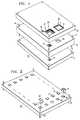
- the inventionmay be embodied in a assembly such as module assembly 10 which consists of two circuit card substrates 11 and 13 sandwiching a frame 12.
- An array of cross-over cell cavities 16 seen in FIG. 5are formed through frame 12.
- the cavities 16are shown uniformly arrayed, but may be placed in any convenient fashion.
- frame 12 with its cavities 16is to form the cavities out of hollow open-ended square blocks, such as block 9 seen in FIG. 5, which fit into square openings provided in top and bottom plates of the frame 12 (plates not shown).
- the remainder of the interior space between the top and bottom platesmay be provided with any desired shape to accommodate cooling fluid which, for example, may enter the assembly at coolant inlet 25 and exit at coolant outlet 26.
- the coolantmay be gaseous, such as forced air or alternatively liquid such as ordinary brake fluid.
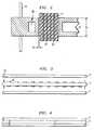
- slugs of elastomeric one-directional conductive material 17are placed in the cavities 16. If the cavities are square in cross-section as in the instant embodiment, the slugs are substantially square in cross-section also. It is advantageous to shape the slugs so that each has a somewhat lesser cross-sectional area than that of the cavity as suggested by the dimension denoted 8 in FIG. 2. At the same time, the height of each slug 17 is made to be greater that the depth or top-to-bottom dimension of the cavity 16 denoted 24 in FIG. 2. In a preferred embodiment of the invention, the volume of the slugs 17, when compressed in the manner to be described, will approximate the volume of the cavity 16 and preferably will at least equal it.
- the substrates 11 and 13include alignment holes 15 at each corner, which as seen also in FIGS. 3 and 4, mate with the four alignment pins 14 of frame 12. The alignment achieved is to assure that the cross-over cell pad arrays 18 appearing on the top surface of substrate 11 and the corresponding crossover cell pad arrays shown in dotted lines on the bottom of substrate 13 are in close vertical register.
- FIG. 1shows an array of chip cavities 19 formed on the surface of substrate 13. Similar cavities (not shown) are formed in the substrate 11, the latter being symmetrically located with respect to the cavities 19 of substrate 11.
- the chip cavities 19are a conventional way for containing in a frame such as frame 14, a multiplicity of semiconductor integrated circuits such as a multichip module 22.
- the cavities 19have a conventional bonding ledge 16 inset within the cavity on all four sides of which bonding ledge pads 20 appear.
- Wire bond connections such as wire 7 in FIG. 1are conventionally effected from the multichip module 7 to the pads 20.
- the pads 20, seen in FIG. 1,are connected by layered routing paths (not shown) within the interior of the substrates 11 and 13 in substantially any pattern or routing that is necessary to achieve the design of the computer architecture.
- the expedient of interior routingis well-known in the art; but while it does not form part of this invention, the invention greatly adds to the utility of the internal routing layers.
- connections from the pads 20 in each of the chip cavities 19 following internal routingeventually make appearances in cross-over cell pad arrays such as arrays 18 disposed on the interior surfaces of substrates 11 and 13.
- the slug 17contains a series of vertical conductive paths denoted 23.
- Slugs of elastomeric material with vertical or one-directional paths that are usable in this inventionmay be formed by any of several methods of fabrication. For example, .010 mil thick elastomer sheets with closely spaced gold conductive paths silk-screened on one side thereof may be adherently stacked and slugs of the desired length and cross-section then cut from the stack.
- the cross-section of the vertically conductive paths 23 of the slugs 17should be substantially less than the spacing between adjacent contact pads of the pad arrays 18 in order to prevent the shorting out of adjacent pads.
- the conductor-to-conductor spacing of the paths 23should be appropriately dense to assure a maximum of electrically conductive paths between corresponding contact elements of the oppositely disposed cross-over cell pad arrays 18.
- the components of the assembly 10are positioned as in FIG. 3 and then brought together by sliding the alignment holes 15 of the substrates 11 and 13 onto the alignment pins 14. In the assembled position, shown in FIG. 4, the slugs are compressed to substantially fill the cavities 16 with their compressed volume. For permanent sealing, the assembly may be bonded.
- FIG. 6graphs roughly the behavior of one elastomeric vertically conductive material that may be used in the present invention.
- Elastomeric connectorsmay, for example, be realized by starting with an array of metal strips running linearly through a silicone rubber body typically .0005" thick and .002" wide arranged in rows approximately .004", which then are laminated together to form a bulk of directionally conductive material. Silicone formulations have the advantage of flexibility at temperatures below -65 degrees C, yet are tolerant of elevated temperatures up to +175 degrees C. Further, silicones are unaffected by aging and typically do not become sticky, brittle or cracked.
- Siliconesshow little or no degradation when exposed to ultra-violet radiation, oxygen, ozone or humidity.
- One suitable elastomeric materialis available under the tradename "Matrix MOE” from Elastomeric Technologies, Inc. of Hatsboro, PA. Its behavior is depicted in FIG. 6. It is seen that as this material is compressed, its conductivity increases up to a point. An optimum range of maximum conductivity can be identified as a function of the pounds of applied compressive force in pounds per square inch occurring within a certain range. Thereafter, the conductivity decreases.
- FIG. 7shows the invention being used in a conventional circuit board or card enclosure 29.
- the backplane 30 of the enclosure 29contains the usual array of pin connectors 32.
- Rails 31mount one or more (usually many) assemblies 10.
- the female gang connectors 33which serve in conventional fashion as circuit paths to the outside world for each assembly 10 mate with pin connectors 32.
Landscapes
- Combinations Of Printed Boards (AREA)
- Multi-Conductor Connections (AREA)
- Coupling Device And Connection With Printed Circuit (AREA)
- Mounting Of Printed Circuit Boards And The Like (AREA)
Abstract
Description
- This invention relates to cross-over connections between circuit boards and particularly to effecting very short, high-density electrical connections in assemblies of such boards without having to use the front or exposed surfaces of the boards.
- The government has rights in this invention pursuant to Contract No. F33615-89-C-1036 awarded by the United States Air Force.
- Circuit boards embodying complex computer architectures frequently are stacked or paired. Such boards typically mount "chips" which may, for example, be processors or memory stores. Frequently, several chips are mounted in a planar gang on a miltichip module. As the computing and storage capacities of these equipments grow to meet new demands of speed and computing power, there is a need to package the chip boards more effectively and to realize more effective communications paths between adjacent boards.
- The traditional way to make connections or "cross-overs" between adjacent boards is to bring the internal circuits out to a pad array along the edge of the board, and then to connect the perimeter pads. An example of such a connection scheme is described in the patent application of Y. Lee-J. M. Segelken 1-6, Serial No. 07/387,480, filed 7/28/90, assigned to Applicant's assignee. That teaching relies on elastomeric one-directional conductive material to effect board-to-board connections.
- Many modern computers use modular card structures consisting of structural frames sandwiched between two circuit cards. The frame also contains ducts or paths for cooling the assembly. Communications interconnections between the cards typically are made via cross-over cables located in the card-edge connector or at the top edge of the card.
- This approach, however, places limitations on the number of cross-over paths that can be provided. These cross-over paths require that large amounts of board real estate be dedicated to cross-over pads and solder attachments. There also is a high risk of damage or contamination to the exposed cross-overs, which even delicate and careful handling does not always eliminate.
- The prior art cross-over cables also require substantial wiring lengths of, for example, three inches or more which significantly limits the speeds at which the computer may operate. An even further problem of the prior art design relates to crosstalk between crossover paths.
- Also, the successful use of directional conducting elastomers requires careful attention to containing the material and maintaining it in a relatively controlled compression. Prior art cross-over designs using elastomeric one-directional conductive material have experienced unacceptable variability of performance.
- Accordingly, one object of the invention is to provide a more reliable interconnection between adjacent chip-mounting circuit boards.
- Another object of the invention is to improve the speed of operation of stacked arrays of chip-containing circuit boards.
- A further object of the invention is to facilitate and simplify the assembly of such board arrays.
- A still further object of the invention is to make more reliable use of elastomeric one-directional conductive material to effect board-to-board connections.
- Another object of the invention is to realize a more dense packaging of computer components, particularly processors and memory chips.
- This invention is a highly efficient mechanism for achieving cross-over paths through a structural frame, using elastomeric one-dimensional conductive material. According to the invention, two chip-mounting substrates or boards are mounted on opposite sides of a structural frame. On the exterior side of each substrate are mounted one or more chips or discrete clusters of chips. One or more (usually several) discrete and separate areas on the interior side of each substrate are dedicated for the mounting of arrays of contact pads. These pads connect by various paths through and within the substrate to leads of the chips or chip arrays on the exterior side of the substrate. The frame includes interior passages through which either a gaseous or a liquid cooling fluid is conducted.
- In accordance with the invention, the frame is provided with an array of cross-over cell cavities which for example may be substantially square in cross-section. Each cavity is aligned with a corresponding cross-over cell pad array on the adjacent substrate. Slugs of elastomeric one-directional conductive material are placed in each cavity. Advantageously, each cavity is nominally of substantially the same volume as an uncompressed slug. Thus, for example, each slug may be formed with a somewhat lesser cross-sectional area than the cavity cross-section, but with a somewhat greater height than the thickness of the frame to provide an appropriate initial slug volume.
- Guide means are provided to align each substrate on respective sides of the frame so that the contact pad areas are facing each other and the intervening elastomer slug. Means also are provided for holding the two substrates together to compress the elastomeric material a predetermined amount while at the same time fastening the assembly. The elastomeric material thus compressed expands to fill and firmly lodge in its support chamber. The result is an assembly of two (or more) multi-chip module boards with internal cross-over cells which are sealed from contaminant and stabilized in their electrical conductivity by the close control over compressive forces and internal temperature made possible by the invention.
- FIG. 1 is an exploded perspective view of an assembly of the invention;
- FIG. 2 is partial sectional side view of the frame portion;
- FIG. 3 is an exploded side schematic view of the assembly;
- FIG. 4 is a side view of the assembly;
- FIG. 5 is a top perspective schematic view of the frame portion;
- FIG. 6 is a graph showing electrical performance of the elastomeric one-directional conductive material according to the invention; and
- FIG. 7 is a side perspective diagram of a circuit board or card enclosure for housing the assemblies.
- Referring to FIG. 1, the invention may be embodied in a assembly such as
module assembly 10 which consists of twocircuit card substrates frame 12. An array ofcross-over cell cavities 16 seen in FIG. 5 are formed throughframe 12. Thecavities 16 are shown uniformly arrayed, but may be placed in any convenient fashion. - One way to construct
frame 12 with itscavities 16 is to form the cavities out of hollow open-ended square blocks, such as block 9 seen in FIG. 5, which fit into square openings provided in top and bottom plates of the frame 12 (plates not shown). The remainder of the interior space between the top and bottom plates may be provided with any desired shape to accommodate cooling fluid which, for example, may enter the assembly atcoolant inlet 25 and exit atcoolant outlet 26. The coolant may be gaseous, such as forced air or alternatively liquid such as ordinary brake fluid. - In accordance with the invention, slugs of elastomeric one-directional
conductive material 17 are placed in thecavities 16. If the cavities are square in cross-section as in the instant embodiment, the slugs are substantially square in cross-section also. It is advantageous to shape the slugs so that each has a somewhat lesser cross-sectional area than that of the cavity as suggested by the dimension denoted 8 in FIG. 2. At the same time, the height of eachslug 17 is made to be greater that the depth or top-to-bottom dimension of thecavity 16 denoted 24 in FIG. 2. In a preferred embodiment of the invention, the volume of theslugs 17, when compressed in the manner to be described, will approximate the volume of thecavity 16 and preferably will at least equal it. - The
substrates alignment pins 14 offrame 12. The alignment achieved is to assure that the cross-overcell pad arrays 18 appearing on the top surface ofsubstrate 11 and the corresponding crossover cell pad arrays shown in dotted lines on the bottom ofsubstrate 13 are in close vertical register. - FIG. 1 shows an array of
chip cavities 19 formed on the surface ofsubstrate 13. Similar cavities (not shown) are formed in thesubstrate 11, the latter being symmetrically located with respect to thecavities 19 ofsubstrate 11. The chip cavities 19 are a conventional way for containing in a frame such asframe 14, a multiplicity of semiconductor integrated circuits such as amultichip module 22. Thecavities 19 have aconventional bonding ledge 16 inset within the cavity on all four sides of whichbonding ledge pads 20 appear. Wire bond connections such aswire 7 in FIG. 1 are conventionally effected from themultichip module 7 to thepads 20. - The
pads 20, seen in FIG. 1, are connected by layered routing paths (not shown) within the interior of thesubstrates - The connections from the
pads 20 in each of thechip cavities 19 following internal routing eventually make appearances in cross-over cell pad arrays such asarrays 18 disposed on the interior surfaces ofsubstrates - Returning to FIG. 2, it is seen that the
slug 17 contains a series of vertical conductive paths denoted 23. Slugs of elastomeric material with vertical or one-directional paths that are usable in this invention may be formed by any of several methods of fabrication. For example, .010 mil thick elastomer sheets with closely spaced gold conductive paths silk-screened on one side thereof may be adherently stacked and slugs of the desired length and cross-section then cut from the stack. - It will be appreciated that the cross-section of the vertically
conductive paths 23 of theslugs 17 should be substantially less than the spacing between adjacent contact pads of thepad arrays 18 in order to prevent the shorting out of adjacent pads. Within this limitation, the conductor-to-conductor spacing of thepaths 23 should be appropriately dense to assure a maximum of electrically conductive paths between corresponding contact elements of the oppositely disposed cross-overcell pad arrays 18. - With the
several modules 23 solder-connected to thebonding ledge pads 20, and the appropriatelysized slugs 17 placed in theirrespective cell cavities 16, the components of theassembly 10 are positioned as in FIG. 3 and then brought together by sliding the alignment holes 15 of thesubstrates cavities 16 with their compressed volume. For permanent sealing, the assembly may be bonded. - Desirably, the compression results in a firm frictional fit such as will hold the slugs in a permanent and stable position in their cavities. FIG. 6 graphs roughly the behavior of one elastomeric vertically conductive material that may be used in the present invention. Elastomeric connectors may, for example, be realized by starting with an array of metal strips running linearly through a silicone rubber body typically .0005" thick and .002" wide arranged in rows approximately .004", which then are laminated together to form a bulk of directionally conductive material. Silicone formulations have the advantage of flexibility at temperatures below -65 degrees C, yet are tolerant of elevated temperatures up to +175 degrees C. Further, silicones are unaffected by aging and typically do not become sticky, brittle or cracked. Silicones show little or no degradation when exposed to ultra-violet radiation, oxygen, ozone or humidity. One suitable elastomeric material is available under the tradename "Matrix MOE" from Elastomeric Technologies, Inc. of Hatsboro, PA. Its behavior is depicted in FIG. 6. It is seen that as this material is compressed, its conductivity increases up to a point. An optimum range of maximum conductivity can be identified as a function of the pounds of applied compressive force in pounds per square inch occurring within a certain range. Thereafter, the conductivity decreases. It is necessary, therefore, to identify the conductivity variability of the elastomeric vertically conductive material with compression and, based on that assessment, select the volume of each slug such that as it compresses to substantially fill the receiving cavity the conductivity falls within the desired maximum range. The appealing aspect of the instant invention is that the material cannot be over-compressed provided the arithmetic of the volume calculation has been performed properly.
- FIG. 7 shows the invention being used in a conventional circuit board or
card enclosure 29. Thebackplane 30 of theenclosure 29 contains the usual array ofpin connectors 32.Rails 31 mount one or more (usually many)assemblies 10. Thefemale gang connectors 33 which serve in conventional fashion as circuit paths to the outside world for eachassembly 10 mate withpin connectors 32.
Claims (10)
- A circuit board assembly CHARACTERIZED BY:
first and second circuit board substrates each CHARACTERIZED BY one or more exterior-mounted chip modules each chip having connections to symmetrically located discrete pad clusters disposed on the interior side of said substrates; and
cross-over connections between the corresponding said pad clusters, CHARACTERIZED BY:
a two-sided frame for receiving on opposite sides thereof said respective substrates;
cross-over cell cavities through said frame and aligned with said corresponding pad clusters; and
an elastomeric one-directional conductive material slug disposed in each said cell cavity, the volume of each slug when compressed approximating the volume of said cell cavity. - Apparatus in accordance with claim 1, wherein said substrates further comprise two or more alignment holes at the substrate corners, and wherein said frame further comprises alignment pins for engaging said alignment holes, thereby to assure that said cross-over cell pad arrays appearing on the top surface of said first substrate and the corresponding cross-over cell pad arrays on the bottom surface of said second substrate are in close vertical register.
- Apparatus in accordance with claim 2, wherein each said slug comprises a plurality of vertical conductive paths the ends thereof terminating at the exterior opposite vertical surfaces of each slug to make electrical contact with the pads of said pad clusters.
- Apparatus in accordance with claim 3, wherein the cross-section of the vertically conductive paths of said slugs is substantially less than the lateral spacing between adjacent contact pads of said pad arrays.
- Apparatus in accordance with claim 4, wherein said slug-receiving cavities are formed from hollow open-ended square blocks.
- Apparatus in accordance with claim 5, further CHARACTERIZED BY bonding means to adhere said frame to said first and second substrates.
- Apparatus in accordance with claim 6, wherein said elastomeric slugs are compressed to a degree which places the resulting slug conductivity within substantially the maximum conductivity range of which the material is capable.
- Apparatus in accordance with claim 7, wherein the interior of said frame is hollow, said apparatus further CHARACTERIZED BY means for flowing coolant into and out of said interior.
- Apparatus in accordance with claim 8, wherein the volume of each slug when compressed substantially equals the volume of said slug-receiving cavity.
- Apparatus in accordance with claims 1, 2, 3, 4, 5, 6, 7, 8, and 9, further CHARACTERIZED BY enclosure means for housing one or more said assemblies, said means CHARACTERIZED BY a backplane including a pin array, dual rail means slidably mounting individual said assemblies and female gang connectors connecting said assembly to said pin array when said assembly is positioned on said slides onto said backplane.
Applications Claiming Priority (2)
| Application Number | Priority Date | Filing Date | Title |
|---|---|---|---|
| US84409992A | 1992-03-02 | 1992-03-02 | |
| US844099 | 1992-03-02 |
Publications (2)
| Publication Number | Publication Date |
|---|---|
| EP0558855A2true EP0558855A2 (en) | 1993-09-08 |
| EP0558855A3 EP0558855A3 (en) | 1996-05-01 |
Family
ID=25291818
Family Applications (1)
| Application Number | Title | Priority Date | Filing Date |
|---|---|---|---|
| EP92311248AWithdrawnEP0558855A3 (en) | 1992-03-02 | 1992-12-10 | Circuit board stack with novel cross-over cells |
Country Status (2)
| Country | Link |
|---|---|
| EP (1) | EP0558855A3 (en) |
| JP (1) | JP2598212B2 (en) |
Cited By (13)
| Publication number | Priority date | Publication date | Assignee | Title |
|---|---|---|---|---|
| US5657206A (en)* | 1994-06-23 | 1997-08-12 | Cubic Memory, Inc. | Conductive epoxy flip-chip package and method |
| US5661087A (en)* | 1994-06-23 | 1997-08-26 | Cubic Memory, Inc. | Vertical interconnect process for silicon segments |
| US5675397A (en)* | 1994-06-09 | 1997-10-07 | Nec Corporation | Electric connecting structure of display equipment |
| US5698895A (en)* | 1994-06-23 | 1997-12-16 | Cubic Memory, Inc. | Silicon segment programming method and apparatus |
| EP0889678A1 (en)* | 1997-07-04 | 1999-01-07 | Hewlett-Packard Company | Compressible elastomeric contact and mechanical assembly therewith |
| US5891761A (en)* | 1994-06-23 | 1999-04-06 | Cubic Memory, Inc. | Method for forming vertical interconnect process for silicon segments with thermally conductive epoxy preform |
| US6080596A (en)* | 1994-06-23 | 2000-06-27 | Cubic Memory Inc. | Method for forming vertical interconnect process for silicon segments with dielectric isolation |
| US6124633A (en)* | 1994-06-23 | 2000-09-26 | Cubic Memory | Vertical interconnect process for silicon segments with thermally conductive epoxy preform |
| US6255726B1 (en) | 1994-06-23 | 2001-07-03 | Cubic Memory, Inc. | Vertical interconnect process for silicon segments with dielectric isolation |
| WO2002065588A1 (en)* | 2001-02-09 | 2002-08-22 | Jsr Corporation | Anisotropic conductive connector, its manufacture method and probe member |
| US6486528B1 (en) | 1994-06-23 | 2002-11-26 | Vertical Circuits, Inc. | Silicon segment programming apparatus and three terminal fuse configuration |
| US7286365B2 (en)* | 2002-10-11 | 2007-10-23 | Thales | Electronic substrate for a three-dimensional electronic module |
| CN113178421A (en)* | 2021-04-08 | 2021-07-27 | 深圳市磐锋精密技术有限公司 | Multi-chip packaging positioning device and method for mobile phone integrated circuit |
Family Cites Families (9)
| Publication number | Priority date | Publication date | Assignee | Title |
|---|---|---|---|---|
| US4209481A (en)* | 1976-04-19 | 1980-06-24 | Toray Industries, Inc. | Process for producing an anisotropically electroconductive sheet |
| JPS54158691A (en)* | 1977-10-21 | 1979-12-14 | Univ Melbourne | Electrical connector |
| FR2538989B1 (en)* | 1982-12-30 | 1985-10-04 | Thomson Csf | ASSEMBLY STRUCTURE FOR COMPLEX ELECTRONIC CIRCUITS, AND METHOD FOR IMPROVING THE RELIABILITY OF SUCH AN ASSEMBLY |
| GB8405598D0 (en)* | 1984-03-02 | 1984-04-04 | Plessey Co Plc | Electrical connectors |
| US4593961A (en)* | 1984-12-20 | 1986-06-10 | Amp Incorporated | Electrical compression connector |
| US4988306A (en)* | 1989-05-16 | 1991-01-29 | Labinal Components And Systems, Inc. | Low-loss electrical interconnects |
| JPH0494072A (en)* | 1990-08-10 | 1992-03-26 | Matsushita Electric Ind Co Ltd | Connector for printed substrate |
| US5030109A (en)* | 1990-08-24 | 1991-07-09 | Amp Incorporated | Area array connector for substrates |
| US5037312A (en)* | 1990-11-15 | 1991-08-06 | Amp Incorporated | Conductive gel area array connector |
- 1992
- 1992-12-10EPEP92311248Apatent/EP0558855A3/ennot_activeWithdrawn
- 1992-12-28JPJP4358564Apatent/JP2598212B2/ennot_activeExpired - Fee Related
Cited By (22)
| Publication number | Priority date | Publication date | Assignee | Title |
|---|---|---|---|---|
| US5675397A (en)* | 1994-06-09 | 1997-10-07 | Nec Corporation | Electric connecting structure of display equipment |
| GB2290159B (en)* | 1994-06-09 | 1998-07-08 | Nec Corp | Electric connecting structure of display equipment |
| US6080596A (en)* | 1994-06-23 | 2000-06-27 | Cubic Memory Inc. | Method for forming vertical interconnect process for silicon segments with dielectric isolation |
| US6255726B1 (en) | 1994-06-23 | 2001-07-03 | Cubic Memory, Inc. | Vertical interconnect process for silicon segments with dielectric isolation |
| US5698895A (en)* | 1994-06-23 | 1997-12-16 | Cubic Memory, Inc. | Silicon segment programming method and apparatus |
| US5661087A (en)* | 1994-06-23 | 1997-08-26 | Cubic Memory, Inc. | Vertical interconnect process for silicon segments |
| US5837566A (en)* | 1994-06-23 | 1998-11-17 | Cubic Memory, Inc. | Vertical interconnect process for silicon segments |
| US5675180A (en)* | 1994-06-23 | 1997-10-07 | Cubic Memory, Inc. | Vertical interconnect process for silicon segments |
| US5891761A (en)* | 1994-06-23 | 1999-04-06 | Cubic Memory, Inc. | Method for forming vertical interconnect process for silicon segments with thermally conductive epoxy preform |
| US5994170A (en) | 1994-06-23 | 1999-11-30 | Cubic Memory, Inc. | Silicon segment programming method |
| US5657206A (en)* | 1994-06-23 | 1997-08-12 | Cubic Memory, Inc. | Conductive epoxy flip-chip package and method |
| US6124633A (en)* | 1994-06-23 | 2000-09-26 | Cubic Memory | Vertical interconnect process for silicon segments with thermally conductive epoxy preform |
| US6486528B1 (en) | 1994-06-23 | 2002-11-26 | Vertical Circuits, Inc. | Silicon segment programming apparatus and three terminal fuse configuration |
| US6188126B1 (en) | 1994-06-23 | 2001-02-13 | Cubic Memory Inc. | Vertical interconnect process for silicon segments |
| EP0889678A1 (en)* | 1997-07-04 | 1999-01-07 | Hewlett-Packard Company | Compressible elastomeric contact and mechanical assembly therewith |
| US6183272B1 (en) | 1997-07-04 | 2001-02-06 | Hewlett-Packard Company | Compressible elastomeric contact and mechanical assembly therewith |
| WO2002065588A1 (en)* | 2001-02-09 | 2002-08-22 | Jsr Corporation | Anisotropic conductive connector, its manufacture method and probe member |
| US6969622B1 (en) | 2001-02-09 | 2005-11-29 | Jsr Corporation | Anisotropically conductive connector, its manufacture method and probe member |
| US7323712B2 (en) | 2001-02-09 | 2008-01-29 | Jsr Corporation | Anisotropically conductive connector and production process thereof, and probe member |
| US7286365B2 (en)* | 2002-10-11 | 2007-10-23 | Thales | Electronic substrate for a three-dimensional electronic module |
| CN113178421A (en)* | 2021-04-08 | 2021-07-27 | 深圳市磐锋精密技术有限公司 | Multi-chip packaging positioning device and method for mobile phone integrated circuit |
| CN113178421B (en)* | 2021-04-08 | 2022-03-29 | 深圳市磐锋精密技术有限公司 | Multi-chip packaging positioning device and method for mobile phone integrated circuit |
Also Published As
| Publication number | Publication date |
|---|---|
| JPH0684570A (en) | 1994-03-25 |
| EP0558855A3 (en) | 1996-05-01 |
| JP2598212B2 (en) | 1997-04-09 |
Similar Documents
| Publication | Publication Date | Title |
|---|---|---|
| US5025306A (en) | Assembly of semiconductor chips | |
| US5140405A (en) | Semiconductor assembly utilizing elastomeric single axis conductive interconnect | |
| US4283754A (en) | Cooling system for multiwafer high density circuit | |
| US6014313A (en) | Packaging structure for integrated circuits | |
| US4841355A (en) | Three-dimensional microelectronic package for semiconductor chips | |
| US5208729A (en) | Multi-chip module | |
| US5604377A (en) | Semiconductor chip high density packaging | |
| US5224023A (en) | Foldable electronic assembly module | |
| US5014161A (en) | System for detachably mounting semiconductors on conductor substrate | |
| US3812402A (en) | High density digital systems and their method of fabrication with liquid cooling for semi-conductor circuit chips | |
| EP0558855A2 (en) | Circuit board stack with novel cross-over cells | |
| US5007841A (en) | Integrated-circuit chip interconnection system | |
| US3648113A (en) | Electronic assembly having cooling means for stacked modules | |
| EP1264347B1 (en) | Electronic module having a three dimensional array of carrier-mounted integrated circuit packages | |
| US5218515A (en) | Microchannel cooling of face down bonded chips | |
| US4581679A (en) | Multi-element circuit construction | |
| US5943213A (en) | Three-dimensional electronic module | |
| US3706010A (en) | Packaging structure having cooling means for a multiplicity of hermetic modules for integrated circuit chips | |
| US5227995A (en) | High density semiconductor memory module using split finger lead frame | |
| WO1993018547A1 (en) | Three dimensional, multi-chip module | |
| TW202234970A (en) | Electronic assembly including a compression assembly for cable connector modules | |
| JPH0513661A (en) | Three-dimensional circuit module and its structure | |
| KR20030071763A (en) | Electronic module having canopy-type carriers | |
| US6540525B1 (en) | High I/O stacked modules for integrated circuits | |
| EP0245179B1 (en) | System for detachably mounting semiconductors on conductor substrate. |
Legal Events
| Date | Code | Title | Description |
|---|---|---|---|
| PUAI | Public reference made under article 153(3) epc to a published international application that has entered the european phase | Free format text:ORIGINAL CODE: 0009012 | |
| AK | Designated contracting states | Kind code of ref document:A2 Designated state(s):DE FR GB NL | |
| RAP3 | Party data changed (applicant data changed or rights of an application transferred) | Owner name:AT&T CORP. | |
| PUAL | Search report despatched | Free format text:ORIGINAL CODE: 0009013 | |
| AK | Designated contracting states | Kind code of ref document:A3 Designated state(s):DE FR GB NL | |
| 17P | Request for examination filed | Effective date:19961018 | |
| 17Q | First examination report despatched | Effective date:19981125 | |
| 18D | Application deemed to be withdrawn | Effective date:19990607 |