EP0549377A2 - A scrubber apparatus for cleaning a thin disk work - Google Patents
A scrubber apparatus for cleaning a thin disk workDownload PDFInfo
- Publication number
- EP0549377A2 EP0549377A2EP92311839AEP92311839AEP0549377A2EP 0549377 A2EP0549377 A2EP 0549377A2EP 92311839 AEP92311839 AEP 92311839AEP 92311839 AEP92311839 AEP 92311839AEP 0549377 A2EP0549377 A2EP 0549377A2
- Authority
- EP
- European Patent Office
- Prior art keywords
- wafer
- work
- rotatory
- rotatory plate
- suction head
- Prior art date
- Legal status (The legal status is an assumption and is not a legal conclusion. Google has not performed a legal analysis and makes no representation as to the accuracy of the status listed.)
- Granted
Links
- 238000004140cleaningMethods0.000titleclaimsabstractdescription18
- 230000001680brushing effectEffects0.000claimsabstractdescription20
- 230000002093peripheral effectEffects0.000claimsabstractdescription12
- 239000004065semiconductorSubstances0.000abstractdescription7
- 235000012431wafersNutrition0.000description44
- 239000002002slurrySubstances0.000description10
- 238000005498polishingMethods0.000description7
- 238000010276constructionMethods0.000description3
- 230000008878couplingEffects0.000description2
- 238000010168coupling processMethods0.000description2
- 238000005859coupling reactionMethods0.000description2
- 238000000034methodMethods0.000description2
- 238000005201scrubbingMethods0.000description2
- XLYOFNOQVPJJNP-UHFFFAOYSA-NwaterSubstancesOXLYOFNOQVPJJNP-UHFFFAOYSA-N0.000description2
- 239000013078crystalSubstances0.000description1
- 230000000694effectsEffects0.000description1
- 239000007788liquidSubstances0.000description1
- 238000012986modificationMethods0.000description1
- 230000004048modificationEffects0.000description1
- 239000002245particleSubstances0.000description1
- 229910052710siliconInorganic materials0.000description1
- 239000010703siliconSubstances0.000description1
- 239000007787solidSubstances0.000description1
- 239000000758substrateSubstances0.000description1
- 238000007669thermal treatmentMethods0.000description1
- 238000011282treatmentMethods0.000description1
Images


Classifications
- H—ELECTRICITY
- H01—ELECTRIC ELEMENTS
- H01L—SEMICONDUCTOR DEVICES NOT COVERED BY CLASS H10
- H01L21/00—Processes or apparatus adapted for the manufacture or treatment of semiconductor or solid state devices or of parts thereof
- H01L21/67—Apparatus specially adapted for handling semiconductor or electric solid state devices during manufacture or treatment thereof; Apparatus specially adapted for handling wafers during manufacture or treatment of semiconductor or electric solid state devices or components ; Apparatus not specifically provided for elsewhere
- H01L21/67005—Apparatus not specifically provided for elsewhere
- H01L21/67011—Apparatus for manufacture or treatment
- H01L21/67017—Apparatus for fluid treatment
- H01L21/67028—Apparatus for fluid treatment for cleaning followed by drying, rinsing, stripping, blasting or the like
- B—PERFORMING OPERATIONS; TRANSPORTING
- B08—CLEANING
- B08B—CLEANING IN GENERAL; PREVENTION OF FOULING IN GENERAL
- B08B1/00—Cleaning by methods involving the use of tools
- B08B1/30—Cleaning by methods involving the use of tools by movement of cleaning members over a surface
- B08B1/32—Cleaning by methods involving the use of tools by movement of cleaning members over a surface using rotary cleaning members
- B08B1/36—Cleaning by methods involving the use of tools by movement of cleaning members over a surface using rotary cleaning members rotating about an axis orthogonal to the surface
Definitions
- the present inventionrelates to a scrubber cleaning apparatus for cleaning a thin disk work, such as semiconductor wafers; more particularly the invention relates to a scrubber apparatus for holding a thin disk work by sucking at one of the faces thereof by means of a sucking means and cleaning the circumferential periphery as well as that face of the work which is not being sucked (hereinafter "unsucked face").
- a semiconductor waferwhich is used to make substrates for semiconductor devices, is obtained from a single crystal ingot, such as one grown of molten polycrystal silicon, by slicing the ingot into thin disks orthogonally to the axis of the ingot, which disks are then chambered, lapped, etched, annealed, polished, and given other finishing treatments.
- the entire edges of the semiconductor waferare chamfered so as to fashion the wafer edges difficult to chip; however, the current tendency is to polish the chamfers and make them glossy (specular finish polishing) so as to nullify the possibility of creation of particles due to microscopic chipping and to prevent slippage of the wafer during thermal treatment.
- slurrypolishing liquid
- the wafermay be locally etched and such surface is liable to be damaged.
- the slurry sticking to the waferought to be removed as quickly as possible.
- the present inventionwas contrived in view of these problems, and it is, therefore, an object of the invention to provide a cleaning apparatus which can scrub one face of a thin disk work and the edges thereof;at the same time and thus clean them effectively.
- a new scrubber cleaning apparatusfor cleaning a thin disk work, comprising: a work holder means capable of holding the work by vacuum suction and turning the work circumferentially, and including a work suction head for fixing a work on it and a drive means to rotate said suction head; and a brush means including: a rotatory plate having a brushing surface on one side thereof, the brushing surface consisting of a flat ring portion and a side-of-cylinder portion, and being capable of shifting axially and in radial directions; a drive means for rotating said rotatory plate; a drive means for shifting said rotatory plate axially; and a drive means for shifting said rotatory plate in radial directions, said side-of-cylinder portion of said brushing surface being axially extending from the inner boundary of said ring portion, and said rotatory plate being disposed such that said flat ring portion of the brushing surface of the brush means is opposed to and in parallel to the unsucked face of the work which is held on the
- the suction headis turned in the same direction as the rotatory plate of the brush means, so that the side-of-cylinder portion runs counter to the peripheral chamfers of the work.
- the thin workis sucked by the work suction head and turned, and meanwhile the rotatory plate of the brush means is also turned and shifted axially so that the flat ring portion of the brushing (scrubbing) surface is first pressed on the unsucked face of the wafer, and thereafter the rotatory plate is moved sideways so that the side-of-cylinder portion is pressed on the peripheral chamfers of the wafer; consequently, the unsucked face of the wafer is scrubbed by the flat ring portion of the brushing surface and, almost at the same time, the peripheral chamfers of the which are scrubbed by the side-of-cylinder portion of the brushing surface. Since it is so arranged that the side-of-cylinder portion runs counter to the peripheral chamfers of the wafer, the chamfers are thoroughly cleaned, let alone the unsucked face of the wafer.
- Fig. 1is a horizontal cross section of a scrubber cleaning apparatus according to the present invention
- Fig. 2is a view of the same cleaning apparatus of Fig. 1 seen in the direction indicated by the arrow A
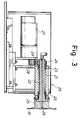
- Fig. 3is a vertical cross section of a work suction rotary assembly
- Fig. 4 and Fig. 5are, respectively, a side view and a front view of a rotatory brush to show the position of the wafer in relation to the rotatory brush.
- the reference numeral 1designates a casing, and a holder 2 is horizontally fixed at an upper part inside the casing 1, and a ball bush 3 is set inside the holder 2.
- a horizontal duplex constructionconsisting of a hollow shaft 4 and a solid rotatory shaft 5 inserted therein, is inserted in the holder 2 in a manner such that the duplex construction is capable of freely sliding to and fro inside the holder 2 (right-ward and left-ward in Fig. 1).
- a case 6is fixedly connected at its one end to the free end of the hollow shaft 4 which extends out from the casing 1, and a pulley 7 is locked about that end of the rotatory shaft 5 which is disposed in the case 6.
- the rotatory shaft 5is supported in a manner such that it can freely rotate in the hollow shaft 4.
- a rotatory shaft 8is supported by the case 6 at the other end thereof in a manner such that the shaft 8 is parallel to the rotatory shaft 5 and is freely rotative, and a pulley 9 is locked about that end portion of the rotatory shaft 8 which is disposed in the case 8.
- a belt 10is passed round the pulley 9 and the pulley 7 to thereby correct them.
- a rotatory brush 11 having a shape of circular diskis locked about that end portion of the rotatory shaft 8 which extends out from the case 6, and this rotatory brush 11 consists of a flat portion 11a and an cylindrical protrusion portion 11b axially embossed from the middle of the flat portion 11a.
- the brushing surfaces of this rotatory brush 11consist of a flat ring portion and a side-of-cylinder portion (the side of the embossed cylinder 11b). Incidentally, these brushing surfaces are planted densely with hair such as plastic hair.
- An arm 12is locked about that end of the hollow shaft 4 which is disposed in the casing 1, and to the free end of the arm 12 is corrected pivotally a rod 13a of a cylinder 13, which is a drive means; the other end of the cylinder 13 is pivotally corrected to a bracket 14, which is fixed on the casing 1.
- a vertical plate 15is provided in the casing 1 and the hollow shaft 4 is supported by the plate 15 in a manner such that the shaft 4 can freely rotate on the plate 15.
- a drive motor 16 as the revolver means and a cylinder 17 as the shifter meansare fixed to the plate 15, and the output shaft 16a of the drive motor 16 is connected via a coupling 18 to that end of the rotatory shaft 5 which is inside the casing 1.
- the rod 17a extending from the cylinder 17is fixed in a bracket 19, which is bolted on the holder 2.
- a frame 21is horizontally fixed near the ceiling of the work holder assembly 20, and a rotatory shaft 22 is inserted in the frame 21 and borne horizontally by a set of bearing 23 in a manner such that the shaft 22 can rotate freely.
- a pulley 24is locked about one end of the rotatory shaft 22 (the end which is remote from the brush 11) and a suction head 25 is locked about the other end of the shaft 22 (the end which opposes the brush 11).
- a drive motor 27 of speed variable typeis fixed behind the rotatory shaft 22 inside the work holder assembly 20, and the output shaft of the motor 27 is disposed underneath the rear end of the shaft 22, and a belt 29 is passed round a pulley 28 locked about the output shaft of the drive motor 27 and the pulley 24 to thereby connect them.
- the descriptionwill concern the case where a semiconductor wafer W is cleaned whose peripheral chamfers have been polished with slurry to specular gloss.
- the vacuum pumpnot shown, is driven to draw the air from the vacuum passage bore 26, this semiconductor wafer W is sucked by the negative pressure created in the passage bore 26, and pressed on the face of the suction head 25 of the work holder assembly 20 and thus held vertically, as shown.
- the drive motor 27is driven and its rotation torque created is transmitted to the rotation shaft 22 via the pulley 28, belt 29 and pulley 24, whereupon the shaft 22 is caused to turn at a regular rotational speed together with the wafer W held at the suction head 25.
- the drive motor 16is driven and its rotational torque is transmitted to the rotatory shaft 8 via the output shaft 16a, coupling 18, rotatory shaft 5, pulley 7, belt 10 and pulley 9, whereupon the rotatory shaft 8 together with the rotatory brush 11 is caused to turn at a regular rotational speed.
- the air cylinder 17is driven such that the rod 17a is pushed out, whereby the cylinder 17, plate 15, drive motor 16, hollow shaft 4 and rotatory shaft 5 are altogether pushed back (left-ward as seen in Fig. 1), and the rotatory brush 11 interconnected to the hollow shaft 4 is also shifted and, as the result, the flat portion 11a of the rotatory brush 11 comes in contact with the unsucked face of the wafer W, as shown in Fig. 4.
- the air cylinder 13is operated such that its rod 13a is pushed out, the arm 12 and the hollow shaft 4 are turned about the axis of the shaft 4 clockwise, as seen in Fig. 2.
- the rotatory brush 11 supported integrally by the hollow shaft 4is swung a little from its position drawn in solid line, in fig. 2, to a lower position drawn in two-dot chain line.
- the rotatory brush 11is shifted along a circular locus, or, in other words, in continuously changing and always radial directions. Consequently, as shown in Fig. 5, the embossed portion 11b of the rotatory brush 11 is brought to ride on the peripheral edge of the wafer W.
- the wafer Wis turned in the same direction as the brush 11 and, as the result, the circumference of the turning embossed portion 11 runs in the opposite direction to the running edge of the wafer W in a manner such that they rub against each other.
- the unsucked face of the wafer Wis scrubbed by the flat portion 11a of the rotatory brush 11 and the peripheral chamfers of the same wafer W are scrubbed by the embossed portion 11b of the rotatory brush 11 so that both the unsucked face and the peripheral chamfers of the wafer W are effectively cleaned almost simultaneously in one course of scrubbing operation.
- the unsucked face and the peripheral chamfers of the wafer Ware scrubbed clean but the sucked face remains uncleaned; however, since the sucked face will be polished at the next polishing step, this is not a problem.
- a scrubber cleaning apparatuswhich in essence consists of: a work (wafer) holder means capable of holding a wafer by vacuum suction and turning the wafer circumferentially, and including a wafer suction head for fixing a wafer on it and a drive means to rotate said suction head; and a brush means including: a rotatory plate having a brushing surface on one side consisting of a flat ring portion and a side-of-cylinder portion, and being capable of shifting axially and in radial directions; a drive means for rotating said rotatory plate circumferentially; a drive means for shifting said rotatory plate axially; and a drive means for shifting said rotatory plate in radial directions, said side-of-cylinder portion of said brushing surface axially extending from the inner boundary of said ring portion, and furthermore, said rotatory plate being disposed such that said flat ring portion of the brushing surface of the brush means is opposed to and in
Landscapes
- Engineering & Computer Science (AREA)
- Physics & Mathematics (AREA)
- Condensed Matter Physics & Semiconductors (AREA)
- General Physics & Mathematics (AREA)
- Manufacturing & Machinery (AREA)
- Computer Hardware Design (AREA)
- Microelectronics & Electronic Packaging (AREA)
- Power Engineering (AREA)
- Cleaning Or Drying Semiconductors (AREA)
Abstract
Description
- The present invention relates to a scrubber cleaning apparatus for cleaning a thin disk work, such as semiconductor wafers; more particularly the invention relates to a scrubber apparatus for holding a thin disk work by sucking at one of the faces thereof by means of a sucking means and cleaning the circumferential periphery as well as that face of the work which is not being sucked (hereinafter "unsucked face").
- A semiconductor wafer, which is used to make substrates for semiconductor devices, is obtained from a single crystal ingot, such as one grown of molten polycrystal silicon, by slicing the ingot into thin disks orthogonally to the axis of the ingot, which disks are then chambered, lapped, etched, annealed, polished, and given other finishing treatments.
- As for the chamfering, the entire edges of the semiconductor wafer are chamfered so as to fashion the wafer edges difficult to chip; however, the current tendency is to polish the chamfers and make them glossy (specular finish polishing) so as to nullify the possibility of creation of particles due to microscopic chipping and to prevent slippage of the wafer during thermal treatment.
- In the polishing operation to make the wafer chamfers glossy, slurry (polishing liquid) is used. However, when the slurry remains on the wafer after the specular finish polishing, the wafer may be locally etched and such surface is liable to be damaged. Hence, the slurry sticking to the wafer ought to be removed as quickly as possible.
- Thus, methods have been adopted (i) wherein the wafer after specular finish polishing is dropped in water to wash the slurry off the wafer surface or (ii) wherein the wafer after specular finish polishing is held between a pair of rotatory brushes and the wafer is brushed to get rid of the slurry by turning the brushes and the wafer itself.
- However, it is impossible to entirely remove the sticking slurry by merely dropping the wafer in water. Also, in the case of the method of removing the slurry by brushing between the rotatory brushes, although it is possible to remove the slurry from the both faces of the wafer, it is not possible to effectively remove the slurry sticking on the chamfers made along the periphery of the wafer.
- The present invention was contrived in view of these problems, and it is, therefore, an object of the invention to provide a cleaning apparatus which can scrub one face of a thin disk work and the edges thereof;at the same time and thus clean them effectively.
- Herein is proposed, therefore, a new scrubber cleaning apparatus for cleaning a thin disk work, comprising:
a work holder means capable of holding the work by vacuum suction and turning the work circumferentially, and including a work suction head for fixing a work on it and a drive means to rotate said suction head; and
a brush means including: a rotatory plate having a brushing surface on one side thereof, the brushing surface consisting of a flat ring portion and a side-of-cylinder portion, and being capable of shifting axially and in radial directions; a drive means for rotating said rotatory plate; a drive means for shifting said rotatory plate axially; and a drive means for shifting said rotatory plate in radial directions,
said side-of-cylinder portion of said brushing surface being axially extending from the inner boundary of said ring portion, and
said rotatory plate being disposed such that said flat ring portion of the brushing surface of the brush means is opposed to and in parallel to the unsucked face of the work which is held on the suction head. - Preferably, the suction head is turned in the same direction as the rotatory plate of the brush means, so that the side-of-cylinder portion runs counter to the peripheral chamfers of the work.
- According to the invention, therefore, the thin work is sucked by the work suction head and turned, and meanwhile the rotatory plate of the brush means is also turned and shifted axially so that the flat ring portion of the brushing (scrubbing) surface is first pressed on the unsucked face of the wafer, and thereafter the rotatory plate is moved sideways so that the side-of-cylinder portion is pressed on the peripheral chamfers of the wafer; consequently, the unsucked face of the wafer is scrubbed by the flat ring portion of the brushing surface and, almost at the same time, the peripheral chamfers of the which are scrubbed by the side-of-cylinder portion of the brushing surface. Since it is so arranged that the side-of-cylinder portion runs counter to the peripheral chamfers of the wafer, the chamfers are thoroughly cleaned, let alone the unsucked face of the wafer.
- Fig. 1 is a horizontal cross section of a scrubber cleaning apparatus according to the present invention;
- Fig. 2 is a view of the same cleaning apparatus of Fig. 1 seen in the direction indicated by the arrow A;
- Fig. 3 is a vertical cross section of a work suction rotary assembly of the cleaning apparatus;
- Fig. 4 is a side view of a rotatory brush to show the position of the wafer in relation to the rotatory brush; and
- Fig. 5 is a front view of the rotatory brush so show the position of the wafer in relation to the rotatory brush.
- Next, an embodiment of the present invention, considered as the best mode, will be described with reference to the attached drawings.
- Fig. 1 is a horizontal cross section of a scrubber cleaning apparatus according to the present invention; Fig. 2 is a view of the same cleaning apparatus of Fig. 1 seen in the direction indicated by the arrow A; Fig. 3 is a vertical cross section of a work suction rotary assembly; and Fig. 4 and Fig. 5 are, respectively, a side view and a front view of a rotatory brush to show the position of the wafer in relation to the rotatory brush.
- In Fig. 1 and Fig. 2, the
reference numeral 1 designates a casing, and aholder 2 is horizontally fixed at an upper part inside thecasing 1, and aball bush 3 is set inside theholder 2. A horizontal duplex construction, consisting of a hollow shaft 4 and a solidrotatory shaft 5 inserted therein, is inserted in theholder 2 in a manner such that the duplex construction is capable of freely sliding to and fro inside the holder 2 (right-ward and left-ward in Fig. 1). - A
case 6 is fixedly connected at its one end to the free end of the hollow shaft 4 which extends out from thecasing 1, and apulley 7 is locked about that end of therotatory shaft 5 which is disposed in thecase 6. Incidentally, therotatory shaft 5 is supported in a manner such that it can freely rotate in the hollow shaft 4. - Also, a
rotatory shaft 8 is supported by thecase 6 at the other end thereof in a manner such that theshaft 8 is parallel to therotatory shaft 5 and is freely rotative, and apulley 9 is locked about that end portion of therotatory shaft 8 which is disposed in thecase 8. Abelt 10 is passed round thepulley 9 and thepulley 7 to thereby correct them. A rotatory brush 11 having a shape of circular disk is locked about that end portion of therotatory shaft 8 which extends out from thecase 6, and this rotatory brush 11 consists of aflat portion 11a and ancylindrical protrusion portion 11b axially embossed from the middle of theflat portion 11a. The brushing surfaces of this rotatory brush 11 consist of a flat ring portion and a side-of-cylinder portion (the side of the embossedcylinder 11b). Incidentally, these brushing surfaces are planted densely with hair such as plastic hair. - An
arm 12 is locked about that end of the hollow shaft 4 which is disposed in thecasing 1, and to the free end of thearm 12 is corrected pivotally arod 13a of acylinder 13, which is a drive means; the other end of thecylinder 13 is pivotally corrected to abracket 14, which is fixed on thecasing 1. - A
vertical plate 15 is provided in thecasing 1 and the hollow shaft 4 is supported by theplate 15 in a manner such that the shaft 4 can freely rotate on theplate 15. Adrive motor 16 as the revolver means and acylinder 17 as the shifter means are fixed to theplate 15, and theoutput shaft 16a of thedrive motor 16 is connected via acoupling 18 to that end of therotatory shaft 5 which is inside thecasing 1. Also, therod 17a extending from thecylinder 17 is fixed in abracket 19, which is bolted on theholder 2. - As shown in Fig. 1, an
assembly 20 having arotatory suction head 25 for holding and turning the work is annexed to the side of thecasing 1. Next, therefore, the construction and structure of thework holder assembly 20 will be described with reference to Fig. 3. - A
frame 21 is horizontally fixed near the ceiling of thework holder assembly 20, and arotatory shaft 22 is inserted in theframe 21 and borne horizontally by a set ofbearing 23 in a manner such that theshaft 22 can rotate freely. Apulley 24 is locked about one end of the rotatory shaft 22 (the end which is remote from the brush 11) and asuction head 25 is locked about the other end of the shaft 22 (the end which opposes the brush 11). Abore 26, which is a vacuum passage, penetrates through the centers of therotatory shaft 22 and thesuction head 25, and thisbore 26 communicates with a vacuum pump, not shown. - A
drive motor 27 of speed variable type is fixed behind therotatory shaft 22 inside thework holder assembly 20, and the output shaft of themotor 27 is disposed underneath the rear end of theshaft 22, and abelt 29 is passed round apulley 28 locked about the output shaft of thedrive motor 27 and thepulley 24 to thereby connect them. - Next, the operation of the scrubber cleaning apparatus of the invention will be described.
- In particular, the description will concern the case where a semiconductor wafer W is cleaned whose peripheral chamfers have been polished with slurry to specular gloss. As the vacuum pump, not shown, is driven to draw the air from the
vacuum passage bore 26, this semiconductor wafer W is sucked by the negative pressure created in thepassage bore 26, and pressed on the face of thesuction head 25 of thework holder assembly 20 and thus held vertically, as shown. Then, thedrive motor 27 is driven and its rotation torque created is transmitted to therotation shaft 22 via thepulley 28,belt 29 andpulley 24, whereupon theshaft 22 is caused to turn at a regular rotational speed together with the wafer W held at thesuction head 25. - Meanwhile, the
drive motor 16 is driven and its rotational torque is transmitted to therotatory shaft 8 via theoutput shaft 16a,coupling 18,rotatory shaft 5,pulley 7,belt 10 andpulley 9, whereupon therotatory shaft 8 together with the rotatory brush 11 is caused to turn at a regular rotational speed. Next, while the wafer W and the brush 11 are turning theair cylinder 17 is driven such that therod 17a is pushed out, whereby thecylinder 17,plate 15,drive motor 16, hollow shaft 4 androtatory shaft 5 are altogether pushed back (left-ward as seen in Fig. 1), and the rotatory brush 11 interconnected to the hollow shaft 4 is also shifted and, as the result, theflat portion 11a of the rotatory brush 11 comes in contact with the unsucked face of the wafer W, as shown in Fig. 4. - Thereafter, as the
air cylinder 13 is operated such that itsrod 13a is pushed out, thearm 12 and the hollow shaft 4 are turned about the axis of the shaft 4 clockwise, as seen in Fig. 2. As the result, the rotatory brush 11 supported integrally by the hollow shaft 4 is swung a little from its position drawn in solid line, in fig. 2, to a lower position drawn in two-dot chain line. Hence, the rotatory brush 11 is shifted along a circular locus, or, in other words, in continuously changing and always radial directions. Consequently, as shown in Fig. 5, the embossedportion 11b of the rotatory brush 11 is brought to ride on the peripheral edge of the wafer W. - Now, it is so arranged that the wafer W is turned in the same direction as the brush 11 and, as the result, the circumference of the turning embossed portion 11 runs in the opposite direction to the running edge of the wafer W in a manner such that they rub against each other. Hence, the unsucked face of the wafer W is scrubbed by the
flat portion 11a of the rotatory brush 11 and the peripheral chamfers of the same wafer W are scrubbed by the embossedportion 11b of the rotatory brush 11 so that both the unsucked face and the peripheral chamfers of the wafer W are effectively cleaned almost simultaneously in one course of scrubbing operation. - Incidentally, in this embodiment, the unsucked face and the peripheral chamfers of the wafer W are scrubbed clean but the sucked face remains uncleaned; however, since the sucked face will be polished at the next polishing step, this is not a problem.
- As is clear from the above description, according to the invention, there is provided a scrubber cleaning apparatus which in essence consists of:
a work (wafer) holder means capable of holding a wafer by vacuum suction and turning the wafer circumferentially, and including a wafer suction head for fixing a wafer on it and a drive means to rotate said suction head; and
a brush means including: a rotatory plate having a brushing surface on one side consisting of a flat ring portion and a side-of-cylinder portion, and being capable of shifting axially and in radial directions; a drive means for rotating said rotatory plate circumferentially; a drive means for shifting said rotatory plate axially; and a drive means for shifting said rotatory plate in radial directions,
said side-of-cylinder portion of said brushing surface axially extending from the inner boundary of said ring portion, and
furthermore, said rotatory plate being disposed such that said flat ring portion of the brushing surface of the brush means is opposed to and in parallel to the unsucked face of the wafer which is held on the suction head,
therefore, it is now possible to clean both the unsucked face and the peripheral chamfers of the wafer almost simultaneously and that in a trustworthy manner. - Obviously many modifications and variations of the present invention are possible in the light of the above teachings. It is therefore to be understood that within the scope of the appended claims the invention may be practiced otherwise than is specifically described.
Claims (2)
- A scrubber cleaning apparatus for cleaning a thin disk work comprising:
a work holder means capable of holding the work by vacuum suction and turning the work circumferentially, and inclusive of a work suction head for fixing a work on it and a drive means to route said suction head; and
a brush means including: a rotatory plate having a brushing surface on one side thereof, said brushing surface consisting of a flat ring portion and a side-of-cylinder portion, and being capable of shifting axially and in radial directions; a first drive means for routing said rotatory plate; a second drive means for shifting said rotatory plate axially; and a third drive means for shifting said rotatory plate in radial directions,
said side-of-cylinder portion of said brushing surface axially extending from the inner boundary of said ring portion, and
said rotatory plate being disposed such that said flat ring portion of the brushing surface of the brush means is opposed to and in parallel to the unsucked face of the work which is held on said suction head. - The scrubber cleaning apparatus as claimed in Claim 1, wherein said suction head is turned in the same direction as said rotatory plate of the brush means, so that said side-of-cylinder portion runs counter to the peripheral chamfers of the work.
Applications Claiming Priority (2)
| Application Number | Priority Date | Filing Date | Title |
|---|---|---|---|
| JP3358060AJP2571487B2 (en) | 1991-12-27 | 1991-12-27 | Scrubber cleaning device for thin disk-shaped workpieces |
| JP358060/91 | 1991-12-27 |
Publications (3)
| Publication Number | Publication Date |
|---|---|
| EP0549377A2true EP0549377A2 (en) | 1993-06-30 |
| EP0549377A3 EP0549377A3 (en) | 1993-08-04 |
| EP0549377B1 EP0549377B1 (en) | 1995-09-27 |
Family
ID=18457329
Family Applications (1)
| Application Number | Title | Priority Date | Filing Date |
|---|---|---|---|
| EP92311839AExpired - LifetimeEP0549377B1 (en) | 1991-12-27 | 1992-12-29 | A scrubber apparatus for cleaning a thin disk work |
Country Status (4)
| Country | Link |
|---|---|
| US (1) | US5282289A (en) |
| EP (1) | EP0549377B1 (en) |
| JP (1) | JP2571487B2 (en) |
| DE (1) | DE69205142T2 (en) |
Cited By (4)
| Publication number | Priority date | Publication date | Assignee | Title |
|---|---|---|---|---|
| GB2319888A (en)* | 1996-11-30 | 1998-06-03 | Ibm | Brushes for cleaning substrates |
| CN106667371A (en)* | 2016-11-24 | 2017-05-17 | 张赛 | A device for automatic cleaning of broken hair in barber shops |
| CN111540669A (en)* | 2019-02-07 | 2020-08-14 | 株式会社荏原制作所 | Substrate cleaning method, substrate cleaning apparatus, and storage medium |
| CN114011772A (en)* | 2022-01-04 | 2022-02-08 | 中南大学 | A device for particle copper shaping |
Families Citing this family (19)
| Publication number | Priority date | Publication date | Assignee | Title |
|---|---|---|---|---|
| JP3052105B2 (en)* | 1992-11-20 | 2000-06-12 | 東京エレクトロン株式会社 | Cleaning equipment |
| EP0640969B1 (en)* | 1993-08-31 | 1999-10-27 | Kabushiki Kaisha Shoyo Seiki | Cleaning apparatus |
| US5518542A (en)* | 1993-11-05 | 1996-05-21 | Tokyo Electron Limited | Double-sided substrate cleaning apparatus |
| US5733175A (en) | 1994-04-25 | 1998-03-31 | Leach; Michael A. | Polishing a workpiece using equal velocity at all points overlapping a polisher |
| JP3328426B2 (en)* | 1994-05-12 | 2002-09-24 | 東京エレクトロン株式会社 | Cleaning equipment |
| US5607341A (en) | 1994-08-08 | 1997-03-04 | Leach; Michael A. | Method and structure for polishing a wafer during manufacture of integrated circuits |
| DE19544677C2 (en)* | 1995-11-30 | 2000-04-27 | Leybold Ag | Process for cleaning disc-shaped substrates |
| TW363903B (en)* | 1996-03-11 | 1999-07-11 | Memc Electronic Materials Spa | Apparatus for use in automatically cleaning semiconductor wafers and methods for drying a semiconductor wafer in the automatic drying machine |
| US5675856A (en)* | 1996-06-14 | 1997-10-14 | Solid State Equipment Corp. | Wafer scrubbing device |
| JP3320640B2 (en)* | 1997-07-23 | 2002-09-03 | 東京エレクトロン株式会社 | Cleaning equipment |
| JPH1154471A (en) | 1997-08-05 | 1999-02-26 | Tokyo Electron Ltd | Treatment device and treatment method |
| US6115867A (en)* | 1997-08-18 | 2000-09-12 | Tokyo Electron Limited | Apparatus for cleaning both sides of substrate |
| JP3990073B2 (en)* | 1999-06-17 | 2007-10-10 | 株式会社荏原製作所 | Substrate cleaning apparatus and substrate cleaning method |
| US9646859B2 (en)* | 2010-04-30 | 2017-05-09 | Applied Materials, Inc. | Disk-brush cleaner module with fluid jet |
| KR20140116542A (en)* | 2012-01-24 | 2014-10-02 | 어플라이드 머티어리얼스, 인코포레이티드 | Cleaning module and process for particle reduction |
| WO2014120775A1 (en)* | 2013-01-31 | 2014-08-07 | Applied Materials, Inc | Methods and apparatus for post-chemical mechanical planarization substrate cleaning |
| KR102233392B1 (en)* | 2013-03-15 | 2021-03-30 | 어플라이드 머티어리얼스, 인코포레이티드 | Design of disk/pad clean with wafer and wafer edge/bevel clean module for chemical mechanical polishing |
| WO2015061741A1 (en) | 2013-10-25 | 2015-04-30 | Applied Materials, Inc | Systems, methods and apparatus for post-chemical mechanical planarization substrate buff pre-cleaning |
| US10342326B2 (en) | 2016-06-06 | 2019-07-09 | Saudi Arabian Oil Company | Underwater marine growth brushing mechanism with passive self-adjust for curved surfaces |
Family Cites Families (4)
| Publication number | Priority date | Publication date | Assignee | Title |
|---|---|---|---|---|
| JPH0695508B2 (en)* | 1986-11-28 | 1994-11-24 | 大日本スクリ−ン製造株式会社 | Double-sided cleaning device for substrates |
| US5046656A (en)* | 1988-09-12 | 1991-09-10 | Regents Of The University Of California | Vacuum die attach for integrated circuits |
| KR0134962B1 (en)* | 1989-07-13 | 1998-04-22 | 나까다 구스오 | Disk washing apparatus |
| US5144711A (en)* | 1991-03-25 | 1992-09-08 | Westech Systems, Inc. | Cleaning brush for semiconductor wafer |
- 1991
- 1991-12-27JPJP3358060Apatent/JP2571487B2/ennot_activeExpired - Fee Related
- 1992
- 1992-12-28USUS07/998,076patent/US5282289A/ennot_activeExpired - Lifetime
- 1992-12-29DEDE69205142Tpatent/DE69205142T2/ennot_activeExpired - Fee Related
- 1992-12-29EPEP92311839Apatent/EP0549377B1/ennot_activeExpired - Lifetime
Cited By (8)
| Publication number | Priority date | Publication date | Assignee | Title |
|---|---|---|---|---|
| GB2319888A (en)* | 1996-11-30 | 1998-06-03 | Ibm | Brushes for cleaning substrates |
| EP0845305A3 (en)* | 1996-11-30 | 1998-10-21 | International Business Machines Corporation | Brushing system performing an epicycloidal movement |
| US5956791A (en)* | 1996-11-30 | 1999-09-28 | International Business Machines Corporation | Epicycloidal brushing system |
| CN106667371A (en)* | 2016-11-24 | 2017-05-17 | 张赛 | A device for automatic cleaning of broken hair in barber shops |
| CN106667371B (en)* | 2016-11-24 | 2018-10-02 | 申清章 | A device for automatic cleaning of broken hair in barber shops |
| CN111540669A (en)* | 2019-02-07 | 2020-08-14 | 株式会社荏原制作所 | Substrate cleaning method, substrate cleaning apparatus, and storage medium |
| CN114011772A (en)* | 2022-01-04 | 2022-02-08 | 中南大学 | A device for particle copper shaping |
| CN114011772B (en)* | 2022-01-04 | 2022-04-15 | 中南大学 | A device for particle copper shaping |
Also Published As
| Publication number | Publication date |
|---|---|
| EP0549377B1 (en) | 1995-09-27 |
| JP2571487B2 (en) | 1997-01-16 |
| DE69205142D1 (en) | 1995-11-02 |
| EP0549377A3 (en) | 1993-08-04 |
| DE69205142T2 (en) | 1996-05-09 |
| JPH05182940A (en) | 1993-07-23 |
| US5282289A (en) | 1994-02-01 |
Similar Documents
| Publication | Publication Date | Title |
|---|---|---|
| EP0549377B1 (en) | A scrubber apparatus for cleaning a thin disk work | |
| US5584749A (en) | Surface polishing apparatus | |
| US6202658B1 (en) | Method and apparatus for cleaning the edge of a thin disc | |
| US7900311B2 (en) | Wafer edge cleaning | |
| JP2008539594A (en) | Method and apparatus for cleaning an edge of a substrate | |
| US6186873B1 (en) | Wafer edge cleaning | |
| JP2003151943A (en) | Scrub cleaning apparatus | |
| CN111383955A (en) | Roller for cleaning wafer and cleaning device with roller | |
| TW201922413A (en) | Substrate processing apparatus and substrate processing method capable of removing impurities by bringing a scrubbing tool into sliding contact with the back surface of the substrate | |
| US6200201B1 (en) | Cleaning/buffer apparatus for use in a wafer processing device | |
| US6678911B2 (en) | Multiple vertical wafer cleaner | |
| CN222222209U (en) | A multi-station polishing machine | |
| EP0877418A2 (en) | Edge-polishing apparatus and method | |
| CN218556488U (en) | Carborundum wafer grinding and polishing equipment | |
| JPH10166268A (en) | Back grinder chuck table washing device | |
| JPH10261605A (en) | Semiconductor processing equipment | |
| KR20100005474A (en) | Cleaning apparatus for polishing pad conditioning dresser of chemical mechanical polishing apparatus | |
| KR20080109181A (en) | Wafer Surface Cleaner of Semiconductor Manufacturing Equipment | |
| CN115463911A (en) | An intelligent pipe cleaner and cleaning method for removing dirt on the inner wall of a large-diameter pipeline | |
| JPH0936076A (en) | Cleaning equipment | |
| KR100790273B1 (en) | Pencil sponge cleaning device and method | |
| US20050079811A1 (en) | Defect reduction using pad conditioner cleaning | |
| JPH09321004A (en) | Wafer cleaning method and wafer cleaning device | |
| KR100336789B1 (en) | Rinse apparatus of wafer for chemical mechanical polisher | |
| CN117340777A (en) | Chemical mechanical polishing equipment |
Legal Events
| Date | Code | Title | Description |
|---|---|---|---|
| PUAI | Public reference made under article 153(3) epc to a published international application that has entered the european phase | Free format text:ORIGINAL CODE: 0009012 | |
| PUAL | Search report despatched | Free format text:ORIGINAL CODE: 0009013 | |
| AK | Designated contracting states | Kind code of ref document:A2 Designated state(s):DE FR GB | |
| AK | Designated contracting states | Kind code of ref document:A3 Designated state(s):DE FR GB | |
| 17P | Request for examination filed | Effective date:19931115 | |
| 17Q | First examination report despatched | Effective date:19941122 | |
| GRAA | (expected) grant | Free format text:ORIGINAL CODE: 0009210 | |
| AK | Designated contracting states | Kind code of ref document:B1 Designated state(s):DE FR GB | |
| ET | Fr: translation filed | ||
| REF | Corresponds to: | Ref document number:69205142 Country of ref document:DE Date of ref document:19951102 | |
| PLBE | No opposition filed within time limit | Free format text:ORIGINAL CODE: 0009261 | |
| STAA | Information on the status of an ep patent application or granted ep patent | Free format text:STATUS: NO OPPOSITION FILED WITHIN TIME LIMIT | |
| 26N | No opposition filed | ||
| REG | Reference to a national code | Ref country code:FR Ref legal event code:TQ | |
| REG | Reference to a national code | Ref country code:GB Ref legal event code:732E | |
| PGFP | Annual fee paid to national office [announced via postgrant information from national office to epo] | Ref country code:FR Payment date:20011212 Year of fee payment:10 | |
| REG | Reference to a national code | Ref country code:GB Ref legal event code:IF02 | |
| PGFP | Annual fee paid to national office [announced via postgrant information from national office to epo] | Ref country code:DE Payment date:20020109 Year of fee payment:10 | |
| PG25 | Lapsed in a contracting state [announced via postgrant information from national office to epo] | Ref country code:DE Free format text:LAPSE BECAUSE OF NON-PAYMENT OF DUE FEES Effective date:20030701 | |
| PG25 | Lapsed in a contracting state [announced via postgrant information from national office to epo] | Ref country code:FR Free format text:LAPSE BECAUSE OF NON-PAYMENT OF DUE FEES Effective date:20030901 | |
| REG | Reference to a national code | Ref country code:FR Ref legal event code:ST | |
| PGFP | Annual fee paid to national office [announced via postgrant information from national office to epo] | Ref country code:GB Payment date:20101229 Year of fee payment:19 | |
| GBPC | Gb: european patent ceased through non-payment of renewal fee | Effective date:20111229 | |
| PG25 | Lapsed in a contracting state [announced via postgrant information from national office to epo] | Ref country code:GB Free format text:LAPSE BECAUSE OF NON-PAYMENT OF DUE FEES Effective date:20111229 |