EP0543089B2 - Video display adjustment and on-screen menu system - Google Patents
Video display adjustment and on-screen menu systemDownload PDFInfo
- Publication number
- EP0543089B2 EP0543089B2EP92113837AEP92113837AEP0543089B2EP 0543089 B2EP0543089 B2EP 0543089B2EP 92113837 AEP92113837 AEP 92113837AEP 92113837 AEP92113837 AEP 92113837AEP 0543089 B2EP0543089 B2EP 0543089B2
- Authority
- EP
- European Patent Office
- Prior art keywords
- display
- character
- memory
- video display
- frequency
- Prior art date
- Legal status (The legal status is an assumption and is not a legal conclusion. Google has not performed a legal analysis and makes no representation as to the accuracy of the status listed.)
- Expired - Lifetime
Links
Images


Classifications
- G—PHYSICS
- G09—EDUCATION; CRYPTOGRAPHY; DISPLAY; ADVERTISING; SEALS
- G09G—ARRANGEMENTS OR CIRCUITS FOR CONTROL OF INDICATING DEVICES USING STATIC MEANS TO PRESENT VARIABLE INFORMATION
- G09G1/00—Control arrangements or circuits, of interest only in connection with cathode-ray tube indicators; General aspects or details, e.g. selection emphasis on particular characters, dashed line or dotted line generation; Preprocessing of data
- G09G1/06—Control arrangements or circuits, of interest only in connection with cathode-ray tube indicators; General aspects or details, e.g. selection emphasis on particular characters, dashed line or dotted line generation; Preprocessing of data using single beam tubes, e.g. three-dimensional or perspective representation, rotation or translation of display pattern, hidden lines, shadows
- G09G1/14—Control arrangements or circuits, of interest only in connection with cathode-ray tube indicators; General aspects or details, e.g. selection emphasis on particular characters, dashed line or dotted line generation; Preprocessing of data using single beam tubes, e.g. three-dimensional or perspective representation, rotation or translation of display pattern, hidden lines, shadows the beam tracing a pattern independent of the information to be displayed, this latter determining the parts of the pattern rendered respectively visible and invisible
- G09G1/16—Control arrangements or circuits, of interest only in connection with cathode-ray tube indicators; General aspects or details, e.g. selection emphasis on particular characters, dashed line or dotted line generation; Preprocessing of data using single beam tubes, e.g. three-dimensional or perspective representation, rotation or translation of display pattern, hidden lines, shadows the beam tracing a pattern independent of the information to be displayed, this latter determining the parts of the pattern rendered respectively visible and invisible the pattern of rectangular co-ordinates extending over the whole area of the screen, i.e. television type raster
- G—PHYSICS
- G09—EDUCATION; CRYPTOGRAPHY; DISPLAY; ADVERTISING; SEALS
- G09G—ARRANGEMENTS OR CIRCUITS FOR CONTROL OF INDICATING DEVICES USING STATIC MEANS TO PRESENT VARIABLE INFORMATION
- G09G5/00—Control arrangements or circuits for visual indicators common to cathode-ray tube indicators and other visual indicators
- G09G5/003—Details of a display terminal, the details relating to the control arrangement of the display terminal and to the interfaces thereto
- G—PHYSICS
- G09—EDUCATION; CRYPTOGRAPHY; DISPLAY; ADVERTISING; SEALS
- G09G—ARRANGEMENTS OR CIRCUITS FOR CONTROL OF INDICATING DEVICES USING STATIC MEANS TO PRESENT VARIABLE INFORMATION
- G09G2320/00—Control of display operating conditions
- G09G2320/08—Arrangements within a display terminal for setting, manually or automatically, display parameters of the display terminal
Definitions
- the present inventionrelates to video display systems, and more particularly, to an apparatus for adjusting video display controls in a multi-frequency video display according to the preamble of claim 1.
- An apparatus of this typeis disclosed in WO 89/00325. This reference describes a method and apparatus by which horizontal and vertical synchronizing signals from a video source are evaluated to determine which of a plurality of stored operating modes are to be selected for a particular multi-frequency monitor.
- a separate display unitis provided which is connected to a microcomputer for receiving and storing the user input for video display controls and for controlling the synchronizing signals.
- the GB-A-2 155 714discloses a television system where an on-screen character generator can display a numbered list or menu of various functions to be controlled. A particular function can be selected by pressing a correspondingly numbered key. Adjustments of video display controls, however, cannot be represented with the system of this document.
- Video displays incorporating CRT systemsprovide information to and receive information from computer systems.
- Early video displaystypically were single-frequency displays: the video adaptor card that operated the display (by sending information from the computer to the display) used a single horizontal scanning frequency tuned to that of the display.
- a card fabricated for a particular single-frequency displayoften will not work with other displays.
- Multi-frequency video displaysrepresent an important improvement in video display technology, for a single display system can be attached to a wide variety of video adaptor cards.
- the multi-frequency displaycan tune itself to the horizontal frequency of the attached adaptor card, and synchronize the display to the information sent from the adaptor card.
- While multi-frequency displaysprovide a great improvement over single-frequency displays, and allow versatile connections of displays and adaptor cards, these displays exacerbate problems common to video displays in general.
- Most video displaysprovide some form of adjustments for users.
- a panel of knobs and buttons connected to potentiometers or other electrical switchesallow the user to adjust various display characteristics. Contrast, brightness, and the horizontal and vertical image positions are some of the possible adjustments one can make. Since these adjustments are made manually using electromechanical devices, the adjustments are susceptible to slight shifts over time. Movement of the display, changes in ambient temperature and environmental vibrations can all alter carefully set adjustments.
- Multi-frequency displaysthat incorporate electromechanical user adjustments share these problems of misadjustment.
- these displaysmultiply adjustment problems for each new frequency mode available.
- the apparatuscomprises an input control block for providing user input; a micro controller capable of receiving said user input from said input control block and controlling the adjustment of the video display controls; a memory block being capable of storing parameters of said adjusted video display controls, this memory block being electrically connected to said micro controller; and a display adjustment block capable of providing the parameters of the adjusted video display controls to the multi-frequency video display in order to set the video display controls, this display adjustment block being coupled to and controlled by said micro controller and thus this document discloses the features of the preamble of claim 1.
- Multi-frequency displayspresent further manufacturing difficulties.
- each video displaypossesses a number of internal controls that precisely adjust the display.
- These internal controlsare preset at the factory by a human operator comparing the display against a standard.
- multi-frequency displaysoften have separate sets of these adjustments for each of several principle frequency bands. Each of these adjustment sets must then be hand-adjusted by a factory operator. Again, the electro-mechanical nature of the controls allows for gradual drift in their adjustment.
- An improved video display adjustment apparatus and methodshould allow the factory to quickly set all internal controls for a monitor, without operator intervention.
- the improved apparatus and methodshould also allow end-users to easily change display characteristics, or reset the characteristics back to those specified at the factory.
- the method and apparatusshould also maintain the video display characteristics despite thermal, mechanical or other environmental changes.
- the improved method and apparatusshould provide techniques and apparatus applicable to a wide range of video display devices, including CRTs, LCDs and electro-luminescent displays.
- the inventionshould provide a simple and cost-effective technology for easily and accurately changing and maintaining the characteristics of any video display.
- an apparatus for adjusting of video display controls in a multi-frequency video displaycomprising the features of claim 1 and a method for adjusting video display controls in a multi-frequency video display comprising features of claim 7 are provided.
- a video display adjustment and on-screen menu systemcombines a microcontroller and erasable EPROM memory with on-screen menu display generation to allow users to change display parameters without making any electromechanical adjustments.
- the microcontrollereffects display changes through display adjustment circuitry, enabling digital control over display parameters.
- the present inventionincorporates a novel video clock to ensure accurate synchronization of the on-screen menu to any horizontal signal received by the video display.
- the userenters commands to the microcontroller by pressing a set of buttons, or other similar input devices on the video display, in response to selections displayed by the on-screen menu.
- User commandsare latched and accessed by the microcontroller; and changes to display parameters made by the user are written to an EEPROM memory that in the preferred embodiment can store a set of adjustments for each of up to 32 possible operational frequency modes.
- the display adjustment circuitryincludes a digital-to-analog converter (DAC) that converts display parameters provided by the microcontroller in digital form to an analog signal that is multiplexed via a set of analog switches to a plurality of sample-and-hold circuits. Upon start-up, these circuits are loaded with and maintain current display parameters, until changed by the user.
- DACdigital-to-analog converter
- the on-screen menu generation circuitryincludes a set of column and row counters that keep track of the next menu location to be displayed. Because higher horizontal frequencies indicate higher resolutions, the characters of the menu are adjusted to maintain a relatively constant character size.
- the microcontrollerdetermines how many vertical lines are being displayed, and then a character size control block determines whether to double the number of times a pixel line of a given character is repeated, essentially elongating the character. When a line repeats, the row counter does not increment despite the fact that another horizontal synch signal was received.
- the current column and row valuesaddress a display memory, loaded by the microcontroller, that contains the menu information. As each menu character is read out of the display memory at the appropriate column and row, its visual representation is provided by a character PROM and then sent to a shift register where each pixel is clocked out to a video drive.
- the video clockgoverns the operation of the column and row counters, and that of the shift register, and thereby the flow of menu information to the display.
- the novel video clock of the present inventionstops operation for a given scan line when the end of the column counters are reached for each menu line.
- the video clockresumes its operation when the next horizontal synch signal occurs. In this way, the menu remains intact and readable regardless of what horizontal frequency the display currently uses.
- the present inventionallows users to easily and precisely adjust the parameters of a multi-frequency video display without adjusting electromechanical inputs. Once parameters are chosen and stored for a given frequency, they can be retrieved and employed by the microcontroller on starting up the video display. Furthermore, a number of different parameter sets can be stored, such that changing video display frequencies automatically restores the appropriate parameter set without further user input. Since all parameters are stored digitally, display parameters can be easily reset to factory standards if desired. Moreover, each parameter set will not degrade with time or environmental changes.
- the present inventionalso provides an easy method for adjusting display parameters in the factory, during assembly and testing.
- a PC connection portin addition to the front panel user input
- each displaycan be connected to an automated testing station.
- a testing stationmight include a video camera, display cards for displaying test patterns on screen, and a computer controller. The testing station can cycle through a series of tests for different display frequencies, adjusting all internal controls electronically through the PC connection port. Each group of adjustments would then be stored as a factory-standard parameter set.
- the methods and apparatus of the present inventionprovide novel techniques for adjusting and storing sets of parameters for multi-frequency displays.
- the methods of storing parameters in EEPROM memory, and retrieving parameters using a microcontrollerallows display parameters to be adjusted for each horizontal synch frequency.
- the present inventionavoids making adjustments using fallible, imprecise electromechanical devices.
- the apparatus and methods of the present inventionprovide for synchronizing the menu display regardless of the horizontal synchronization frequency.
- the present inventionprovides for adjustable menu character sizes across frequencies.
- the methods and apparatus of the present inventionprovide easily implemented, compact, inexpensive devices for adjusting the display characteristics of multi-frequency video displays, both during assembly in the factory and during operation by the user.
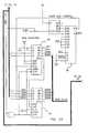
- FIG. 1shows a schematic diagram of the video display adjustment and on-screen menu system 10 in accordance with the present invention.
- the system 10comprises three principle functional blocks: an input, memory storage and controller block 12, a video display adjustment block 14 and a character display block 16.
- an input, memory storage and controller block 12either a front panel 18 or a PC connector 20 can be used to input adjustment selections to the system 10.
- These inputsare temporarily buffered in an input latch 22.
- a microcontroller 24accepts these inputs from the input latch 22, and stores changes to the video display parameters in an EEPROM memory storage area 25.
- certain display parameters provided by the microcontrollerare buffered by an output latch 26.
- the majority of the display parametersare sequentially sent to a DAC 28 that converts the parameters to analog signals.
- These analog signalsare demultiplexed by a series of analog switches 30 enabled after every vertical sync pulse.
- the signals of each switch 30are stored by a complementary series of sample-and-hold circuits 32. These circuits hold the parameters for display operation until new parameters are provided.
- the third block, the character display block 16,generates and sends on-screen menu information to the video display synchronized to the display's horizontal frequency.
- the column counters 34increment for each pixel being sent divided by the number of pixels per character. In the preferred embodiment, each character is 8 pixels across, so the column counters 34 divide the video clock signal by eight. When the column counters 34 reach their end, the current line of the menu has been reached.
- a character size control block 36decides whether to repeat the current pixel line (essentially elongating a character). Because higher horizontal frequencies indicate an increased vertical resolution of the display screen, repeating individual character lines increases their vertical size. Characters in the preferred embodiment are created on an 8 by 8 grid, and then each pixel line is doubled, to create an 8 by 16 displayed character.
- each pixel line of a characteris doubled once more to create an 8 by 32 displayed character.
- the character size control blockallows the row counters 38 to increment to the next pixel line of the characters in the menu.
- a display memory 40holds the current array of character codes that make up the displayed menu. Every eight video clock ticks, the column counter 34 increments to indicate the next character code in the current menu line. Every 16 (or if doubled, 32) horizontal sync pulses (scan lines), the row counters 38 increment the display memory 40 to the next fun line of character codes in the current menu.
- the current character code(in ASCII) pointed to in the display memory 40 by the column and row counters 34 and 38 refers to character display information stored in a character PROM memory 42. Every horizontal sync pulse, the row counters 34 indicate which pixel line of the current character display information is read out of the character PROM 42. These pixel lines are repeated 2 or 4 times depending on the horizontal frequency, as described.
- the pixel line for each character in the current embodimentis 8 pixels wide and is stored in a shift register 46, where it is clocked out to a video drive 48.
- the video drive 48blanks the current space on the video screen and replaces the video display with the current pixel line of character display information.
- a video clock 44provides the appropriate video clock information to the column counters 34, the row counters 36 and the shift register 46 for synchronizing the output of each pixel of menu information.
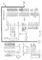
- FIGS. 2, 3 and 4present circuit schematics of the present invention that describe its construction and operation in greater detail.
- FIG. 2reveals most of the video display adjustment and on-screen menu system 10.
- the front panel 18 in the preferred embodimentcomprises a series of switches having outputs labeled Reset, Up, Down and Select. Reset resets all user adjustments to factory preset conditions, Select selects adjustments from the on-screen menu, Up increments an adjustment, and Down decrements an adjustment.
- These switch-provided inputscan be complemented by a series of direct inputs from a PC connector 20, allowing direct input to the menu system from an automated factory adjustment system.
- the inputsare buffered by an input latch 22, comprising a 74LS373 octal transparent latch with 3-state outputs.
- the microcontroller 24reads information from the input latch through its ports P0.1 through P0.7 whenever LAT1 is enabled.
- the horizontal sync (HS) and vertical sync (VS) signalsare also sent through the input latch 22 to the microcontroller 24, which determines whether they are present and their polarities. If HS and VS are not present then either SOG or a composite sync signal is used.
- the HS signalis sent to the INTO port of microcontroller 24 since its pulse width can be too small to be detected by the microcontroller 24 otherwise.
- the monitorcan receive sync information in three ways: (a) separate horizontal and vertical sync signals; (b)a composite sync signal (where the horizontal and vertical sync are added together into one sync signal); and (c) a Sync On Green (SOG) signal, where the composite sync signal is added to the GREEN signal.
- the microcontroller 24determines which of the three types of sync signal is being sent, then generates the SOG and CMPS signal to let the corresponding circuits know what is being sent.
- the microcontroller 24preferably employs a 80C51 CMOS 8-bit CPU and a 16MHz oscillator. In addition to controlling the on-screen menu system and the CRT display parameters, the microcontroller 24 creates the pin-cushion correction waveform for the display. A 16MHz oscillator was chosen to provide the necessary bandwidth to synthesize the waveform.
- the signals used throughout the invention as inputs and outputs of the microcontroller 24have the following meanings: INT0 is an external interrupt activated by a high-to-low transition of the vertical sync signal, that lets the microcontroller 24 know when to start generating the pin-cushion signal. Therefore, the preferred embodiment uses a negative vertical sync signal.
- the INT0 inputis also used to determine if the monitor is running synchronization on green and the horizontal sync HS. This alternative procedure occurs when the input latch 22 is enabled and the HS signal passes through to INT0.
- An inverter 49is used to invert the VS signal and provide an open collector output to share with the input latch's HS output.
- the inverted signals HS' and VS'are always positive going horizontal and vertical synchronization pulses.
- INT1provides an output signal WEEP* that is the chip enable command for the EEPROM memory 25 when reading and writing to the EEPROM 25.
- the T0 inputreceives the HS' signal, allowing the microcontroller 24 to count the number of scan lines. The number of lines is used by the pin generation algorithm, and also to look up appropriate display parameters for a new horizontal frequency and then output these new parameters to the display.
- T1provides the CRTD output signal that is logical 1 when the on-screen menu is enabled.
- Port P1.0-7is an eight-bit data port that outputs the display parameter signals (including the pin-cushion waveform) to the DAC 28.
- the RXD pinoutputs a CLRL signal that clears the row counters 38.
- This methodis used for ease of programming and speed. There are only two dead periods during the display tracing where the pin-cushion waveform is not generated: during vertical retrace and in the center of the display. Two separate displays are shown during the on-menu operations of the present invention: a main menu, and a smaller Value Indicator Graph (VIG) that graphically represents the increments and decrements made by a user to a given display parameter (such as brightness). There is enough time in the center of the trace to allow the VIG to be erased and re-written to the screen while keeping the display steady. When the main menu is being displayed, however, there is not enough time even during the center portion of the trace. Therefore, the present invention rewrites the main menu in two complete trace cycles. First the menu is cleared from the SRAM display memory area 40 in one cycle, and then is written in the next cycle, when the row counters 38 are also cleared.
- VOGValue Indic
- the TXD pinoutputs the WRAM* signal which is the SRAM write enable signal, for writing to the display memory 40.
- the ALE pinoutputs the Address Latch Enable (ALE) signal which is the general read/write enable signal generated by the microcontroller 24 for reading and writing all external RAM and ROM memories (such as EEPROM 25 and display memory 40).
- ALEAddress Latch Enable
- the WR* signalis the write enable command generated by the microcontroller 24 for writing to external RAM and ROM memories, while the RD* signal is the read enable command for reading these external memories.
- LAT0is used to control the output latch 26
- LAT1is used to control the input latch 22.
- AS0*, AS1* and AS2*enable analog switches 0, 1 and 2 respectively (analog switches 30A, B and C).
- the rest of port P2 (P2.0 through P2.2) along with port P0 (P0.0 through P0.7)provides an 11-bit data and address bus DBO-10 for accessing external RAM and ROM through the invention.
- DB0-5connect to the output latch 26 comprising a 74LS174 hex D Flip-Flop integrated circuit.
- Output latch 26stores several of the display parameters that are changed whenever a new video mode is present.
- the stored parameters of the output latchare changed by enabling LAT0 upon recognizing the new video mode, latching the outputs of PO.0-5 (via DB0-5) to the outputs of the output latch.
- the CMPS signalis 1 if no VS signal is present, indicating a composite video signal.
- the SL0 signalcontrols the size of the characters displayed. If SL0 equals 0, each character has an 8 by 16 cell. If SL0 equals 1, the cell is 8 by 32. The SL0 signal is sent to the character size control block 36 discussed further below.
- Signals SC0-2comprise a 3-bit signal indicating the horizontal frequency. If the signals SC0-2 equal 7, the frequency is 30khz, if the signals SC0-2 equal 0, the frequency is 75khz. All other values proportionately divide up the frequency spectrum between these two extremes. The SC0-2 values can then be used to switch in S capacitors for different frequencies to keep acceptable horizontal linearity of the display. The use of S capacitors for this purpose is well known to those skilled in the art.
- the EEPROM chip 25 used in the preferred embodimentis an XL2816AP-250 that is rated for a minimum of 10,000 writes per byte of memory.
- the EEPROM 25stores all the video display adjustment settings.
- the chip select (WEEP*), read enable (RD*) and write enable (WR*)are controlled by the microcontroller 24 as discussed above.
- the EEPROM chip 25 outputs D0-7are sent to the P0 port of the microcontroller 24.
- the address lines for the EEPROM chip 25come from the column and row counter outputs COL 0 through COL 4 and ROW 0 through ROW 5.
- the present inventionuses the column and row counters 34 and 38 also as address latches for addressing the EEPROM 25.
- the particular chips chosen for the column and row counters 34,38are presettable, allowing them to function as these latches.
- DB0-10loads the EEPROM read/write address into the column and row counters 34 and 38, enabled by the ALE signal. Then, the counters' outputs address the appropriate byte of EEPROM memory while DB0-7 reads or writes that byte's data.
- the digital-to-analog (DAC) block 28receives its 8-bit digital signal from port P1 of microcontroller 24, and converts the signal to analog form to provide to the analog switches 30 and their respective sample-and-hold circuits 32.
- the DAC 28provides a ⁇ 1% linearity with a linear change in digital input. While the schematic of Figure 2 illustrates the DAC 28 comprising discrete components, an appropriate integrated DAC can be substituted.
- An 74LS05 hex inverter ICprovides an open collector hex inverter since the P1 outputs of the microcontroller 24 are not truly open collector and can cause non-linearities.
- the specifications of the particular componentsare as shown in FIG. 2.
- the output VADJ of the DAC 28connects with three analog switches 30.
- each analog switch 30comprise a CD4051B single 8 channel analog multiplexer.
- the single DAC output VADJdrives the three separate analog switches 30 to provide 24 separate adjustments.
- Each respective analog switch 30A, B and Cis switched to on via signals AS0-2.
- Data bus lines DB8-10then select 1 of 8 output lines of the analog switch to enable.
- all 24 adjustmentsare updated by sequentially turning on each analog switch and then, in turn, that switch's separate output lines S0-7, T0-7 and U0-7.
- Each circuitreceives one line from a given analog switch 30.
- switch 32greceives signal S6 from analog switch 30a. The signal S6 is turned on when AS0* is high, and DB8-10 reads "110".
- Switch 32gprovides the Focus adjustment for the display. All the switch outputs, connections and truth tables are provided below in Table 1.
- the character display block 16provides the on-screen menus and value indicator graphs for changing the display parameters.
- the display of the menusis regulated by the column and row counters 34 and 38.
- Column counters 34preferably comprise chained 74F161 synchronous presettable binary counters.
- the first three output lines AD0-2clock the eight pixels of each character pixel line and latch data from the character PROM 42 to the Shift Register 46.
- the higher-level signal lines COL0-COL4address the display memory 40, indicating which character on the current menu line is active.
- the final output, RCOindicates that the 32 columns of the menu line have been completed, and temporarily stops the video oscillator clock 44, until the next horizontal sync signal HS activates the clock again.
- the CLK signal for the countersis generated by the video oscillator clock 44.
- the column and row counters 34 and 38double as address latches for reading and writing the EEPROM 25.
- the ALE signalis substituted for the CLK signal.
- the row counters 38are also formed from chained 74LS161 synchronous presettable binary counters.
- the first 2 outputs of the row counters LNE1-2are sent to the character PROM's second and third input bits, since each character has eight lines and each line is at least doubled (and sometimes quadrupled).
- LNE0(which attaches to the character PROM's first input, comes directly from the character size control block 36, discussed further below.
- the remaining output signals ROW0-5address the display memory block 40, determining which row of character to display. Again, since the counters double as address latches for reading and writing the EEPROM 25, the data is latched using ALE instead of the CLK signal.
- the character size control block 36sits functionally between the column counters 34 and the row counters 38. During menu display, as the columns for a given row (of character pixel line information) are exhausted, the character size control block determines whether to advance the row counters to the next row. In lower horizontal frequencies, each line of a character is doubled: i.e ., the column counters cycle through two complete cycles of the same character line before advancing the row counters. At higher frequencies, when characters would appear squashed, the character size control block 36 retards the row counter advance for four complete column cycles. The character size control block 36 counts horizontal rows by using the HC* signal from the column counter block 34, which is the same as the horizontal sync signal HS.
- the character size control block 36preferably comprises a 74LS393 dual 4 stage binary counter and a 74LS151 8 input multiplexer, as indicated in FIG. 2.
- the LCL signal lineis the clock line for the row counters.
- the addresses generated by the column and row counters 34 and 38are sent to the display memory block 40, comprising 2 1K by 4 static RAM 2114AL-2 chips.
- ROW0-4are the row address lines, allowing 32 possible menu rows to be stored
- COL0-4are the column address lines, allowing 32 characters per row.
- DB0-7are the data input lines from the microcontroller 24 that can store characters for each address location.
- Outputs DB0-5connect to the character PROM 42 to indicate which character to display, while outputs DB6-7 connect to the video drive 48 to cause appropriate video blanking and color for the menu.
- the WRAM* signalis the write enable for the display memory SRAMs, and the microcontroller WR* signal connects to each chip's CS* pin.
- the WEEP* signalis 0 if writing to the EEPROM 25, such that no writing is done to the display memory 40.
- the systemis capable of displaying 32 rows, a maximum of 16 rows can be displayed before the VS signal clears the counter. To assure that the display is always in the horizontal active area, only columns 8 through 24 are used. Also, due to speed limitations of the microcontroller 24, only 5 rows are used.
- the character PROM memory block 42comprises a 74S472 512-by-8 byte TTL PROM.
- Signals LN0-2comprise the 3-bit character line address (providing 8 lines per character) that comes from the row counters 38.
- Signals DB0-5comprise the 6 bit character address (allowing 64 possible characters) from the display memory block 40.
- Data lines O1-8provide the character pixel line information (having 8 pixels per character line) latched from the character PROM memory block 42 to the shift register block 46 for output to the video display.
- DB0-5determine which character to display, while LN0-2 determine which line of that character to output.
- the character PROM 42outputs the 8 pixels of the current pixel line of the current character.
- the video clock 44provides the coordinating timing mechanism for the character display section 16.
- the clock 44is a variable oscillator that is synchronized to the incoming horizontal frequency.
- the clock's frequencyis controlled by varying an OSV voltage (determined by microcontroller 24 and stored by S/H circuit 32e) such that character size is kept fairly constant, regardless of horizontal frequency.
- the oscillatoris kept synchronous to the horizontal frequency to maintain the menu information stationary on the video display.
- the video clock frequencyis varied by controlling the constant current source to the oscillator by varying OSV.
- the clockis synchronized to the horizontal frequency by gating the horizontal sync signal HS with the oscillator, starting the oscillator when each horizontal line occurs.
- the clockis turned off when the columns for the display complete their cycle for one line.
- the OSV signalis an analog 10-15V signal stored by S/H circuit 32e.
- RCO from counter U10goes high when the counters reach FF (their end) and kills the video clock by using a 74LS393 as a latch.
- the horizontal sync signal HS'restarts the clock by clearing this 74LS393 latch.
- the output CLKdrives the counters 34 and 38, while the inverse output CLK* drives shift register 46.
- Table 3presents a truth table relating these signals.
- the video clock 44uses a 74F132 quad 2 input NAND Schmitt trigger, a 74LS02 Quad 2 input NOR gate, and other discrete components as indicated.
- the clock outputis between 10 and 20 Mhz dependent on incoming horizontal frequency.
- the clock's frequencypreferably defaults to be proportional to the horizontal frequency. However, the user can also adjust the oscillator frequency for each mode by making selections on the menu, thereby controlling the horizontal size of the characters.
- the shift register 46is a 74F166 8 bit shift parallel-to-serial register.
- Data lines O1 8 from the character PROM 42provide the video information to the shift register (the current pixel line for the current character).
- the CLK* signal from the video clock 44shifts the data to the output one bit at a time.
- AD0-2are from the column counters 34 that latches a new set of pixel information every 8 video clock ticks, loading the next character's pixel line.
- Zis the video signal output sent to the video drive 48.
- the video drive block 48drives transistor amplifiers on the video display's driver circuitry.
- the video information normally sent to the video displayis blanked for an entire character whenever character information is written to the display during menu operation. All other times, the normal video information is sent to the video display.
- the video drive block 48employs three 74LS08 Quad 2 input AND gates.
- the Z lineis the video signal from the shift register, signal DB6 allows the Z signal to also drive the blue video signal, and signal DB7 is from the display memory block and blanks the PC's video for 1 character cell.
- the CRTD* signalis used to avoid false triggers: the system only blanks a character cell when this signal is active.
- RGDis the video signal drive for the red and green video signals.
- BDis the blue video signal, and BLANK blanks the RGB video signal sent from the computer that normally drives the display.
- the sequential operation of the present inventionis described in flow chart 50 of FIG. 5.
- the initial conditions for the displayare read 52 by the microcontroller 24 from the EEPROM memory 25 and sent via the DAC 28 and digital switches 30 to the individual sample-and-hold circuits 32.
- the microcontroller 24counts the number of horizontal lines traced and determines 54 if the number of lines differ from the previous count. If not, the microcontroller asks 56 whether the user has started to make any adjustments. If that is also not true, the microcontroller determines 58 if the reset button on the front panel 18 has been pressed. If the answer is also false, the microcontroller begins generating the top of the pincushion waveform 60. If any menu is being displayed, its contents are written 62 at the middle of the display trace to the display memory block 40. Then the microcontroller 24 generates the bottom of the pincushion waveform 64.
- the microcontroller 24updates all S/H circuits 32, clears the menu display and counters 34, 38 and 40, and counts the number of horizontal lines again. If the line count is different, a different horizontal frequency is being used. The microcontroller 24 then determines 68 the horizontal frequency, the vertical frequency and the polarities of the signals. Having determined which new frequency mode is being used, the menu system then reads the appropriate display parameters 70 from the EEPROM memory 25. These display parameters are then converted and sent 72 to the S/H circuits 32, and the microcontroller 24 begins the normal operation of generating the pincushion waveform in steps 60 through 66.
- the microcontroller 24changes the appropriate adjustment value, both in the EEPROM memory 25, and at the next vertical retrace 66, the appropriate S/H circuit 32. If the user presses the Reset button at step 58, the microcontroller 24 reads 74 the appropriate EEPROM memory for the factory-default standards for the current frequency mode. Meanwhile, the normal operation of generating the pincushion waveform, displaying the menu display, and updating the S/H circuits 32 at the vertical sync signal occur as before in steps 60 through 66.
Landscapes
- Engineering & Computer Science (AREA)
- Physics & Mathematics (AREA)
- Computer Hardware Design (AREA)
- General Physics & Mathematics (AREA)
- Theoretical Computer Science (AREA)
- Radar, Positioning & Navigation (AREA)
- Remote Sensing (AREA)
- Controls And Circuits For Display Device (AREA)
- Transforming Electric Information Into Light Information (AREA)
- Television Receiver Circuits (AREA)
Description
- The present invention relates to video display systems, and more particularly, to an apparatus for adjusting videodisplay controls in a multi-frequency video display according to the preamble of
claim 1. An apparatus of this type isdisclosed in WO 89/00325. This reference describes a method and apparatus by which horizontal and vertical synchronizingsignals from a video source are evaluated to determine which of a plurality of stored operating modes areto be selected for a particular multi-frequency monitor. A separate display unit is provided which is connected to amicrocomputer for receiving and storing the user input for video display controls and for controlling the synchronizingsignals. - The GB-A-2 155 714 discloses a television system where an on-screen character generator can display a numberedlist or menu of various functions to be controlled. A particular function can be selected by pressing a correspondinglynumbered key. Adjustments of video display controls, however, cannot be represented with the system of thisdocument.
- Video displays incorporating CRT systems provide information to and receive information from computer systems.The versatility of CRT systems, and the variety of ways they display data, have ensured their widespread use. Earlyvideo displays typically were single-frequency displays: the video adaptor card that operated the display (by sendinginformation from the computer to the display) used a single horizontal scanning frequency tuned to that of the display.A card fabricated for a particular single-frequency display often will not work with other displays. Multi-frequency videodisplays represent an important improvement in video display technology, for a single display system can be attachedto a wide variety of video adaptor cards. The multi-frequency display can tune itself to the horizontal frequency of theattached adaptor card, and synchronize the display to the information sent from the adaptor card.
- While multi-frequency displays provide a great improvement over single-frequency displays, and allow versatileconnections of displays and adaptor cards, these displays exacerbate problems common to video displays in general.Most video displays provide some form of adjustments for users. Typically, a panel of knobs and buttons connected topotentiometers or other electrical switches allow the user to adjust various display characteristics. Contrast, brightness,and the horizontal and vertical image positions are some of the possible adjustments one can make. Since theseadjustments are made manually using electromechanical devices, the adjustments are susceptible to slight shifts overtime. Movement of the display, changes in ambient temperature and environmental vibrations can all alter carefully setadjustments.
- Multi-frequency displays that incorporate electromechanical user adjustments share these problems of misadjustment.In addition, these displays multiply adjustment problems for each new frequency mode available. Each time auser changes the frequency mode used by the monitor, all the adjustments made previously must be readjusted tocompensate for changes in the display. Furthermore, once these changes are adjusted, they again become susceptibleto slow misadjustment.
- Whereby it is known from GB-A-2 155 714 an onscreen display for adjusting parameters (such as brightness)of a common TV screen (see this
document page 1,lines 48 to 65). It is known from US-A-4,991,023 anapparatus for adjusting video display controls in a multi-frequency video display. The display is tuned to thefrequency of the horizontal sync signal of a wide variety of video adaptor cards of computer systems. It has ascreen for displaying information received from these computer systems. The apparatus comprises an inputcontrol block for providing user input; a micro controller capable of receiving said user input from said inputcontrol block and controlling the adjustment of the video display controls; a memory block being capable ofstoring parameters of said adjusted video display controls, this memory block being electrically connected tosaid micro controller; and a display adjustment block capable of providing the parameters of the adjusted videodisplay controls to the multi-frequency video display in order to set the video display controls, this display adjustmentblock being coupled to and controlled by said micro controller and thus this document discloses thefeatures of the preamble ofclaim 1. - Document "A multi-systems onscreen display for TV MCU" by G.K. Lunn et.al., IEEE Transactions onConsumer Electronics, Vol. 35, No. 4, 1989, pp. 803-809, describes an onscreen display system (OSD system)for a TV which is compatible with different scanning standards and it is mentioned in this document that thecharacters displayed on the TV screen can be kept constant over non-standard horizontal frequencies by makingthe character pixel read-out rate proportional to the horizontal sync frequency.
- Multi-frequency displays present further manufacturing difficulties. In addition to user-operated external controls,each video display possesses a number of internal controls that precisely adjust the display. These internal controlsare preset at the factory by a human operator comparing the display against a standard. To ensure comparable operationacross frequency modes, multi-frequency displays often have separate sets of these adjustments for each ofseveral principle frequency bands. Each of these adjustment sets must then be hand-adjusted by a factory operator.Again, the electro-mechanical nature of the controls allows for gradual drift in their adjustment.
- Current methods for adjusting video displays, particularly in multi-frequency systems, do not provide a completeand flexible system for allowing users and manufacturers to quickly and reliably set display controls. What is neededis an improved method and apparatus for adjusting video displays. An improved video display adjustment apparatusand method should allow the factory to quickly set all internal controls for a monitor, without operator intervention. Theimproved apparatus and method should also allow end-users to easily change display characteristics, or reset thecharacteristics back to those specified at the factory. The method and apparatus should also maintain the video displaycharacteristics despite thermal, mechanical or other environmental changes. The improved method and apparatusshould provide techniques and apparatus applicable to a wide range of video display devices, including CRTs, LCDsand electro-luminescent displays. The invention should provide a simple and cost-effective technology for easily andaccurately changing and maintaining the characteristics of any video display.
- According to the present invention an apparatus for adjusting of video display controls in a multi-frequencyvideo display comprising the features of
claim 1 and a method for adjusting video display controls ina multi-frequency video display comprising features ofclaim 7 are provided. - In accordance with the present invention, a video display adjustment and on-screen menu system combines amicrocontroller and erasable EPROM memory with on-screen menu display generation to allow users to change displayparameters without making any electromechanical adjustments. The microcontroller effects display changes through display adjustment circuitry, enabling digital control over display parameters. In addition, the present invention incorporatesa novel video clock to ensure accurate synchronization of the on-screen menu to any horizontal signal receivedby the video display.
- The user enters commands to the microcontroller by pressing a set of buttons, or other similar input devices onthe video display, in response to selections displayed by the on-screen menu. User commands are latched and accessedby the microcontroller; and changes to display parameters made by the user are written to an EEPROM memorythat in the preferred embodiment can store a set of adjustments for each of up to 32 possible operational frequencymodes.
- The display adjustment circuitry includes a digital-to-analog converter (DAC) that converts display parametersprovided by the microcontroller in digital form to an analog signal that is multiplexed via a set of analog switches to aplurality of sample-and-hold circuits. Upon start-up, these circuits are loaded with and maintain current display parameters,until changed by the user.
- The on-screen menu generation circuitry includes a set of column and row counters that keep track of the nextmenu location to be displayed. Because higher horizontal frequencies indicate higher resolutions, the characters ofthe menu are adjusted to maintain a relatively constant character size. The microcontroller determines how manyvertical lines are being displayed, and then a character size control block determines whether to double the numberof times a pixel line of a given character is repeated, essentially elongating the character. When a line repeats, the rowcounter does not increment despite the fact that another horizontal synch signal was received. The current columnand row values address a display memory, loaded by the microcontroller, that contains the menu information. As eachmenu character is read out of the display memory at the appropriate column and row, its visual representation isprovided by a character PROM and then sent to a shift register where each pixel is clocked out to a video drive.
- The video clock governs the operation of the column and row counters, and that of the shift register, and therebythe flow of menu information to the display. The novel video clock of the present invention stops operation for a givenscan line when the end of the column counters are reached for each menu line. The video clock resumes its operationwhen the next horizontal synch signal occurs. In this way, the menu remains intact and readable regardless of whathorizontal frequency the display currently uses.
- The present invention allows users to easily and precisely adjust the parameters of a multi-frequency video displaywithout adjusting electromechanical inputs. Once parameters are chosen and stored for a given frequency, they canbe retrieved and employed by the microcontroller on starting up the video display. Furthermore, a number of differentparameter sets can be stored, such that changing video display frequencies automatically restores the appropriateparameter set without further user input. Since all parameters are stored digitally, display parameters can be easilyreset to factory standards if desired. Moreover, each parameter set will not degrade with time or environmental changes.
- The present invention also provides an easy method for adjusting display parameters in the factory, during assemblyand testing. By providing a PC connection port (in addition to the front panel user input), each display can beconnected to an automated testing station. A testing station might include a video camera, display cards for displayingtest patterns on screen, and a computer controller. The testing station can cycle through a series of tests for differentdisplay frequencies, adjusting all internal controls electronically through the PC connection port. Each group of adjustmentswould then be stored as a factory-standard parameter set.
- The methods and apparatus of the present invention provide novel techniques for adjusting and storing sets ofparameters for multi-frequency displays. The methods of storing parameters in EEPROM memory, and retrieving parametersusing a microcontroller, allows display parameters to be adjusted for each horizontal synch frequency. Usingsimple user input buttons, and a programmable on-screen menu, the present invention avoids making adjustmentsusing fallible, imprecise electromechanical devices. The apparatus and methods of the present invention provide forsynchronizing the menu display regardless of the horizontal synchronization frequency. In addition, the present inventionprovides for adjustable menu character sizes across frequencies. The methods and apparatus of the presentinvention provide easily implemented, compact, inexpensive devices for adjusting the display characteristics of multi-frequencyvideo displays, both during assembly in the factory and during operation by the user. These and other featuresand advantages of the present invention are apparent from the description below with reference to the following drawings.
- Figure 1 shows a block diagram of a video display adjustment and on-screen menu system in accordance withthe present invention.
- Figure 2 shows a circuit diagram of a video display adjustment and on-screen menu system in accordance withthe present invention.
- Figure 3 shows a circuit diagram of a analog switch and associated sample and hold circuits.
- Figure 4 shows a circuit diagram of several analog switches and associated sample and hold circuits.
- Figure 5 shows a flow chart of the operation of the present invention.
- In accordance with the present invention, FIG. 1 shows a schematic diagram of the video display adjustment andon-
screen menu system 10 in accordance with the present invention. Thesystem 10 comprises three principle functionalblocks: an input, memory storage andcontroller block 12, a videodisplay adjustment block 14 and acharacterdisplay block 16. Within the input, memory storage andcontroller block 12, either afront panel 18 or aPC connector 20 can be used to input adjustment selections to thesystem 10. These inputs are temporarily buffered in aninput latch 22. Amicrocontroller 24 accepts these inputs from theinput latch 22, and stores changes to the video display parametersin an EEPROMmemory storage area 25. - Within the video
display adjustment block 14, certain display parameters provided by the microcontroller are bufferedby anoutput latch 26. The majority of the display parameters are sequentially sent to aDAC 28 that converts theparameters to analog signals. These analog signals are demultiplexed by a series of analog switches 30 enabled afterevery vertical sync pulse. The signals of eachswitch 30 are stored by a complementary series of sample-and-holdcircuits 32. These circuits hold the parameters for display operation until new parameters are provided. - The third block, the
character display block 16, generates and sends on-screen menu information to the videodisplay synchronized to the display's horizontal frequency. The column counters 34 increment for each pixel being sentdivided by the number of pixels per character. In the preferred embodiment, each character is 8 pixels across, so thecolumn counters 34 divide the video clock signal by eight. When the column counters 34 reach their end, the currentline of the menu has been reached. A charactersize control block 36 then decides whether to repeat the current pixelline (essentially elongating a character). Because higher horizontal frequencies indicate an increased vertical resolutionof the display screen, repeating individual character lines increases their vertical size. Characters in the preferredembodiment are created on an 8 by 8 grid, and then each pixel line is doubled, to create an 8 by 16 displayed character.At higher frequencies, each pixel line of a character is doubled once more to create an 8 by 32 displayed character.Once a set of repetitions of a character's pixel line are completed, the character size control block allows the rowcounters 38 to increment to the next pixel line of the characters in the menu. - A
display memory 40 holds the current array of character codes that make up the displayed menu. Every eightvideo clock ticks, the column counter 34 increments to indicate the next character code in the current menu line. Every16 (or if doubled, 32) horizontal sync pulses (scan lines), the row counters 38 increment thedisplay memory 40 to thenext fun line of character codes in the current menu. The current character code (in ASCII) pointed to in thedisplaymemory 40 by the column and row counters 34 and 38 refers to character display information stored in acharacterPROM memory 42. Every horizontal sync pulse, the row counters 34 indicate which pixel line of the current characterdisplay information is read out of thecharacter PROM 42. These pixel lines are repeated 2 or 4 times depending onthe horizontal frequency, as described. The pixel line for each character in the current embodiment is 8 pixels wideand is stored in ashift register 46, where it is clocked out to avideo drive 48. The video drive 48 blanks the currentspace on the video screen and replaces the video display with the current pixel line of character display information.Avideo clock 44 provides the appropriate video clock information to the column counters 34, the row counters 36 andtheshift register 46 for synchronizing the output of each pixel of menu information. - FIGS. 2, 3 and 4 present circuit schematics of the present invention that describe its construction and operationin greater detail. FIG. 2 reveals most of the video display adjustment and on-
screen menu system 10. Thefront panel 18 in the preferred embodiment comprises a series of switches having outputs labeled Reset, Up, Down and Select.Reset resets all user adjustments to factory preset conditions, Select selects adjustments from the on-screen menu,Up increments an adjustment, and Down decrements an adjustment. These switch-provided inputs can be complementedby a series of direct inputs from aPC connector 20, allowing direct input to the menu system from an automatedfactory adjustment system. The inputs are buffered by aninput latch 22, comprising a 74LS373 octal transparent latchwith 3-state outputs. Themicrocontroller 24 reads information from the input latch through its ports P0.1 through P0.7whenever LAT1 is enabled. The horizontal sync (HS) and vertical sync (VS) signals are also sent through theinputlatch 22 to themicrocontroller 24, which determines whether they are present and their polarities. If HS and VS arenot present then either SOG or a composite sync signal is used. The HS signal is sent to the INTO port ofmicrocontroller 24 since its pulse width can be too small to be detected by themicrocontroller 24 otherwise. The monitor can receivesync information in three ways: (a) separate horizontal and vertical sync signals; (b)a composite sync signal (wherethe horizontal and vertical sync are added together into one sync signal); and (c) a Sync On Green (SOG) signal, wherethe composite sync signal is added to the GREEN signal. Themicrocontroller 24 determines which of the three typesof sync signal is being sent, then generates the SOG and CMPS signal to let the corresponding circuits know what isbeing sent. - The
microcontroller 24 preferably employs a 80C51 CMOS 8-bit CPU and a 16MHz oscillator. In addition to controllingthe on-screen menu system and the CRT display parameters, themicrocontroller 24 creates the pin-cushion correction waveform for the display. A 16MHz oscillator was chosen to provide the necessary bandwidth to synthesizethe waveform. The signals used throughout the invention as inputs and outputs of themicrocontroller 24 have thefollowing meanings: INT0 is an external interrupt activated by a high-to-low transition of the vertical sync signal, thatlets themicrocontroller 24 know when to start generating the pin-cushion signal. Therefore, the preferred embodimentuses a negative vertical sync signal. The INT0 input is also used to determine if the monitor is running synchronizationon green and the horizontal sync HS. This alternative procedure occurs when theinput latch 22 is enabled and the HSsignal passes through to INT0. An inverter 49 is used to invert the VS signal and provide an open collector output toshare with the input latch's HS output. The inverted signals HS' and VS' are always positive going horizontal and verticalsynchronization pulses. INT1 provides an output signal WEEP* that is the chip enable command for theEEPROMmemory 25 when reading and writing to theEEPROM 25. - The T0 input receives the HS' signal, allowing the
microcontroller 24 to count the number of scan lines. The numberof lines is used by the pin generation algorithm, and also to look up appropriate display parameters for a new horizontalfrequency and then output these new parameters to the display. T1 provides the CRTD output signal that is logical 1when the on-screen menu is enabled. Port P1.0-7 is an eight-bit data port that outputs the display parameter signals(including the pin-cushion waveform) to theDAC 28. - The RXD pin outputs a CLRL signal that clears the row counters 38. This method is used for ease of programmingand speed. There are only two dead periods during the display tracing where the pin-cushion waveform is not generated:during vertical retrace and in the center of the display. Two separate displays are shown during the on-menu operationsof the present invention: a main menu, and a smaller Value Indicator Graph (VIG) that graphically represents theincrements and decrements made by a user to a given display parameter (such as brightness). There is enough timein the center of the trace to allow the VIG to be erased and re-written to the screen while keeping the display steady.When the main menu is being displayed, however, there is not enough time even during the center portion of the trace.Therefore, the present invention rewrites the main menu in two complete trace cycles. First the menu is cleared fromthe SRAM
display memory area 40 in one cycle, and then is written in the next cycle, when the row counters 38 arealso cleared. - The TXD pin outputs the WRAM* signal which is the SRAM write enable signal, for writing to the
display memory 40. The ALE pin outputs the Address Latch Enable (ALE) signal which is the general read/write enable signal generatedby themicrocontroller 24 for reading and writing all external RAM and ROM memories (such asEEPROM 25 anddisplay memory 40). The WR* signal is the write enable command generated by themicrocontroller 24 for writing toexternal RAM and ROM memories, while the RD* signal is the read enable command for reading these external memories. - LAT0 is used to control the
output latch 26, LAT1 is used to control theinput latch 22. AS0*, AS1* and AS2* enableanalog switches output latch 26 comprising a 74LS174 hex D Flip-Flop integratedcircuit.Output latch 26 stores several of the display parameters that are changed whenever a new video mode ispresent. The stored parameters of the output latch are changed by enabling LAT0 upon recognizing the new videomode, latching the outputs of PO.0-5 (via DB0-5) to the outputs of the output latch. The CMPS signal is 1 if no VSsignal is present, indicating a composite video signal. The SL0 signal controls the size of the characters displayed. IfSL0 equals 0, each character has an 8 by 16 cell. If SL0 equals 1, the cell is 8 by 32. The SL0 signal is sent to thecharactersize control block 36 discussed further below. - Signals SC0-2 comprise a 3-bit signal indicating the horizontal frequency. If the signals SC0-2 equal 7, the frequencyis 30khz, if the signals SC0-2 equal 0, the frequency is 75khz. All other values proportionately divide up thefrequency spectrum between these two extremes. The SC0-2 values can then be used to switch in S capacitors fordifferent frequencies to keep acceptable horizontal linearity of the display. The use of S capacitors for this purpose iswell known to those skilled in the art.
- The
EEPROM chip 25 used in the preferred embodiment is an XL2816AP-250 that is rated for a minimum of 10,000writes per byte of memory. TheEEPROM 25 stores all the video display adjustment settings. The chip select (WEEP*),read enable (RD*) and write enable (WR*) are controlled by themicrocontroller 24 as discussed above. TheEEPROMchip 25 outputs D0-7 are sent to the P0 port of themicrocontroller 24. The address lines for theEEPROM chip 25come from the column and rowcounter outputs COL 0 throughCOL 4 andROW 0 throughROW 5. To minimize thenumber of separate components, the present invention uses the column and row counters 34 and 38 also as addresslatches for addressing theEEPROM 25. The particular chips chosen for the column and row counters 34,38 (discussedbelow) are presettable, allowing them to function as these latches. First, DB0-10 loads the EEPROM read/write addressinto the column and row counters 34 and 38, enabled by the ALE signal. Then, the counters' outputs address theappropriate byte of EEPROM memory while DB0-7 reads or writes that byte's data. - The digital-to-analog (DAC)
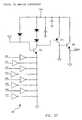
block 28 receives its 8-bit digital signal from port P1 ofmicrocontroller 24, and convertsthe signal to analog form to provide to the analog switches 30 and their respective sample-and-hold circuits 32. TheDAC 28 provides a <1% linearity with a linear change in digital input. While the schematic of Figure 2 illustrates theDAC 28 comprising discrete components, an appropriate integrated DAC can be substituted. An 74LS05 hex inverterIC provides an open collector hex inverter since the P1 outputs of themicrocontroller 24 are not truly open collectorand can cause non-linearities. The specifications of the particular components are as shown in FIG. 2. The outputVADJ of theDAC 28 connects with three analog switches 30. - Referring now to figures 3 and 4, each
analog switch 30 comprise a CD4051B single 8 channel analog multiplexer.The single DAC output VADJ drives the three separate analog switches 30 to provide 24 separate adjustments. Eachrespective analog switch 30A, B and C is switched to on via signals AS0-2. Data bus lines DB8-10 then select 1 of 8output lines of the analog switch to enable. At the beginning of each vertical sweep, all 24 adjustments are updatedby sequentially turning on each analog switch and then, in turn, that switch's separate output lines S0-7, T0-7 and U0-7. - 24 individual sample-and-
hold circuits 32 are provided. Each circuit receives one line from a givenanalog switch 30. For example, switch 32g receives signal S6 from analog switch 30a. The signal S6 is turned on when AS0* is high,and DB8-10 reads "110". Switch 32g provides the Focus adjustment for the display. All the switch outputs, connectionsand truth tables are provided below in Table 1.Switch Adjustment Input AS0* AS1* AS2* DB8 DB9 DB10 32a HPOS SO 1 0 0 0 0 0 32b HSIZE S1 1. 0 0 0 0 1 32c VSIZE S2 1 0 0 0 1 0 32d VPOS S3 1 0 0 0 1 1 32e OSV S4 1 0 0 1 0 0 32f HSIZE S5 1 0 0 1 0 1 32g FOCUS S6 1 0 0 1 1 0 32h G2 S7 1 0 0 1 1 1 32i n/a T0 0 1 0 0 0 0 32j PWR T1 0 1 0 0 0 1 32k NV T2 0 1 0 0 1 0 321 DYNFOC T3 0 1 0 0 1 1 32m HHLD T4 0 1 0 1 0 0 32n HCTR T5 0 1 0 1 0 1 32o VHLD T6 0 1 0 1 1 0 32p VLIN T7 0 1 0 1 1 1 32q RBIAS U0 0 0 1 0 0 0 32r RGAIN U1 0 0 1 0 0 1 32s GBIAS U2 0 0 1 0 1 0 32t GGAIN U3 0 0 1 0 1 1 32u BBIAS U4 0 0 1 1 0 0 32v BGAIN U5 0 0 1 1 0 1 32w CONTRAST U6 0 0 1 1 1 0 32x BRIGHT U7 0 0 1 1 1 1 circuit 32 comprises an LM358 low-power op amp. The capacitors chosen for the S/Hcircuits 32 are 0.033 µfarads. Each S/H circuit 32 is updated for 6 µsecs. every vertical sync pulse. - Referring back to Figure 2, the
character display block 16 provides the on-screen menus and value indicator graphsfor changing the display parameters. The display of the menus is regulated by the column and row counters 34 and38. Column counters 34 preferably comprise chained 74F161 synchronous presettable binary counters. The first three output lines AD0-2 clock the eight pixels of each character pixel line and latch data from thecharacter PROM 42 totheShift Register 46. The higher-level signal lines COL0-COL4 address thedisplay memory 40, indicating which characteron the current menu line is active. The final output, RCO, indicates that the 32 columns of the menu line havebeen completed, and temporarily stops thevideo oscillator clock 44, until the next horizontal sync signal HS activatesthe clock again. The CLK signal for the counters is generated by thevideo oscillator clock 44. As noted above, thecolumn and row counters 34 and 38 double as address latches for reading and writing theEEPROM 25. During theseoperations, the ALE signal is substituted for the CLK signal. - The row counters 38 are also formed from chained 74LS161 synchronous presettable binary counters. The first2 outputs of the row counters LNE1-2 are sent to the character PROM's second and third input bits, since each characterhas eight lines and each line is at least doubled (and sometimes quadrupled). LNE0 (which attaches to the characterPROM's first input, comes directly from the character
size control block 36, discussed further below. The remainingoutput signals ROW0-5 address thedisplay memory block 40, determining which row of character to display. Again,since the counters double as address latches for reading and writing theEEPROM 25, the data is latched using ALEinstead of the CLK signal. - The character
size control block 36 sits functionally between the column counters 34 and the row counters 38.During menu display, as the columns for a given row (of character pixel line information) are exhausted, the charactersize control block determines whether to advance the row counters to the next row. In lower horizontal frequencies,each line of a character is doubled:i.e., the column counters cycle through two complete cycles of the same characterline before advancing the row counters. At higher frequencies, when characters would appear squashed, the charactersize control block 36 retards the row counter advance for four complete column cycles. The charactersize control block 36 counts horizontal rows by using the HC* signal from thecolumn counter block 34, which is the same as the horizontalsync signal HS. - The character
size control block 36 preferably comprises a 74LS393 dual 4 stage binary counter and a 74LS1518 input multiplexer, as indicated in FIG. 2. The SL0 signal is sent by theoutput latch 26 and determines how manyrepetitions a row should have. If SL0 = 0, the horizontal frequency signal HS is divided by 2,to obtain the baseline 8by 16 character cell. If SL0 = 1, the HS signal is divided by 4, to obtain an elongated 8 by 32 character cell. When nodisplay is required, the ALE signal is substituted as the row clock so that address lines can be latched into the rowcounters 38 (when they function as address latches). The LCL signal line is the clock line for the row counters. Again,the CLRL signal from themicrocontroller 24 clears the counters during the Vertical Retrace, while the CRTD* signalis the CRT display enable signal. The following Table 2 provides the relation between these signals.CLRL SL0 CRTD* LCL 1 X 0 0 X X 1 ALE 0 0 0 HS/2 0 1 0 HS/4 - The addresses generated by the column and row counters 34 and 38 are sent to the
display memory block 40,comprising 2 1K by 4 static RAM 2114AL-2 chips. ROW0-4 are the row address lines, allowing 32 possible menu rowsto be stored, and COL0-4 are the column address lines, allowing 32 characters per row. DB0-7 are the data input linesfrom themicrocontroller 24 that can store characters for each address location. Outputs DB0-5 connect to thecharacterPROM 42 to indicate which character to display, while outputs DB6-7 connect to thevideo drive 48 to cause appropriatevideo blanking and color for the menu. As discussed above, the WRAM* signal is the write enable for the displaymemory SRAMs, and the microcontroller WR* signal connects to each chip's CS* pin. The WEEP* signal is 0 if writingto theEEPROM 25, such that no writing is done to thedisplay memory 40. - In the preferred embodiment, although the system is capable of displaying 32 rows, a maximum of 16 rows canbe displayed before the VS signal clears the counter. To assure that the display is always in the horizontal active area,only columns 8 through 24 are used. Also, due to speed limitations of the
microcontroller 24, only 5 rows are used. - The character
PROM memory block 42 comprises a 74S472 512-by-8 byte TTL PROM. Signals LN0-2 comprisethe 3-bit character line address (providing 8 lines per character) that comes from the row counters 38. Signals DB0-5comprise the 6 bit character address (allowing 64 possible characters) from thedisplay memory block 40. Data linesO1-8 provide the character pixel line information (having 8 pixels per character line) latched from the characterPROMmemory block 42 to theshift register block 46 for output to the video display. DB0-5 determine which character todisplay, while LN0-2 determine which line of that character to output. Thecharacter PROM 42 outputs the 8 pixels of the current pixel line of the current character. - The
video clock 44 provides the coordinating timing mechanism for thecharacter display section 16. Theclock 44is a variable oscillator that is synchronized to the incoming horizontal frequency. The clock's frequency is controlledby varying an OSV voltage (determined bymicrocontroller 24 and stored by S/H circuit 32e) such that character sizeis kept fairly constant, regardless of horizontal frequency. The oscillator is kept synchronous to the horizontal frequencyto maintain the menu information stationary on the video display. - The video clock frequency is varied by controlling the constant current source to the oscillator by varying OSV.The clock is synchronized to the horizontal frequency by gating the horizontal sync signal HS with the oscillator, startingthe oscillator when each horizontal line occurs. The clock is turned off when the columns for the display complete theircycle for one line. The OSV signal is an analog 10-15V signal stored by S/H circuit 32e. RCO from counter U10 goeshigh when the counters reach FF (their end) and kills the video clock by using a 74LS393 as a latch. The horizontalsync signal HS' restarts the clock by clearing this 74LS393 latch. The output CLK drives the
counters shift register 46. Table 3 presents a truth table relating these signals.CRTD* HS' RCO CLK* 1 X X ALE 0 1 X 0 0 0 0 Video Clock 0 0 1 0 video clock 44 uses a 74F132 quad 2 input NAND Schmitt trigger, a 74LS02 Quad 2 input NOR gate, and otherdiscrete components as indicated. The clock output is between 10 and 20 Mhz dependent on incoming horizontalfrequency. The clock's frequency preferably defaults to be proportional to the horizontal frequency. However, the usercan also adjust the oscillator frequency for each mode by making selections on the menu, thereby controlling thehorizontal size of the characters. - The
shift register 46 is a 74F166 8 bit shift parallel-to-serial register. Data lines O1 8 from thecharacter PROM 42provide the video information to the shift register (the current pixel line for the current character). The CLK* signal fromthevideo clock 44 shifts the data to the output one bit at a time. AD0-2 are from the column counters 34 that latchesa new set of pixel information every 8 video clock ticks, loading the next character's pixel line. Z is the video signaloutput sent to thevideo drive 48. - The
video drive block 48 drives transistor amplifiers on the video display's driver circuitry. The video informationnormally sent to the video display is blanked for an entire character whenever character information is written to thedisplay during menu operation. All other times, the normal video information is sent to the video display. Thevideodrive block 48 employs three 74LS08 Quad 2 input AND gates. The Z line is the video signal from the shift register,signal DB6 allows the Z signal to also drive the blue video signal, and signal DB7 is from the display memory blockand blanks the PC's video for 1 character cell. The CRTD* signal is used to avoid false triggers: the system only blanksa character cell when this signal is active. RGD is the video signal drive for the red and green video signals. BD is theblue video signal, and BLANK blanks the RGB video signal sent from the computer that normally drives the display. - The sequential operation of the present invention is described in
flow chart 50 of FIG. 5. Upon video display start-up,the initial conditions for the display are read 52 by themicrocontroller 24 from theEEPROM memory 25 and sentvia theDAC 28 anddigital switches 30 to the individual sample-and-hold circuits 32. During every vertical retrace, themicrocontroller 24 counts the number of horizontal lines traced and determines 54 if the number of lines differ from theprevious count. If not, the microcontroller asks 56 whether the user has started to make any adjustments. If that is alsonot true, the microcontroller determines 58 if the reset button on thefront panel 18 has been pressed. If the answer isalso false, the microcontroller begins generating the top of thepincushion waveform 60. If any menu is being displayed,its contents are written 62 at the middle of the display trace to thedisplay memory block 40. Then themicrocontroller 24 generates the bottom of thepincushion waveform 64. - When the vertical sync interrupt occurs 66, the
microcontroller 24 updates all S/H circuits 32, clears the menudisplay and counters 34, 38 and 40, and counts the number of horizontal lines again. If the line count is different, adifferent horizontal frequency is being used. Themicrocontroller 24 then determines 68 the horizontal frequency, thevertical frequency and the polarities of the signals. Having determined which new frequency mode is being used, themenu system then reads theappropriate display parameters 70 from theEEPROM memory 25. These display parametersare then converted and sent 72 to the S/H circuits 32, and themicrocontroller 24 begins the normal operation ofgenerating the pincushion waveform insteps 60 through 66. If a user has begun changing any adjustments, as determined instep 56, themicrocontroller 24 changes the appropriate adjustment value, both in theEEPROM memory 25,and at the next vertical retrace 66, the appropriate S/H circuit 32. If the user presses the Reset button atstep 58, themicrocontroller 24 reads 74 the appropriate EEPROM memory for the factory-default standards for the current frequencymode. Meanwhile, the normal operation of generating the pincushion waveform, displaying the menu display,and updating the S/H circuits 32 at the vertical sync signal occur as before insteps 60 through 66. - While the present invention has been described with reference to preferred embodiments, those skilled in the artwill recognize that various modifications may be provided. For example, any of the various electrical components canbe replaced by other discrete or integrated circuitry having an equivalent function. Various menu configurations ofcolumns and rows can be chosen depending on display requirements. Not all the discussed display parameters needto be included in the set addressed by the on-screen menu system, and others not described may be added. The exactorder and timing of various circuit operations can be modified to correspond to different displays and requirements.These and other variations upon and modifications to the described embodiments are provided for by the presentinvention, the scope of which is limited only by the following claims.
Claims (11)
- An apparatus for adjusting of video display controls in a multi-frequencyvideo display, said video display to be tuned to the frequency of a horizontal syncsignal of a wide variety of video adaptor cards of computer systems, and havinga screen for displaying information received from said computer systems, saidapparatus comprising:characterized by:an input control block (18) for providing user input;a microcontroller (24) capable of receiving said user input from saidinput control block (18), said microcontroller being capable of controllingthe adjustment of said video display controls;a memory block (25) being capable of storing parameters of said adjustedvideo display controls, said memory block being electricallyconnected to said microcontroller;a display adjustment block (14) capable of providing said parametersof said adjusted video display controls to said multi-frequency videodisplay in order to set the video display controls, said display adjustmentblock (14) being coupled to and controlled by said microcontroller(24);an on-screen-display block (16) capable of displaying on the screen ofsaid multi-frequency video display visual representations of said adjustedvideo display controls across different frequency modes of said multi-frequency video display, wherein the absolute size of said displayedvisual representations is controlled across different frequencymodes of said multi-frequency video display;said displayed visual representations being formed by characterseach of them being created by a character display information relatingto a number of pixel lines, said character display information beingstored in a character memory (42);said control of the absolute size of said displayed visual representationsbeing performed by said on-screen-display block (16) throughindication for every horizontal sync signal which pixel line of the currentcharacter display information is read out from said charactermemory (42) and repeating said indicated pixel line depending on thereceived horizontal frequency thereby keeping the absolute verticalsize of said visual representations fairly constant across different frequencymodes.
- The apparatus of claim 1, wherein said on-screen-display block (16) includesa video clock block (44) for synchronizing said displayed visual representationswith a horizontal synchronization signal of said multi-frequency video display.
- The Apparatus of claim 1 or 2, wherein said on-screen-display block (16)includes a character size control block (36) for controlling the absolute size ofsaid displayed visual representations across different frequency modes of saidmulti-frequency video display.
- The apparatus of one of claims 1 to 3, wherein said input control block (18)includes a plurality of electrical buttons.
- The apparatus of one of claims 1 to 4, wherein said memory block (25) includesan erasable electrically programmable read-only memory.
- Apparatus of one of Claims 1 to 5, wherein said on-screen-display blockcomprises:a column counter (34) coupled to the microcontroller (24);a row counter (38) coupled to the microcontroller (24);a display memory (40) storing instructions for displaying said visual representations,said instructions being received from said microcontroller and said displaymemory being coupled to the column counter;said character memory (42) being a character read-only memory (42) providingcharacter data for displaying said visual representations, said character read-onlymemory providing said character data upon receiving said stored instructionsfrom said display memory (40), said display memory delivering said stored instructionsto said character read-only memory upon receiving address instructionsfrom said column counter (34) and said row counter (38),a shift register (46) for storing a sequence of said character data from said characterread-only memory (42);a video drive (48) for converting said stored sequence of said character data ofsaid shift register into said display of said visual representation.
- A method for adjusting video display controls in a multi-frequency videodisplay, comprising the steps of:(a) tuning the video display to the frequency of a horizontal sync signal of avideo adapter card of a computer system;(b) receiving adjustment inputs from a user;(c) adjusting a set of video display parameters stored in a memory, said adjustingcorresponding to said adjustment inputs, and said adjusted video displayparameters adjusting said video display controls;(d) providing said adjusted video display parameters to said multi-frequencyvideo display;
characterized by the steps of(e) displaying visual representations of adjustments of said video display controlson a screen of said video display across different frequency modes ofsaid video display, wherein the absolute size of the visual representationsis controlled across different frequency modes of the multi-frequencyvideo display;(f) said visual representations being formed by characters each of them beingcreated by a character display information relating to a number of pixel lines, said character display information being stored in a character memory;(g) whereby a character size control block, which is included in an on-screen-display-block,is controlling the absolute size of said displayed charactersforming those visual representations across different frequency modes ofsaid multi-frequency video display, such that depending on the frequency ofsaid received horizontal sync signals said character size control block, undercontrol of said microcontroller, determines whether individual pixel linesare to be repeated thereby keeping the absolute vertical size of said visualrepresentations fairly constant across different frequency modes. - The method of claim 7, wherein said displaying step further includes thestep of synchronizing said displayed visual representations with a horizontal synchronizationsignal of said multi-frequency video display.
- The method of one of claims 7 or 8, wherein said displaying step furtherincludes the steps of:A) storing instructions for displaying said visual representations in a displaymemory;B) registering a current column of said displayed visual representations;C) registering a current row of said displayed visual representations;D) addressing a stored instruction in said display memory by using said registeredcurrent column and said registered current row;E) accessing character data in said character memory being a character read-onlymemory by delivering said addressed stored instruction to said characterread-only memory;F) storing a sequence of said accessed character data in a shift register; andG) converting said sequence of said accessed character data into said displayedvisual representations.
- Apparatus of one of claims 1 to 6, wherein said microcontroller block (24) isconnected to said memory block (25), to said on screen display block (16) and toa buffer (22) through a central bus (fig. 2).
- Apparatus of claim 11, wherein the following blocks are connected to saidcentral bus:a or the column counter (34);a or the row counter (38);a or the character size control block (36);the display memory (40);the character memory (42).
Priority Applications (1)
| Application Number | Priority Date | Filing Date | Title |
|---|---|---|---|
| EP97106525AEP0817158B1 (en) | 1991-11-22 | 1992-08-13 | Video display adjustment and on-screen menu system |
Applications Claiming Priority (2)
| Application Number | Priority Date | Filing Date | Title |
|---|---|---|---|
| US07/796,411US5270821A (en) | 1991-11-22 | 1991-11-22 | Video display adjustment and on-screen menu system |
| US796411 | 1991-11-22 |
Related Child Applications (1)
| Application Number | Title | Priority Date | Filing Date |
|---|---|---|---|
| EP97106525ADivisionEP0817158B1 (en) | 1991-11-22 | 1992-08-13 | Video display adjustment and on-screen menu system |
Publications (4)
| Publication Number | Publication Date |
|---|---|
| EP0543089A2 EP0543089A2 (en) | 1993-05-26 |
| EP0543089A3 EP0543089A3 (en) | 1994-12-28 |
| EP0543089B1 EP0543089B1 (en) | 1998-06-03 |
| EP0543089B2true EP0543089B2 (en) | 2005-08-10 |
Family
ID=25168134
Family Applications (2)
| Application Number | Title | Priority Date | Filing Date |
|---|---|---|---|
| EP92113837AExpired - LifetimeEP0543089B2 (en) | 1991-11-22 | 1992-08-13 | Video display adjustment and on-screen menu system |
| EP97106525AExpired - LifetimeEP0817158B1 (en) | 1991-11-22 | 1992-08-13 | Video display adjustment and on-screen menu system |
Family Applications After (1)
| Application Number | Title | Priority Date | Filing Date |
|---|---|---|---|
| EP97106525AExpired - LifetimeEP0817158B1 (en) | 1991-11-22 | 1992-08-13 | Video display adjustment and on-screen menu system |
Country Status (9)
| Country | Link |
|---|---|
| US (1) | US5270821A (en) |
| EP (2) | EP0543089B2 (en) |
| JP (1) | JP3079173B2 (en) |
| KR (1) | KR0160277B1 (en) |
| CA (1) | CA2060396C (en) |
| DE (2) | DE69225777T3 (en) |
| MX (1) | MX9206666A (en) |
| MY (1) | MY109650A (en) |
| SG (1) | SG52717A1 (en) |
Families Citing this family (43)
| Publication number | Priority date | Publication date | Assignee | Title |
|---|---|---|---|---|
| JPH04107163A (en)* | 1990-08-29 | 1992-04-08 | Canon Inc | recording device |
| JP2935307B2 (en) | 1992-02-20 | 1999-08-16 | 株式会社日立製作所 | display |
| US20020091850A1 (en) | 1992-10-23 | 2002-07-11 | Cybex Corporation | System and method for remote monitoring and operation of personal computers |
| JP3334211B2 (en) | 1993-02-10 | 2002-10-15 | 株式会社日立製作所 | display |
| US5483260A (en)* | 1993-09-10 | 1996-01-09 | Dell Usa, L.P. | Method and apparatus for simplified video monitor control |
| JP3196191B2 (en)* | 1994-01-14 | 2001-08-06 | 船井電機株式会社 | Equipment with built-in teletext decoder |
| GB2291722A (en)* | 1994-07-15 | 1996-01-31 | Ibm | Cordless coupling for peripheral devices. |
| JP3971465B2 (en)† | 1995-06-08 | 2007-09-05 | ソニー株式会社 | Camera setup method and system |
| US5644757A (en)* | 1995-06-12 | 1997-07-01 | United Microelectronics Corporation | Apparatus for storing data into a digital-to-analog converter built-in to a microcontroller |
| US5721842A (en)* | 1995-08-25 | 1998-02-24 | Apex Pc Solutions, Inc. | Interconnection system for viewing and controlling remotely connected computers with on-screen video overlay for controlling of the interconnection switch |
| JP3525589B2 (en)* | 1995-11-06 | 2004-05-10 | ソニー株式会社 | Image display device and image display method |
| JPH09134154A (en)* | 1995-11-07 | 1997-05-20 | Sony Corp | Video display device |
| JPH09135403A (en)* | 1995-11-09 | 1997-05-20 | Sony Corp | Image display device |
| JP2939795B2 (en)* | 1995-11-24 | 1999-08-25 | 株式会社ナナオ | Video monitor adjustment system |
| US5948091A (en)* | 1995-12-01 | 1999-09-07 | Texas Instruments Incorporated | Universal digital display interface |
| KR100201953B1 (en)* | 1996-01-15 | 1999-06-15 | 구자홍 | Display Data Channel Function Control of Monitor and Method |
| JP3683969B2 (en)* | 1996-02-20 | 2005-08-17 | 株式会社東芝 | Multimedia television receiver |
| DE19616624A1 (en) | 1996-04-25 | 1997-11-06 | Thomas Mohr | Screen display method and screen display device and apparatus herewith |
| US6008836A (en)* | 1996-06-03 | 1999-12-28 | Webtv Networks, Inc. | Method and apparatus for adjusting television display control using a browser |
| US5912663A (en)* | 1996-07-09 | 1999-06-15 | Mag Technology, Co., Ltd. | Monitor adjustments made by a single rotatable and depressible knob which interfaces with a monitor control display menu |
| TW316308B (en)* | 1997-01-16 | 1997-09-21 | Acer Peripherals Inc | Display screen function adjusting method and device |
| US6169535B1 (en) | 1997-06-30 | 2001-01-02 | Toshiba America Information Systems, Inc. | Monitor adjustment control |
| US5973734A (en) | 1997-07-09 | 1999-10-26 | Flashpoint Technology, Inc. | Method and apparatus for correcting aspect ratio in a camera graphical user interface |
| TW498273B (en) | 1997-07-25 | 2002-08-11 | Koninkl Philips Electronics Nv | Digital monitor |
| US6134606A (en)* | 1997-07-25 | 2000-10-17 | Flashpoint Technology, Inc. | System/method for controlling parameters in hand-held digital camera with selectable parameter scripts, and with command for retrieving camera capabilities and associated permissible parameter values |
| US6208326B1 (en)* | 1997-09-30 | 2001-03-27 | Compaq Computer Corporation | Apparatus and associated method for selecting video display parameter of a computer-system, video display monitor |
| US7707613B1 (en) | 1998-01-05 | 2010-04-27 | Gateway, Inc. | Individualized parameter control for multiple media sources in a data processing system |
| US6317141B1 (en) | 1998-12-31 | 2001-11-13 | Flashpoint Technology, Inc. | Method and apparatus for editing heterogeneous media objects in a digital imaging device |
| JP3478757B2 (en)* | 1999-02-26 | 2003-12-15 | キヤノン株式会社 | Image display control method and apparatus |
| US6982695B1 (en)* | 1999-04-22 | 2006-01-03 | Palmsource, Inc. | Method and apparatus for software control of viewing parameters |
| US6891633B1 (en)* | 1999-07-30 | 2005-05-10 | Xerox Corporation | Image transfer system |
| KR100766970B1 (en) | 2001-05-11 | 2007-10-15 | 삼성전자주식회사 | Initial setting system of display device and its control method |
| US6930655B2 (en)* | 2001-07-31 | 2005-08-16 | Koninklijke Philips Electronics N.V. | Display monitor has stand-alone mode and PC peripheral mode |
| US6950097B1 (en)* | 2002-12-02 | 2005-09-27 | National Semiconductor Corporation | Video display interface controller for host video display unit |
| US7408592B2 (en)* | 2004-06-02 | 2008-08-05 | Mstar Semiconductor, Inc. | Method and device for dynamically adjusting sync-on-green (SOG) signal of video signal |
| WO2007123573A1 (en)* | 2006-04-24 | 2007-11-01 | Thomson Licensing | Method and apparatus for providing an on-screen menu system |
| US9224145B1 (en) | 2006-08-30 | 2015-12-29 | Qurio Holdings, Inc. | Venue based digital rights using capture device with digital watermarking capability |
| US8413073B2 (en)* | 2009-07-27 | 2013-04-02 | Lg Electronics Inc. | Providing user interface for three-dimensional display device |
| TWI470934B (en)* | 2009-10-06 | 2015-01-21 | Mstar Semiconductor Inc | Portable control apparatus and method thereof |
| US20110126160A1 (en)* | 2009-11-23 | 2011-05-26 | Samsung Electronics Co., Ltd. | Method of providing 3d image and 3d display apparatus using the same |
| CN103110428B (en)* | 2011-11-16 | 2015-05-13 | 深圳迈瑞生物医疗电子股份有限公司 | Ultrasonic imaging method and system |
| US10388054B2 (en) | 2016-06-03 | 2019-08-20 | Apple Inc. | Controlling display performance using animation based refresh rates |
| US10510317B2 (en) | 2016-06-03 | 2019-12-17 | Apple Inc. | Controlling display performance with target presentation times |
Citations (10)
| Publication number | Priority date | Publication date | Assignee | Title |
|---|---|---|---|---|
| DE2920023A1 (en)† | 1978-05-22 | 1979-11-29 | Indesit | TV |
| DE2938473A1 (en)† | 1978-09-25 | 1980-04-03 | Indesit | TV |
| JPS6390372A (en)† | 1986-09-30 | 1988-04-21 | Toyota Motor Corp | Panel member for weld bolt deposition |
| US4907082A (en)† | 1988-05-03 | 1990-03-06 | Thomson Consumer Electronics, Inc. | Dynamic control menu for a television system or the like |
| JPH02312368A (en)† | 1989-05-26 | 1990-12-27 | Sony Corp | Television receiver |
| EP0406524A1 (en)† | 1989-04-20 | 1991-01-09 | Motorola, Inc. | Multistandard on screen display in a TV receiver |
| US4992707A (en)† | 1989-04-17 | 1991-02-12 | Hitachi, Ltd. | Vertical deflection circuit of picture display unit |
| EP0420703A2 (en)† | 1989-09-29 | 1991-04-03 | Kabushiki Kaisha Toshiba | Computer display |
| US5021719A (en)† | 1988-12-23 | 1991-06-04 | Hitachi, Ltd. | Display |
| US5051827A (en)† | 1990-01-29 | 1991-09-24 | The Grass Valley Group, Inc. | Television signal encoder/decoder configuration control |
Family Cites Families (18)
| Publication number | Priority date | Publication date | Assignee | Title |
|---|---|---|---|---|
| GB1500259A (en)* | 1974-03-05 | 1978-02-08 | Nat Res Dev | Display devices |
| EP0057314B1 (en)* | 1981-01-28 | 1985-12-04 | BURROUGHS CORPORATION (a Delaware corporation) | Lsi timing circuit for a digital display employing a modulo eight counter |
| US4405836A (en)* | 1982-01-04 | 1983-09-20 | Motorola, Inc. | Signal equalization selector |
| US4495652A (en)* | 1983-02-28 | 1985-01-22 | General Electric Company | Control arrangement for radio apparatus |
| JPS6014292A (en)* | 1983-07-06 | 1985-01-24 | 株式会社東芝 | Document generator |
| GB2145909B (en)* | 1983-09-01 | 1987-05-13 | Philips Electronic Associated | A double height algorithm for crt character display |
| US4626892A (en)* | 1984-03-05 | 1986-12-02 | Rca Corporation | Television system with menu like function control selection |
| US4710800A (en)* | 1984-04-27 | 1987-12-01 | Utah Scientific Advanced Development Center, Inc. | Apparatus for allowing operator selection of a color region of a video image for receiving color corrections |
| JPS61103358A (en)* | 1984-10-26 | 1986-05-21 | Ricoh Co Ltd | n double-width character generation method |
| JPS6357697U (en)* | 1986-09-30 | 1988-04-18 | ||
| DE3722169C2 (en)* | 1987-07-04 | 1997-06-05 | Thomson Brandt Gmbh | Method and device for carrying out the method for adapting a multi-mode monitor to a personal computer |
| US4837627A (en)* | 1987-08-19 | 1989-06-06 | Rca Licensing Corporation | Programmable operating-parameter control appatatus for a television receiver |
| JPH0227190U (en)* | 1988-03-14 | 1990-02-22 | ||
| JPH01314291A (en)* | 1988-06-15 | 1989-12-19 | Hitachi Ltd | Display device adaptive to multiple frequencies with function to store adjustment data of display screen |
| US4953027A (en)* | 1989-04-24 | 1990-08-28 | Motorola Inc. | OSD in a TV receiver including a window, smoothing and edge enhancing |
| US4991023A (en)* | 1989-05-22 | 1991-02-05 | Hewlett-Packard Company | Microprocessor controlled universal video monitor |
| JPH02312464A (en)* | 1989-05-29 | 1990-12-27 | Mitsubishi Electric Corp | on-screen display device |
| US5005084A (en)* | 1989-12-19 | 1991-04-02 | North American Philips Corporation | Remote control television system using supplementary unit for simplified personalized control |
- 1991
- 1991-11-22USUS07/796,411patent/US5270821A/ennot_activeExpired - Lifetime
- 1992
- 1992-01-30CACA002060396Apatent/CA2060396C/ennot_activeExpired - Lifetime
- 1992-02-25MYMYPI92000303Apatent/MY109650A/enunknown
- 1992-05-20KRKR1019920008550Apatent/KR0160277B1/ennot_activeExpired - Fee Related
- 1992-08-13EPEP92113837Apatent/EP0543089B2/ennot_activeExpired - Lifetime
- 1992-08-13DEDE69225777Tpatent/DE69225777T3/ennot_activeExpired - Lifetime
- 1992-08-13SGSG1996008233Apatent/SG52717A1/enunknown
- 1992-08-13DEDE69233728Tpatent/DE69233728T2/ennot_activeExpired - Lifetime
- 1992-08-13EPEP97106525Apatent/EP0817158B1/ennot_activeExpired - Lifetime
- 1992-10-23JPJP04285872Apatent/JP3079173B2/ennot_activeExpired - Lifetime
- 1992-11-19MXMX9206666Apatent/MX9206666A/enunknown
Patent Citations (12)
| Publication number | Priority date | Publication date | Assignee | Title |
|---|---|---|---|---|
| DE2920023A1 (en)† | 1978-05-22 | 1979-11-29 | Indesit | TV |
| US4270145A (en)† | 1978-05-22 | 1981-05-26 | Indesit Industria Elettrodomestici Italiana S.P.A. | Television set which displays analog data relevant to the operation of the television set on its video display |
| GB2022960B (en)† | 1978-05-22 | 1982-10-20 | Indesit | Monitoring operation if a television receiver |
| DE2938473A1 (en)† | 1978-09-25 | 1980-04-03 | Indesit | TV |
| JPS6390372A (en)† | 1986-09-30 | 1988-04-21 | Toyota Motor Corp | Panel member for weld bolt deposition |
| US4907082A (en)† | 1988-05-03 | 1990-03-06 | Thomson Consumer Electronics, Inc. | Dynamic control menu for a television system or the like |
| US5021719A (en)† | 1988-12-23 | 1991-06-04 | Hitachi, Ltd. | Display |
| US4992707A (en)† | 1989-04-17 | 1991-02-12 | Hitachi, Ltd. | Vertical deflection circuit of picture display unit |
| EP0406524A1 (en)† | 1989-04-20 | 1991-01-09 | Motorola, Inc. | Multistandard on screen display in a TV receiver |
| JPH02312368A (en)† | 1989-05-26 | 1990-12-27 | Sony Corp | Television receiver |
| EP0420703A2 (en)† | 1989-09-29 | 1991-04-03 | Kabushiki Kaisha Toshiba | Computer display |
| US5051827A (en)† | 1990-01-29 | 1991-09-24 | The Grass Valley Group, Inc. | Television signal encoder/decoder configuration control |
Non-Patent Citations (18)
| Title |
|---|
| c?t magazin f. computertechnik 1991, Heft 4, p. 60/61† |
| c't magazin f. computertechnik 1990, Heft 10, pp. 14, 124-150† |
| c't magazin f. computertechnik 1990, Heft 11, pp. 8/9, 26/27† |
| c't magazin f. computertechnik 1990, Heft 12, pp. 74-77, 83-92† |
| c't magazin f. computertechnik 1990, Heft 6, p. 126-137† |
| c't magazin f. computertechnik 1990, Heft 8, p. 60-64† |
| c't magazin f. computertechnik 1991 Heft 10, p. 126/127† |
| c't magazin f. computertechnik 1991, Heft 6, p. 24† |
| c't magazin f. computertechnik 1991, Heft 7, p. 68-84† |
| c't magazin f. computertechnik 1991, Heft 8, p 16/17† |
| c't magzin f. computertechnik 1990, Heft 9, p. 90-94† |
| GRUR Inernational 1998, Heft 4, p 291-297† |
| GRUR International 1998, Heft 4, p. 326-331† |
| Lexikon d. Nachrichtentechnik, Schiele & Schön, Berlin, 1991, S. 375† |
| Natinal Semiconductor, Data sheet LM1203, Jan. 1996† |
| NEC Techn. Report Vol. 38 No. 5 1985 pp. 121-124† |
| PC technJournal Vol. 5, No. 5, May 1987, pp. 148-156† |
| Philips Consumer Electronics, Service Manual 6CM3209† |
Also Published As
| Publication number | Publication date |
|---|---|
| CA2060396C (en) | 2001-04-03 |
| MY109650A (en) | 1997-03-30 |
| EP0817158A2 (en) | 1998-01-07 |
| JP3079173B2 (en) | 2000-08-21 |
| US5270821A (en) | 1993-12-14 |
| KR930010703A (en) | 1993-06-23 |
| JPH05297843A (en) | 1993-11-12 |
| SG52717A1 (en) | 1998-09-28 |
| EP0543089A2 (en) | 1993-05-26 |
| DE69233728D1 (en) | 2008-04-03 |
| DE69225777T2 (en) | 1998-10-01 |
| EP0817158B1 (en) | 2008-02-20 |
| KR0160277B1 (en) | 1999-03-20 |
| MX9206666A (en) | 1993-07-01 |
| DE69225777D1 (en) | 1998-07-09 |
| EP0817158A3 (en) | 1999-07-21 |
| EP0543089A3 (en) | 1994-12-28 |
| CA2060396A1 (en) | 1993-05-23 |
| DE69233728T2 (en) | 2009-02-12 |
| EP0543089B1 (en) | 1998-06-03 |
| DE69225777T3 (en) | 2006-06-22 |
Similar Documents
| Publication | Publication Date | Title |
|---|---|---|
| EP0543089B2 (en) | Video display adjustment and on-screen menu system | |
| US5841430A (en) | Digital video display having analog interface with clock and video signals synchronized to reduce image flicker | |
| CA1222063A (en) | Crt display control system | |
| US5953074A (en) | Video adapter circuit for detection of analog video scanning formats | |
| US7808448B1 (en) | Raster engine with hardware cursor | |
| US6195079B1 (en) | On-screen user interface for a video adapter circuit | |
| US5086295A (en) | Apparatus for increasing color and spatial resolutions of a raster graphics system | |
| US7427989B2 (en) | Raster engine with multiple color depth digital display interface | |
| CA1250974A (en) | Display terminal having multiple character display formats | |
| WO1993006587A1 (en) | A method for controlling a display device in a display system, and a display system and a display device | |
| JPH04220692A (en) | Display-monitor control system and method thereof | |
| JPH07502130A (en) | Color-enhanced display systems and how to use them | |
| US6069611A (en) | Display palette programming utilizing frames of data which also contain color palette updating data to prevent display distortion or sparkle | |
| US6831647B1 (en) | Raster engine with bounded video signature analyzer | |
| US6734866B1 (en) | Multiple adapting display interface | |
| WO1998023094A2 (en) | Adapter circuit for a flat panel display monitor | |
| US7088370B1 (en) | Raster engine with programmable matrix controlled grayscale dithering | |
| US4935893A (en) | Data display apparatus | |
| US5373308A (en) | Color bargraph display control for use with a cathode ray tube | |
| KR960005928B1 (en) | On-screen display realization circuit from monitor and its method | |
| US7002561B1 (en) | Raster engine with programmable hardware blinking | |
| KR100207453B1 (en) | On-screen display device that overlays OSD text | |
| KR20040107643A (en) | On screen display apparatus | |
| CN1434373A (en) | On-screen display control method | |
| JPS6352390B2 (en) |
Legal Events
| Date | Code | Title | Description |
|---|---|---|---|
| PUAI | Public reference made under article 153(3) epc to a published international application that has entered the european phase | Free format text:ORIGINAL CODE: 0009012 | |
| AK | Designated contracting states | Kind code of ref document:A2 Designated state(s):DE FR GB | |
| PUAL | Search report despatched | Free format text:ORIGINAL CODE: 0009013 | |
| AK | Designated contracting states | Kind code of ref document:A3 Designated state(s):DE FR GB | |
| 17P | Request for examination filed | Effective date:19950308 | |
| 17Q | First examination report despatched | Effective date:19951121 | |
| GRAG | Despatch of communication of intention to grant | Free format text:ORIGINAL CODE: EPIDOS AGRA | |
| RAP1 | Party data changed (applicant data changed or rights of an application transferred) | Owner name:ACER PERIPHERALS, INC. | |
| GRAG | Despatch of communication of intention to grant | Free format text:ORIGINAL CODE: EPIDOS AGRA | |
| GRAH | Despatch of communication of intention to grant a patent | Free format text:ORIGINAL CODE: EPIDOS IGRA | |
| GRAH | Despatch of communication of intention to grant a patent | Free format text:ORIGINAL CODE: EPIDOS IGRA | |
| GRAA | (expected) grant | Free format text:ORIGINAL CODE: 0009210 | |
| RAP1 | Party data changed (applicant data changed or rights of an application transferred) | Owner name:BELISHA LTD. | |
| AK | Designated contracting states | Kind code of ref document:B1 Designated state(s):DE FR GB | |
| DX | Miscellaneous (deleted) | ||
| REF | Corresponds to: | Ref document number:69225777 Country of ref document:DE Date of ref document:19980709 | |
| ET | Fr: translation filed | ||
| PLBQ | Unpublished change to opponent data | Free format text:ORIGINAL CODE: EPIDOS OPPO | |
| PLBQ | Unpublished change to opponent data | Free format text:ORIGINAL CODE: EPIDOS OPPO | |
| PLBI | Opposition filed | Free format text:ORIGINAL CODE: 0009260 | |
| PLBQ | Unpublished change to opponent data | Free format text:ORIGINAL CODE: EPIDOS OPPO | |
| PLBI | Opposition filed | Free format text:ORIGINAL CODE: 0009260 | |
| PLBF | Reply of patent proprietor to notice(s) of opposition | Free format text:ORIGINAL CODE: EPIDOS OBSO | |
| 26 | Opposition filed | Opponent name:NANAO CORPORATION Effective date:19990224 Opponent name:INTERESSENGEMEINSCHAFT FUER RUNDFUNKSCHUTZRECHTE E Effective date:19990226 | |
| 26 | Opposition filed | Opponent name:KONINKLIJKE PHILIPS ELECTRONICS N.V. Effective date:19990303 Opponent name:NANAO CORPORATION Effective date:19990224 Opponent name:INTERESSENGEMEINSCHAFT FUER RUNDFUNKSCHUTZRECHTE E Effective date:19990226 Opponent name:DMV MARKETING-, UND VERTRIEBS GMBH Effective date:19990303 | |
| PLBF | Reply of patent proprietor to notice(s) of opposition | Free format text:ORIGINAL CODE: EPIDOS OBSO | |
| PLBF | Reply of patent proprietor to notice(s) of opposition | Free format text:ORIGINAL CODE: EPIDOS OBSO | |
| RAP2 | Party data changed (patent owner data changed or rights of a patent transferred) | Owner name:BELISHA OVERSEAS LTD. | |
| REG | Reference to a national code | Ref country code:FR Ref legal event code:TP | |
| PLBG | Opposition deemed not to have been filed | Free format text:ORIGINAL CODE: 0009274 | |
| REG | Reference to a national code | Ref country code:GB Ref legal event code:732E | |
| RDAH | Patent revoked | Free format text:ORIGINAL CODE: EPIDOS REVO | |
| 26D | Opposition deemed not to have been filed | Opponent name:KONINKLIJKE PHILIPS ELECTRONICS N.V. Effective date:20001127 | |
| APAC | Appeal dossier modified | Free format text:ORIGINAL CODE: EPIDOS NOAPO | |
| APAE | Appeal reference modified | Free format text:ORIGINAL CODE: EPIDOS REFNO | |
| APAC | Appeal dossier modified | Free format text:ORIGINAL CODE: EPIDOS NOAPO | |
| REG | Reference to a national code | Ref country code:GB Ref legal event code:IF02 | |
| APBU | Appeal procedure closed | Free format text:ORIGINAL CODE: EPIDOSNNOA9O | |
| PLAY | Examination report in opposition despatched + time limit | Free format text:ORIGINAL CODE: EPIDOSNORE2 | |
| PLAY | Examination report in opposition despatched + time limit | Free format text:ORIGINAL CODE: EPIDOSNORE2 | |
| PLAY | Examination report in opposition despatched + time limit | Free format text:ORIGINAL CODE: EPIDOSNORE2 | |
| PLBC | Reply to examination report in opposition received | Free format text:ORIGINAL CODE: EPIDOSNORE3 | |
| PLAB | Opposition data, opponent's data or that of the opponent's representative modified | Free format text:ORIGINAL CODE: 0009299OPPO | |
| PLAB | Opposition data, opponent's data or that of the opponent's representative modified | Free format text:ORIGINAL CODE: 0009299OPPO | |
| PLBQ | Unpublished change to opponent data | Free format text:ORIGINAL CODE: EPIDOS OPPO | |
| PUAH | Patent maintained in amended form | Free format text:ORIGINAL CODE: 0009272 | |
| 27A | Patent maintained in amended form | Effective date:20050810 | |
| AK | Designated contracting states | Kind code of ref document:B2 Designated state(s):DE FR GB | |
| APAH | Appeal reference modified | Free format text:ORIGINAL CODE: EPIDOSCREFNO | |
| REG | Reference to a national code | Ref country code:GB Ref legal event code:732E | |
| ET3 | Fr: translation filed ** decision concerning opposition | ||
| REG | Reference to a national code | Ref country code:FR Ref legal event code:TP | |
| PLAB | Opposition data, opponent's data or that of the opponent's representative modified | Free format text:ORIGINAL CODE: 0009299OPPO | |
| PLAB | Opposition data, opponent's data or that of the opponent's representative modified | Free format text:ORIGINAL CODE: 0009299OPPO | |
| PLAB | Opposition data, opponent's data or that of the opponent's representative modified | Free format text:ORIGINAL CODE: 0009299OPPO | |
| REG | Reference to a national code | Ref country code:DE Ref legal event code:R008 Ref document number:69225777 Country of ref document:DE | |
| REG | Reference to a national code | Ref country code:DE Ref legal event code:R039 Ref document number:69225777 Country of ref document:DE Effective date:20110329 | |
| REG | Reference to a national code | Ref country code:FR Ref legal event code:CA Effective date:20111020 | |
| PGFP | Annual fee paid to national office [announced via postgrant information from national office to epo] | Ref country code:GB Payment date:20110824 Year of fee payment:20 Ref country code:FR Payment date:20110829 Year of fee payment:20 Ref country code:DE Payment date:20110901 Year of fee payment:20 | |
| REG | Reference to a national code | Ref country code:DE Ref legal event code:R071 Ref document number:69225777 Country of ref document:DE | |
| REG | Reference to a national code | Ref country code:DE Ref legal event code:R071 Ref document number:69225777 Country of ref document:DE | |
| REG | Reference to a national code | Ref country code:GB Ref legal event code:PE20 Expiry date:20120812 | |
| PG25 | Lapsed in a contracting state [announced via postgrant information from national office to epo] | Ref country code:GB Free format text:LAPSE BECAUSE OF EXPIRATION OF PROTECTION Effective date:20120812 Ref country code:DE Free format text:LAPSE BECAUSE OF EXPIRATION OF PROTECTION Effective date:20120814 | |
| REG | Reference to a national code | Ref country code:DE Ref legal event code:R042 Ref document number:69225777 Country of ref document:DE Effective date:20130207 | |
| PG25 | Lapsed in a contracting state [announced via postgrant information from national office to epo] | Ref country code:DE Free format text:THE PATENT HAS BEEN ANNULLED BY A DECISION OF A NATIONAL AUTHORITY Effective date:20130207 |