EP0536945B1 - A wide strip diode laser employing a lens - Google Patents
A wide strip diode laser employing a lensDownload PDFInfo
- Publication number
- EP0536945B1 EP0536945B1EP92308944AEP92308944AEP0536945B1EP 0536945 B1EP0536945 B1EP 0536945B1EP 92308944 AEP92308944 AEP 92308944AEP 92308944 AEP92308944 AEP 92308944AEP 0536945 B1EP0536945 B1EP 0536945B1
- Authority
- EP
- European Patent Office
- Prior art keywords
- facet
- lens
- laser
- axis
- strip
- Prior art date
- Legal status (The legal status is an assumption and is not a legal conclusion. Google has not performed a legal analysis and makes no representation as to the accuracy of the status listed.)
- Expired - Lifetime
Links
Images

Classifications
- G—PHYSICS
- G02—OPTICS
- G02B—OPTICAL ELEMENTS, SYSTEMS OR APPARATUS
- G02B6/00—Light guides; Structural details of arrangements comprising light guides and other optical elements, e.g. couplings
- G02B6/24—Coupling light guides
- G02B6/42—Coupling light guides with opto-electronic elements
- G02B6/4201—Packages, e.g. shape, construction, internal or external details
- G02B6/4204—Packages, e.g. shape, construction, internal or external details the coupling comprising intermediate optical elements, e.g. lenses, holograms
- H—ELECTRICITY
- H01—ELECTRIC ELEMENTS
- H01S—DEVICES USING THE PROCESS OF LIGHT AMPLIFICATION BY STIMULATED EMISSION OF RADIATION [LASER] TO AMPLIFY OR GENERATE LIGHT; DEVICES USING STIMULATED EMISSION OF ELECTROMAGNETIC RADIATION IN WAVE RANGES OTHER THAN OPTICAL
- H01S5/00—Semiconductor lasers
- H01S5/02—Structural details or components not essential to laser action
- H01S5/026—Monolithically integrated components, e.g. waveguides, monitoring photo-detectors, drivers
- H—ELECTRICITY
- H01—ELECTRIC ELEMENTS
- H01S—DEVICES USING THE PROCESS OF LIGHT AMPLIFICATION BY STIMULATED EMISSION OF RADIATION [LASER] TO AMPLIFY OR GENERATE LIGHT; DEVICES USING STIMULATED EMISSION OF ELECTROMAGNETIC RADIATION IN WAVE RANGES OTHER THAN OPTICAL
- H01S5/00—Semiconductor lasers
- H01S5/10—Construction or shape of the optical resonator, e.g. extended or external cavity, coupled cavities, bent-guide, varying width, thickness or composition of the active region
- H01S5/14—External cavity lasers
- H—ELECTRICITY
- H01—ELECTRIC ELEMENTS
- H01S—DEVICES USING THE PROCESS OF LIGHT AMPLIFICATION BY STIMULATED EMISSION OF RADIATION [LASER] TO AMPLIFY OR GENERATE LIGHT; DEVICES USING STIMULATED EMISSION OF ELECTROMAGNETIC RADIATION IN WAVE RANGES OTHER THAN OPTICAL
- H01S3/00—Lasers, i.e. devices using stimulated emission of electromagnetic radiation in the infrared, visible or ultraviolet wave range
- H01S3/005—Optical devices external to the laser cavity, specially adapted for lasers, e.g. for homogenisation of the beam or for manipulating laser pulses, e.g. pulse shaping
- H—ELECTRICITY
- H01—ELECTRIC ELEMENTS
- H01S—DEVICES USING THE PROCESS OF LIGHT AMPLIFICATION BY STIMULATED EMISSION OF RADIATION [LASER] TO AMPLIFY OR GENERATE LIGHT; DEVICES USING STIMULATED EMISSION OF ELECTROMAGNETIC RADIATION IN WAVE RANGES OTHER THAN OPTICAL
- H01S5/00—Semiconductor lasers
- H01S5/005—Optical components external to the laser cavity, specially adapted therefor, e.g. for homogenisation or merging of the beams or for manipulating laser pulses, e.g. pulse shaping
Definitions
- This inventionrelates to diode lasers, and more particularly to the construction of wide strip diode lasers.
- a diode laseris commonly created with a GaAs substrate which supports an electrical conductor and which has two parallel faces that are perpendicular to the substrate surface.
- An epitaxially grown layer of between 1 and 5 quantum wellsis grown on the substrate surface and a strip that extends between the two parallel faces is generally created by etching the quantum wells layer.
- a second epitaxial layer which also supports a second electrical conductoris grown (typically, also GaAs) to cover the quantum wells strip.
- the two parallel facesare highly polished; with one being partially reflective and the other being either partially or highly reflective.
- the structureWhen an electrical current is forced through the conductors, the structure lases and light is emitted from the edge of the structure. Specifically, light is emitted from the partially reflective face of the structure in the area that corresponds to the cross section of the quantum wells strip.
- the light intensityis a function of the current level, but that light cannot be increased without bound by merely raising the current level because when the light is too intense it destroys the epitaxial material and/or the substrate.
- the overall light power that the diode laser emitscan be increased, however, by widening the quantum wells strip.
- the light emitted from a diode laser with a structure as described abovedoes not have a circular cross section. Rather, it corresponds more closely to the shape of the cross section of the quantum wells strip. Consequently, diode lasers that achieve a high optical output through a wider strip possess a light beam that is far from circular. Moreover, the light from such a structure diverges very quickly in the plane perpendicular to the plane of the strip but diverges slowly in the plane of the strip. Thus, the light starts out roughly with a rectangular cross section having the long edge corresponding to the long edge of the strip, and as it travels away from the diode laser it eventually takes on an approximately rectangular cross section with a long edge that is perpendicular to the long edge of the strip.
- Diode laser 5includes a quantum wells strip 10 spanning a substrate from partially reflective facet 20 to highly reflective facet 30. In FIG. 1, only the cross section of strip 10 at surface 20 is shown.
- a cylindrical lens 40 that is made of optical fiberis glued to the substrate at the light emitting output area of strip 10 (i.e., at facet 20) and that lens substantially collimates the diverging light in the vertical plane corresponding to the y-axis direction in FIG. 1. It does not collimate the light perpendicular to the diverging light corresponding to the z-axis direction in FIG. 1.
- the glue used to attach the lens to the substratelowers the light intensity at which physical damage to the diode laser begins to show up. That occurs primarily because the glue absorbs light energy that is converted to heat.
- the lensreduces the divergence rate of the rapidly expanding beam but it does not create a circular beam which may be focused to a small spot size.
- the wider strippermits multimode operation of the laser and that results in variation in the light intensity along the strip. The latter two problems increase the minimum spot size that can be achieved from the diode laser and, together, the three problems cause the maximum focused intensity to be decreased.
- An external cavity diode laser according to the inventionis defined in claim 1.
- the deficiencies of the prior artare overcome by modifying the partially reflective facet of the laser diode structure to be highly transmissive, by providing a partially reflective facet at a greater distance (thereby lengthening the cavity and reducing the likelihood of high spatial mode operation), and by providing a specifically designed lens.
- an improved diode laseris obtained by augmenting the conventional diode laser structure with a cylindrical lens that arrests the divergence of the beam in the spatial direction where it is rapidly diverging.
- the cylindrical lensis placed at a point in space where the size of the laser beam in the two orthogonal spatial directions is substantially the same. With proper selection of the lens'focal length, the nearly circular cross section of the light is maintained as it travels away from the diode laser.
- the diode laseris further improved by making the diode structure facet that is closest to the lens highly transmissive, and forming a partially reflective facet on the other side of the lens. This elongates the resonance cavity.
- the lensis constructed by etching a refractive convex lens on a glass (or III-V semiconductor) substrate and positioning the lens substrate so that the back surface of the substrate forms the partially reflective facet that is needed to sustain lasing. Proper positioning of the lens with respect to the lasing structure is accomplished by appropriately recessing the lens.
- the circular cross section of the beamcan be maintained from distance d c onward if the divergence of the beam in the two directions can be equalized. That is accomplished, in accordance with this invention, by placing an elongated lens at location d c .
- the placed lensreduces the rate of beam divergence in the plane where it diverges quickly, i.e., in the y-axis direction, to match the divergence rate in the z-axis direction.
- FIG. 3An arrangement that accomplishes this desired effect is depicted in FIG. 3, where a lens is placed at distance d c away from the facet of the diode laser structure that emits light.
- the lensis a columnar lens which partially collimates light only in the y direction. More specifically, the FIG.
- this lensis column-like, with a column cross section that is perpendicular to an axis of the column (that is also parallel to the z axis in FIG. 3), and that cross section is shaped to arrest the divergence of the beam in the y axis.
- this cross sectionhas a curved surface (as pointed to by numeral 55), which gives a convex columnar surface to the lens.
- Gaussian Beam Propagation equationssee above-cited reference.
- Gaussian Beam Propagation equationsone can determine the focal length of a columnar lens which equalizes the beam divergence in both the x and y dimensions. Once the beam size and the beam divergence are equalized in both dimensions, the output beam remains circular at all subsequent distances.
- focal lengthwhat is meant is the distance from a point source to a plane in the columnar lens (in the y-z plane), known as the principla plane, which causes the light of the point source to collimate along the y axis.
- the demarcation of distance d cindicates that the principal plane is approximately the plane that separates the convex portion of the lens from the rectangular portion of the lens.
- FIG. 3illustrates a structure that is similar to the FIG. 1 diode laser structure but which embodies the principles disclosed herein. It includes a broad strip quantum wells layer 10, a facet 25 and a facet 35. Facet 35 (hidden from view) is perpendicular to the plane of strip 10 and preferably is highly reflective.
- a columnar lens structure 55is positioned at a distance d c away from facet 25, with the long axis of the lens being parallel to facet 25 and to the plane of strip 10.
- the curved surface in structure 55 that makes up lensfaces surface 25.
- Lens structure 55also includes a surface 60 that is parallel to facet 35.
- surface 60is partially reflective, while both surface 25 and the curved surface of the lens are highly transmissive.
- the reason for making facet 25 highly transmissiverelates to the fact that the broad strip structure permits high spatial mode operation of the laser diode.
- the light bouncing between the parallel facets of the diode structurecan bounce at off-normal angles, and that causes the light intensity profile to be non-uniform along the z-axis direction.
- the non-uniform intensity profileis improved by lengthening the laser cavity, which in the FIG. 3 embodiment is accomplished by making surface 60 rather than facet 25 highly transmissive Facet 25 and the curved surface of the lens are made highly transmissive by applying an anti-reflective coating to the surfaces in a conventional manner.
- surface 60needs to be positioned parallel to facet 35.
- lens structure 55can be created by etching a III-V semiconductor or glass substrate to form a lens as described, for example, in a application by G. Derkits, EP-A-0458514 titled “Partially or Fully Recessed Microlens Fabrication” and falling within the terms of Article 54(3) EPC.
- Lens 55may be diffractive, a Fresnel lens, or a refractive lens as shown in FIG. 3. The latter is most efficient in performing the intended function.
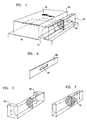
- FIG. 4the laser diode structure and the lens structure are joined (e.g., cemented) to a heat sink 70 wherein a precisely machined ridge 71 serves as a guide for gluing the two structures in precise alignment.
- FIG. 5An alternative approach is presented in FIG. 5 where lens structure 55 is etched at a depth d c of the semiconductor or glass substrate to form two "legs" 56 of precise length (d c ).
- the "legs"permit cementing of the lens structure to the diode structure, such as with epoxy cement. Such cementing does not suffer from the deficiencies of the direct gluing technique of the FIG. 1 structure because the area of strip 10 on facet 25 is not contaminated with glue.
- FIG. 6depicts a spacer 65 (shown in a somewhat reduced scale).
- the spacermay be made of III-V semiconductor material with a hole (66) etched therein to provide the air packet that is necessary for the optical functioning of the lens.
- spacer 65may be cemented to the diode structure and the lens structure.
- the beam emanating from partially reflecting surface 60 of the FIG. 3 structureis substantially circular, but it is still diverging. This beam may be collimated, or even focused with an additional lens that is positioned after surface 60.
- a "post-circularizing" lenscan be created directly on structure 55 by growing a partially reflective coating on surface 60, growing an additional III-V material layer over the partially reflective coating, and etching of a focusing lens 75 therein, as depicted in FIG. 7.
Landscapes
- Physics & Mathematics (AREA)
- General Physics & Mathematics (AREA)
- Optics & Photonics (AREA)
- Condensed Matter Physics & Semiconductors (AREA)
- Electromagnetism (AREA)
- Semiconductor Lasers (AREA)
- Lasers (AREA)
Description
- This invention relates to diode lasers, and more particularly to the construction of wide strip diode lasers.
- A diode laser is commonly created with a GaAs substrate which supports an electrical conductor and which has two parallel faces that are perpendicular to the substrate surface. An epitaxially grown layer of between 1 and 5 quantum wells is grown on the substrate surface and a strip that extends between the two parallel faces is generally created by etching the quantum wells layer. A second epitaxial layer which also supports a second electrical conductor is grown (typically, also GaAs) to cover the quantum wells strip. The two parallel faces are highly polished; with one being partially reflective and the other being either partially or highly reflective.
- When an electrical current is forced through the conductors, the structure lases and light is emitted from the edge of the structure. Specifically, light is emitted from the partially reflective face of the structure in the area that corresponds to the cross section of the quantum wells strip. The light intensity is a function of the current level, but that light cannot be increased without bound by merely raising the current level because when the light is too intense it destroys the epitaxial material and/or the substrate. The overall light power that the diode laser emits can be increased, however, by widening the quantum wells strip.
- The light emitted from a diode laser with a structure as described above does not have a circular cross section. Rather, it corresponds more closely to the shape of the cross section of the quantum wells strip. Consequently, diode lasers that achieve a high optical output through a wider strip possess a light beam that is far from circular. Moreover, the light from such a structure diverges very quickly in the plane perpendicular to the plane of the strip but diverges slowly in the plane of the strip. Thus, the light starts out roughly with a rectangular cross section having the long edge corresponding to the long edge of the strip, and as it travels away from the diode laser it eventually takes on an approximately rectangular cross section with a long edge that is perpendicular to the long edge of the strip.
- At the CLEO ′91 conference in Baltimore, Maryland, May 12-17, 1991, Snyder et al. reported on an approach to arrest the quick divergence of the beam in the perpendicular plane of the diode laser structure described above. "Cylindrical Microlenses for Collimating Laser Diodes", Snyder et al., Conference Proceedings, pp. 28-31. Their proposed structure comprises an optical fiber segment that is attached to the edge of the diode structure in parallel to the strip, as shown in FIG. 1.
Diode laser 5 includes aquantum wells strip 10 spanning a substrate from partiallyreflective facet 20 to highlyreflective facet 30. In FIG. 1, only the cross section ofstrip 10 atsurface 20 is shown. Acylindrical lens 40 that is made of optical fiber is glued to the substrate at the light emitting output area of strip 10 (i.e., at facet 20) and that lens substantially collimates the diverging light in the vertical plane corresponding to the y-axis direction in FIG. 1. It does not collimate the light perpendicular to the diverging light corresponding to the z-axis direction in FIG. 1. - For applications where high intensities and small spot sizes are desired, there are three problems associated with this approach. First, the glue used to attach the lens to the substrate lowers the light intensity at which physical damage to the diode laser begins to show up. That occurs primarily because the glue absorbs light energy that is converted to heat. Second, the lens reduces the divergence rate of the rapidly expanding beam but it does not create a circular beam which may be focused to a small spot size. Third, the wider strip permits multimode operation of the laser and that results in variation in the light intensity along the strip. The latter two problems increase the minimum spot size that can be achieved from the diode laser and, together, the three problems cause the maximumfocused intensity to be decreased.
- An external cavity diode laser according to the invention is defined in
claim 1. - The deficiencies of the prior art are overcome by modifying the partially reflective facet of the laser diode structure to be highly transmissive, by providing a partially reflective facet at a greater distance (thereby lengthening the cavity and reducing the likelihood of high spatial mode operation), and by providing a specifically designed lens.
- More specifically, an improved diode laser is obtained by augmenting the conventional diode laser structure with a cylindrical lens that arrests the divergence of the beam in the spatial direction where it is rapidly diverging. To properly arrest the divergence of the beam and to thereby circularize it, the cylindrical lens is placed at a point in space where the size of the laser beam in the two orthogonal spatial directions is substantially the same. With proper selection of the lens'focal length, the nearly circular cross section of the light is maintained as it travels away from the diode laser.
- The diode laser is further improved by making the diode structure facet that is closest to the lens highly transmissive, and forming a partially reflective facet on the other side of the lens. This elongates the resonance cavity.
- In one embodiment, for example, the lens is constructed by etching a refractive convex lens on a glass (or III-V semiconductor) substrate and positioning the lens substrate so that the back surface of the substrate forms the partially reflective facet that is needed to sustain lasing. Proper positioning of the lens with respect to the lasing structure is accomplished by appropriately recessing the lens.
- FIG. 1 illustrates a prior art construction of a laser diode and a post-emission cylindrical lens for collimating the light output;
- FIG. 2 presents a plot of beam divergence rates as a function of beam size;
- FIG. 3 depicts a laser diode construction in accord with the principles of this invention;
- FIG. 4 illustrates one means for accurately positioning cylindrical lens/mirror structure relative to the lasing structure;
- FIG. 5 depicts one approach for integrating both the lens and the positioning means;
- FIG. 6 presents another means for accurately positioning cylindrical lens/mirror structure relative to the lasing structure; and
- FIG. 7 shows an approach for including a collimating/focusing lens.
- It is well known that a light source with a small aperture diverges more quickly than a light source with a larger aperture. See, for example, "Solid State Laser Engineering", W. Koechner, Springer-Verlag, 1976,
Section 5. 1.2, pp. 176-178. This is illustrated diagrammatically in FIG. 2 whereplot 11 depicts the divergence of the light beam from a narrow light source, andplot 12 depicts the divergence of the light beam from a wider light source. As indicated above, the primary technique for increasing the power capability of a laser diode is to create a wider strip. However, that only increases the difference between the size of the light source when viewed in the two orthogonal directions that correspond to the width of the strip and the thickness of the strip (z-axis and y-axis directions, respectively). Regardless of the width of the strip, however, as can be seen from FIG. 2 there is always a distance, dc, where the girth of the quickly diverging beam is equal to the girth of the slowly diverging beam. An image obtained at the distance dc is substantially circular. - The circular cross section of the beam can be maintained from distance dc onward if the divergence of the beam in the two directions can be equalized. That is accomplished, in accordance with this invention, by placing an elongated lens at location dc. The placed lens reduces the rate of beam divergence in the plane where it diverges quickly, i.e., in the y-axis direction, to match the divergence rate in the z-axis direction. An arrangement that accomplishes this desired effect is depicted in FIG. 3, where a lens is placed at distance dc away from the facet of the diode laser structure that emits light. The lens is a columnar lens which partially collimates light only in the y direction. More specifically, the FIG. 3 lens is column-like, with a column cross section that is perpendicular to an axis of the column (that is also parallel to the z axis in FIG. 3), and that cross section is shaped to arrest the divergence of the beam in the y axis. In the FIG. 3 lens, this cross section has a curved surface (as pointed to by numeral 55), which gives a convex columnar surface to the lens.
- The divergence of Gaussian beams can be theoretically described through the use of Gaussian Beam Propagation equations (see above-cited reference). By using the Gaussian Beam Propagation equations, one can determine the focal length of a columnar lens which equalizes the beam divergence in both the x and y dimensions. Once the beam size and the beam divergence are equalized in both dimensions, the output beam remains circular at all subsequent distances. By "focal length" what is meant is the distance from a point source to a plane in the columnar lens (in the y-z plane), known as the principla plane, which causes the light of the point source to collimate along the y axis. In FIG. 3, the demarcation of distance dc indicates that the principal plane is approximately the plane that separates the convex portion of the lens from the rectangular portion of the lens.
- FIG. 3 illustrates a structure that is similar to the FIG. 1 diode laser structure but which embodies the principles disclosed herein. It includes a broad strip
quantum wells layer 10, afacet 25 and afacet 35. Facet 35 (hidden from view) is perpendicular to the plane ofstrip 10 and preferably is highly reflective. Acolumnar lens structure 55 is positioned at a distance dc away fromfacet 25, with the long axis of the lens being parallel tofacet 25 and to the plane ofstrip 10. Unlikelens 40 in the FIG. 1 drawing, the curved surface instructure 55 that makes up lensfacessurface 25.Lens structure 55 also includes asurface 60 that is parallel tofacet 35. In accordance with another aspect of the improved laser diode,surface 60 is partially reflective, while both surface 25 and the curved surface of the lens are highly transmissive. - The reason for making
facet 25 highly transmissive relates to the fact that the broad strip structure permits high spatial mode operation of the laser diode. The light bouncing between the parallel facets of the diode structure can bounce at off-normal angles, and that causes the light intensity profile to be non-uniform along the z-axis direction. The non-uniform intensity profile is improved by lengthening the laser cavity, which in the FIG. 3 embodiment is accomplished by makingsurface 60 rather thanfacet 25 highlytransmissive Facet 25 and the curved surface of the lens are made highly transmissive by applying an anti-reflective coating to the surfaces in a conventional manner. Of course, to make the entire arrangement lase,surface 60 needs to be positioned parallel tofacet 35. - For the FIG. 3 embodiment,
lens structure 55 can be created by etching a III-V semiconductor or glass substrate to form a lens as described, for example, in a application by G. Derkits, EP-A-0458514 titled "Partially or Fully Recessed Microlens Fabrication" and falling within the terms of Article 54(3) EPC.Lens 55 may be diffractive, a Fresnel lens, or a refractive lens as shown in FIG. 3. The latter is most efficient in performing the intended function. - From the above it may be appreciated that positioning of
structure 55 with respect to strip 10 andfacet 35 must be precise in two respects.Surface 60 must be parallel tofacet 35 and the lens must be at distance dc fromfacet 25. There are numerous ways to effectuate this positioning. In FIG. 4, the laser diode structure and the lens structure are joined (e.g., cemented) to a heat sink 70 wherein a precisely machinedridge 71 serves as a guide for gluing the two structures in precise alignment. An alternative approach is presented in FIG. 5 wherelens structure 55 is etched at a depth dc of the semiconductor or glass substrate to form two "legs" 56 of precise length (dc). The "legs" permit cementing of the lens structure to the diode structure, such as with epoxy cement. Such cementing does not suffer from the deficiencies of the direct gluing technique of the FIG. 1 structure because the area ofstrip 10 onfacet 25 is not contaminated with glue. - Still another approach is presented by FIG. 6 which depicts a spacer 65 (shown in a somewhat reduced scale). The spacer may be made of III-V semiconductor material with a hole (66) etched therein to provide the air packet that is necessary for the optical functioning of the lens. Again,
spacer 65 may be cemented to the diode structure and the lens structure. - The beam emanating from partially reflecting
surface 60 of the FIG. 3 structure is substantially circular, but it is still diverging. This beam may be collimated, or even focused with an additional lens that is positioned aftersurface 60. Alternatively, a "post-circularizing" lens can be created directly onstructure 55 by growing a partially reflective coating onsurface 60, growing an additional III-V material layer over the partially reflective coating, and etching of a focusinglens 75 therein, as depicted in FIG. 7.
Claims (10)
- An external cavity diode laser having a broad quantum wells strip (10) between a first facet (35), which is at least partially reflective, and a second facet (25) parallel to said first facet, which strip appears at the second facet with a cross section having a long measure along a first axis and a short measure along a second axis that is perpendicular to the first axis, and a columnar cylindrical lens (55) with a long dimension along a longitudinal axis and a cross section perpendicular to the longitudinal axis that arrests divergence of light along said second axis, situated in proximity to said second facet with its longitudinal axis parallel to said first axis, wherein:
said second facet is highly transmissive,
the longitudinal center of the cylindrical lens lies parallel to said first axis and is situated approximately at a distance dc from said second facet, with dc being the distance from said second facet where the girth of a light beam emanating from said optically emitting area is substantially the same in the direction of said first axis and said second axis, and
a third facet (60) is included following said cylindrical lens which is parallel to said first facet and is at least partially reflective. - The diode laser of claim 1 where a light beam emanating from the cross section of the strip at the second facet diverges as it travels toward said lens and the focal length of said lens is set to equalize the rate of divergence of said light beam in the direction of said long edge and in a direction perpendicular to said long edge.
- The diode laser of claim 1 further including a partially reflective layer associated with said third facet and a focusing lens (75) following said third facet.
- The laser of claim 1 comprising an anti-reflective coating over said columnar lens.
- The laser of claim 1 wherein said columnar lens is a refractive lens.
- The laser of claim 1 wherein said columnar lens is a diffractive lens.
- The laser of claim 1 wherein a physical spacer (65) is situated between said highly transmissive facet and said laser structure.
- The laser of claim 1 where the columnar lens is fabricated on one surface of a transmissive substrate and said third facet is fabricated on another surface of said transmissive substrate.
- The laser of claim 8 wherein said transmissive substrate includes a protrusion (56) tailored to said distance.
- The laser of claim 8 further including a base element (70) with positioning means (71) to affix said diode structure and said transmissive substrate structure in alignment with each other.
Applications Claiming Priority (2)
| Application Number | Priority Date | Filing Date | Title |
|---|---|---|---|
| US07/774,929US5206878A (en) | 1991-10-11 | 1991-10-11 | Wide strip diode laser employing a lens |
| US774929 | 1991-10-11 |
Publications (2)
| Publication Number | Publication Date |
|---|---|
| EP0536945A1 EP0536945A1 (en) | 1993-04-14 |
| EP0536945B1true EP0536945B1 (en) | 1995-08-16 |
Family
ID=25102730
Family Applications (1)
| Application Number | Title | Priority Date | Filing Date |
|---|---|---|---|
| EP92308944AExpired - LifetimeEP0536945B1 (en) | 1991-10-11 | 1992-10-01 | A wide strip diode laser employing a lens |
Country Status (5)
| Country | Link |
|---|---|
| US (1) | US5206878A (en) |
| EP (1) | EP0536945B1 (en) |
| JP (1) | JP2542777B2 (en) |
| CA (1) | CA2079504C (en) |
| DE (1) | DE69204135T2 (en) |
Families Citing this family (17)
| Publication number | Priority date | Publication date | Assignee | Title |
|---|---|---|---|---|
| US20030043463A1 (en)* | 1992-03-30 | 2003-03-06 | Yajun Li | Athermalized plastic lens |
| US6092728A (en)* | 1992-03-30 | 2000-07-25 | Symbol Technologies, Inc. | Miniature laser diode focusing module using micro-optics |
| US5307430A (en)* | 1992-11-30 | 1994-04-26 | The United States Of America As Represented By The United States Department Of Energy | Lensing duct |
| US5581414A (en)* | 1993-02-22 | 1996-12-03 | Blue Sky Research Incorporated | Microlens assemblies and couplers |
| US5343546A (en)* | 1993-03-26 | 1994-08-30 | Polaroid Corporation | Microbench |
| JPH07115244A (en)* | 1993-10-19 | 1995-05-02 | Toyota Motor Corp | Semiconductor laser and manufacturing method thereof |
| US5566267A (en)* | 1994-12-15 | 1996-10-15 | Ceram Optec Industries Inc. | Flat surfaced optical fibers and diode laser medical delivery devices |
| DE19706276B4 (en)* | 1997-02-18 | 2011-01-13 | Siemens Ag | A semiconductor laser device and method of manufacturing a semiconductor laser device |
| US6868099B1 (en) | 1999-11-04 | 2005-03-15 | Wisconsin Alumni Research Foundation | Frequency-narrowed high power diode laser system with external cavity |
| US6584133B1 (en) | 2000-11-03 | 2003-06-24 | Wisconsin Alumni Research Foundation | Frequency-narrowed high power diode laser array method and system |
| JP2002232056A (en)* | 2001-01-31 | 2002-08-16 | Hamamatsu Photonics Kk | Semiconductor laser device, and fastening method of lens position thereof |
| JP4567213B2 (en)* | 2001-01-31 | 2010-10-20 | 浜松ホトニクス株式会社 | Semiconductor laser device and lens position fixing method of semiconductor laser device |
| JP2002314188A (en)* | 2001-04-13 | 2002-10-25 | Hamamatsu Photonics Kk | Semiconductor laser device |
| JP4951691B2 (en)* | 2010-04-13 | 2012-06-13 | 株式会社日立製作所 | Optical transmission module and optical communication device using the same |
| DE102012215684A1 (en)* | 2012-09-04 | 2014-03-06 | Osram Opto Semiconductors Gmbh | Method for manufacturing laser component i.e. laser package, for surface mounting technology assembly, involves positioning laser chip on supporting substrate, where side surface of laser chip is attached with stop element |
| DE102013216525A1 (en)* | 2013-08-21 | 2015-02-26 | Osram Opto Semiconductors Gmbh | Laser component and method for producing a laser component |
| DE102017123798B4 (en)* | 2017-10-12 | 2022-03-03 | OSRAM Opto Semiconductors Gesellschaft mit beschränkter Haftung | Semiconductor lasers and manufacturing processes for optoelectronic semiconductor components |
Family Cites Families (11)
| Publication number | Priority date | Publication date | Assignee | Title |
|---|---|---|---|---|
| JPS52131969U (en)* | 1976-04-01 | 1977-10-06 | ||
| JPS5545239U (en)* | 1978-09-18 | 1980-03-25 | ||
| GB2046005B (en)* | 1979-03-29 | 1983-02-09 | Standard Telephones Cables Ltd | Injection laser devices |
| JPS6043680B2 (en)* | 1979-09-21 | 1985-09-30 | 日本電信電話株式会社 | Temperature stabilized laser device |
| JPS60258993A (en)* | 1984-06-06 | 1985-12-20 | Hitachi Ltd | semiconductor light emitting device |
| JPS61258487A (en)* | 1985-05-11 | 1986-11-15 | Fujitsu Ltd | Manufacturing method of quantum well laser |
| JPH02216881A (en)* | 1989-02-17 | 1990-08-29 | Canon Inc | External resonant semiconductor laser device |
| US5027359A (en)* | 1989-10-30 | 1991-06-25 | Massachusetts Institute Of Technology | Miniature Talbot cavity for lateral mode control of laser array |
| US4995050A (en)* | 1989-11-17 | 1991-02-19 | Spectra Diode Laboratories, Inc. | Diode laser with external lens cavity |
| EP0429243A3 (en)* | 1989-11-17 | 1991-12-27 | Minnesota Mining And Manufacturing Company | Beam shaping system using diffraction |
| US5081639A (en)* | 1990-10-01 | 1992-01-14 | The United States Of America As Represented By The United States Department Of Energy | Laser diode assembly including a cylindrical lens |
- 1991
- 1991-10-11USUS07/774,929patent/US5206878A/ennot_activeExpired - Lifetime
- 1992
- 1992-09-30CACA002079504Apatent/CA2079504C/ennot_activeExpired - Fee Related
- 1992-10-01EPEP92308944Apatent/EP0536945B1/ennot_activeExpired - Lifetime
- 1992-10-01DEDE69204135Tpatent/DE69204135T2/ennot_activeExpired - Fee Related
- 1992-10-08JPJP4293987Apatent/JP2542777B2/ennot_activeExpired - Fee Related
Also Published As
| Publication number | Publication date |
|---|---|
| DE69204135D1 (en) | 1995-09-21 |
| CA2079504C (en) | 1997-10-14 |
| US5206878A (en) | 1993-04-27 |
| JPH05206578A (en) | 1993-08-13 |
| JP2542777B2 (en) | 1996-10-09 |
| DE69204135T2 (en) | 1996-04-25 |
| EP0536945A1 (en) | 1993-04-14 |
| CA2079504A1 (en) | 1993-04-12 |
Similar Documents
| Publication | Publication Date | Title |
|---|---|---|
| EP0536945B1 (en) | A wide strip diode laser employing a lens | |
| US4785459A (en) | High efficiency mode matched solid state laser with transverse pumping | |
| US4803696A (en) | Laser with grating feedback unstable resonator | |
| US4908832A (en) | High efficiency mode-matched solid-state laser with transverse pumping | |
| US5485482A (en) | Method for design and construction of efficient, fundamental transverse mode selected, diode pumped, solid state lasers | |
| US7965910B2 (en) | Beam combination using interleaved optical plates | |
| US6259713B1 (en) | Laser beam coupler, shaper and collimator device | |
| US4894839A (en) | High efficiency mode-matched solid-state laser with transverse pumping | |
| US5181223A (en) | High-efficiency mode-matched transversely-pumped solid state laser amplifier | |
| US4530574A (en) | Beam collimation and focusing of multi-emitter or broad emitter lasers | |
| EP3696925A1 (en) | Semiconductor laser | |
| AU5555890A (en) | External cavity semiconductor laser | |
| US6125222A (en) | Fiber grating feedback stabilization of broad area laser diode | |
| WO2016080252A1 (en) | External resonator-type semiconductor laser | |
| EP0100242B1 (en) | Optical system for a laser | |
| JP2006339638A (en) | A surface emitting laser coupled with a pump laser on a single heat sink. | |
| TWI244815B (en) | Optically pumped semiconductor laser device | |
| US5757830A (en) | Compact micro-optical edge-emitting semiconductor laser assembly | |
| US20080025353A1 (en) | Wavelength locked diode-laser bar | |
| US3875532A (en) | Semiconductor laser device having a light focusing transmission | |
| Chen et al. | Collimating diode laser beams from a large-area VCSEL-array using microlens array | |
| US7010012B2 (en) | Method and apparatus for reducing specular reflections in semiconductor lasers | |
| US4797892A (en) | Longitudinally coupled surface emitting semiconductor laser array | |
| Reitterer et al. | Integrated RGB laser light module for autostereoscopic outdoor displays | |
| Larat et al. | 11-W CW 100-µm fiber-coupled 971-nm Al-free active region pump source |
Legal Events
| Date | Code | Title | Description |
|---|---|---|---|
| PUAI | Public reference made under article 153(3) epc to a published international application that has entered the european phase | Free format text:ORIGINAL CODE: 0009012 | |
| AK | Designated contracting states | Kind code of ref document:A1 Designated state(s):DE FR GB | |
| 17P | Request for examination filed | Effective date:19931001 | |
| 17Q | First examination report despatched | Effective date:19940223 | |
| RAP3 | Party data changed (applicant data changed or rights of an application transferred) | Owner name:AT&T CORP. | |
| GRAA | (expected) grant | Free format text:ORIGINAL CODE: 0009210 | |
| AK | Designated contracting states | Kind code of ref document:B1 Designated state(s):DE FR GB | |
| REF | Corresponds to: | Ref document number:69204135 Country of ref document:DE Date of ref document:19950921 | |
| ET | Fr: translation filed | ||
| PLBE | No opposition filed within time limit | Free format text:ORIGINAL CODE: 0009261 | |
| 26N | No opposition filed | ||
| PGFP | Annual fee paid to national office [announced via postgrant information from national office to epo] | Ref country code:FR Payment date:19990923 Year of fee payment:8 | |
| PGFP | Annual fee paid to national office [announced via postgrant information from national office to epo] | Ref country code:GB Payment date:19990928 Year of fee payment:8 | |
| PGFP | Annual fee paid to national office [announced via postgrant information from national office to epo] | Ref country code:DE Payment date:19991231 Year of fee payment:8 | |
| PG25 | Lapsed in a contracting state [announced via postgrant information from national office to epo] | Ref country code:GB Free format text:LAPSE BECAUSE OF NON-PAYMENT OF DUE FEES Effective date:20001001 | |
| GBPC | Gb: european patent ceased through non-payment of renewal fee | Effective date:20001001 | |
| PG25 | Lapsed in a contracting state [announced via postgrant information from national office to epo] | Ref country code:FR Free format text:LAPSE BECAUSE OF NON-PAYMENT OF DUE FEES Effective date:20010629 | |
| PG25 | Lapsed in a contracting state [announced via postgrant information from national office to epo] | Ref country code:DE Free format text:LAPSE BECAUSE OF NON-PAYMENT OF DUE FEES Effective date:20010703 | |
| REG | Reference to a national code | Ref country code:FR Ref legal event code:ST |