EP0532592B1 - Chrominance processing and timing system - Google Patents
Chrominance processing and timing systemDownload PDFInfo
- Publication number
- EP0532592B1 EP0532592B1EP91910788AEP91910788AEP0532592B1EP 0532592 B1EP0532592 B1EP 0532592B1EP 91910788 AEP91910788 AEP 91910788AEP 91910788 AEP91910788 AEP 91910788AEP 0532592 B1EP0532592 B1EP 0532592B1
- Authority
- EP
- European Patent Office
- Prior art keywords
- data
- signal
- video
- picture
- display
- Prior art date
- Legal status (The legal status is an assumption and is not a legal conclusion. Google has not performed a legal analysis and makes no representation as to the accuracy of the status listed.)
- Expired - Lifetime
Links
Images


Classifications
- H—ELECTRICITY
- H04—ELECTRIC COMMUNICATION TECHNIQUE
- H04N—PICTORIAL COMMUNICATION, e.g. TELEVISION
- H04N9/00—Details of colour television systems
- H04N9/64—Circuits for processing colour signals
- H04N9/641—Multi-purpose receivers, e.g. for auxiliary information
- G—PHYSICS
- G06—COMPUTING OR CALCULATING; COUNTING
- G06T—IMAGE DATA PROCESSING OR GENERATION, IN GENERAL
- G06T3/00—Geometric image transformations in the plane of the image
- G06T3/04—Context-preserving transformations, e.g. by using an importance map
- G—PHYSICS
- G06—COMPUTING OR CALCULATING; COUNTING
- G06T—IMAGE DATA PROCESSING OR GENERATION, IN GENERAL
- G06T3/00—Geometric image transformations in the plane of the image
- G06T3/40—Scaling of whole images or parts thereof, e.g. expanding or contracting
- G06T3/4007—Scaling of whole images or parts thereof, e.g. expanding or contracting based on interpolation, e.g. bilinear interpolation
- H—ELECTRICITY
- H04—ELECTRIC COMMUNICATION TECHNIQUE
- H04N—PICTORIAL COMMUNICATION, e.g. TELEVISION
- H04N19/00—Methods or arrangements for coding, decoding, compressing or decompressing digital video signals
- H04N19/90—Methods or arrangements for coding, decoding, compressing or decompressing digital video signals using coding techniques not provided for in groups H04N19/10-H04N19/85, e.g. fractals
- H—ELECTRICITY
- H04—ELECTRIC COMMUNICATION TECHNIQUE
- H04N—PICTORIAL COMMUNICATION, e.g. TELEVISION
- H04N3/00—Scanning details of television systems; Combination thereof with generation of supply voltages
- H04N3/10—Scanning details of television systems; Combination thereof with generation of supply voltages by means not exclusively optical-mechanical
- H04N3/16—Scanning details of television systems; Combination thereof with generation of supply voltages by means not exclusively optical-mechanical by deflecting electron beam in cathode-ray tube, e.g. scanning corrections
- H04N3/22—Circuits for controlling dimensions, shape or centering of picture on screen
- H04N3/223—Controlling dimensions
- H—ELECTRICITY
- H04—ELECTRIC COMMUNICATION TECHNIQUE
- H04N—PICTORIAL COMMUNICATION, e.g. TELEVISION
- H04N3/00—Scanning details of television systems; Combination thereof with generation of supply voltages
- H04N3/10—Scanning details of television systems; Combination thereof with generation of supply voltages by means not exclusively optical-mechanical
- H04N3/16—Scanning details of television systems; Combination thereof with generation of supply voltages by means not exclusively optical-mechanical by deflecting electron beam in cathode-ray tube, e.g. scanning corrections
- H04N3/22—Circuits for controlling dimensions, shape or centering of picture on screen
- H04N3/227—Centering
- H—ELECTRICITY
- H04—ELECTRIC COMMUNICATION TECHNIQUE
- H04N—PICTORIAL COMMUNICATION, e.g. TELEVISION
- H04N3/00—Scanning details of television systems; Combination thereof with generation of supply voltages
- H04N3/10—Scanning details of television systems; Combination thereof with generation of supply voltages by means not exclusively optical-mechanical
- H04N3/16—Scanning details of television systems; Combination thereof with generation of supply voltages by means not exclusively optical-mechanical by deflecting electron beam in cathode-ray tube, e.g. scanning corrections
- H04N3/27—Circuits special to multi-standard receivers
- H—ELECTRICITY
- H04—ELECTRIC COMMUNICATION TECHNIQUE
- H04N—PICTORIAL COMMUNICATION, e.g. TELEVISION
- H04N5/00—Details of television systems
- H04N5/222—Studio circuitry; Studio devices; Studio equipment
- H04N5/262—Studio circuits, e.g. for mixing, switching-over, change of character of image, other special effects ; Cameras specially adapted for the electronic generation of special effects
- H04N5/2624—Studio circuits, e.g. for mixing, switching-over, change of character of image, other special effects ; Cameras specially adapted for the electronic generation of special effects for obtaining an image which is composed of whole input images, e.g. splitscreen
- H—ELECTRICITY
- H04—ELECTRIC COMMUNICATION TECHNIQUE
- H04N—PICTORIAL COMMUNICATION, e.g. TELEVISION
- H04N5/00—Details of television systems
- H04N5/44—Receiver circuitry for the reception of television signals according to analogue transmission standards
- H04N5/445—Receiver circuitry for the reception of television signals according to analogue transmission standards for displaying additional information
- H04N5/45—Picture in picture, e.g. displaying simultaneously another television channel in a region of the screen
- H—ELECTRICITY
- H04—ELECTRIC COMMUNICATION TECHNIQUE
- H04N—PICTORIAL COMMUNICATION, e.g. TELEVISION
- H04N7/00—Television systems
- H04N7/007—Systems with supplementary picture signal insertion during a portion of the active part of a television signal, e.g. during top and bottom lines in a HDTV letter-box system
- H—ELECTRICITY
- H04—ELECTRIC COMMUNICATION TECHNIQUE
- H04N—PICTORIAL COMMUNICATION, e.g. TELEVISION
- H04N7/00—Television systems
- H04N7/01—Conversion of standards, e.g. involving analogue television standards or digital television standards processed at pixel level
- H—ELECTRICITY
- H04—ELECTRIC COMMUNICATION TECHNIQUE
- H04N—PICTORIAL COMMUNICATION, e.g. TELEVISION
- H04N7/00—Television systems
- H04N7/01—Conversion of standards, e.g. involving analogue television standards or digital television standards processed at pixel level
- H04N7/0105—Conversion of standards, e.g. involving analogue television standards or digital television standards processed at pixel level using a storage device with different write and read speed
- H—ELECTRICITY
- H04—ELECTRIC COMMUNICATION TECHNIQUE
- H04N—PICTORIAL COMMUNICATION, e.g. TELEVISION
- H04N7/00—Television systems
- H04N7/01—Conversion of standards, e.g. involving analogue television standards or digital television standards processed at pixel level
- H04N7/0117—Conversion of standards, e.g. involving analogue television standards or digital television standards processed at pixel level involving conversion of the spatial resolution of the incoming video signal
- H04N7/0122—Conversion of standards, e.g. involving analogue television standards or digital television standards processed at pixel level involving conversion of the spatial resolution of the incoming video signal the input and the output signals having different aspect ratios
- H—ELECTRICITY
- H04—ELECTRIC COMMUNICATION TECHNIQUE
- H04N—PICTORIAL COMMUNICATION, e.g. TELEVISION
- H04N7/00—Television systems
- H04N7/015—High-definition television systems
- H—ELECTRICITY
- H04—ELECTRIC COMMUNICATION TECHNIQUE
- H04N—PICTORIAL COMMUNICATION, e.g. TELEVISION
- H04N9/00—Details of colour television systems
- H04N9/64—Circuits for processing colour signals
Definitions
- the inventionrelates to the field of televisions, for example those televisions having a wide display format ratio screen, which must interpolate video data to implement various display formats.
- Most televisions todayhave a format display ratio, horizontal width to vertical height, of 4:3.
- a wide format display ratiocorresponds more closely to the display format ratio of movies, for example 16:9.
- the inventionis applicable to both direct view televisions and projection televisions.
- Televisions having a format display ratio of 4:3, often referred to as 4 X 3are limited in the ways that single and multiple video signal sources can be displayed.
- Television signal transmissions of commercial broadcasters, except for experimental material,are broadcast with a 4X3 format display ratio.
- Many viewersfind the 4 X 3 display format less pleasing than the wider format display ratio associated with the movies.
- Televisions with a wide format display ratioprovide not only a more pleasing display, but are capable of displaying wide display format signal sources in a corresponding wide display format. Movies "look" like movies, not cropped or distorted versions thereof.
- the video sourceneed not be cropped, either when converted from film to video, for example with a telecine device, or by processors in the television.
- a wide screen television according to various inventive arrangementsis capable of providing high resolution, single and multiple picture displays, from single and multiple sources having similar or different format ratios, and with selectable display format ratios.
- Televisions with a wide display format ratiocan be implemented in television systems displaying video signals both at basic or standard horizontal scanning rates and multiples thereof, as well as by both interlaced and noninterlaced scanning.
- Standard NTSC video signalsfor example, are displayed by interlacing the successive fields of each video frame, each field being generated by a raster scanning operation at a basic or standard horizontal scanning rate of approximately 15,734 Hz.
- the basic scanning rate for video signalsis variously referred to as f H , 1f H , and 1H.
- the actual frequency of a 1f H signalwill vary according to different video standards.
- systemshave been developed for displaying video signals progressively, in a noninterlaced fashion.
- Progressive scanningrequires that each displayed frame must be scanned in the same time period allotted for scanning one of the two fields of the interlaced format.
- Flicker free AA-BB displaysrequire that each field be scanned twice, consecutively.
- the horizontal scanning frequencymust be twice that of the standard horizontal frequency.
- the scanning rate for such progressively scanned or flicker free displaysis variously referred to as 2f H and 2H.
- a 2f H scanning frequency according to standards in the United States, for example,is approximately 31,468 Hz.
- the video datamust be selectively compressed and expanded, depending upon the desired format. In one case, for example, it is necessary to compress the 4 X 3 NTSC video by a factor of 4/3 to avoid aspect ratio distortion of the displayed picture. In the other case, for example, the video can be expanded to perform horizontal zooming operations usually accompanied by vertical zooming. Horizontal zoom operations up to 33% can be accomplished by reducing compressions to less than 4/3.
- a sample interpolatoris used to recalculate the incoming video to a new pixel positions because the luminance video bandwidth, up to 5.5 MHz for S-VHS format, occupies a large percentage of the Nyquist or fold over frequency, which is 8 MHz for a 1024f H system clock.
- EP-A-0 162 501discloses a video signal processing arrangement having one memory and one interpolator for processing luminance data, and one memory and one interpolator for processing chrominance data.
- a control circuitproduces control signals to reconfigure the positions of the memory and the interpolator depending on whether the video signal is to be compressed or expanded.
- GB-A-2 073 536discloses a video signal processing circuit for expanding or compressing a color television signal in the horizontal direction.
- Each of the three video signal paths corresponding to the Y, U, and V signal components of a color television signalinclude a memory, an interpolator and an output selector. Input signals are stored in memory.
- a read address generatorcontrols reading from memory and controls the appropriate interpolator to provide the desired interpolation.
- the luminance data for the main signalis routed along a main signal path including a FIFO line memory for compressing (pausing) and expanding (repeating) the data and an interpolator for recalculating sample values to smooth the data.
- a main signal pathincluding a FIFO line memory for compressing (pausing) and expanding (repeating) the data and an interpolator for recalculating sample values to smooth the data.
- switches or route selectorsreverse the topology of the main signal path with respect to the relative positions of the FIFO and the interpolator, avoiding the need for two main signal paths requiring two FIFOs and two interpolators.
- these switchesselect whether the interpolator precedes the FIFO, as required for compression, or whether the FIFO precedes the interpolator, as required for expansion.
- the switchescan be responsive to a route control circuit which is itself responsive to a microprocessor.
- An interpolator control circuitgenerates pixel position values, interpolator compensation filter weighting and clock gating information for the luminance data. It is the clock gating information which pauses (decimates) or repeats the FIFO data to allow samples not to be written on some clocks for effecting compression or some samples to be read multiple times for expansion.
- clock gating informationwhich pauses (decimates) or repeats the FIFO data to allow samples not to be written on some clocks for effecting compression or some samples to be read multiple times for expansion.
- every fourth samplecan be inhibited from being written into the FIFO.
- the average slope of a ramp read out of the luminance FIFOis 33% steeper than the corresponding input ramp. Note also that 33% less active reading time is required to read out the ramp as was required to write in the data. This constitutes the 4 / 3 compression. It is the function of the interpolator to recalculate the luminance samples being written into the FIFO so that the data read out of the FIFO is smooth,
- Expansionsmay be performed in exactly the opposite manner as compressions.
- the write enable signalhas clock gating information attached to it in the form of inhibit pulses.
- the clock gating informationis applied to the read enable signal. This will pause the data as it is being read from the FIFO.
- the average slope of a ramp read out of the luminance FIFOis 33% more shallow than the corresponding input ramp for a 4 / 3 expansion or zoom.
- itis the function of the interpolator, which follows the FIFO, to recalculate the sampled data from jagged to smooth after the expansion.
- the datamust pause while being read from the FIFO and while being clocked into the interpolator.
- the clock gating operationsmay be performed in a synchronous manner. If a switchable video data path topology were not used to interchange the positions of the interpolator and FIFO, the read or write clocks would need to be double clocked to pause or repeat the data.
- double clockedmeans that two data points must be written into the FIFO in a single clock cycle or read from the FIFO during a single clock cycle. The resulting circuitry cannot be made to operate synchronously with the system clock, since the writing or reading clock frequency must be twice as high as the system clock frequency.
- the switchable topologyrequires only one interpolator and one FIFO to perform both compressions and expansions. If the video path switching arrangement described herein were not used, the double clocking situation can be avoided only by using two FIFO's to accomplish both compression and expansion. One FIFO for expansions would need to be placed in front of the interpolator and one FIFO for compressions would need to be placed after the interpolator.
- a circuit for compressing and expanding video color component datacomprises a FIFO line memory and a delay matching circuit.
- a timing circuitgenerates control signals for writing data into the line memory and for reading data from the line memory to compress and expand the data.
- the delay matching circuitmatches the data, compressed or expanded in the FIFO line memory, to luminance data which is similarly compressed or expanded.
- a switching networkselectively establishes a first signal path in which the line memory precedes the delay matching circuit for implementing the data expansion and a second signal path in which the delay matching circuit precedes the line memory for implementing the data compression.
- the switching networkis controlled according to selected display formats requiring compression or expansion, for example by a microprocessor.
- FIGURES 1(a)-1(i)are useful for explaining different display formats of a wide screen television.
- FIGURE 2is a block diagram of a wide screen television in accordance with aspects of this invention and adapted for operation at 2fH horizontal scanning.
- FIGURES 3is a block diagram of the wide screen processor shown in FIGURE 2.
- FIGURE 4is a block diagram showing further details of the wide screen processor shown in FIGURE 3.
- FIGURE 5is a block diagram of the picture-in-picture processor shown in FIGURE 4.
- FIGURE 6is a block diagram of the gate array shown in FIGURE 4 and illustrating the main, auxiliary and output signal paths.
- FIGURES 7 and 8are timing diagrams useful for explaining the generation of the display format shown in FIGURE 1(d), using fully cropped signals.
- FIGURE 9is a block diagram showing the main signal path of FIGURE 6 in more detail.
- FIGURE 10is a block diagram showing the auxiliary signal path of FIGURE 6 in more detail.
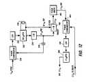
- FIGURE 11is a block diagram of the timing and control section of the picture-in-picture processor of FIGURE 5.
- FIGURE 12is a block diagram of a circuit for generating the internal 2f H signal in the 1f H to 2f H conversion.
- FIGURE 13is a combination block and circuit diagram for the deflection circuit shown in FIGURE 2.
- FIGURE 14is a block diagram of the RGB interface shown in FIGURE 2.
- FIGURES 15(a)-15(f)illustrate waveforms useful for explaining the analog to digital conversion of the color components of the main video signal.
- FIGURE 16is a block diagram of an alternative topology in the gate array for the signal processing path of the color components of the main video signal.
- FIGURES 17(a)-17(b)illustrate waveforms useful for explaining skewing of luminance and color components in the main signal path of the gate array.
- FIGURE 1illustrate some, but not all of the various combinations of single and multiple picture display formats which can be implemented according to different inventive arrangements. Those selected for illustration are intended to facilitate the description of particular circuits comprising wide screen televisions according to the inventive arrangements.
- the inventive arrangementsare in some cases directed to the display formats themselves, apart from specific underlying circuitry. For purposes of convenience in illustration and discussion herein, a conventional display format ratio of width to height for a video source or signal is generally deemed to be 4 X 3, whereas a wide screen display format ratio of width to height for a video source or signal is generally deemed to be 16 X 9.
- inventive arrangementsare not limited by these definitions.
- FIGURE 1(a)illustrates a television, direct view or projection, having a conventional format display ratio of 4X3.
- a 16 X 9 format display ratio pictureis transmitted, as a 4X3 format display ratio signal, black bars appear at the top and at the bottom.
- Thisis commonly referred to as letterbox format.
- the viewed pictureis rather small with respect to the entire available display area.
- the 16 X 9 format display ratio sourceis converted prior to transmission, so that it will fill the vertical extent of a viewing surface of 4X3 format display. However, much information will be cropped from the left and/or right sides.
- the letterbox picturecan be expanded vertically but not horizontally, whereby the resulting picture will evidence distortion by vertical elongation. None of the three alternatives is particularly appealing.
- FIGURE 1(b)shows a 16 X 9 screen.
- a 16 X 9 format display ratio video sourcewould be fully displayed, without cropping and without distortion.
- a 16 X 9 format display ratio letterbox picturewhich is itself in a 4X3 format display ratio signal, can be progressively scanned by line doubling or line addition, so as to provide a larger display with sufficient vertical resolution.
- a wide screen television in accordance with this inventioncan display such a 16 X 9 format display ratio signal whether the main source, the auxiliary source or an external RGB source.
- FIGURE 1(c)illustrates a 16 X 9 format display ratio main signal in which a 4X3 format display ratio inset picture is displayed. If both the main and auxiliary video signals are 16 X 9 format display ratio sources, the inset picture can also have a 16 X 9 format display ratio. The inset picture can be displayed in many different positions.
- FIGURE 1(d)illustrates a display format, wherein the main and auxiliary video signals are displayed with the same size picture.
- Each display areahas an format display ratio of 8 X 9, which is of course different from both 16 X 9 and 4 X 3.
- the signalIn order to show a 4X3 format display ratio source in such a display area, without horizontal or vertical distortion, the signal must be cropped on the left and/or right sides. More of the picture can be shown, with less cropping, if some aspect ratio distortion by horizontal squeezing of the picture is tolerated. Horizontal squeezing results in vertical elongation of objects in the picture.
- the wide screen television according to this inventioncan provide any mix of cropping and aspect ratio distortion from maximum cropping with no aspect ratio distortion to no cropping with maximum aspect ratio distortion.
- FIGURE 1(e)is a display format wherein a 4 X 3 format display ratio picture is displayed in the center of a 16 X 9 format display ratio screen. Dark bars are evident on the right and left sides.
- FIGURE 1(f)illustrates a display format wherein one large 4 X 3 format display ratio picture and three smaller 4 X 3 format display ratio pictures are displayed simultaneously.
- a smaller picture outside the perimeter of the large pictureis sometimes referred to as a POP, that is a picture-outside-picture, rather than a PIP, a picture-in-picture.
- POPpicture-outside-picture
- PIPpicture-in-picture
- two of the displayed picturescan display movement in real time in accordance with the source.
- the remaining picturescan be displayed in freeze frame format.
- tuners and additional auxiliary signal processing pathscan provide for more than two moving pictures. It will also be appreciated that the large picture on the one hand, and the three small pictures on the other hand, can be switched in position, as shown in FIGURE 1(g).
- FIGURE 1(h)illustrates an alternative wherein the 4 X 3 format display ratio picture is centered, and six smaller 4 X 3 format display ratio pictures are displayed in vertical columns on either side.
- a wide screen televisionprovided with two tuners can provide two moving pictures. The remaining eleven pictures will be in freeze frame format.
- FIGURE 1(i)shows a display format having a grid of twelve 4 X 3 format display ratio pictures.
- Such a display formatis particularly appropriate for a channel selection guide, wherein each picture is at least a freeze frame from a different channel.
- the number of moving pictureswill depend upon the number of available tuners and signal processing paths.
- FIGURE 1The various formats shown in FIGURE 1 are illustrative, and not limiting, and can be implemented by wide screen televisions shown in the remaining drawings and described in detail below.
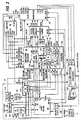
- FIGURE 2An overall block diagram for a wide screen television in accordance with inventive arrangements, and adapted to operate with 2f H horizontal scanning, is shown in FIGURE 2 and generally designated 10.
- the television 10generally comprises a video signals input section 20, a chassis or TV microprocessor 216, a wide screen processor 30, a 1f H to 2f H converter 40, a deflection circuit 50, an RGB interface 60, a YUV to RGB converter 240, kine drivers 242, direct view or projection tubes 244 and a power supply 70.
- the grouping of various circuits into different functional blocksis made for purposes of convenience in description, and is not intended as limiting the physical position of such circuits relative to one another.
- the video signals input section 20is adapted for receiving a plurality of composite video signals from different video sources.
- the video signalsmay be selectively switched for display as main and auxiliary video signals.
- An RF switch 204has two antenna inputs ANT1 and ANT 2. These represent inputs for both off-air antenna reception and cable reception.
- the RF switch 204controls which antenna input is supplied to a first tuner 206 and to a second tuner 208.
- the output of first tuner 206is an input to a one-chip 202, which performs a number of functions related to tuning, horizontal and vertical deflection and video controls.
- the particular one-chip shownis industry designated type TA7777.
- the baseband video signal VIDEO OUT developed in the one-chip and resulting from the signal from first tuner 206is an input to both video switch 200 and the TV1 input of wide screen processor 30.
- Other baseband video inputs to video switch 200are designated AUX1 and AUX 2. These might be used for video cameras, laser disc players, video tape players, video games and the like.
- the output of the video switch 200, which is controlled by the chassis or TV microprocessor 216is designated SWITCHED VIDEO.
- the SWITCHED VIDEOis another input to wide screen processor 30.
- a switch SW1 wide screen processorselects between the TV1 and SWITCHED VIDEO signals as a SEL COMP OUT video signal which is an input to a Y/C decoder 210.
- the Y/C decoder 210may be implemented as an adaptive line comb filter.
- Two further video sources S1 and S2are also inputs to the Y/C decoder 210.
- Each of S1 and S2represent different S-VHS sources, and each consists of separate luminance and chrominance signals.
- a switchwhich may be incorporated as part of the Y/C decoder, as in some adaptive line comb filters, or which may be implemented as a separate switch, is responsive to the TV microprocessor 216 for selecting one pair of luminance and chrominance signals as outputs designated Y_M and C_IN respectively.
- the selected pair of luminance and chrominance signalsis thereafter considered the main signal and is processed along a main signal path.
- Signal designations including _M or _MNrefer to the main signal path.
- the chrominance signal C_INis redirected by the wide screen processor back to the one-chip, for developing color difference signals U_M and V_M.
- Uis an equivalent designation for (R-Y)
- Vis an equivalent designation for (B-Y).
- the Y_M, U_M, and V_M signalsare converted to digital form in the wide screen processor for further signal processing.
- the second tuner 208functionally defined as part of the wide screen processor 30, develops a baseband video signal TV2.
- a switch SW2selects between the TV2 and SWITCHED VIDEO signals as an input to a Y/C decoder 220.
- the Y/C decoder 220may be implemented as an adaptive line comb filter.
- Switches SW3 and SW4select between the luminance and chrominance outputs of Y/C decoder 220 and the luminance and chrominance signals of an external video source, designated Y_EXT and C_EXT respectively.
- the Y_EXT and C_EXT signalscorrespond to the S-VHS input S1.
- the Y/C decoder 220 and switches SW3 and SW4may be combined, as in some adaptive line comb filters.
- the output of switches SW3 and SW4is thereafter considered the auxiliary signal and is processed along an auxiliary signal path.
- the selected luminance outputis designated Y_A.
- Signal designations including _A, _AX and _AUXrefer to the auxiliary signal path.
- the selected chrominanceis converted to color difference signals U_A and V_A.
- the Y_A, U_A and V_A signalsare converted to digital form for further signal processing.
- the arrangement of video signal source switching in the main and auxiliary signal pathsmaximizes flexibility in managing the source selection for the different parts of the different picture display formats.
- a composite synchronizing signal COMP SYNC, corresponding to Y_Mis provided by the wide screen processor to a sync separator 212.
- the horizontal and vertical synchronizing components H and Vrespectively are inputs to a vertical countdown circuit 214.
- the vertical countdown circuitdevelops a VERTICAL RESET signal which is directed into the wide screen processor 30.
- the wide screen processorgenerates an internal vertical reset output signal INT VERT RST OUT directed to the RGB interface 60.
- a switch in the RGB interface 60selects between the internal vertical reset output signal and the vertical synchronizing component of the external RGB source. The output of this switch is a selected vertical synchronizing component SEL_VERT_SYNC directed to the deflection circuit 50.
- Horizontal and vertical synchronizing signals of the auxiliary video signalare developed by sync separator 250 in the wide screen processor.
- the 1f H to 2f H converter 40is responsible for converting interlaced video signals to progressively scanned noninterlaced signals, for example one wherein each horizontal line is displayed twice, or an additional set of horizontal lines is generated by interpolating adjacent horizontal lines of the same field. In some instances, the use of a previous line or the use of an interpolated line will depend upon the level of movement which is detected between adjacent fields or frames.
- the converter circuit 40operates in conjunction with a video RAM 420.
- the video RAMmay be used to store one or more fields of a frame, to enable the progressive display.
- the converted video data as Y_2f H , U_2f H and V_2f H signalsis supplied to the RGB interface 60.
- the RGB interface 60shown in more detail in FIGURE 14, enables selection of the converted video data or external RGB video data for display by the video signals input section.
- the external RGB signalis deemed to be a wide format display ratio signal adapted for 2f H scanning.
- the vertical synchronizing component of the main signalis supplied to the RGB interface by the wide screen processor as INT VERT RST OUT, enabling a selected vertical sync (f Vm or f Vext ) to be available to the deflection circuit 50. Operation of the wide screen television enables user selection of an external RGB signal, by generating an internal/external control signal INT/EXT.
- the RGB interface circuitdetects an external synchronizing signal, in order to override the selection of a non-existent external RGB input.
- the WSP microprocessor 340also supplies color and tint controls for the external RGB signal.
- the wide screen processor 30comprises a picture in picture processor 320 for special signal processing of the auxiliary video signal.
- the term picture-in-pictureis sometimes abbreviated as PIP or pix-in-pix.
- a gate array 300combines the main and auxiliary video signal data in a wide variety of display formats, as shown by the examples of FIGURES 1(b) through 1(i).
- the picture-in-picture processor 320 and gate array 300are under the control of a wide screen microprocessor (WSP ⁇ P) 340.
- Microprocessor 340is responsive to the TV microprocessor 216 over a serial bus.
- the serial busincludes four signal lines, for data, clock signals, enable signals and reset signals.
- the wide screen processor 30also generates a composite vertical blanking/reset signal, as a three level sandcastle signal.
- the vertical blanking and reset signalscan be generated as separate signals.
- a composite blanking signalis supplied by the video signal input section to the RGB interface.
- the deflection circuit 50receives a vertical reset signal from the wide screen processor, a selected 2f H horizontal synchronizing signal from the RGB interface 60 and additional control signals from the wide screen processor. These additional control signals relate to horizontal phasing, vertical size adjustment and east-west pin adjustment.
- the deflection circuit 50supplies 2f H flyback pulses to the wide screen processor 30, the 1f H to 2f H converter 40 and the YUV to RGB converter 240.
- Operating voltages for the entire wide screen televisionare generated by a power supply 70 which can be energized by an AC mains supply.
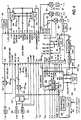
- the wide screen processor 30is shown in more detail in FIGURE 3.
- the principal components of the wide screen processorare a gate array 300, a picture-in-picture circuit 301, analog to digital and digital to analog converters, the second tuner 208, a wide screen processor microprocessor 340 and a wide screen output encoder 227. Further details of the wide screen processor, which are in common with both the 1f H and the 2f H chassis, for example the PIP circuit, are shown in FIGURE 4.
- a picture-in-picture processor 320which forms a significant part of the PIP circuit 301, is shown in more detail in FIGURE 5.
- the gate array 300is shown in more detail in FIGURE 6. A number of the components shown in FIGURE 3, forming parts of the main and auxiliary signal paths, have already been described in detail.
- the second tuner 208has associated therewith an IF stage 224 and an audio stage 226.
- the second tuner 208also operates in conjunction with the WSP ⁇ P 340.
- the WSP ⁇ P 340comprises an input output I/O section 340A and an analog output section 340B.
- the I/O section 340Aprovides tint and color control signals, the INT/EXT signal for selecting the external RGB video source and control signals for the switches SW1 through SW6.
- the I/O sectionalso monitors the EXT SYNC DET signal from the RGB interface to protect the deflection circuit and cathode ray tube(s).
- the analog output section 340Bprovides control signals for vertical size, east-west adjust and horizontal phase, through respective interface circuits 254, 256 and 258.
- the gate array 300is responsible for combining video information from the main and auxiliary signal paths to implement a composite wide screen display, for example one of those shown in the different parts of FIGURE 1.
- Clock information for the gate arrayis provided by phase locked loop 374, which operates in conjunction with low pass filter 376.
- the main video signalis supplied to the wide screen processor in analog form, and Y U V format, as signals designated Y_M, U_M and V_M. These main signals are converted from analog to digital form by analog to digital converters 342 and 346, as shown in more detail in FIGURE 4.
- the color component signalsare referred to by the generic designations U and V, which may be assigned to either R-Y or B-Y signals, or I and Q signals.
- the sampled luminance bandwidthis limited to 8 MHz because the system clock rate is 1024f H , which is approximately 16 MHz.
- a single analog to digital converter and an analog switchcan be used to sample the color component data because the U and V signals are limited to 500 KHz, or 1.5 MHz for wide I.
- the select line UV_MUX for the analog switch, or multiplexer 344is an 8 MHz signal derived by dividing the system clock by 2.
- a one clock wide start of line SOL pulsesynchronously resets this signal to zero at the beginning of each horizontal video line.
- the UV_MUX linethan toggles in state each clock cycle through the horizontal line.
- the state of the UV_MUXsince the line length is an even number of clock cycles, the state of the UV_MUX, once initialized, will consistently toggle 0, 1, 0, 1, . . . , without interruption.
- the Y and UV data streams out of the analog to digital converters 342 and 346are shifted because the analog to digital converters each have 1 clock cycle of delay.
- the clock gating information from the interpolator control 349 of main signal processing path 304must be similarly delayed. Were the clock gating information not delayed, the UV data will not be correctly paired when deleted. This is important because each UV pair represents one vector. A U element from one vector cannot be paired with a V element from another vector without causing a color shift.
- V sample from a previous pairwill be deleted along with the current U sample.
- This method of UV multiplexingis referred to as 2:1:1, as there are two luminance samples for every pair of color component (U, V) samples.
- the Nyquist frequency for both U and Vis effectively reduced to one half of the luminance Nyquist frequency. Accordingly, the Nyquist frequency of the output of the analog to digital converter for the luminance component is 8 MHz, whereas the Nyquist frequency of the output of the analog to digital converter for the color components is 4 MHz.
- the PIP circuit and/or the gate arraymay also include means for enhancing the resolution of the auxiliary data notwithstanding the data compression.
- a number of data reduction and data restoration schemeshave been developed, including for example paired pixel compression and dithering and dedithering. Moreover, different dithering sequences involving different numbers of bits and different paired pixel compressions involving different numbers of bits are contemplated.
- One of a number of particular data reduction and restoration schemescan be selected by the WSP ⁇ P 340 in order to maximize resolution of the displayed video for each particular kind of picture display format.
- the gate arrayincludes interpolators which operate in conjunction with line memories, which may be implemented as FIFO's 356 and 358.
- the interpolator and FIFO'sare utilized to resample the main signal as desired.
- An additional interpolatorcan resample the auxiliary signal.
- Clock and synchronizing circuits in the gate arraycontrol the data manipulation of both the main and auxiliary signals, including the combination thereof into a single output video signal having Y_MX, U_MX and V_MX components. These output components are converted to analog form by digital to analog converters 360, 362 and 364.
- the analog form signals, designated Y, U and Vare supplied to the 1f H to 2f H converter 40 for conversion to noninterlaced scanning.
- the Y, U and V signalsare also encoded to Y/C format by encoder 227 to define a wide format ratio output signal Y_OUT_EXT/C_OUT_EXT available at panel jacks.
- Switch SW5selects a synchronizing signal for the encoder 227 from either the gate array, C_SYNC_MN, or from the PIP circuit, C_SYNC_AUX.
- Switch SW6selects between Y_M and C_SYNC_AUX as synchronizing signal for the wide screen panel output.
- Phase comparator 228is part of a phase locked loop including low pass filter 230, voltage controlled oscillator 232, divider 234 and capacitor 236.
- the voltage controlled oscillator 232operates at 32f H, responsive to a ceramic resonator or the like 238.
- the output of the voltage controlled oscillatoris divided by 32 to provide a proper frequency second input signal to phase comparator 228.
- the output of the divider 234is a 1f H REF timing signal.
- the 32f H REF and 1f H REF timing signalsare supplied to a divide by 16 counter 400.
- a 2f H outputis supplied to a pulse width circuit 402.
- Presetting divider 400 by the 1f H REF signalassures that the divider operates synchronously with the phase locked loop of the video signals input section.
- Pulse width circuit 402assures that a 2f H -REF signal will have an adequate pulse width to assure proper operation of the phase comparator 404, for example a type CA1391, which forms part of a second phase locked loop including low pass filter 406 and 2f H voltage controlled oscillator 408.
- Voltage controlled oscillator 408generates an internal 2f H timing signal, which is used for driving the progressively scanned display.
- the other input signal to phase comparator 404is the 2f H flyback pulses or a timing signal related thereto.
- phase locked loopincluding phase comparator 404 is useful for assuring that each 2f H scanning period is symmetric within each 1f H period of the input signal. Otherwise, the display may exhibit a raster split, for example, wherein half of the video lines are shifted to the right and half of the video lines are shifted to the left.
- the deflection circuit 50is shown in more detail in FIGURE 13.
- a circuit 500is provided for adjusting the vertical size of the raster, in accordance with a desired amount of vertical overscan necessary for implementing different display formats.
- a constant current source 502provides a constant quantity of current I RAMP which charges a vertical ramp capacitor 504.
- a transistor 506is coupled in parallel with the vertical ramp capacitor, and periodically discharges the capacitor responsive to the vertical reset signal.
- current I RAMPprovides the maximum available vertical size for the raster. This might correspond to the extent of vertical overscan needed to fill the wide screen display by an expanded 4 X 3 format display ratio signal source, as shown in FIGURE 1(a).
- an adjustable current source 508diverts a variable amount of current I ADJ from I RAMP , so that vertical ramp capacitor 504 charges more slowly and to a smaller peak value.
- Variable current source 508is responsive to a vertical size adjust signal, for example in analog form, generated by a vertical size control circuit.
- Vertical size adjustment 500is independent of a manual vertical size adjustment 510, which may be implemented by a potentiometer or back panel adjustment knob. In either event, the vertical deflection coil(s) 512 receive(s) driving current of the proper magnitude.
- Horizontal deflectionis provided by phase adjusting circuit 518, East-West pin correction circuit 514, a 2f H phase locked loop 520 and horizontal output circuit 516.
- the RGB interface circuit 60is shown in more detailed in FIGURE 14.
- the signal which is to be ultimately displayedwill be selected between the output of the 1f H to 2f H converter 40 and an external RGB input.
- the external RGB inputis presumed to be a wide format display ratio, progressively scanned source.
- the external RGB signals and a composite blanking signal from the video signals input section 20are inputs to an RGB td Y U V converter 610.
- the external 2f H composite synchronizing signal for the external RGB signalis an input to external synchronizing signal separator 600.
- Selection of the vertical synchronizing signalis implemented by switch 608.
- Selection of the horizontal synchronizing signalis implemented by switch 604.
- Selection of the video signalis implemented by switch 606.
- Each of the switches 604, 606 and 608is responsive to an internal/external control signal generated by the WSP ⁇ P 340.
- Selection of internal or external video sourcesis a user selection. However, if a user inadvertently selects an external RGB source, when no such source is connected or turned on, or if the external source drops out, the vertical raster will collapse, and serious damage to the cathode ray tube(s) can result. Accordingly, an external synchronizing detector 602 checks for the presence of an external synchronizing signal. In the absence of such a signal, a switch override control signal is transmitted to each of switches 604, 606 and 608, to prevent selection of the external RGB source if the signal therefrom is not present.
- the RGB to YUV converter 610also receives tint and color control signals from the WSP ⁇ P 340.
- a wide screen television in accordance with the inventive arrangementscan be implemented with 1f H horizontal scanning instead of 2f H horizontal scanning, although such a circuit is not illustrated.
- a 1f H circuitwould not require the 1f H to 2f H converter and the RGB interface. Accordingly, there would be no provision for displaying an external wide format display ratio RGB signal at a 2f H scanning rate.
- the wide screen processor and picture-in-picture processor for a 1f H circuitwould be very similar.
- the gate arraycould be substantially identical, although not all of the inputs and outputs would be utilized.
- the various resolution enhancement schemes described hereincan be generally applied without regard to whether the television operates with 1f H or 2f H scanning.
- FIGURE 4is a block diagram showing further details of the wide screen processors 30 shown in FIGURE 3 which would be the same for both a 1f H and 2f H chassis.
- the Y_A, U_A and V_A signalsare an input to the picture in picture processor 320, which can include a resolution processing circuit 370.
- the wide screen televisionaccording to aspects of this invention can expand and compress video.
- the special effects embodied by the various composite display formats illustrated in part in FIGURE 1are generated by the picture-in-picture processor 320, which can receive resolution processed data signals Y_RP, U_RP and V_RP from resolution processing circuit 370. Resolution processing need not be utilized at all times, but during selected display formats.
- the picture-in-picture processor 320is shown in more detail in FIGURE 5.
- the principal components of the picture-in-picture processorare an analog-to-digital converter section 322, an input section 324, a fast switch (FSW) and bus section 326, a timing and control section 328 and a digital-to-analog converter section 330.
- the timing and control section 328is shown in more detail in FIGURE 11.
- the picture-in-picture processor 320may be embodied as an improved variation of a basic CPIP chip developed by Thomson Consumer Electronics, Inc.
- the basic CPIP chipis described more fully in a publication entitled The CTC 140 Picture in Picture (CPIP) Technical Training Manual, available from Thomson Consumer Electronics, Inc., Indianapolis, Indiana.
- the basic special effectis a large picture having a small picture overlaying a portion thereof as shown in FIGURE 1(c).
- the large and small picturescan result from the same video signal, from different video signals and can be interchanged or swapped. Generally speaking, the audio signal is switched to always correspond to the big picture.
- the small picturecan be moved to any position on the screen or can step through a number of predetermined positions.
- a zoom featureincreases and decreases the size of the small picture, for example to any one of a number of preset sizes.
- the large and small picturesare in fact the same size.
- a usercan zoom in on the content of the single picture, for example, in steps from a ratio of 1.0:1 to 5.0:1. While in the zoom mode a user may search or pan through the picture content enabling the screen image to move across different areas of the picture. In either event, either the small picture or the large picture or the zoomed picture can be displayed in freeze frame (still picture format). This function enables a strobe format, wherein the last nine frames of video can be repeated on the screen. The frame repetition rate can be changed from thirty frames per second to zero frames per second.
- the picture-in-picture processor used in the wide screen televisiondiffers from the present configuration of the basic CPIP chip itself as described above. If the basic CPIP chip were used with a television having a 16 X 9 screen, and without a video speed up circuit, the inset pictures would exhibit aspect ratio distortion, due to the effective 4 / 3 times horizontal expansion resulting from scanning across the wider 16 X 9 screen. Objects in the picture would be horizontally elongated. If an external speed up circuit were utilized, there would be no aspect ratio distortion, but the picture would not fill the entire screen.
- the picture-in-picture processor 320is adapted for asymmetrically compressing the video data in one of a plurality of display modes.
- this mode of operationthe pictures are compressed 4:1 in the horizontal direction and 3:1 in the vertical direction.
- This asymmetric mode of compressionproduces aspect ratio distorted pictures for storage in the video RAM. Objects in the pictures are squeezed horizontally. However, if these pictures are read out normally, as for example in the channel scan mode, for display of a 16X9 format display ratio screen, the pictures appear correct. The picture fills the screen and there is no aspect ratio distortion.
- the asymmetric compression modeaccording to this aspect of the invention makes it possible to generate the special display formats on a 16 X 9 screen without external speed up circuitry.
- FIGURE 11is a block diagram of the timing and control section 328 of the picture-in-picture processor, for example a modified version of the CPIP chip described above, which includes a decimation circuit 328C for implementing the asymmetric compression as one of a plurality of selectable display modes.
- the remaining display modescan provide auxiliary pictures of different sizes.
- Each of horizontal and vertical decimation circuitscomprises a counter which is programmed for a compression factor from a table of values under the control of the WSP ⁇ P 340.
- the range of valuescan be 1:1, 2:1, 3:1 and so on.
- the compression factorscan be symmetric or asymmetric, depending upon how the table is set up. Control of the compression ratios can also be implemented by fully programmable, general purpose decimation circuits under the control of the WSP ⁇ P 340.
- the picture-in-picture processorin conjunction with a free running oscillator 348 will take Y/C input from a decoder, for example an adaptive line comb filter, decode the signal into Y, U, V color components and generate horizontal and vertical sync pulses.
- a decoderfor example an adaptive line comb filter
- These signalsare processed in the picture-in-picture processor for the various full screen modes such as zoom, freeze and channel scan.
- the sample clock(and read/write video RAM clock) is determined by the free running oscillator.
- the sample clockwill be locked to incoming video horizontal sync, which in these special cases is the same as the display clock frequency.
- Y, U, V and C_SYNCcomposite sync outputs from the picture-in-picture processor in analog form can be re-encoded into Y/C components by encode circuit 366, which operates in conjunction with a 3.58 MHz oscillator 380.
- This Y/C_PIP_ENC signalmay be connected to a Y/C switch, not shown, which enables the re-encoded Y/C components to be substituted for the Y/C components of the main signal.
- the PIP encoded Y, U, V and sync signalswould be the basis for horizontal and vertical timing in the rest of the chassis. This mode of operation is appropriate for implementing a zoom mode for the PIP, based upon operation of the interpolator and FIFO's in the main signal path.
- the picture-in-picture processor 320comprises analog to digital converting section 322, input section 324, fast switch FSW and bus control section 326, timing and control section 328 and digital to analog converting section 330.
- the picture-in-picture processor 320digitizes the video signal into luminance (Y) and color difference signals (U, V), subsampling and storing the results in a 1 megabit video RAM 350 as explained above.
- the video RAM 350 associated with the picture-in-picture processor 320has a memory capacity of 1 megabit, which is not large enough to store a full field of video data with 8-bit samples. Increased memory capacity tends to be expensive and can require more complex management circuitry.
- the smaller number of bits per sample in the auxiliary channelrepresents a reduction in quantization resolution, or bandwidth, relative to the main signal, which is processed with 8-bit samples throughout.
- This effective reduction of bandwidthis not usually a problem when the auxiliary displayed picture is relatively small, but can be troublesome if the auxiliary displayed picture is larger, for example the same size as the main displayed picture.
- Resolution processing circuit 370can selectively implement one or more schemes for enhancing the quantization resolution or effective bandwidth of the auxiliary video data.
- a number of data reduction and data restoration schemeshave been developed, including for example, paired pixel compression and dithering and dedithering.
- a dedithering circuitwould be operatively disposed downstream of the video RAM 350, for example in the auxiliary signal path of the gate array, as explained in more detail below.
- the luminance and color difference signalsare stored in an 8:1:1 six-bit Y, U ,V fashion. In other words, each component is quantized into six-bit samples. There are eight luminance samples for every pair of color difference samples.
- the picture-in-picture processor 320is operated in a mode whereby incoming video data is sampled with a 640f H clock rate locked to the incoming auxiliary video synchronizing signal instead. In this mode, data stored in the video RAM is orthogonally sampled. When the data is read out of the picture-in-picture processor video RAM 350, it is read using the same 640f H clock locked to the incoming auxiliary video signal.
- two four bit latches 352A and 352Bare used to recombine the 8-bit data blocks from the video RAM 4-bit output port.
- the four bit latchesalso reduce the data clock rate from 1280f H to 640f H .
- the video display and deflection systemis synchronized with the main video signal.
- the main video signalmust be speeded up, as explained above, to fill the wide screen display.
- the auxiliary video signalmust be vertically synchronized with the first video signal and the video display.
- the auxiliary video signalcan be delayed by a fraction of a field period in a field memory, and then expanded in a line memory. Synchronization of the auxiliary video data with main video data is accomplished by utilizing the video RAM 350 as a field memory and a first in first out (FIFO) line memory device 354 for expanding the signal.
- the size of FIFO 354is 2048 X 8.
- the size of FIFOis related to the minimum line storage capacity thought to be reasonably necessary to avoid read/write pointer collisions.
- Read/write pointer collisionsoccur when old data is read out of the FIFO before new data has an opportunity to be written into the FIFO. Read/write pointer collisions also occur when new data overwrites the memory before the old data has an opportunity to be read out of the FIFO.
- the 8-bit DATA_PIP data blocks from video RAM 350are written into 2048 x 8 FIFO 354 with the same picture-in-picture processor 640f H clock which was used to sample the video data, that is, the 640f H clock which is locked to the auxiliary signal, rather than the main signal.
- the FIFO 354is read using the display clock of 1024f H , which is locked to horizontal synchronizing component of the main video channel.
- the use of a multiple line memory (FIFO)which has independent read and write port clocks enables data which was orthogonally sampled at a first rate to be displayed orthogonally at a second rate.
- the asynchronous nature of the read and write clocksdoes require that steps be undertaken to avoid read/write pointer collisions.
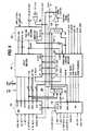
- the main signal path 304, auxiliary signal path 306 and output signal path 312 of the gate array 300are shown in block diagram form in FIGURE 6.
- the gate arrayalso comprises a clocks/sync circuit 320 and a WSP ⁇ P decoder 310. Data and address output lines of the WSP ⁇ P decoder 310, identified as WSP DATA, are supplied to each of the main circuits and paths identified above, as well as to the picture-in-picture processor 320 and resolution processing circuit 370. It will be appreciated that whether or not certain circuits are, or are not, defined as being part of the gate array is largely a matter of convenience for facilitating explanation of the inventive arrangements.
- the gate arrayis responsible for expanding, compressing and cropping video data of the main video channel, as and if necessary, to implement different picture display formats.
- the luminance component Y_MNis stored in a first in first out (FIFO) line memory 356 for a length of time depending on the nature of the interpolation of the luminance component.
- the combined chrominance components U/V_MNare stored in FIFO 358.
- Auxiliary signal luminance and chrominance components Y_PIP, U_PIP and V_PIPare developed by demultiplexer 355.
- the luminance componentundergoes resolution processing, as desired, in circuit 357, and is expanded as necessary by interpolator 359, generating signal Y_AUX as an output.
- the auxiliary displaywill be as large as the main signal display, as shown for example in FIGURE 1(d).
- the memory limitations associated with the picture-in-picture processor and video RAM 350can provide an insufficient number of data points, or pixels for filling such a large display area.
- resolution processing circuit 357can be used to restore pixels to the auxiliary video signal to replace those lost during data compression, or reduction.
- the resolution processingmay correspond to the resolution processing undertaken by circuit 370 shown in FIGURE 4.
- circuit 370may be a dithering circuit and circuit 357 may be a dedithering circuit.
- the auxiliary video input datais sampled at a 640f H rate and stored in video RAM 350.
- the auxiliary datais read out of video RAM 350 is designated VRAM_OUT.
- the PIP circuit 301also has the capability of reducing the auxiliary picture by equal integer factors horizontally and vertically, as well as asymmetrically.
- the auxiliary channel datais buffered and synchronized to the main channel digital video by the 4 bit latches 352A and 352B, the auxiliary FIFO 354, timing circuit 369 and synchronization circuit 368.
- the VRAM_OUT datais sorted into Y (luminance), U, V (color components), and FSW_DAT (fast switch data) by demultiplexer 355.
- the FSW_DATindicates which field type was written into the video RAM.
- the PIP_FSW signalis received directly from the PIP circuit and applied to the output control circuit 321 to determine which field read out of video RAM is to be displayed during the small picture modes.
- the auxiliary channelis sampled at 640f H rate while the main channel is sampled at a 1024f H rate.
- the auxiliary channel FIFO 354converts the data from the auxiliary channel sample rate to the main channel clock rate.
- the video signalundergoes an 8 / 5 ( 1024 / 640 ) compression. This is more than the 4 / 3 compression necessary to correctly display the auxiliary channel signal. Therefore, the auxiliary channel must be expanded by the interpolator 359 to correctly display a 4 X 3 small picture.
- the interpolator 359is controlled by interpolator control circuit 371, which is itself responsive to WSP ⁇ P 340.
- the amount of interpolator expansion requiredis 5 / 6 .
- the chrominance components U_PIP and V_PIPare delayed by circuit 367 for a length of time depending on the nature of the interpolation of the luminance component, generating signals U_AUX and V_AUX as outputs.
- the respective Y, U and V components of the main and auxiliary signalsare combined in respective multiplexers 315, 317 and 319 in the output signal path 312, by controlling the read enable signals of the FIFO's 354, 356 and 358.
- the multiplexers 315, 317 and 319are responsive to output multiplexer control circuit 321.
- Output multiplexer control circuit 321is responsive to the clock signal CLK, the start of line signal SOL, the H_COUNT signal, the vertical blanking reset signal and the output of the fast switch from the picture-in-picture processor and WSP ⁇ P 340.
- the multiplexed luminance and chrominance components Y_MX, U_MX and V_MXare supplied to respective digital/analog converters 360, 362 and 364 respectively.
- the digital to analog convertersare followed by low pass filters 361, 363 and 365 respectively, shown in FIGURE 4.
- the various functions of the picture-in-picture processor, the gate array and the data reduction circuitare controlled by WSP ⁇ P 340.
- the WSP ⁇ P 340is responsive to the TV ⁇ P 216, being connected thereto by a serial bus.
- the serial busmay be a four wire bus as shown, having lines for data, clock signals, enable signals and reset signals.
- the WSP ⁇ P 340communicates with the different circuits of the gate array through a WSP ⁇ P decoder 310.
- the videocan be expanded to perform horizontal zooming operations usually accompanied by vertical zooming. Horizontal zoom operations up to 33% can be accomplished by reducing compressions to less than 4/3.
- a sample interpolatoris used to recalculate the incoming video to a new pixel positions because the luminance video bandwidth, up to 5.5 MHz for S-VHS format, occupies a large percentage of the Nyquist fold over frequency, which is 8 MHz for a 1024f H clock.
- the luminance data Y_MNis routed through an interpolator 337 in the main signal path 304 which recalculates sample values based on the compression or the expansion of the video.
- the function of the switches or route selectors 323 and 331is to reverse the topology of the main signal path 304 with respect to the relative positions of the FIFO 356 and the interpolator 337. In particular, these switches select whether the interpolator 337 precedes the FIFO 356, as required for compression, or whether the FIFO 356 precedes the interpolator 337, as required for expansion.
- the switches 323 and 331are responsive to a route control circuit 335, which is itself responsive to the WSP ⁇ P 340. It will be remembered that during small picture modes the auxiliary video signal is compressed for storage in the video RAM 350, and only expansion is necessary for practical purposes. Accordingly, no comparable switching is required in the auxiliary signal path.
- the switch 323is implemented by two multiplexers 325 and 327.
- Switch 331is implemented by multiplexer 333.
- the three multiplexersare responsive to the route control circuit 335, which is itself responsive to the WSP ⁇ P 340.
- a horizontal timing/synchronization circuit 339generates timing signals controlling the writing and reading of the FIFOs, as well as latches 347 and 351, and multiplexer 353.
- the clock signal CLK and start of line signal SOLare generated by the clocks/sync circuit 320.
- An analog to digital conversion control circuit 369is responsive to Y_MN. the WSP ⁇ P 340 and the most significant bit of UV_MN.
- An interpolator control circuit 349generates intermediate pixel position values (K), interpolator compensation filter weighting (C) and clock gating information CGY for the luminance and CGUV for the color components. It is the clock gating information which pauses (decimates) or repeats the FIFO data to allow samples not to be written on some clocks for effecting compression or some samples to be read multiple times for expansion. The average slope of a ramp read out of the luminance FIFO would be 33% steeper than a corresponding input ramp. Moreover, 33% less active reading time would be required to read out the ramp as would be required to write in the data. This constitutes the 4/3 compression. It is the function of the interpolator 337 to recalculate the luminance samples.
- Expansionsmay be performed in exactly the opposite manner as compressions.
- the write enable signalhas clock gating information attached to it in the form of inhibit pulses.
- the clock gating informationis applied to the read enable signal. This will pause the data as it is being read from the FIFO 356. In this case it is the function of the interpolator, which follows the FIFO 356, to recalculate the sampled data from jagged to smooth after the expansion.
- the dataIn the expansion case the data must pause while being read from the FIFO 356 and while being clocked into the interpolator 337. This is different from the compression case where the data is continuously clocked through the interpolator 337.
- the clock gating operationscan easily be performed in a synchronous manner, that is, events can occur based on the rising edges of the 1024f H system clock.
- the clock gating operationsmay be performed in a synchronous manner. If a switchable video data topology were not used to interchange the positions of the interpolator and FIFO, the read or write clocks would need to be double clocked to pause or repeat the data.
- double clockedmeans that two data points must be written into the FIFO in a single clock cycle or read from the FIFO during a single clock cycle. The resulting circuitry cannot be made to operate synchronously with the system clock, since the writing or reading clock frequency must be twice as high as the system clock frequency.
- the switchable topologyrequires only one interpolator and one FIFO to perform both compressions and expansions. If the video switching arrangement described herein were not used, the double clocking situation can be avoided only by using two FIFO's to accomplish the functionality of both compression and expansion. One FIFO for expansions would need to be placed in front of the interpolator and one FIFO for compressions would need to be placed after the interpolator.
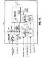
- An alternative UV signal path 530is shown in block diagram form in FIGURE 16.
- the signal path 530is very similar to the selectable topology of the luminance data in the main signal path 304 shown in FIGURES 6 and 9. The most significant difference is the use of a delay matching circuit 540 instead of interpolator 337.
- Multiplexers 534, 536 and 538enable the UV_MN signal to follow a path in which the FIFO 358 precedes the delay matching circuit 540, or a path in which the delay matching circuit 540 precedes the FIFO 358.
- the multiplexersare responsive to a route control circuit 532.
- the output of multiplexer 538is separated into the U_OUT and V_OUT signals by demultiplexer 353.
- Sorting the decimated UV pairsrequires only a 1-bit counter. This counter is synchronously reset to the U (zero) state, on the clock cycle which FIFO 358 reading starts.
- This 1-bit counteris enabled with the RD_EN_MN signal, which controls the reading of the main FIFOs 356 and 358.
- RD_EN_MNIn compression mode, RD_EN_MN is continuously high once reading starts until reading stops on each horizontal line.
- the resulting signal UV_SEL_OUTis an alternating U/V indicator which drives the select line of the demultiplexer 353. In this way, UV data samples are successfully sorted after they are read out of the FIFO 358 even though UV synchronization information could not be stored for later recall while writing the FIFO 358.
- the writing of the FIFOs 356 and 358occurs uninterrupted from the start of writing to the end of writing.
- the reading of the FIFOswill be paused, and sample values held (repeated), as they are read out of the FIFOs. This sample holding or repeating is performed by the clock gate read information which is part of the RD_EN_MN signal, and its complement, _RD_EN_MN.
- the state of the UV sampleis known as it is read from the FIFO 358.
- the UV datais written into the FIFO 358 continuously alternating U, V, U, V, ... , etc. Therefore, when the data is read out of the FIFO 358 and paused, the 1-bit counter which creates the signal UV_SEL_OUT is paused to reflect the fact that the FIFO data has been held. This keeps the sorting of demultiplexer 353 correct.
- the 1-bit counteris paused at the correct time because the RD_EN_MN signal is applied to the enable input of the 1-bit counter. This insures that as the FIFO 358 is paused, the UV_SEL_OUT signal is also paused.
- Performing expansionsdoes not require that the read enable signals for the Y and UV FIFOs 356 and 358 be separate because the clock gate read for the UV data, CGUV, is now identical to the clock gate read for the Y data, CGY.
- Performing expansionsproves easier than performing compressions.
- the color component Nyquist frequencyis not degraded during expansions and the 2:1:1 signal quality is fully maintained.
- the multiplexed color component topology described hereinhas a number of advantages.
- the methodis efficient and is ideally suited to work in conjunction with a wide bandwidth luminance raster mapping system.
- the circuit complexityis minimized while still maintaining a high degree of chrominance signal quality.
- These advantagesare due in part top the following innovations.
- the UV pairsare deleted at the input to the UV FIFO 358. This eliminates the need for carrying clock gating information through the FIFO which would require that the FIFO be another bit wider than the actual UV data precision.
- a delay matching networkis substituted for a UV interpolator, which would work in an analogous fashion to interpolator 337. This eliminates a very complicated mathematical function.
- the PIP circuit 301manipulates a 6 bit Y, U, V, 8:1:1 field memory, video RAM 350, to store incoming video data.
- the video RAM 350holds two fields of video data in a plurality of memory locations. Each memory location holds eight bits of data. In each 8-bit location there is one 6-bit Y (luminance) sample (sampled at 640f H ) and 2 other bits. These two other bits hold either fast switch data (FSW_DAT) or part of a U or V sample (sampled at 80f H ).
- the FSW_DAT valuesindicate which type of field was written into video RAM.
- the PIP circuit 301will determine which field will be read out of the memory to be displayed through the use of the fast switch data. The PIP circuit always reads the opposite field type that is being written to overcome a motion tear problem. If the field type being read is the opposite type than that being displayed, then the even field stored in the video RAM is inverted by deleting the top line of the field when the field is read out of memory. The result is that the small picture maintains correct interlace without a motion tear.
- the clocks/sync circuit 320generates read, write and enable signals needed for operating FIFOs 354, 356 and 358.
- the FIFOs for the main and auxiliary channelsare enabled for writing data into storage for those portions of each video line which is required for subsequent display. Data is written from one of the main or auxiliary channels, but not both, as necessary to combine data from each source on the same video line or lines of the display.
- the FIFO 354 of the auxiliary channelis written synchronously with the auxiliary video signal, but is read out of memory synchronously with the main video signal.
- the main video signal componentsare read into the FIFOs 356 and 358 synchronously with the main video signal, and are read out of memory synchronously with the main video. How often the read function is switched back and forth between the main and auxiliary channels is a function of the particular special effect chosen.
- FIGURES 7 and 8The process for this display format is illustrated in FIGURES 7 and 8.
- each of the FIFOsthe video data is buffered to be read out at a particular point in time.
- the active region of time where the data may be read out from each FIFOis determined by the display format chosen.
- the main channel videois being displayed on the left hand half of the display and the auxiliary channel video is displayed on the right hand half of the display.
- the arbitrary video portions of the waveformsare different for the main and auxiliary channels as illustrated.
- the read enable control signal (RD_EN_MN) of the main channel 910 x 8 FIFOsis active for 50% of the display active line period of the display beginning with the start of active video, immediately following the video back porch.
- auxiliary channel read enable control signal(RD_EN_AX) is active for the other 50% of the display active line period beginning with the falling edge of the RD_EN_MN signal and ending with the beginning of the main channel video front porch. It may be noted that write enable control signals are synchronous with their respective FIFO input data (main or auxiliary) while the read enable control signals are synchronous with the main channel video.
- the display format shown in FIGURE 1(d)is particularly desirable as it enables two nearly full field pictures to displayed in a side by side format.
- the displayis particularly effective and appropriate for a wide format display ratio display, for example 16 X 9.
- Most NTSC signalsare represented in a 4 X 3 format, which of course corresponds to 12 x 9.
- Two 4 X 3 format display ratio NTSC picturesmay be presented on the same 16 X 9 format display ratio display, either by cropping the pictures by 33% or squeezing the pictures by 33%, and introducing aspect ratio distortion.
- the ratio of picture cropping to aspect ratio distortionmay be set any where in between the limits of 0% and 33%.
- two side by side picturesmay be presented as 16.7 % squeezed and 16.7% cropped.
- the horizontal display time for a 16 X 9 format display ratio displayis the same as a 4 X3 format display ratio display, because both have 62.5 microsecond nominal line length. Accordingly, an NTSC video signal must be sped up by a factor of 4 / 3 to preserve a correct aspect ratio, without distortion.
- Variable interpolatorsare utilized in accordance with aspects of this invention to speed up the video signals. In the past, FIFOs having different clock rates at the inputs and outputs have been used to perform a similar function.
- each picturemust be distorted or cropped, or some combination thereof, by 50%. A speed up comparable to that needed for a wide screen application is unnecessary.
Landscapes
- Engineering & Computer Science (AREA)
- Multimedia (AREA)
- Signal Processing (AREA)
- Theoretical Computer Science (AREA)
- Physics & Mathematics (AREA)
- General Physics & Mathematics (AREA)
- Computer Graphics (AREA)
- Controls And Circuits For Display Device (AREA)
- Television Systems (AREA)
- Studio Circuits (AREA)
- Details Of Television Scanning (AREA)
- Transforming Electric Information Into Light Information (AREA)
- Synchronizing For Television (AREA)
- Color Television Systems (AREA)
- Stereophonic System (AREA)
- Image Processing (AREA)
- Pinball Game Machines (AREA)
- Application Of Or Painting With Fluid Materials (AREA)
- Sealing Material Composition (AREA)
- Paints Or Removers (AREA)
- Acyclic And Carbocyclic Compounds In Medicinal Compositions (AREA)
- Organic Low-Molecular-Weight Compounds And Preparation Thereof (AREA)
- Image Analysis (AREA)
- Display Devices Of Pinball Game Machines (AREA)
- Signal Processing For Digital Recording And Reproducing (AREA)
- Compositions Of Macromolecular Compounds (AREA)
- Manipulator (AREA)
- Television Signal Processing For Recording (AREA)
- Inks, Pencil-Leads, Or Crayons (AREA)
- Liquid Crystal Display Device Control (AREA)
- Control Of Indicators Other Than Cathode Ray Tubes (AREA)
- Testing, Inspecting, Measuring Of Stereoscopic Televisions And Televisions (AREA)
- Two-Way Televisions, Distribution Of Moving Picture Or The Like (AREA)
Description
Claims (1)
- A signal processing system for compressing and expanding a videosignal, comprising:characterized by:a first memory (356);means (339) for generating control signals for writing luminance data intosaid first memory (356) and for reading luminance data from said first memory(356) to delete and repeat said luminance data in order to perform luminancecompression and expansion, respectively;at least one interpolator (337) responsive to a clock control signal forresampling said luminance data;said first memory (356) and said at least one interpolator (337) introducinga first delay to the propagation of said luminance data; and,a first switching network (323, 331) for selectively establishing a firstluminance data path in which said first memory (356) precedes said at least oneinterpolator (337) for implementing said luminance data repeating and a secondluminance data path in which said at least one interpolator (337) precedes saidfirst memory (356) for implementing said luminance data deleting,a second memory (358);said means (339) adapted for generating further control signals for writingchrominance data into said second memory (358) and for reading chrominancedata from said second memory (358) to delete and repeat said chrominance datain order to perform chrominance compression and expansion, respectively, saidsecond memory (358) introducing a second delay to the propagation of saidchrominance data, said second delay being shorter than said first delay;delay means (540) responsive to said clock control signal for furtherdelaying said propagation of said chrominance data, whereby said luminance andchrominance data are realigned with one another as outputs of said signalprocessing system, and,a second switching network (534, 536, 538) for selectively establishing afirst chrominance data path in which said second memory (358) precedes saiddelay means (540) for implementing said chrominance data repeating and asecond chrominance data path in which said delay means (540) precedes saidsecond memory (358) for implementing said chrominance data deleting.
Applications Claiming Priority (3)
| Application Number | Priority Date | Filing Date | Title |
|---|---|---|---|
| GB909012326AGB9012326D0 (en) | 1990-06-01 | 1990-06-01 | Wide screen television |
| GB9012326 | 1990-06-01 | ||
| PCT/US1991/003818WO1991019398A1 (en) | 1990-06-01 | 1991-05-30 | Chrominance processing and timing system |
Publications (3)
| Publication Number | Publication Date |
|---|---|
| EP0532592A1 EP0532592A1 (en) | 1993-03-24 |
| EP0532592A4 EP0532592A4 (en) | 1994-01-05 |
| EP0532592B1true EP0532592B1 (en) | 1998-01-21 |
Family
ID=10676970
Family Applications (17)
| Application Number | Title | Priority Date | Filing Date |
|---|---|---|---|
| EP91912590ARevokedEP0532682B1 (en) | 1990-06-01 | 1991-05-29 | Synchronizing side by side pictures |
| EP91910761AExpired - LifetimeEP0533738B1 (en) | 1990-06-01 | 1991-05-29 | Asymmetric picture compression |
| EP91910567AExpired - LifetimeEP0532583B1 (en) | 1990-06-01 | 1991-05-29 | Automatic letterbox detection |
| EP97120599AExpired - LifetimeEP0831645B1 (en) | 1990-06-01 | 1991-05-29 | Automatic letterbox detection |
| EP01111808ACeasedEP1130909A3 (en) | 1990-06-01 | 1991-05-29 | Field synchronization system maintaining interlace integrity |
| EP91911604AExpired - LifetimeEP0532652B1 (en) | 1990-06-01 | 1991-05-29 | Wide screen television |
| EP19910921006WithdrawnEP0532711A4 (en) | 1990-06-01 | 1991-05-29 | Skewing dither sequences |
| EP91911605AExpired - LifetimeEP0532653B1 (en) | 1990-06-01 | 1991-05-29 | Field synchronization system with write/read pointer control |
| EP91912249AExpired - LifetimeEP0532672B1 (en) | 1990-06-01 | 1991-05-29 | Side by side television pictures |
| EP91910878AExpired - LifetimeEP0533748B1 (en) | 1990-06-01 | 1991-05-29 | Field synchronization system maintaining interlace integrity |
| EP91912116AExpired - LifetimeEP0532667B1 (en) | 1990-06-01 | 1991-05-29 | Two stage interpolation system |
| EP91910788AExpired - LifetimeEP0532592B1 (en) | 1990-06-01 | 1991-05-30 | Chrominance processing and timing system |
| EP91912548AExpired - LifetimeEP0540548B1 (en) | 1990-06-01 | 1991-05-30 | Vertical zoom and panning for television |
| EP91912342AExpired - LifetimeEP0532676B1 (en) | 1990-06-01 | 1991-05-30 | Aspect ratio control for picture overlays |
| EP91911041AExpired - LifetimeEP0532615B1 (en) | 1990-06-01 | 1991-05-30 | Picture overlay system for television |
| EP91911305AExpired - LifetimeEP0532635B1 (en) | 1990-06-01 | 1991-05-30 | Chrominance processing system |
| EP91912104AExpired - LifetimeEP0532665B1 (en) | 1990-06-01 | 1991-05-30 | Luminance processing system |
Family Applications Before (11)
| Application Number | Title | Priority Date | Filing Date |
|---|---|---|---|
| EP91912590ARevokedEP0532682B1 (en) | 1990-06-01 | 1991-05-29 | Synchronizing side by side pictures |
| EP91910761AExpired - LifetimeEP0533738B1 (en) | 1990-06-01 | 1991-05-29 | Asymmetric picture compression |
| EP91910567AExpired - LifetimeEP0532583B1 (en) | 1990-06-01 | 1991-05-29 | Automatic letterbox detection |
| EP97120599AExpired - LifetimeEP0831645B1 (en) | 1990-06-01 | 1991-05-29 | Automatic letterbox detection |
| EP01111808ACeasedEP1130909A3 (en) | 1990-06-01 | 1991-05-29 | Field synchronization system maintaining interlace integrity |
| EP91911604AExpired - LifetimeEP0532652B1 (en) | 1990-06-01 | 1991-05-29 | Wide screen television |
| EP19910921006WithdrawnEP0532711A4 (en) | 1990-06-01 | 1991-05-29 | Skewing dither sequences |
| EP91911605AExpired - LifetimeEP0532653B1 (en) | 1990-06-01 | 1991-05-29 | Field synchronization system with write/read pointer control |
| EP91912249AExpired - LifetimeEP0532672B1 (en) | 1990-06-01 | 1991-05-29 | Side by side television pictures |
| EP91910878AExpired - LifetimeEP0533748B1 (en) | 1990-06-01 | 1991-05-29 | Field synchronization system maintaining interlace integrity |
| EP91912116AExpired - LifetimeEP0532667B1 (en) | 1990-06-01 | 1991-05-29 | Two stage interpolation system |
Family Applications After (5)
| Application Number | Title | Priority Date | Filing Date |
|---|---|---|---|
| EP91912548AExpired - LifetimeEP0540548B1 (en) | 1990-06-01 | 1991-05-30 | Vertical zoom and panning for television |
| EP91912342AExpired - LifetimeEP0532676B1 (en) | 1990-06-01 | 1991-05-30 | Aspect ratio control for picture overlays |
| EP91911041AExpired - LifetimeEP0532615B1 (en) | 1990-06-01 | 1991-05-30 | Picture overlay system for television |
| EP91911305AExpired - LifetimeEP0532635B1 (en) | 1990-06-01 | 1991-05-30 | Chrominance processing system |
| EP91912104AExpired - LifetimeEP0532665B1 (en) | 1990-06-01 | 1991-05-30 | Luminance processing system |
Country Status (22)
| Country | Link |
|---|---|
| US (2) | US5285282A (en) |
| EP (17) | EP0532682B1 (en) |
| JP (20) | JP3338048B2 (en) |
| KR (16) | KR100190247B1 (en) |
| CN (15) | CN1057560A (en) |
| AU (15) | AU8084591A (en) |
| BR (1) | BR9106539A (en) |
| CA (1) | CA2082260C (en) |
| DE (19) | DE4191166T (en) |
| ES (12) | ES2124703T3 (en) |
| FI (1) | FI100931B (en) |
| GB (2) | GB9012326D0 (en) |
| HU (2) | HU225277B1 (en) |
| IN (1) | IN177990B (en) |
| MY (14) | MY108640A (en) |
| PL (1) | PL167644B1 (en) |
| PT (13) | PT97819B (en) |
| RU (1) | RU2119187C1 (en) |
| SG (11) | SG82550A1 (en) |
| TR (1) | TR25549A (en) |
| TW (3) | TW223215B (en) |
| WO (17) | WO1991019380A1 (en) |
Families Citing this family (146)
| Publication number | Priority date | Publication date | Assignee | Title |
|---|---|---|---|---|
| US5351135A (en)* | 1990-06-01 | 1994-09-27 | Thomson Consumer Electronics, Inc. | Managing letterbox signals with logos |
| US5369444A (en)* | 1990-06-01 | 1994-11-29 | Thomson Consumer Electronics | Field type matching system |
| US5345270A (en)* | 1990-06-01 | 1994-09-06 | Thomson Consumer Electronics, Inc. | Managing letterbox signals with logos and closed captions |
| US5249049A (en)* | 1990-06-01 | 1993-09-28 | Thomson Consumer Electronics, Inc. | Managing letterbox displays |
| US5309234A (en)* | 1991-05-29 | 1994-05-03 | Thomson Consumer Electronics | Adaptive letterbox detector |
| JPH04365278A (en)* | 1991-06-13 | 1992-12-17 | Matsushita Electric Ind Co Ltd | Multi-screen display circuit |
| US5414463A (en)* | 1991-09-18 | 1995-05-09 | Hitachi, Ltd. | Video cameras capable of switching an aspect ratio and view finders for use in the same |
| JPH05183833A (en)* | 1992-01-07 | 1993-07-23 | Sony Corp | Display device |
| US5287188A (en)* | 1992-01-07 | 1994-02-15 | Thomson Consumer Electronics, Inc. | Horizontal panning for wide screen television |
| EP0616466B1 (en)* | 1992-01-07 | 2000-06-07 | Thomson Consumer Electronics, Inc. | Horizontal panning for wide screen television |
| TW220024B (en)* | 1992-01-08 | 1994-02-01 | Thomson Consumer Electronics | |
| GB9200281D0 (en) | 1992-01-08 | 1992-02-26 | Thomson Consumer Electronics | A pip horizontal panning circuit for wide screen television |
| JPH05236377A (en)* | 1992-02-18 | 1993-09-10 | Sony Corp | Video selector |
| GB9205614D0 (en)* | 1992-03-14 | 1992-04-29 | Innovision Ltd | Sample rate converter suitable for converting between digital video formats |
| JP3435172B2 (en)* | 1992-06-02 | 2003-08-11 | 株式会社東芝 | Television signal processing circuit |
| EP0562221B1 (en) | 1992-03-27 | 1997-10-15 | Alcatel | Video decoder |
| JP2759727B2 (en)* | 1992-04-22 | 1998-05-28 | 日本ビクター株式会社 | Display device |
| GB2254977B (en)* | 1992-04-23 | 1996-01-17 | Philips Electronics Nv | Receiver for letterbox television signals |
| JPH0638128A (en)* | 1992-06-19 | 1994-02-10 | Sony Corp | Video image display device |
| TW234806B (en)* | 1992-07-10 | 1994-11-21 | Thomson Consumer Electronics | |
| US5262864A (en)* | 1992-07-10 | 1993-11-16 | Thomson Consumer Electronics, Inc. | Frame based vertical panning system |
| US5294987A (en)* | 1992-07-10 | 1994-03-15 | Thomson Consumer Electronics, Inc. | Field to field vertical panning system |
| JP3237783B2 (en) | 1992-08-05 | 2001-12-10 | 株式会社富士通ゼネラル | Dual screen TV receiver |
| EP0603535A1 (en)* | 1992-11-23 | 1994-06-29 | Thomson Consumer Electronics, Inc. | Tuner signal switching apparatus |
| TW335241U (en)* | 1992-11-30 | 1998-06-21 | Thomson Consumer Electronics | A video display system |
| US7168084B1 (en) | 1992-12-09 | 2007-01-23 | Sedna Patent Services, Llc | Method and apparatus for targeting virtual objects |
| US9286294B2 (en) | 1992-12-09 | 2016-03-15 | Comcast Ip Holdings I, Llc | Video and digital multimedia aggregator content suggestion engine |
| NZ259147A (en) | 1992-12-09 | 1997-05-26 | Discovery Communicat Inc | Network controller for cable television |
| US5369341A (en)* | 1992-12-11 | 1994-11-29 | Thomson Consumer Electronics, Inc. | Vertical retrace with zoom and centered fast retrace |
| US5614952A (en)* | 1994-10-11 | 1997-03-25 | Hitachi America, Ltd. | Digital video decoder for decoding digital high definition and/or digital standard definition television signals |
| TW274673B (en)* | 1993-02-10 | 1996-04-21 | Thomson Consumer Electronics | |
| JP3522273B2 (en)* | 1993-02-17 | 2004-04-26 | トムソン コンシユーマ エレクトロニクス インコーポレイテツド | Adaptive letterbox detector |
| DE69326355T2 (en)* | 1993-02-17 | 1999-12-30 | Thomson Consumer Electronics, Inc. | Arrangement and method for controlling a video display device |
| JPH06311449A (en)* | 1993-02-26 | 1994-11-04 | Sony Corp | Television receiver |
| JP3240210B2 (en) | 1993-03-10 | 2001-12-17 | トムソン コンシユーマ エレクトロニクス インコーポレイテツド | Video system |
| EP0656727B1 (en)* | 1993-11-03 | 1999-04-28 | SONY-WEGA PRODUKTIONS GmbH | Teletext receiver |
| SG80518A1 (en)* | 1993-03-15 | 2001-05-22 | Thomson Consumer Electronics | Horizontal panning for wide screen television |
| JPH06292148A (en)* | 1993-03-30 | 1994-10-18 | Sony Corp | Dual speed video display device |
| GB2308266B (en)* | 1993-03-30 | 1997-08-20 | Sony Corp | Video signal display apparatus and video signal processing circuit therefor |
| CN1050255C (en)* | 1993-04-03 | 2000-03-08 | 汤姆森消费电子有限公司 | Horizontal panning for wide screen television |
| CN1051896C (en)* | 1993-04-21 | 2000-04-26 | 汤姆森消费电子有限公司 | Managing letterbox display |
| CN1042786C (en)* | 1993-04-21 | 1999-03-31 | 汤姆森消费电子有限公司 | Video display control system |
| BE1007167A3 (en)* | 1993-05-13 | 1995-04-11 | Philips Electronics Nv | Broadcasting station for broadcasting a plurality of TELEVISION PROGRAMS, AND RECEIVER FOR RECEIVING IT. |
| US5363143A (en)* | 1993-09-03 | 1994-11-08 | Thomson Consumer Electronics, Inc. | Side by side picture display with reduced cropping |
| US5359267A (en) | 1993-09-03 | 1994-10-25 | Thomson Consumer Electronics, Inc. | Vertical deflection with vertical shrink mode |
| JP3051802B2 (en) | 1993-09-10 | 2000-06-12 | シャープ株式会社 | Video signal playback device |
| JP3022713B2 (en)* | 1993-09-30 | 2000-03-21 | 日本ビクター株式会社 | Image signal processing method |
| KR960012492B1 (en)* | 1993-11-03 | 1996-09-20 | 엘지전자 주식회사 | Vertical position varying circuit for wide tv |
| GB2284329B (en)* | 1993-11-26 | 1997-07-16 | Thomson Consumer Electronics | Emulation of computer monitor in a wide screen television |
| JP2554450B2 (en)* | 1993-12-16 | 1996-11-13 | 日本テレビ放送網株式会社 | Frame synchronizer and signal switching device using the same |
| TW312076B (en)* | 1993-12-21 | 1997-08-01 | Thomson Consumer Electronics | |
| JPH07184138A (en)* | 1993-12-24 | 1995-07-21 | Toshiba Corp | 2 screen image processing circuit |
| DE69427236T2 (en)* | 1994-01-12 | 2001-10-25 | Thomson Consumer Electronics, Inc. | VIDEO SIGNAL DECOMPRESSION SYSTEM AND MULTIMODE VIDEO UPCONVERTER |
| CN1048138C (en)* | 1994-01-12 | 2000-01-05 | 汤姆森消费电子有限公司 | Multimode interpolation filter as for a TV receiver |
| US5790197A (en)* | 1994-01-12 | 1998-08-04 | Thomson Consumer Electronics,. Inc. | Multimode interpolation filter as for a TV receiver |
| TW307971B (en)* | 1994-03-31 | 1997-06-11 | Matsushita Electric Industrial Co Ltd | |
| WO1995030303A1 (en)* | 1994-04-28 | 1995-11-09 | Kabushiki Kaisha Toshiba | Device for detecting image of letter box |
| EP0697787A3 (en)* | 1994-08-20 | 1996-05-29 | Loewe Opta Gmbh | Method and circuit for displaying a television image with 16:9 according to the PAL-plus method on the screen of a television receiver with a 16:9 image tube format |
| DE4432169A1 (en)* | 1994-09-09 | 1996-03-14 | Bosch Siemens Hausgeraete | TV |
| US5574508A (en)* | 1994-11-02 | 1996-11-12 | Rca Thomson Licensing Corporation | Vertical panning for interlaced video |
| ES2142903T3 (en)* | 1994-12-12 | 2000-05-01 | Sony Wega Produktions Gmbh | METHOD AND DEVICE TO VIEW TWO VIDEO IMAGES SIMULTANEOUSLY. |
| EP0737004A1 (en)* | 1995-04-05 | 1996-10-09 | Thomson Consumer Electronics, Inc. | Field type detector for video signal |
| GB9508289D0 (en)* | 1995-04-24 | 1995-06-14 | Rca Thomson Licensing Corp | Deflection circuits for changing display format on wide screen picture tubes |
| JP3617130B2 (en)* | 1995-07-21 | 2005-02-02 | ソニー株式会社 | Video signal processing circuit and image display device |
| DE69609264T2 (en)* | 1995-08-09 | 2001-03-15 | Koninklijke Philips Electronics N.V., Eindhoven | Device for image display with displacement of the lower image area |
| KR0176825B1 (en)* | 1995-08-16 | 1999-05-01 | 구자홍 | Image mode selection method and apparatus |
| CA2184121A1 (en)* | 1995-08-30 | 1997-03-01 | John R. Reder | Sampling analog video signal for secondary images |
| KR0144505B1 (en)* | 1995-09-18 | 1998-08-17 | 구자홍 | Automatic display device and method of image display device |
| JPH0993505A (en)* | 1995-09-26 | 1997-04-04 | Toshiba Corp | Television receiver with character multiplex decoder |
| JPH0993548A (en)* | 1995-09-27 | 1997-04-04 | Toshiba Corp | TV receiver with text information display function |
| JPH09116821A (en)* | 1995-10-18 | 1997-05-02 | Toshiba Corp | Television receiver |
| FR2742279B1 (en)* | 1995-12-06 | 1998-01-09 | Thomson Multimedia Sa | DEVICE FOR DECIMATING SEQUENCES OF DIGITAL DATA |
| US6008860A (en)* | 1995-12-29 | 1999-12-28 | Thomson Consumer Electronics, Inc. | Television system with provisions for displaying an auxiliary image of variable size |
| JP3575153B2 (en)* | 1996-01-17 | 2004-10-13 | ソニー株式会社 | Aspect ratio discrimination circuit and video monitor device |
| CA2191632A1 (en)* | 1996-02-13 | 1997-08-14 | James Lee Combs | Video processor for processing two analog composite video signals |
| CN1065396C (en)* | 1996-02-17 | 2001-05-02 | 明碁电脑股份有限公司 | Screen detection system for wide screen TV |
| DE69606852T2 (en)* | 1996-04-18 | 2000-06-29 | Matsushita Electric Industrial Co., Ltd. | Digital signal processing circuit for a television receiver |
| JPH09284671A (en)* | 1996-04-18 | 1997-10-31 | Toshiba Corp | Scan line converter |
| JPH09326958A (en)* | 1996-06-05 | 1997-12-16 | Sony Corp | Image processing unit and processing method |
| US6367080B1 (en) | 1996-08-02 | 2002-04-02 | Sanyo Electric Co., Ltd. | Internet information displaying apparatus |
| KR100206802B1 (en)* | 1996-08-20 | 1999-07-01 | 구자홍 | Automatic Wide Screen Display Method and Apparatus of TV Receiver |
| KR100678355B1 (en)* | 1996-09-27 | 2007-05-14 | 소니 가부시끼 가이샤 | Image display and control device and its method |
| US5854902A (en)* | 1996-10-31 | 1998-12-29 | Sensormatic Electronics Corporation | Video data capture and formatting in intelligent video information management system |
| JP3828992B2 (en)* | 1996-11-27 | 2006-10-04 | 三星電子株式会社 | Screen stabilization circuit for semi-wide screen television receiver |
| US6064445A (en)* | 1996-11-28 | 2000-05-16 | Samsung Electronics Co., Ltd. | Automatic picture size control method for semiwide-screen television receiver |
| DE19652362A1 (en)* | 1996-12-17 | 1998-06-18 | Thomson Brandt Gmbh | Method and device for compensating for the luminance defects resulting from the processing of chrominance signals |
| JPH1198422A (en)* | 1997-09-19 | 1999-04-09 | Sony Corp | Video signal discrimination circuit |
| JP3464924B2 (en)* | 1998-03-13 | 2003-11-10 | 株式会社東芝 | Synchronous control circuit |
| US6501507B1 (en)* | 1998-05-13 | 2002-12-31 | Barth Alan Canfield | Multimode interpolation filter as for a TV receiver |
| KR100299759B1 (en)* | 1998-06-29 | 2001-10-27 | 구자홍 | Automatic display device and method of video display device |
| GB9817421D0 (en)* | 1998-08-11 | 1998-10-07 | Danmere Limited | Interactive television control/operating system |
| CN1096181C (en)* | 1998-08-13 | 2002-12-11 | 汤姆森消费电子有限公司 | Video display control system |
| DE19911947C2 (en)* | 1999-03-17 | 2003-04-24 | Infineon Technologies Ag | Process for color edge improvement in an image overlay |
| GB2349288B (en) | 1999-04-16 | 2003-10-22 | Quantel Ltd | A video editing system |
| US6791578B1 (en) | 2000-05-30 | 2004-09-14 | Apple Computer, Inc. | 16:9 aspect ratio and anamorphic image processing |
| US7181416B2 (en)* | 2000-06-08 | 2007-02-20 | Blackstone Corporation | Multi-function transaction processing system |
| CN1199452C (en)* | 2001-06-04 | 2005-04-27 | 华为技术有限公司 | Realization method and bus interface technology of multi-group combination of multi-channel digital images |
| US7793326B2 (en) | 2001-08-03 | 2010-09-07 | Comcast Ip Holdings I, Llc | Video and digital multimedia aggregator |
| US7908628B2 (en) | 2001-08-03 | 2011-03-15 | Comcast Ip Holdings I, Llc | Video and digital multimedia aggregator content coding and formatting |
| US20030204457A1 (en)* | 2002-04-26 | 2003-10-30 | Arias Luis A. | Payee account payment system |
| DE10226071A1 (en)* | 2002-06-12 | 2004-01-08 | Fujitsu Siemens Computers Gmbh | Method and device for displaying a digitized image |
| US20060032911A1 (en)* | 2002-10-07 | 2006-02-16 | Arias Luis A | Prepaid card issuing system |
| CN100341325C (en)* | 2003-03-08 | 2007-10-03 | 中兴通讯股份有限公司 | Method of displaying fed back terminal name in digital multiple-picture meeting TV system |
| CA2523597C (en)* | 2003-04-28 | 2011-09-27 | Matsushita Electric Industrial Co., Ltd. | Recording medium, reproduction apparatus, recording method, reproducing method, program, and integrated circuit |
| DE20311377U1 (en) | 2003-07-23 | 2003-10-09 | Inova Multimedia-Systeme GmbH & Co. KG, 31137 Hildesheim | Device for displaying information in means of transport |
| KR100503091B1 (en)* | 2003-07-28 | 2005-07-21 | 삼성전자주식회사 | Method for scanning channel of digital television |
| JP3968587B2 (en)* | 2004-03-30 | 2007-08-29 | 船井電機株式会社 | Liquid crystal television, backlight control device, and backlight control method |
| CN100385926C (en)* | 2004-03-31 | 2008-04-30 | 凌阳科技股份有限公司 | liquid crystal display system with storage function |
| JP4537107B2 (en)* | 2004-04-06 | 2010-09-01 | キヤノン株式会社 | Video display device, video display method, and computer program |
| US7113200B2 (en)* | 2004-05-21 | 2006-09-26 | Polycom, Inc. | Method and system for preparing video communication image for wide screen display |
| JP4646556B2 (en)* | 2004-06-25 | 2011-03-09 | 三洋電機株式会社 | Display drive device |
| KR100640894B1 (en)* | 2004-09-07 | 2006-11-02 | 엘지전자 주식회사 | Control device and method of color liquid crystal display for mobile communication terminal |
| US7427704B2 (en)* | 2004-09-09 | 2008-09-23 | Huwaldt David A | Stringed instrument fingering guide |
| CN100584166C (en) | 2005-05-07 | 2010-01-20 | 富准精密工业(深圳)有限公司 | Liquid cooling heat radiator |
| US20070008338A1 (en)* | 2005-05-28 | 2007-01-11 | Young-Chan Kim | Display system, display apparatus, and method of controlling video source and display apparatus |
| CN100580765C (en)* | 2005-06-30 | 2010-01-13 | 康佳集团股份有限公司 | Image lattice displaying-format changing method |
| WO2007018388A1 (en)* | 2005-08-05 | 2007-02-15 | Samsung Electronics Co., Ltd. | Apparatus for providing multiple screens and method of dynamically configuring multiple screens |
| US7898600B2 (en) | 2005-08-05 | 2011-03-01 | Samsung Electronics Co., Ltd. | Apparatus for providing multiple screens and method of dynamically configuring multiple screens |
| WO2007057875A2 (en) | 2005-11-15 | 2007-05-24 | Nds Limited | Digital video zooming system |
| JP4684147B2 (en) | 2006-03-28 | 2011-05-18 | 任天堂株式会社 | Inclination calculation device, inclination calculation program, game device, and game program |
| WO2007114675A1 (en)* | 2006-04-06 | 2007-10-11 | Samsung Electronics Co., Ltd. | Apparatus for providing multiple screens and method for dynamic configuration of the same |
| FR2901947A1 (en)* | 2006-05-30 | 2007-12-07 | Nds Technologies France Soc Pa | METHOD FOR MANAGING THE DISPLAY OF A RESTRICTED VIDEO, IN PARTICULAR FOR HIGH DEFINITION TELEVISION |
| CN101946500B (en)* | 2007-12-17 | 2012-10-03 | 伊克鲁迪控股公司 | Real time video inclusion system |
| CN101483034B (en)* | 2008-02-22 | 2010-10-13 | 青岛海信电器股份有限公司 | Multiple image display method and apparatus |
| RU2380762C2 (en)* | 2008-03-05 | 2010-01-27 | Федеральное государственное унитарное предприятие "Санкт-Петербургское Опытно-конструкторское бюро "Электроавтоматика" имени П.А. Ефимова" | Visual display control device |
| JP5096247B2 (en)* | 2008-07-08 | 2012-12-12 | ルネサスエレクトロニクス株式会社 | Image processing apparatus and method |
| US9218792B2 (en) | 2008-12-11 | 2015-12-22 | Nvidia Corporation | Variable scaling of image data for aspect ratio conversion |
| US8508449B2 (en)* | 2008-12-18 | 2013-08-13 | Sharp Corporation | Adaptive image processing method and apparatus for reduced colour shift in LCDs |
| RU2488895C1 (en)* | 2009-06-17 | 2013-07-27 | Шарп Кабусики Кайся | Shift register, display control circuit, visualisation panel and visualisation device |
| EP2444958B1 (en)* | 2009-06-17 | 2017-09-20 | Sharp Kabushiki Kaisha | Shift resister, display-driving circuit, displaying panel, and displaying device |
| BR112012008070A2 (en)* | 2009-07-29 | 2016-03-01 | Sharp Kk | image display device and image display method |
| WO2011075152A1 (en) | 2009-12-18 | 2011-06-23 | Exxonmobil Research And Engineering Company | Polyalkylene epoxy polyamine additives for fouling mitigation in hydrocarbon refining processes |
| CN102107040B (en)* | 2009-12-25 | 2013-05-01 | 朝日英达科株式会社 | Guidewire |
| KR101682147B1 (en)* | 2010-04-05 | 2016-12-05 | 삼성전자주식회사 | Method and apparatus for interpolation based on transform and inverse transform |
| US8698958B2 (en)* | 2010-06-16 | 2014-04-15 | Silicon Image, Inc. | Mechanism for memory reduction in picture-in-picture video generation |
| JP5672862B2 (en) | 2010-08-27 | 2015-02-18 | ソニー株式会社 | Imaging apparatus, imaging system, and imaging method |
| RU2452125C1 (en)* | 2011-06-23 | 2012-05-27 | Федеральное государственное унитарное предприятие "Научно-производственное объединение автоматики имени академика Н.А. Семихатова" | Image processing system |
| TWI486052B (en)* | 2011-07-05 | 2015-05-21 | Realtek Semiconductor Corp | Three-dimensional image processing device and three-dimensional image processing method |
| CN103686064B (en)* | 2012-08-31 | 2017-05-03 | 杭州海康威视数字技术股份有限公司 | Picture segment display method and client-side |
| WO2014083953A1 (en)* | 2012-11-27 | 2014-06-05 | ソニー株式会社 | Display device, display method, and computer program |
| US9723216B2 (en) | 2014-02-13 | 2017-08-01 | Nvidia Corporation | Method and system for generating an image including optically zoomed and digitally zoomed regions |
| CN105389776B (en) | 2014-09-02 | 2019-05-03 | 辉达公司 | Image scaling technology |
| CN107454283B (en)* | 2016-06-01 | 2020-12-01 | 联发科技股份有限公司 | Video signal output system and method |
| CN106162262A (en)* | 2016-07-28 | 2016-11-23 | 王晓光 | Video ads receives method of reseptance and the system of side |
| US11229135B2 (en) | 2019-04-01 | 2022-01-18 | Dell Products L.P. | Multiple function chassis mid-channel |
| CN111179883B (en)* | 2020-01-03 | 2022-06-03 | 云谷(固安)科技有限公司 | Image display method and device, mobile terminal, computer equipment and storage medium |
Citations (1)
| Publication number | Priority date | Publication date | Assignee | Title |
|---|---|---|---|---|
| GB2073536A (en)* | 1980-04-09 | 1981-10-14 | British Broadcasting Corp | Television signal processing |
Family Cites Families (119)
| Publication number | Priority date | Publication date | Assignee | Title |
|---|---|---|---|---|
| BE490074A (en)* | 1948-07-09 | |||
| AT303141B (en)* | 1970-01-20 | 1972-11-10 | Siemens Ag | Arrangement for evaluating certain parts of the image |
| US3624289A (en)* | 1970-08-26 | 1971-11-30 | Data Plex Systems | Apparatus for blanking portion of fields of television video signals |
| US3878327A (en)* | 1973-10-17 | 1975-04-15 | Westinghouse Electric Corp | Television system for improving reading skills |
| US4026555A (en)* | 1975-03-12 | 1977-05-31 | Alpex Computer Corporation | Television display control apparatus |
| CH625936B (en)* | 1975-07-29 | Seiko Instr & Electronics | PORTABLE ELECTRONIC CLOCKWORK PIECE. | |
| JPS5329019A (en)* | 1976-08-30 | 1978-03-17 | Toshiba Corp | Color relevision receiver set |
| JPS6011875B2 (en)* | 1977-08-17 | 1985-03-28 | 日本電気株式会社 | Chroma key tracking device |
| US4259690A (en)* | 1977-10-06 | 1981-03-31 | Sharp Kabushiki Kaisha | Multi-picture tuning scheme of television receiver |
| US4266242A (en)* | 1978-03-21 | 1981-05-05 | Vital Industries, Inc. | Television special effects arrangement |
| DK149879A (en)* | 1978-04-12 | 1979-10-13 | Data Recall Ltd | CONTROLLER FOR USE IN VIEWING VIDEO SIGNALS |
| US4356511A (en)* | 1978-05-23 | 1982-10-26 | Sony Corporation | Digital soft-edge video special effects generator |
| US4249213A (en)* | 1978-09-14 | 1981-02-03 | Hitachi, Ltd. | Picture-in-picture television receiver |
| SE411007B (en)* | 1979-03-30 | 1979-11-19 | Globe Computers Ab | PROCEDURE AND DEVICE FOR SYNCHRONIZING A DIGITAL MEMORY WITH AN EXISTING TV SYSTEM |
| JPS5853791Y2 (en)* | 1979-05-08 | 1983-12-07 | ソニー株式会社 | image display device |
| US4282546A (en)* | 1979-11-28 | 1981-08-04 | Rca Corporation | Television image size altering apparatus |
| US4399462A (en) | 1981-01-30 | 1983-08-16 | Fairchild-Weston Systems Inc. | Video split screen technique |
| JPS57208772A (en)* | 1981-06-18 | 1982-12-21 | Sony Corp | Television receiver |
| US4460890A (en)* | 1982-01-21 | 1984-07-17 | Sony Corporation | Direct digital to digital sampling rate conversion, method and apparatus |
| DE3233288A1 (en)* | 1982-09-08 | 1984-03-08 | Robert Bosch Gmbh, 7000 Stuttgart | SYSTEM FOR TIME COMPRESSION AND / OR EXPANSION OF ELECTRICAL SIGNALS |
| US4651195A (en)* | 1983-04-04 | 1987-03-17 | Robot Research, Inc. | Monochrome-compatible color slow scan television system |
| US4524447A (en)* | 1983-05-25 | 1985-06-18 | Rca Corporation | Digital signal processing apparatus having digital dither |
| US4556900A (en)* | 1983-05-25 | 1985-12-03 | Rca Corporation | Scaling device as for quantized B-Y signal |
| US4556906A (en)* | 1983-11-15 | 1985-12-03 | Rca Corporation | Kinescope blanking scheme for wide-aspect ratio television |
| JPS60160780A (en)* | 1984-01-31 | 1985-08-22 | Nec Corp | Picture storage device for special effect |
| US4622577A (en)* | 1984-02-03 | 1986-11-11 | Rca Corporation | Decoder for extracting a 4:3 aspect ratio signal from a high definition television signal |
| JPS60180383A (en)* | 1984-02-28 | 1985-09-14 | Matsushita Electric Ind Co Ltd | television receiver |
| GB2160051A (en)* | 1984-04-26 | 1985-12-11 | Philips Electronic Associated | Video signal processing arrangement |
| GB2158318A (en)* | 1984-04-26 | 1985-11-06 | Philips Electronic Associated | Fading circuit for video signals |
| US4707742A (en)* | 1984-04-26 | 1987-11-17 | U.S. Philips Corporation | Video signal processing arrangement |
| US4573080A (en)* | 1984-06-28 | 1986-02-25 | Rca Corporation | Progressive scan television receiver with adaptive memory addressing |
| GB2164518B (en)* | 1984-09-14 | 1987-12-02 | Philips Electronic Associated | Rotating television pictures |
| JPH0712206B2 (en)* | 1984-10-01 | 1995-02-08 | 日本放送協会 | Basic device for video signal processing |
| JPH0646783B2 (en)* | 1984-10-15 | 1994-06-15 | ソニー株式会社 | Multi-scan type TV receiver |
| US4594726A (en)* | 1984-11-29 | 1986-06-10 | Rca Corporation | Dedithering circuitry in digital TV receiver |
| US4796086A (en)* | 1984-11-30 | 1989-01-03 | Fuji Photo Film Co., Ltd. | Method for converting color picture signals |
| US4694414A (en) | 1984-12-19 | 1987-09-15 | Rca Corporation | Digital delay interpolation filter with amplitude and phase compensation |
| NL8403929A (en)* | 1984-12-24 | 1986-07-16 | Philips Nv | COLOR TELEVISION TRANSMISSION -RESPECTIVE INFORMATION STORAGE SYSTEM WITH TIME MULTIPLEX ENCRYPTION AND SUITABLE INFORMATION AND RECEIVER. |
| JPS61193580A (en)* | 1985-02-21 | 1986-08-28 | Hitachi Ltd | Two-screen television receiver |
| US4651208A (en)* | 1985-03-18 | 1987-03-17 | Scientific Atlanta, Inc. | Compatibility of widescreen and non-widescreen television transmissions |
| US4652908A (en)* | 1985-03-25 | 1987-03-24 | Rca Corporation | Filtering system for processing a reduced-resolution video image |
| US4656516A (en)* | 1985-03-25 | 1987-04-07 | Rca Corporation | Vertical subsampling and memory synchronization system for a picture within a picture television receiver |
| US4654695A (en)* | 1985-03-25 | 1987-03-31 | Rca Corporation | Apparatus for reducing the resolution of video samples by truncating the most significant bits |
| US4656515A (en)* | 1985-03-25 | 1987-04-07 | Rca Corporation | Horizontal compression of pixels in a reduced-size video image utilizing cooperating subsampling and display rates |
| US4670784A (en)* | 1985-04-15 | 1987-06-02 | Cbs, Inc. | Methods for coping with non-uniform phosphor aging in dual mode television receivers |
| GB2179828B (en)* | 1985-08-14 | 1989-08-02 | Rca Corp | Selectable raster size for video display |
| US4763194A (en)* | 1985-08-14 | 1988-08-09 | Rca Licensing Corporation | Selectable raster size for video display |
| JPS6239762A (en)* | 1985-08-16 | 1987-02-20 | Nippon Mining Co Ltd | Ultrasonic flaw detection method for tubular bodies |
| US4729012A (en)* | 1985-08-30 | 1988-03-01 | Rca Corporation | Dual mode television receiver for displaying wide screen and standard aspect ratio video signals |
| US4758893A (en)* | 1985-09-23 | 1988-07-19 | Quanticon Inc. | Cinematic dithering for television systems |
| SU1418688A1 (en)* | 1985-11-29 | 1988-08-23 | Ленинградский электротехнический институт им.В.И.Ульянова (Ленина) | Information display apparatus |
| US4760455A (en)* | 1985-11-29 | 1988-07-26 | Canon Kabushiki Kaisha | Picture output device |
| AU591743B2 (en)* | 1985-12-28 | 1989-12-14 | Sony Corporation | Television receiver |
| GB8602644D0 (en)* | 1986-02-04 | 1986-03-12 | British Broadcasting Corp | Video systems |
| EP0236519B1 (en)* | 1986-03-08 | 1989-06-07 | ANT Nachrichtentechnik GmbH | Motion compensating field interpolation method using a hierarchically structured displacement estimator |
| JPH07113821B2 (en)* | 1986-04-21 | 1995-12-06 | 日本テキサス・インスツルメンツ株式会社 | Semiconductor memory device |
| JPS62263780A (en)* | 1986-05-09 | 1987-11-16 | Matsushita Electric Ind Co Ltd | High-definition television receiver |
| JPS62263781A (en)* | 1986-05-09 | 1987-11-16 | Matsushita Electric Ind Co Ltd | High definition television receiver |
| DE3787923T2 (en)* | 1986-05-12 | 1994-05-26 | Hitachi Ltd | Machine vision system. |
| FR2599201A1 (en)* | 1986-05-23 | 1987-11-27 | Trt Telecom Radio Electr | CODED PULSE DIFFERENTIAL MODULATION ENCODING DEVICE, ASSOCIATED DECODING DEVICE, AND TRANSMISSION SYSTEM COMPRISING AT LEAST ONE SUCH ENCODING OR DECODING DEVICE |
| US4768093A (en)* | 1986-06-05 | 1988-08-30 | North American Philips Corporation | Vertical pre-filter for pip television receivers |
| US4746981A (en)* | 1986-06-16 | 1988-05-24 | Imtech International, Inc. | Multiple screen digital video display |
| SU1429104A1 (en)* | 1986-08-18 | 1988-10-07 | Специальное Конструкторское Бюро "Кибернетика" С Опытным Производством Института Кибернетики Ан Азсср | Information output device |
| JPH0797838B2 (en)* | 1986-09-30 | 1995-10-18 | キヤノン株式会社 | Imaging device |
| US4743970A (en)* | 1986-10-20 | 1988-05-10 | The Grass Valley Group, Inc. | Picture transformation memory |
| US4689681A (en)* | 1986-10-24 | 1987-08-25 | The Grass Valley Group, Inc. | Television special effects system |
| JPS63146672A (en)* | 1986-12-10 | 1988-06-18 | Matsushita Electric Ind Co Ltd | television receiver |
| JPS63146671A (en)* | 1986-12-10 | 1988-06-18 | Matsushita Electric Ind Co Ltd | Television receiver |
| US4761587A (en)* | 1986-12-17 | 1988-08-02 | Rca Licensing Corporation | Multiple frequency horizontal oscillator for video apparatus |
| GB8701770D0 (en)* | 1987-01-27 | 1987-03-04 | Thorn Emi Home Electron | Video processing |
| JPH0824355B2 (en)* | 1987-01-27 | 1996-03-06 | 松下電器産業株式会社 | Television receiver |
| JP2506718B2 (en)* | 1987-02-06 | 1996-06-12 | 松下電器産業株式会社 | Television receiver |
| JPS63282790A (en)* | 1987-02-14 | 1988-11-18 | 株式会社リコー | Display controller |
| US4724487A (en)* | 1987-02-17 | 1988-02-09 | Rca Corporation | Interlace inversion detector for a picture-in-picture video signal generator |
| US4991014A (en)* | 1987-02-20 | 1991-02-05 | Nec Corporation | Key signal producing apparatus for video picture composition |
| US4839728A (en)* | 1987-03-23 | 1989-06-13 | Rca Licensing Corporation | Picture-in-picture video signal generator |
| EP0285902A3 (en)* | 1987-04-07 | 1990-10-10 | Siemens Aktiengesellschaft | Method for the data reduction of digital picture sequences |
| DE3886814T2 (en)* | 1987-05-15 | 1994-04-28 | Pioneer Electronic Corp | Process and device for image processing. |
| US4769705A (en)* | 1987-06-30 | 1988-09-06 | Rca Licensing Corporation | Deflection synchronizing apparatus |
| DE3722172A1 (en)* | 1987-07-04 | 1989-01-12 | Thomson Brandt Gmbh | METHOD AND DEVICE FOR ENLARGING A TELEVISION IMAGE |
| JPS6429178A (en)* | 1987-07-24 | 1989-01-31 | Matsushita Electric Industrial Co Ltd | Image display device |
| JP2595551B2 (en)* | 1987-08-14 | 1997-04-02 | ソニー株式会社 | Image signal processing device |
| DE3728444A1 (en)* | 1987-08-26 | 1989-03-09 | Thomson Brandt Gmbh | METHOD AND CIRCUIT FOR IMPROVING THE RESOLUTION OF DIGITAL SIGNALS |
| GB8722394D0 (en)* | 1987-09-23 | 1987-10-28 | British Telecomm | Video coder |
| US4766355A (en)* | 1987-09-25 | 1988-08-23 | Zenith Electronics Corporation | Automatic vertical size control |
| US4821086A (en)* | 1987-10-28 | 1989-04-11 | Rca Licensing Corporation | TV receiver having in-memory switching signal |
| US4831447A (en)* | 1987-11-16 | 1989-05-16 | The Grass Valley Group, Inc. | Method and apparatus for anti-aliasing an image boundary during video special effects |
| EP0318986B1 (en)* | 1987-11-30 | 1996-03-06 | Nec Corporation | Apparatus for generating a picture signal at precise horizontal position |
| JP2578852B2 (en)* | 1987-12-14 | 1997-02-05 | 松下電器産業株式会社 | High-definition television receiver |
| JPH01157181A (en)* | 1987-12-14 | 1989-06-20 | Matsushita Electric Ind Co Ltd | High definition television receiver |
| JPH01157182A (en)* | 1987-12-14 | 1989-06-20 | Matsushita Electric Ind Co Ltd | High-fidelity television receiver |
| JPH01205688A (en)* | 1988-02-10 | 1989-08-18 | Nec Corp | Television receiver |
| JPH01221067A (en)* | 1988-02-29 | 1989-09-04 | Sony Corp | Picture display device |
| JPH01248879A (en)* | 1988-03-30 | 1989-10-04 | Toshiba Corp | address control circuit |
| JP2829962B2 (en)* | 1988-04-28 | 1998-12-02 | 松下電器産業株式会社 | Television receiver |
| US4903269A (en)* | 1988-05-16 | 1990-02-20 | General Electric Company | Error detector for encoded digital signals |
| US4829378A (en)* | 1988-06-09 | 1989-05-09 | Bell Communications Research, Inc. | Sub-band coding of images with low computational complexity |
| US4910585A (en)* | 1988-06-29 | 1990-03-20 | General Electric Company | Frequency selective video signal intraframe processor |
| JPH0216881A (en)* | 1988-07-05 | 1990-01-19 | Sony Corp | Superimposing device |
| KR950010887B1 (en)* | 1988-07-08 | 1995-09-25 | Samsung Electronics Co Ltd | Multi-screen producting image control circuit |
| NL8801802A (en)* | 1988-07-15 | 1990-02-01 | Philips Nv | VIDEO SIGNAL PROCESSING CIRCUIT. |
| JPH0813126B2 (en)* | 1988-08-12 | 1996-02-07 | 沖電気工業株式会社 | Image communication device |
| US4916525A (en)* | 1988-08-29 | 1990-04-10 | Hughes Aircraft Company | High definition TV system |
| US4984078A (en)* | 1988-09-02 | 1991-01-08 | North American Philips Corporation | Single channel NTSC compatible EDTV system |
| US4941045A (en)* | 1988-10-11 | 1990-07-10 | Scientific-Atlanta, Inc. | Method and apparatus for improving vertical definition of a television signal by scan conversion |
| JPH02132980A (en)* | 1988-11-14 | 1990-05-22 | Sony Corp | Tv receiver |
| JPH02137585A (en)* | 1988-11-18 | 1990-05-25 | Sony Corp | Television receiver |
| US4984081A (en)* | 1989-01-24 | 1991-01-08 | Matsushita Electric Industrial Co., Ltd. | Apparatus for receiving and selecting high-definition television (HDTV) signals and standard television (NTSC) signals |
| GB2231460B (en)* | 1989-05-04 | 1993-06-30 | Sony Corp | Spatial interpolation of digital video signals |
| US5008752A (en)* | 1989-06-16 | 1991-04-16 | Eastman Kodak Company | Digital image interpolator with multiple interpolation algorithms |
| US4992874A (en)* | 1989-07-03 | 1991-02-12 | Rca Licensing Corporation | Method and apparatus for correcting timing errors as for a multi-picture display |
| US4987493A (en)* | 1989-08-01 | 1991-01-22 | Rca Licensing Corporation | Memory efficient interlace apparatus and method as for a picture in a picture display |
| CA2039143C (en)* | 1989-08-23 | 2000-04-25 | Enrique Rodriquez-Cavazos | Convergence control system for multiple vertical formats |
| US5027078A (en)* | 1989-10-10 | 1991-06-25 | Xerox Corporation | Unscreening of stored digital halftone images by logic filtering |
| US4965668A (en)* | 1989-11-09 | 1990-10-23 | The Grass Valley Group, Inc. | Adaptive rounder for video signals |
| US5027212A (en)* | 1989-12-06 | 1991-06-25 | Videologic Limited | Computer based video/graphics display system |
| US5021887A (en)* | 1989-12-13 | 1991-06-04 | Samsung Electronics Co., Ltd. | Method and circuit for composing still image of picture-in-picture |
| US5018090A (en)* | 1990-03-13 | 1991-05-21 | Rca Licensing Corporation | Digital interpolation circuitry |
| JP5937913B2 (en) | 2012-07-27 | 2016-06-22 | ヤンマー株式会社 | engine |
- 1990
- 1990-06-01GBGB909012326Apatent/GB9012326D0/enactivePending
- 1991
- 1991-05-24TWTW080104046Apatent/TW223215B/zhactive
- 1991-05-24TWTW080104039Apatent/TW252257B/zhactive
- 1991-05-24TWTW080104060Apatent/TW243575B/zhnot_activeIP Right Cessation
- 1991-05-25MYMYPI91000904Apatent/MY108640A/enunknown
- 1991-05-25MYMYPI91000898Apatent/MY106816A/enunknown
- 1991-05-25MYMYPI91000910Apatent/MY110220A/enunknown
- 1991-05-25MYMYPI91000906Apatent/MY106517A/enunknown
- 1991-05-25MYMYPI91000899Apatent/MY106812A/enunknown
- 1991-05-25MYMYPI91000912Apatent/MY107482A/enunknown
- 1991-05-25MYMYPI91000897Apatent/MY115270A/enunknown
- 1991-05-25MYMYPI91000913Apatent/MY110244A/enunknown
- 1991-05-25MYMYPI91000902Apatent/MY106670A/enunknown
- 1991-05-25MYMYPI91000908Apatent/MY107487A/enunknown
- 1991-05-25MYMYPI91000901Apatent/MY106666A/enunknown
- 1991-05-25MYMYPI91000903Apatent/MY106821A/enunknown
- 1991-05-25MYMYPI91000911Apatent/MY105289A/enunknown
- 1991-05-25MYMYPI91000909Apatent/MY111161A/enunknown
- 1991-05-27KRKR1019920703029Apatent/KR100190247B1/ennot_activeExpired - Lifetime
- 1991-05-29DEDE19914191166patent/DE4191166T/deactiveGranted
- 1991-05-29AUAU80845/91Apatent/AU8084591A/ennot_activeAbandoned
- 1991-05-29DEDE69132376Tpatent/DE69132376T2/ennot_activeExpired - Lifetime
- 1991-05-29HUHU9203768Apatent/HU225277B1/enunknown
- 1991-05-29JPJP51065191Apatent/JP3338048B2/ennot_activeExpired - Lifetime
- 1991-05-29EPEP91912590Apatent/EP0532682B1/ennot_activeRevoked
- 1991-05-29SGSG9608487Apatent/SG82550A1/enunknown
- 1991-05-29ESES91912249Tpatent/ES2124703T3/ennot_activeExpired - Lifetime
- 1991-05-29EPEP91910761Apatent/EP0533738B1/ennot_activeExpired - Lifetime
- 1991-05-29WOPCT/US1991/003744patent/WO1991019380A1/ennot_activeApplication Discontinuation
- 1991-05-29DEDE69127286Tpatent/DE69127286T2/ennot_activeExpired - Lifetime
- 1991-05-29SGSG1996002555Apatent/SG55018A1/enunknown
- 1991-05-29WOPCT/US1991/003739patent/WO1991019390A1/enactiveApplication Filing
- 1991-05-29DEDE69130610Tpatent/DE69130610T2/ennot_activeExpired - Lifetime
- 1991-05-29DEDE69127897Tpatent/DE69127897T2/ennot_activeRevoked
- 1991-05-29KRKR1019920703028Apatent/KR100195364B1/ennot_activeExpired - Lifetime
- 1991-05-29ESES91910878Tpatent/ES2165841T3/ennot_activeExpired - Lifetime
- 1991-05-29DEDE69127194Tpatent/DE69127194T2/ennot_activeExpired - Fee Related
- 1991-05-29DEDE69129806Tpatent/DE69129806T2/ennot_activeExpired - Lifetime
- 1991-05-29SGSG9602264Apatent/SG96156A1/enunknown
- 1991-05-29JPJP51029991Apatent/JP3333189B2/ennot_activeExpired - Fee Related
- 1991-05-29AUAU80590/91Apatent/AU8059091A/ennot_activeAbandoned
- 1991-05-29KRKR1019920703025Apatent/KR100195590B1/ennot_activeExpired - Fee Related
- 1991-05-29KRKR1019920703032Apatent/KR0183367B1/ennot_activeExpired - Fee Related
- 1991-05-29AUAU80725/91Apatent/AU8072591A/ennot_activeAbandoned
- 1991-05-29WOPCT/US1991/003745patent/WO1991019379A1/enactiveIP Right Grant
- 1991-05-29ESES97120599Tpatent/ES2151217T3/ennot_activeExpired - Lifetime
- 1991-05-29DEDE4191166Apatent/DE4191166C2/ennot_activeExpired - Fee Related
- 1991-05-29KRKR1019920703030Apatent/KR100195359B1/ennot_activeExpired - Fee Related
- 1991-05-29KRKR1019920703033Apatent/KR100195589B1/ennot_activeExpired - Lifetime
- 1991-05-29DEDE69126665Tpatent/DE69126665T2/ennot_activeExpired - Fee Related
- 1991-05-29EPEP91910567Apatent/EP0532583B1/ennot_activeExpired - Lifetime
- 1991-05-29ESES91910567Tpatent/ES2118085T3/ennot_activeExpired - Lifetime
- 1991-05-29HUHU9203768Apatent/HUT64662A/enunknown
- 1991-05-29JPJP51146591Apatent/JP3251581B2/ennot_activeExpired - Lifetime
- 1991-05-29ESES91912590Tpatent/ES2108046T3/ennot_activeExpired - Lifetime
- 1991-05-29SGSG1996002545Apatent/SG64307A1/enunknown
- 1991-05-29SGSG9602460Apatent/SG79895A1/enunknown
- 1991-05-29AUAU80643/91Apatent/AU8064391A/ennot_activeAbandoned
- 1991-05-29JPJP51173191Apatent/JP3373509B2/ennot_activeExpired - Lifetime
- 1991-05-29ESES91910761Tpatent/ES2106082T3/ennot_activeExpired - Lifetime
- 1991-05-29JPJP51121891Apatent/JP3145703B2/ennot_activeExpired - Fee Related
- 1991-05-29EPEP97120599Apatent/EP0831645B1/ennot_activeExpired - Lifetime
- 1991-05-29AUAU79073/91Apatent/AU7907391A/ennot_activeAbandoned
- 1991-05-29AUAU81858/91Apatent/AU8185891A/ennot_activeAbandoned
- 1991-05-29EPEP01111808Apatent/EP1130909A3/ennot_activeCeased
- 1991-05-29KRKR1019920703026Apatent/KR100195591B1/ennot_activeExpired - Lifetime
- 1991-05-29AUAU79095/91Apatent/AU7909591A/ennot_activeAbandoned
- 1991-05-29RURU92016547Apatent/RU2119187C1/ennot_activeIP Right Cessation
- 1991-05-29SGSG9602471Apatent/SG80522A1/enunknown
- 1991-05-29ESES91911604Tpatent/ES2128319T3/ennot_activeExpired - Lifetime
- 1991-05-29CACA002082260Apatent/CA2082260C/ennot_activeExpired - Lifetime
- 1991-05-29WOPCT/US1991/003733patent/WO1991019384A1/enactiveIP Right Grant
- 1991-05-29DEDE69130892Tpatent/DE69130892T2/ennot_activeExpired - Lifetime
- 1991-05-29WOPCT/US1991/003734patent/WO1991019393A1/enactiveIP Right Grant
- 1991-05-29WOPCT/US1991/003741patent/WO1991019385A1/enactiveIP Right Grant
- 1991-05-29PLPL91296954Apatent/PL167644B1/enunknown
- 1991-05-29JPJP51029891Apatent/JP3420234B2/ennot_activeExpired - Lifetime
- 1991-05-29EPEP91911604Apatent/EP0532652B1/ennot_activeExpired - Lifetime
- 1991-05-29EPEP19910921006patent/EP0532711A4/ennot_activeWithdrawn
- 1991-05-29AUAU79607/91Apatent/AU7960791A/ennot_activeAbandoned
- 1991-05-29ESES91911605Tpatent/ES2103814T3/ennot_activeExpired - Lifetime
- 1991-05-29JPJP51065091Apatent/JP3228420B2/ennot_activeExpired - Lifetime
- 1991-05-29JPJP91511219Apatent/JPH05507831A/enactivePending
- 1991-05-29DEDE69132822Tpatent/DE69132822T2/ennot_activeExpired - Lifetime
- 1991-05-29WOPCT/US1991/003743patent/WO1991019400A1/enactiveApplication Filing
- 1991-05-29EPEP91911605Apatent/EP0532653B1/ennot_activeExpired - Lifetime
- 1991-05-29EPEP91912249Apatent/EP0532672B1/ennot_activeExpired - Lifetime
- 1991-05-29KRKR1019920703027Apatent/KR100195361B1/ennot_activeExpired - Lifetime
- 1991-05-29JPJP91510297Apatent/JPH05508061A/enactivePending
- 1991-05-29BRBR919106539Apatent/BR9106539A/ennot_activeIP Right Cessation
- 1991-05-29WOPCT/US1991/003742patent/WO1991019395A1/enactiveIP Right Grant
- 1991-05-29AUAU80871/91Apatent/AU8087191A/ennot_activeAbandoned
- 1991-05-29WOPCT/US1991/003740patent/WO1991019388A1/enactiveIP Right Grant
- 1991-05-29EPEP91910878Apatent/EP0533748B1/ennot_activeExpired - Lifetime
- 1991-05-29JPJP51065291Apatent/JP3333191B2/ennot_activeExpired - Fee Related
- 1991-05-29EPEP91912116Apatent/EP0532667B1/ennot_activeExpired - Lifetime
- 1991-05-29WOPCT/US1991/003746patent/WO1991019397A1/ennot_activeApplication Discontinuation
- 1991-05-30WOPCT/US1991/003816patent/WO1991019387A1/enactiveIP Right Grant
- 1991-05-30DEDE69131501Tpatent/DE69131501T2/ennot_activeExpired - Lifetime
- 1991-05-30JPJP51173891Apatent/JP3298876B2/ennot_activeExpired - Fee Related
- 1991-05-30AUAU81860/91Apatent/AU8186091A/ennot_activeAbandoned
- 1991-05-30JPJP91511739Apatent/JPH05507597A/enactivePending
- 1991-05-30KRKR1019920703036Apatent/KR100195588B1/ennot_activeExpired - Fee Related
- 1991-05-30KRKR1019920703037Apatent/KR100195357B1/ennot_activeExpired - Lifetime
- 1991-05-30ESES91912342Tpatent/ES2134196T3/ennot_activeExpired - Lifetime
- 1991-05-30EPEP91910788Apatent/EP0532592B1/ennot_activeExpired - Lifetime
- 1991-05-30SGSG9602332Apatent/SG81864A1/enunknown
- 1991-05-30WOPCT/US1991/003813patent/WO1991019399A1/enactiveIP Right Grant
- 1991-05-30ININ411CA1991patent/IN177990B/enunknown
- 1991-05-30WOPCT/US1991/003810patent/WO1991019381A1/enactiveApplication Filing
- 1991-05-30EPEP91912548Apatent/EP0540548B1/ennot_activeExpired - Lifetime
- 1991-05-30DEDE69132349Tpatent/DE69132349T2/ennot_activeExpired - Fee Related
- 1991-05-30DEDE4191157Apatent/DE4191157C2/ennot_activeExpired - Fee Related
- 1991-05-30SGSG1996002431Apatent/SG75762A1/enunknown
- 1991-05-30EPEP91912342Apatent/EP0532676B1/ennot_activeExpired - Lifetime
- 1991-05-30SGSG1996003991Apatent/SG63585A1/enunknown
- 1991-05-30WOPCT/US1991/003822patent/WO1991019378A1/enactiveIP Right Grant
- 1991-05-30ESES91911041Tpatent/ES2148152T3/ennot_activeExpired - Lifetime
- 1991-05-30AUAU82115/91Apatent/AU8211591A/ennot_activeAbandoned
- 1991-05-30USUS07/945,641patent/US5285282A/ennot_activeExpired - Lifetime
- 1991-05-30DEDE69127193Tpatent/DE69127193T2/ennot_activeExpired - Fee Related
- 1991-05-30KRKR1019920703038Apatent/KR100195363B1/ennot_activeExpired - Fee Related
- 1991-05-30ESES91911305Tpatent/ES2106083T3/ennot_activeExpired - Lifetime
- 1991-05-30JPJP03510477Apatent/JP3140774B2/ennot_activeExpired - Fee Related
- 1991-05-30AUAU80839/91Apatent/AU8083991A/ennot_activeAbandoned
- 1991-05-30EPEP91911041Apatent/EP0532615B1/ennot_activeExpired - Lifetime
- 1991-05-30JPJP3510859Apatent/JP2780869B2/ennot_activeExpired - Fee Related
- 1991-05-30WOPCT/US1991/003815patent/WO1991019386A1/enactiveIP Right Grant
- 1991-05-30WOPCT/US1991/003818patent/WO1991019398A1/enactiveIP Right Grant
- 1991-05-30EPEP91911305Apatent/EP0532635B1/ennot_activeExpired - Lifetime
- 1991-05-30WOPCT/US1991/003817patent/WO1991019394A1/enactiveIP Right Grant
- 1991-05-30AUAU79967/91Apatent/AU7996791A/ennot_activeAbandoned
- 1991-05-30ESES91912548Tpatent/ES2100232T3/ennot_activeExpired - Lifetime
- 1991-05-30JPJP51047691Apatent/JP3354927B2/ennot_activeExpired - Fee Related
- 1991-05-30DEDE69128784Tpatent/DE69128784T2/ennot_activeExpired - Fee Related
- 1991-05-30USUS07/691,031patent/US5289284A/ennot_activeExpired - Lifetime
- 1991-05-30EPEP91912104Apatent/EP0532665B1/ennot_activeExpired - Lifetime
- 1991-05-30JPJP51122491Apatent/JP3247373B2/ennot_activeExpired - Fee Related
- 1991-05-30AUAU80768/91Apatent/AU8076891A/ennot_activeAbandoned
- 1991-05-30JPJP51047591Apatent/JP3310667B2/ennot_activeExpired - Fee Related
- 1991-05-30AUAU79833/91Apatent/AU7983391A/ennot_activeAbandoned
- 1991-05-30SGSG9602341Apatent/SG91239A1/enunknown
- 1991-05-30DEDE69125834Tpatent/DE69125834T2/ennot_activeExpired - Lifetime
- 1991-05-30DEDE69125936Tpatent/DE69125936T2/ennot_activeExpired - Fee Related
- 1991-05-30DEDE4191157Tpatent/DE4191157T1/enactivePending
- 1991-05-30SGSG1996002379Apatent/SG64872A1/enunknown
- 1991-05-31CNCN91103735Apatent/CN1057560A/enactivePending
- 1991-05-31PTPT97819Apatent/PT97819B/ennot_activeIP Right Cessation
- 1991-05-31PTPT97808Apatent/PT97808B/ennot_activeIP Right Cessation
- 1991-05-31CNCN91103736Apatent/CN1034545C/ennot_activeExpired - Lifetime
- 1991-05-31CNCN91103731Apatent/CN1034462C/ennot_activeExpired - Lifetime
- 1991-05-31CNCN91103734Apatent/CN1041878C/ennot_activeExpired - Fee Related
- 1991-05-31PTPT97813Apatent/PT97813B/enactiveIP Right Grant
- 1991-05-31PTPT97818Apatent/PT97818B/ennot_activeIP Right Cessation
- 1991-05-31CNCN91103508Apatent/CN1053310C/ennot_activeExpired - Lifetime
- 1991-05-31CNCN91103754Apatent/CN1036430C/ennot_activeExpired - Lifetime
- 1991-05-31CNCN91103728Apatent/CN1034466C/ennot_activeExpired - Fee Related
- 1991-05-31CNCN91103727Apatent/CN1052601C/ennot_activeExpired - Fee Related
- 1991-05-31CNCN91103730Apatent/CN1034461C/ennot_activeExpired - Lifetime
- 1991-05-31PTPT97810Apatent/PT97810B/ennot_activeIP Right Cessation
- 1991-05-31PTPT97809Apatent/PT97809B/enactiveIP Right Grant
- 1991-05-31TRTR91/0555Apatent/TR25549A/enunknown
- 1991-05-31PTPT97815Apatent/PT97815B/ennot_activeIP Right Cessation
- 1991-05-31CNCN91103742Apatent/CN1034465C/ennot_activeExpired - Fee Related
- 1991-05-31CNCN91103706Apatent/CN1034460C/ennot_activeExpired - Lifetime
- 1991-05-31CNCN91103726Apatent/CN1052600C/ennot_activeExpired - Lifetime
- 1991-05-31PTPT97816Apatent/PT97816B/ennot_activeIP Right Cessation
- 1991-05-31CNCN91103729Apatent/CN1039372C/ennot_activeExpired - Fee Related
- 1991-05-31CNCN91103732Apatent/CN1034544C/ennot_activeExpired - Lifetime
- 1991-05-31CNCN91103733Apatent/CN1041879C/ennot_activeExpired - Fee Related
- 1991-05-31PTPT97814Apatent/PT97814B/enactiveIP Right Grant
- 1991-05-31PTPT97811Apatent/PT97811B/ennot_activeIP Right Cessation
- 1991-05-31PTPT97817Apatent/PT97817B/ennot_activeIP Right Cessation
- 1991-05-31PTPT97812Apatent/PT97812B/enactiveIP Right Grant
- 1992
- 1992-11-09GBGB9223471Apatent/GB2259830B/ennot_activeExpired - Fee Related
- 1992-11-30KRKR1019920703024Apatent/KR100191409B1/ennot_activeExpired - Lifetime
- 1992-11-30KRKR1019920703034Apatent/KR100195358B1/ennot_activeExpired - Fee Related
- 1992-11-30KRKR1019920703039Apatent/KR100195360B1/ennot_activeExpired - Fee Related
- 1992-11-30KRKR1019920703040Apatent/KR100202157B1/ennot_activeExpired - Lifetime
- 1992-11-30KRKR1019920703035Apatent/KR100195362B1/ennot_activeExpired - Fee Related
- 1992-11-30FIFI925436Apatent/FI100931B/ennot_activeIP Right Cessation
- 1999
- 1999-01-12PTPT102241Apatent/PT102241B/ennot_activeIP Right Cessation
- 2001
- 2001-07-27JPJP2001228467Apatent/JP3699373B2/ennot_activeExpired - Lifetime
- 2004
- 2004-11-04JPJP2004320829Apatent/JP4227950B2/ennot_activeExpired - Lifetime
- 2006
- 2006-11-15JPJP2006309408Apatent/JP2007129728A/enactivePending
Patent Citations (1)
| Publication number | Priority date | Publication date | Assignee | Title |
|---|---|---|---|---|
| GB2073536A (en)* | 1980-04-09 | 1981-10-14 | British Broadcasting Corp | Television signal processing |
Also Published As
Similar Documents
| Publication | Publication Date | Title |
|---|---|---|
| EP0532592B1 (en) | Chrominance processing and timing system | |
| US5420643A (en) | Chrominance processing system for compressing and expanding video data | |
| US5311309A (en) | Luminance processing system for compressing and expanding video data | |
| US5434625A (en) | Formatting television pictures for side by side display | |
| US5351087A (en) | Two stage interpolation system | |
| US5467144A (en) | Horizontal panning for PIP display in wide screen television | |
| US5329369A (en) | Asymmetric picture compression | |
| US5313303A (en) | Aspect ratio control for picture overlays | |
| US5345272A (en) | Delay matching for video data during expansion and compression | |
| EP0616466B1 (en) | Horizontal panning for wide screen television | |
| US5365278A (en) | Side by side television pictures | |
| US5287188A (en) | Horizontal panning for wide screen television | |
| US5432560A (en) | Picture overlay system for television |
Legal Events
| Date | Code | Title | Description |
|---|---|---|---|
| PUAI | Public reference made under article 153(3) epc to a published international application that has entered the european phase | Free format text:ORIGINAL CODE: 0009012 | |
| 17P | Request for examination filed | Effective date:19921121 | |
| AK | Designated contracting states | Kind code of ref document:A1 Designated state(s):DE GB IT | |
| A4 | Supplementary search report drawn up and despatched | Effective date:19931116 | |
| AK | Designated contracting states | Kind code of ref document:A4 Designated state(s):DE GB IT | |
| 17Q | First examination report despatched | Effective date:19951110 | |
| GRAG | Despatch of communication of intention to grant | Free format text:ORIGINAL CODE: EPIDOS AGRA | |
| GRAG | Despatch of communication of intention to grant | Free format text:ORIGINAL CODE: EPIDOS AGRA | |
| GRAH | Despatch of communication of intention to grant a patent | Free format text:ORIGINAL CODE: EPIDOS IGRA | |
| GRAH | Despatch of communication of intention to grant a patent | Free format text:ORIGINAL CODE: EPIDOS IGRA | |
| GRAA | (expected) grant | Free format text:ORIGINAL CODE: 0009210 | |
| AK | Designated contracting states | Kind code of ref document:B1 Designated state(s):DE GB IT | |
| REF | Corresponds to: | Ref document number:69128784 Country of ref document:DE Date of ref document:19980226 | |
| ITF | It: translation for a ep patent filed | ||
| PLBE | No opposition filed within time limit | Free format text:ORIGINAL CODE: 0009261 | |
| STAA | Information on the status of an ep patent application or granted ep patent | Free format text:STATUS: NO OPPOSITION FILED WITHIN TIME LIMIT | |
| 26N | No opposition filed | ||
| REG | Reference to a national code | Ref country code:GB Ref legal event code:IF02 | |
| REG | Reference to a national code | Ref country code:GB Ref legal event code:746 Effective date:20030103 | |
| PGFP | Annual fee paid to national office [announced via postgrant information from national office to epo] | Ref country code:GB Payment date:20060403 Year of fee payment:16 | |
| PGFP | Annual fee paid to national office [announced via postgrant information from national office to epo] | Ref country code:IT Payment date:20060531 Year of fee payment:16 | |
| PGFP | Annual fee paid to national office [announced via postgrant information from national office to epo] | Ref country code:DE Payment date:20070525 Year of fee payment:17 | |
| GBPC | Gb: european patent ceased through non-payment of renewal fee | Effective date:20070530 | |
| PG25 | Lapsed in a contracting state [announced via postgrant information from national office to epo] | Ref country code:GB Free format text:LAPSE BECAUSE OF NON-PAYMENT OF DUE FEES Effective date:20070530 | |
| PG25 | Lapsed in a contracting state [announced via postgrant information from national office to epo] | Ref country code:DE Free format text:LAPSE BECAUSE OF NON-PAYMENT OF DUE FEES Effective date:20081202 | |
| PG25 | Lapsed in a contracting state [announced via postgrant information from national office to epo] | Ref country code:IT Free format text:LAPSE BECAUSE OF NON-PAYMENT OF DUE FEES Effective date:20070530 |