EP0528585B1 - Data processing system with internal instruction cache - Google Patents
Data processing system with internal instruction cacheDownload PDFInfo
- Publication number
- EP0528585B1 EP0528585B1EP92307155AEP92307155AEP0528585B1EP 0528585 B1EP0528585 B1EP 0528585B1EP 92307155 AEP92307155 AEP 92307155AEP 92307155 AEP92307155 AEP 92307155AEP 0528585 B1EP0528585 B1EP 0528585B1
- Authority
- EP
- European Patent Office
- Prior art keywords
- processor
- internal
- processors
- status
- external
- Prior art date
- Legal status (The legal status is an assumption and is not a legal conclusion. Google has not performed a legal analysis and makes no representation as to the accuracy of the status listed.)
- Expired - Lifetime
Links
Images


Classifications
- G—PHYSICS
- G06—COMPUTING OR CALCULATING; COUNTING
- G06F—ELECTRIC DIGITAL DATA PROCESSING
- G06F12/00—Accessing, addressing or allocating within memory systems or architectures
- G06F12/02—Addressing or allocation; Relocation
- G06F12/08—Addressing or allocation; Relocation in hierarchically structured memory systems, e.g. virtual memory systems
- G06F12/0802—Addressing of a memory level in which the access to the desired data or data block requires associative addressing means, e.g. caches
- G06F12/0875—Addressing of a memory level in which the access to the desired data or data block requires associative addressing means, e.g. caches with dedicated cache, e.g. instruction or stack
- G—PHYSICS
- G06—COMPUTING OR CALCULATING; COUNTING
- G06F—ELECTRIC DIGITAL DATA PROCESSING
- G06F11/00—Error detection; Error correction; Monitoring
- G06F11/36—Prevention of errors by analysis, debugging or testing of software
- G06F11/362—Debugging of software
- G06F11/3648—Debugging of software using additional hardware
- G06F11/3656—Debugging of software using additional hardware using a specific debug interface
- G—PHYSICS
- G06—COMPUTING OR CALCULATING; COUNTING
- G06F—ELECTRIC DIGITAL DATA PROCESSING
- G06F9/00—Arrangements for program control, e.g. control units
- G06F9/06—Arrangements for program control, e.g. control units using stored programs, i.e. using an internal store of processing equipment to receive or retain programs
- G06F9/30—Arrangements for executing machine instructions, e.g. instruction decode
- G06F9/38—Concurrent instruction execution, e.g. pipeline or look ahead
- G06F9/3877—Concurrent instruction execution, e.g. pipeline or look ahead using a slave processor, e.g. coprocessor
- G—PHYSICS
- G06—COMPUTING OR CALCULATING; COUNTING
- G06F—ELECTRIC DIGITAL DATA PROCESSING
- G06F11/00—Error detection; Error correction; Monitoring
- G06F11/22—Detection or location of defective computer hardware by testing during standby operation or during idle time, e.g. start-up testing
- G06F11/26—Functional testing
- G06F11/261—Functional testing by simulating additional hardware, e.g. fault simulation
Definitions
- the present inventionis generally directed to a processing system such as an arrangement for verifying, with an in circuit emulator, the instructions to be executed by a processor of a processing system.
- the present inventionis more particularly directed to such an arrangement wherein the processor includes an internal instruction cache for storing internal instructions and wherein internal execution parameters, resulting from the execution of internal instructions by the processor, are made available to the in circuit emulator.
- Processing systemsare well known in the art. Such systems generally include a processor and an external memory.
- a program counter of the processorprovides a series of memory addresses which are used by the processor for fetching instructions stored in the external memory to obtain the instructions. For each memory address, the processor conveys the memory address to the external memory over an external address bus and the external memory responds by conveying to the processor over an external instruction/data bus the instruction stored in the corresponding addressed memory location.
- processorOne well known form of processor is known in the art as a reduced instruction set computer (RISC) processor.
- RISCreduced instruction set computer
- this type of processorperforms four operations in sequence for each instruction.
- the first operationis a fetch operation to obtain the instruction from the external memory.
- the second operationis a decode operation wherein the processor decodes the instruction.
- the third operationis an execute operation wherein the processor executes the instruction and the fourth operation is a write-back operation where the processor writes a resultant from the execution back to the external memory.
- Such a processoralso generally employs a pipelined architecture to permit parallel processing. Such processing permits the processor to operate on more than one instruction at a time. For example, while the processor is fetching an instruction, it may also decode a previously fetched instruction, execute a still previously fetched instruction, and write-back a resultant from executing a still further previously fetched instruction.
- the processorgenerally operates off of a clock and performs each operation during a single clock cycle unless the pipeline is held by, for example, a trap or an exception condition.
- the processorexecutes four operations; fetch, decode, execute, and write-back.
- the instructions stored in the external memoryconstitute the program for the processor.
- circuit emulatorsare well known in the art and are used to track the execution of a processor. To do so, the in circuit emulator includes a duplicate of the program instructions in its own memory and receives from the processor, the external memory fetch addresses, the obtained instructions and data, and execution status signals. Hence, the in circuit emulators receive the external activity or state of the processor.
- GB-A-2 200 482discloses a microprocessor featuring an on-chip instruction cache and providing an additional interface signal ISF whenever a taken branch or jump is executed, allowing to monitor control flow. Additional information is also provided on the interface signals used for memory references: exception code and service address in case of an exception, virtual address of the jump in case of a taken jump.
- a single chip microprocessoris operable in a debug mode wherein it carries out external instructions in either of a master and a slave mode.
- the address signals produced by the internal program counterare sent to an external program memory during a first operation cycle; during other cycles, the corresponding port groups can be used for another object: and address latch may also be provided on the external bus.
- the inventionprovides a system for providing, externally to a first processor, an internal execution parameter resulting from the execution by the first processor of internal instructions stored in an internal instruction cache of the first processor.
- the systemincludes a second processor including an internal instruction cache for also storing the internal instructions.
- the second processoris coupled to the first processor in a master/slave configuration to enable the second processor to duplicate the instruction executions of the first processor and includes an output for providing the internal execution parameter resulting from said duplicate executions.
- the systemfurther includes external bus means coupled to the second processor output and being external to the first and second processors for making available the execution parameter externally to the first and second processors.
- the second processormay also include a second status output coupled to the in circuit emulator for providing the in circuit emulator with status signals indicative of the execution status of the instruction executions of the processors.
- the first and second processorsmay be configurable for executing instructions at an operating rate which is multiple of the operating rate of the external memory and the second processor is configurable for providing, at the second status output, the status signals indicative of the execution status of the processors for each operating cycle of the processors.
- the system 10generally includes a first processor 12, a second processor 14, an external instruction/data memory 16, and an in circuit emulator 18.
- the system 10is configured to permit the in circuit emulator 18 to verify the execution by the processors 12 and 14 of the execution instructions to be executed by the processors.
- the first processor 12 and second processor 14are coupled together in a master/slave configuration to permit the second processor 14, which is the slave processor, to duplicate the instructions performed by the first processor 12, which is the master processor.
- the external memory 16is of the type which stores instructions to be executed by the processors, data required by the processors in their executions, and resultants which are written back to the external memory 16.
- the instructions, data, and resultantsare stored in addressable storage locations of the external memory 16 and are addressable by the first processor 12 to permit processor 12 to fetch the instructions and data and to store resultants.
- the external memory 16includes a multiple-bit REQUESTS input 17 which is coupled to a multiple-bit REQUESTS output 20 of the first processor 12 by an external control bus 22.
- the requests generated by the first processor 12indicate to the external memory 16 whether an access to the external memory is a load access for fetching instruction or data or a store access for storing a resultant.
- the external memory 16further includes a 32-bit address input 24 which is coupled to a 32-bit address output 26 of the first processor 12 by an external address bus 28.
- the first processor 12For each access to the external memory 16 the first processor 12 generates an address at the address output 26 which is conveyed to the external memory by the external address bus 28 for fetching the instructions or data stored in the external memory 16 at the corresponding address or for storing a resultant at the corresponding memory address of the external memory 16.
- the first processor 12For receiving an instruction or data from the external memory 16 or for providing a resultant to the external memory 16, the first processor 12 includes a multiple-bit instruction/data port 30 which is coupled to a multiple-bit external memory instruction/data port 32 of the memory 16 by an external instruction/data bus 34.
- the second processor 14includes a multiple-bit instruction/data input 36 which is coupled to the external instruction/data bus 34.
- the input 36is an input only and the system 10 is configured so that only the first processor 12 addresses the external memory 16 for fetching instructions and data for both processors.
- the first processor 12includes a clock input 40 and the second processor 14 includes a clock input 42.
- the clock inputs 40 and 42are coupled together by an INCLOCK line 44 which is adapted to be coupled to an external clock source (not shown).
- the first processor 12is preferably arranged to derive from the clock pulses received at input 40 a memory clock which is provided at an output 46.
- processor 12is of the type which is arranged for generating memory clock pulses at a rate which is equal to the processing rate of the processors 12 and 14 corresponding to a 1X mode of operation or at a rate which is one half the processing rate of the processors 12 and 14 corresponding to a .5X mode of operation.
- the first processor 12 and second processor 14further include a 5-bit JTAG (Joint Test Action Group) input 54 and 56 respectively which, as well known in the art, may be utilized for setting the first and second processors 12 and 14 respectively into the master/slave configuration as contemplated by the present invention.
- JTAG inputsare becoming standard in logic devices and microprocessors to allow an asynchronous boundary scan chain to connect all the inputs and outputs of such devices together and make them addressable. It also allows special test instructions or modes to be defined and implemented while using the standard protocol to enable them. Hence, it is a convenient way to change the mode of a processor, as for example, to move the processor to the slave tracking state without requiring special external logic or pins.
- the JTAG inputs 54 and 56may also be utilized for placing the microprocessors 12 and 14 into other modes of operation as well.
- the microprocessors 12 and 14are configured for executing instructions stored externally in the external memory 16.
- the in circuit emulator 18includes a multiple-bit address input 60 which is coupled to the external address bus 28 and an instruction/data input 62 which is coupled to the external instruction/data bus 34.
- the first processor 12includes a 3-bit status output 52 which is coupled to a first 3-bit status input 64 of the in circuit emulator 18.
- the 3-bit status signals provided at the status output 52as well known in the art can provide a great degree of information as to the state of execution of the processor 12.
- the three status bitsmay provide, for example, information as to the state of execution as indicated in the table below.
- the system 10is capable of providing the in circuit emulator 18 with sufficient information to track the executions of the processors 12 and 14 of external instructions stored in the external memory 16.
- each of the processors 12 and 14includes an internal instruction cache 13 and 15 respectively.
- Such internal instruction cachesare provided within processors because an access to an internal cache generally requires less time than accesses to external memory.
- a processoraccesses an internal cache, there is no detectable external activity generated by a processor.
- the only way that an in circuit emulator could track internal executions of internally stored instructionswas to totally duplicate the internal instructions stored within an internal cache within the in circuit emulator.
- the second processor 14is able to provide the in circuit emulator 18 with internal execution parameters resulting from the processors executing internal instructions stored within the internal instruction caches 13 and 15.
- an internal execution parametermay be program counter value, absolute register file number on a read or a virtual address of a load/store.
- such an execution parametercould be a data element driven into the register file on a write, or an absolute register file number on a write.
- the internal execution parameter to be provided by the processor 14is the address of the internal caches 13 and 15 for a non-sequential fetch to the internal caches. This, when combined with the information of when the pipeline is advanced, stalled, branching, or taking a trap, can give the in circuit emulator the instruction trace information it needs.
- the second or slave processor 14provides the non-sequential fetch address at its multiple-bit address output 70.
- the address output 70is coupled to a second address input 72 of the in circuit emulator by another external address bus 71.
- the second processor 14will provide at its output 70 the exact address of the internal cache storage location being addressed.
- Such non-sequential addressesare known in the art as jump addresses.
- the second processor 14will continue to provide the current non-sequential fetch address until the next non-sequential fetch occurs.
- both processors 12 and 14execute the program from external memory 16 at the same time, but only the master processor 12 is allowed to drive the external bus. This is accomplished by tieing all the inputs and outputs of the two processors together and by setting processor 14 into the slave mode through the JTAG input 56 to prevent it from ever driving an output value. As a result, both processors run the same program, but only processor 12 drives the value for stores to the external memory 16. Because of this relationship, the address bus 71 of the slave processor 14 is not needed for instruction fetches, loads, and stores, since the master processor 12 drives the value.
- the second processor 14also includes a 3-bit status output 74 which is coupled to a second status input 76 of the in circuit emulator.
- the status signals provided at the status output 74will be identical to the status signals provided at the status output 52 of the first processor 12.
- the status signals provided at output 74can be modified by encoding in a manner as will be appreciated by those skilled in the art to provide, for example, the information illustrated in the table below.
- the first processor 12will continue to provide at its status output 52 the execution status for each operating cycle of the external memory 16.
- the second processor 14will provide at its status output 74 status signals indicative of the execution status of the processor for each operating cycle of the processors.
- the processorswill execute two operating cycles for each operating cycle of the external memory.
- the status output 74 of the second processor 14when the processors are operating in the .5X mode, will reflect the exact execution status of the processors 12 and 14.
- the in circuit emulator 18is provided with an exact cycle by cycle breakdown of the instruction stream of the processors 12 and 14 without physically duplicating the entire instruction caches externally. This therefore provides a high degree of accuracy and visibility of the microprocessor executions for verifying the instructions to be executed by the processors.
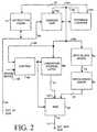
- FIG 2it illustrates in greater detail the manner in which the second processor 14 provides the non-sequential jump addresses to its external address bus 71 when the processors 12 and 14 issue a non-sequential address for accessing the internal caches 13 and 15.
- the internal cache of the second processor 14is referenced in Figure 2 by the reference character 15.
- Common to both processorsare a program counter 80, an address unit 82, a next block adder 84, a fetch-ahead adder 86, a latch 88, a multiplexer 90, an internal instruction bus 92 and a second internal address bus 94.
- the program counter 80generates an initial address which is utilized by the next-block adder 84 and the fetch-ahead adder 86 to generate sequential addresses within address blocks of the external memory 16.
- the address unit 82sets the program counter 80 to the non-sequential fetch address which is conveyed to the instruction cache 15 over the second internal address bus 94.
- the second processor 14includes a control means 96.
- the program counter 80is coupled to the control means 96 and the latch 88 by a first internal address bus 98.
- the control means 96includes a control input 100 which is set when the JTAG input 56 is set to condition the second processor 14 for master/slave operation.
- a non-sequential fetch addressis provided by the program counter 80, the non-sequential address is conveyed to the latch 88 and the control means 96 by the first internal address bus 98.
- the control means 96causes the non sequential address to be latched in the latch 88.
- the control means 96also is coupled to the multiplexer 90 and causes the multiplexer to select input 102 for conveying the non-sequential address from the latch 88 through the multiplexer 90 and onto the external address bus 71 couple to the second processor 14.
- the non-sequential addressis held on the bus 71 until the next non-sequential address is provided by the program counter 80 and detected by the control means 96.
- the second processor 14is arranged to provide the internal jump address to the in circuit emulator 18 over the external address bus 71.
- additional slave processorsmay be added to the system 10 of Figure 1 for providing other internal execution parameters with only slight modification to the existing hardware.
- Figure 3illustrates a series of wave forms which may be referenced to lend further understanding of the present invention.
- Figure 3illustrates four memory clock operating cycles including a first cycle from T0 to T1, a second cycle from T1 to T2, a third cycle from T2 to T3, and fourth cycle from T3 to T4.
- the first processor 12provides at its status output 52 an indication that it is currently executing on an instruction.
- the first processor 12provides a load request from its request output 20 and a load address at its address output 26. This is an external access to the external memory 16.
- the first processor 12indicates at its status output 52, that it is currently executing.
- the program counters of the processors 12 and 14issue a non-sequential fetch address to the internal caches 13 and 15.
- such an internal accessis not evident by the external activity of the first processor 12.
- the second or slave processor 14issues at its address output 70 the non-sequential fetch address to the internal caches which is the exact address of the caches being accessed.
- the in circuit emulator 18is provided with the non-sequential fetch address and is able to track the internal executions of the processors 12 and 14.
- the external memory 16provides the requested data responsive to the access initiated by the first processor 12 at time T1.
- the dataappears on the external instruction/data bus 34 and is received by both the first processor 12 and the second processor 14.
- the processor 12indicates at its status output 52 that it has provided a non-sequential fetch address which, as previously mentioned, is provided by the second processor 14 at its address output 70.
- the first processorindicates at its status output 52 that it is currently executing. Also during the fourth cycle, it will be noted that the second or slave processor 14 continues to hold the non-sequential fetch address at its address output 70.
- the wave forms referred to aboverelate to the operation of the processors 12 and 14 when in the 1X mode.
- the status output of the second processor from its status output 74is not shown in Figure 3 for this mode of operation since it would indicate the same execution status as that provided by the first processor 12.
- the bottom wave formillustrates the status indications which may be provided by the second or slave processor 14 when the processors 12 and 14 are operating in the .5X mode.
- the second processor 14indicates the execution status of both processors for each operating cycle of the processors. Since the processors when operating in the .5X mode are operating at a rate which is twice the operating rate of the external memory, the second processor 14 during each memory clock cycle will indicate the execution status of the processors for two processor operating cycles.
- the second processor 14indicates that the processors were in a branch state during the first microprocessor cycle and then in an execution state during the second microprocessor cycle of the third memory clock cycle between times T2 and T3.
- the second or slave processor 14is not only able to provide an internal execution parameter externally to the processors 12 and 14, it additionally is enabled to provide an exact indication of the execution status of the processors for each operating cycle while the first processor 12 provides a status indication of the execution of the processors for each memory clock cycle.
- each of the processors 12 and 14is preferably an Am29030/35 microprocessor manufactured by Advanced Micro Devices.
- the present inventionmay be employed to advantage in association with virtually any like plurality of microprocessors.
- the present embodimentovercomes the difficulty in providing an in circuit emulator with all instructions that are internally being executed by a processor.
- all such instructionsare provided to the in circuit emulator on a real time basis for duplicating the actual timing of the processor.
- additional slave processorsmay be added with each separately configured to provide a different key internal state to an external in circuit emulator for break-pointing purposes. This is made possible since the external address bus of a slave processor is always idle.
- the present embodimentis capable of providing an external in circuit emulator with many different internal execution parameters with the addition of a separate slave processor for each such internal execution parameter to be provided.
- the foregoingrepresents a powerful tool in verifying instructions to be executed by a processor since large on-chip caches are becoming increasingly popular for use in microprocessors.
- the slave processor 14watches and duplicates the request and instructions obtained by the master processor 12 and thus duplicates the executions of the master.
- the external address bus 71will latch the address value of the jump and drive it externally on the next memory clock cycle rising edge.
- the slave processor 14will provide the external in circuit emulator with the exact address of every jump and not the pre-fetch address. It will continue to drive this value until the next non-sequential fetch is performed by the processors.
Landscapes
- Engineering & Computer Science (AREA)
- Theoretical Computer Science (AREA)
- Physics & Mathematics (AREA)
- General Engineering & Computer Science (AREA)
- General Physics & Mathematics (AREA)
- Computer Hardware Design (AREA)
- Software Systems (AREA)
- Quality & Reliability (AREA)
- Test And Diagnosis Of Digital Computers (AREA)
- Debugging And Monitoring (AREA)
Abstract
Description
| STAT | CYCLE |
| 000 | Halt or Step |
| 001 | Pipeline Hold |
| 010 | Load Test Instruction |
| 011 | |
| 100 | Interrupt Return |
| 101 | Taking Interrupt or Trap |
| 110 | Non-sequential Fetch |
| 111 | Executing Mode |
| STAT | Cycle i | Cycle i + 1 |
| 000 | pipehold | pipehold |
| 001 | pipehold | executing |
| 010 | executing | pipehold |
| 011 | executing | executing |
| 100 | pipehold | branch |
| 101 | branch | pipehold |
| 110 | executing | branch |
| 111 | branch | executing |
Claims (13)
- A system for providing, externally to a first processor (12), aninternal execution parameter resulting from the execution by said firstprocessor of internal instructions stored in an internal instruction cache(13) of said first processor, being characterised by said system further comprising:a second processor (14) including an internal instruction cache (15)for also storing said internal instructions, said second processor beingcoupled to said first processor in a master/slave configuration to enablesaid second processor to duplicate the instruction executions of said firstprocessor, said second processor including an output (70) for providingthe internal execution parameter resulting from said duplicate executions; andbus means (71) coupled to said second processor output and beingexternal to said first and second processors for making available said internal executionparameter externally to said first and second processors.
- A system as claimed in claim 1 wherein said second processorincludes latch means (88) for latching said internal execution parameterat said output.
- A system as claimed in claim 2 wherein said second processorfurther includes control means (96) for detecting the occurrence of saidinternal execution parameter, said control means being coupled to saidlatch means for causing said latch means to latch said internal executionparameter.
- A system as claimed in claim 3 wherein said second processorincludes an internal bus means (98) for carrying said internal executionparameter and wherein said latch means and said control means arecoupled to said internal bus means.
- A system as claimed in claim 4 wherein said internal executionparameter is a non-sequential fetch address to said first and secondprocessor internal instruction caches.
- A system as claimed in claim 5 wherein said second processorfurther includes a program counter (80) for providing said non-sequentialfetch address and wherein said program counter is coupled to said secondprocessor internal instruction cache by said internal bus means.
- A system as claimed in claim 6 wherein said internal bus meanscomprises a first internal address bus (98) for coupling said programcounter to said latch means and said control means and a second internaladdress bus (94) for coupling said program counter to said secondprocessor internal instruction cache.
- A system as claimed in claim 4 wherein said second processorfurther includes a multiplexer (90) for coupling said latch means to saidoutput and wherein said multiplexer is responsive to said control meansfor providing said internal execution parameter to said output.
- A system as claimed in claim 1 wherein said second processorincludes a status output for providing status signals indicative of the execution status of said instruction executions of said processors.
- A system as claimed in claim 9 further including an externalmemory (16) for storing external instructions, wherein said first andsecond processors are coupled to said external memory for receiving saidexternal instructions, and wherein said first processor is configured tofetch said external instructions from said external memory for said firstand second processors.
- A system as claimed in claim 10 wherein said first and secondprocessors are configurable for executing instructions at an operating ratewhich is a multiple of the operating rate of said external memory andwherein said second processor is configurable for providing, at said statusoutput, said status signals indicative of the execution status of saidprocessors for each operating cycle of said processors.
- A system as claimed in claim 11 wherein said first processorincludes a status output (52) for providing status signals indicative of theexecution status of said instruction executions of said first processor foreach operating cycle of said external memory.
- A system as claimed in claim 12 further including an in circuitemulator (18) coupled to said external memory, to said second processor for receiving said internal execution parameter, and to said first andsecond processor status outputs for receiving said status signals.
Applications Claiming Priority (2)
| Application Number | Priority Date | Filing Date | Title |
|---|---|---|---|
| US74367991A | 1991-08-12 | 1991-08-12 | |
| US743679 | 1991-08-12 |
Publications (2)
| Publication Number | Publication Date |
|---|---|
| EP0528585A1 EP0528585A1 (en) | 1993-02-24 |
| EP0528585B1true EP0528585B1 (en) | 1998-06-03 |
Family
ID=24989733
Family Applications (1)
| Application Number | Title | Priority Date | Filing Date |
|---|---|---|---|
| EP92307155AExpired - LifetimeEP0528585B1 (en) | 1991-08-12 | 1992-08-05 | Data processing system with internal instruction cache |
Country Status (5)
| Country | Link |
|---|---|
| US (1) | US5357626A (en) |
| EP (1) | EP0528585B1 (en) |
| JP (1) | JPH05257710A (en) |
| AT (1) | ATE166985T1 (en) |
| DE (1) | DE69225750T2 (en) |
Families Citing this family (72)
| Publication number | Priority date | Publication date | Assignee | Title |
|---|---|---|---|---|
| EP0569987A1 (en)* | 1992-05-13 | 1993-11-18 | Nec Corporation | Microprocessor incorporating cache memory enabling efficient debugging |
| US5640542A (en)* | 1993-10-29 | 1997-06-17 | Intel Corporation | On-chip in-circuit-emulator memory mapping and breakpoint register modules |
| US5434804A (en)* | 1993-12-29 | 1995-07-18 | Intel Corporation | Method and apparatus for synchronizing a JTAG test control signal to an on-chip clock signal |
| GB2289147B (en)* | 1994-04-25 | 1998-04-15 | Advanced Risc Mach Ltd | Testing data processing apparatus |
| US6023561A (en)* | 1995-06-01 | 2000-02-08 | Advanced Micro Devices, Inc. | System for processing traceable cache trace information |
| US5848264A (en)* | 1996-10-25 | 1998-12-08 | S3 Incorporated | Debug and video queue for multi-processor chip |
| JP3129397B2 (en)* | 1996-12-27 | 2001-01-29 | 日本電気株式会社 | Emulation device for microcomputer |
| US6106565A (en)* | 1997-02-27 | 2000-08-22 | Advanced Micro Devices, Inc. | System and method for hardware emulation of a digital circuit |
| US6009270A (en)* | 1997-04-08 | 1999-12-28 | Advanced Micro Devices, Inc. | Trace synchronization in a processor |
| US6189140B1 (en) | 1997-04-08 | 2001-02-13 | Advanced Micro Devices, Inc. | Debug interface including logic generating handshake signals between a processor, an input/output port, and a trace logic |
| US6148381A (en)* | 1997-04-08 | 2000-11-14 | Advanced Micro Devices, Inc. | Single-port trace buffer architecture with overflow reduction |
| US6041406A (en)* | 1997-04-08 | 2000-03-21 | Advanced Micro Devices, Inc. | Parallel and serial debug port on a processor |
| US5978902A (en)* | 1997-04-08 | 1999-11-02 | Advanced Micro Devices, Inc. | Debug interface including operating system access of a serial/parallel debug port |
| US6314530B1 (en) | 1997-04-08 | 2001-11-06 | Advanced Micro Devices, Inc. | Processor having a trace access instruction to access on-chip trace memory |
| US6154856A (en)* | 1997-04-08 | 2000-11-28 | Advanced Micro Devices, Inc. | Debug interface including state machines for timing synchronization and communication |
| US6142683A (en)* | 1997-04-08 | 2000-11-07 | Advanced Micro Devices, Inc. | Debug interface including data steering between a processor, an input/output port, and a trace logic |
| US6094729A (en)* | 1997-04-08 | 2000-07-25 | Advanced Micro Devices, Inc. | Debug interface including a compact trace record storage |
| US6175914B1 (en) | 1997-12-17 | 2001-01-16 | Advanced Micro Devices, Inc. | Processor including a combined parallel debug and trace port and a serial port |
| US6145100A (en)* | 1998-03-04 | 2000-11-07 | Advanced Micro Devices, Inc. | Debug interface including timing synchronization logic |
| US6145123A (en)* | 1998-07-01 | 2000-11-07 | Advanced Micro Devices, Inc. | Trace on/off with breakpoint register |
| US6625759B1 (en)* | 2000-02-18 | 2003-09-23 | Hewlett-Packard Development Company, L.P. | Method and apparatus for verifying the fine-grained correctness of a behavioral model of a central processor unit |
| US6701449B1 (en) | 2000-04-20 | 2004-03-02 | Ciprico, Inc. | Method and apparatus for monitoring and analyzing network appliance status information |
| US6442076B1 (en)* | 2000-06-30 | 2002-08-27 | Micron Technology, Inc. | Flash memory with multiple status reading capability |
| US8149048B1 (en) | 2000-10-26 | 2012-04-03 | Cypress Semiconductor Corporation | Apparatus and method for programmable power management in a programmable analog circuit block |
| US8103496B1 (en) | 2000-10-26 | 2012-01-24 | Cypress Semicondutor Corporation | Breakpoint control in an in-circuit emulation system |
| US8160864B1 (en) | 2000-10-26 | 2012-04-17 | Cypress Semiconductor Corporation | In-circuit emulator and pod synchronized boot |
| US7765095B1 (en) | 2000-10-26 | 2010-07-27 | Cypress Semiconductor Corporation | Conditional branching in an in-circuit emulation system |
| US6724220B1 (en) | 2000-10-26 | 2004-04-20 | Cyress Semiconductor Corporation | Programmable microcontroller architecture (mixed analog/digital) |
| US8176296B2 (en) | 2000-10-26 | 2012-05-08 | Cypress Semiconductor Corporation | Programmable microcontroller architecture |
| US7406674B1 (en) | 2001-10-24 | 2008-07-29 | Cypress Semiconductor Corporation | Method and apparatus for generating microcontroller configuration information |
| TWI220192B (en)* | 2001-11-06 | 2004-08-11 | Mediatek Inc | Memory access method and apparatus in ICE system |
| US8078970B1 (en) | 2001-11-09 | 2011-12-13 | Cypress Semiconductor Corporation | Graphical user interface with user-selectable list-box |
| US7526422B1 (en)* | 2001-11-13 | 2009-04-28 | Cypress Semiconductor Corporation | System and a method for checking lock-step consistency between an in circuit emulation and a microcontroller |
| US8042093B1 (en) | 2001-11-15 | 2011-10-18 | Cypress Semiconductor Corporation | System providing automatic source code generation for personalization and parameterization of user modules |
| US8069405B1 (en) | 2001-11-19 | 2011-11-29 | Cypress Semiconductor Corporation | User interface for efficiently browsing an electronic document using data-driven tabs |
| US7844437B1 (en) | 2001-11-19 | 2010-11-30 | Cypress Semiconductor Corporation | System and method for performing next placements and pruning of disallowed placements for programming an integrated circuit |
| US6971004B1 (en) | 2001-11-19 | 2005-11-29 | Cypress Semiconductor Corp. | System and method of dynamically reconfiguring a programmable integrated circuit |
| US7770113B1 (en) | 2001-11-19 | 2010-08-03 | Cypress Semiconductor Corporation | System and method for dynamically generating a configuration datasheet |
| US7774190B1 (en) | 2001-11-19 | 2010-08-10 | Cypress Semiconductor Corporation | Sleep and stall in an in-circuit emulation system |
| US8103497B1 (en) | 2002-03-28 | 2012-01-24 | Cypress Semiconductor Corporation | External interface for event architecture |
| US7308608B1 (en) | 2002-05-01 | 2007-12-11 | Cypress Semiconductor Corporation | Reconfigurable testing system and method |
| EP1365325B1 (en)* | 2002-05-23 | 2011-01-19 | Infineon Technologies AG | Device for in-circuit-emulation of a programmable unit |
| US7120788B2 (en)* | 2002-06-20 | 2006-10-10 | Intel Corporation | Method and system for shutting down and restarting a computer system |
| US7761845B1 (en) | 2002-09-09 | 2010-07-20 | Cypress Semiconductor Corporation | Method for parameterizing a user module |
| JP4232621B2 (en)* | 2003-12-08 | 2009-03-04 | 株式会社デンソー | Semiconductor integrated circuit device |
| US7295049B1 (en) | 2004-03-25 | 2007-11-13 | Cypress Semiconductor Corporation | Method and circuit for rapid alignment of signals |
| US8069436B2 (en) | 2004-08-13 | 2011-11-29 | Cypress Semiconductor Corporation | Providing hardware independence to automate code generation of processing device firmware |
| US8286125B2 (en)* | 2004-08-13 | 2012-10-09 | Cypress Semiconductor Corporation | Model for a hardware device-independent method of defining embedded firmware for programmable systems |
| US7818640B1 (en)* | 2004-10-22 | 2010-10-19 | Cypress Semiconductor Corporation | Test system having a master/slave JTAG controller |
| US7332976B1 (en) | 2005-02-04 | 2008-02-19 | Cypress Semiconductor Corporation | Poly-phase frequency synthesis oscillator |
| US7400183B1 (en) | 2005-05-05 | 2008-07-15 | Cypress Semiconductor Corporation | Voltage controlled oscillator delay cell and method |
| US8089461B2 (en) | 2005-06-23 | 2012-01-03 | Cypress Semiconductor Corporation | Touch wake for electronic devices |
| DE102005037232A1 (en)* | 2005-08-08 | 2007-02-15 | Robert Bosch Gmbh | Method and device for analyzing processes in a computer system with several execution units |
| US20070198816A1 (en)* | 2005-11-10 | 2007-08-23 | Chuan-Po Ling | Emulation system for a single-chip multiple-microcontroller and emulation method thereof |
| US8085067B1 (en) | 2005-12-21 | 2011-12-27 | Cypress Semiconductor Corporation | Differential-to-single ended signal converter circuit and method |
| US8067948B2 (en) | 2006-03-27 | 2011-11-29 | Cypress Semiconductor Corporation | Input/output multiplexer bus |
| US8092083B2 (en) | 2007-04-17 | 2012-01-10 | Cypress Semiconductor Corporation | Temperature sensor with digital bandgap |
| US8516025B2 (en) | 2007-04-17 | 2013-08-20 | Cypress Semiconductor Corporation | Clock driven dynamic datapath chaining |
| US8130025B2 (en) | 2007-04-17 | 2012-03-06 | Cypress Semiconductor Corporation | Numerical band gap |
| US8040266B2 (en) | 2007-04-17 | 2011-10-18 | Cypress Semiconductor Corporation | Programmable sigma-delta analog-to-digital converter |
| US9564902B2 (en) | 2007-04-17 | 2017-02-07 | Cypress Semiconductor Corporation | Dynamically configurable and re-configurable data path |
| US8026739B2 (en) | 2007-04-17 | 2011-09-27 | Cypress Semiconductor Corporation | System level interconnect with programmable switching |
| US7737724B2 (en) | 2007-04-17 | 2010-06-15 | Cypress Semiconductor Corporation | Universal digital block interconnection and channel routing |
| US9720805B1 (en) | 2007-04-25 | 2017-08-01 | Cypress Semiconductor Corporation | System and method for controlling a target device |
| US8266575B1 (en) | 2007-04-25 | 2012-09-11 | Cypress Semiconductor Corporation | Systems and methods for dynamically reconfiguring a programmable system on a chip |
| US8065653B1 (en) | 2007-04-25 | 2011-11-22 | Cypress Semiconductor Corporation | Configuration of programmable IC design elements |
| JP2009042815A (en)* | 2007-08-06 | 2009-02-26 | Renesas Technology Corp | Semiconductor integrated circuit and debugging system |
| US8049569B1 (en) | 2007-09-05 | 2011-11-01 | Cypress Semiconductor Corporation | Circuit and method for improving the accuracy of a crystal-less oscillator having dual-frequency modes |
| US20100138575A1 (en)* | 2008-12-01 | 2010-06-03 | Micron Technology, Inc. | Devices, systems, and methods to synchronize simultaneous dma parallel processing of a single data stream by multiple devices |
| US9448964B2 (en) | 2009-05-04 | 2016-09-20 | Cypress Semiconductor Corporation | Autonomous control in a programmable system |
| US8464030B2 (en)* | 2010-04-09 | 2013-06-11 | International Business Machines Corporation | Instruction cracking and issue shortening based on instruction base fields, index fields, operand fields, and various other instruction text bits |
| US9542298B2 (en)* | 2014-07-08 | 2017-01-10 | International Business Machines Corporation | Reducing resource overhead in verbose trace using recursive object pruning prior to string serialization |
Family Cites Families (16)
| Publication number | Priority date | Publication date | Assignee | Title |
|---|---|---|---|---|
| JPS59146352A (en)* | 1983-02-09 | 1984-08-22 | Nec Corp | Single chip microcomputer system |
| US4553201A (en)* | 1983-03-28 | 1985-11-12 | Honeywell Information Systems Inc. | Decoupling apparatus for verification of a processor independent from an associated data processing system |
| US4569048A (en)* | 1983-09-19 | 1986-02-04 | Genrad, Inc. | Method and apparatus for memory overlay |
| US5115502A (en)* | 1984-11-02 | 1992-05-19 | Tektronix, Inc. | Method and apparatus for determining internal status of a processor using simulation guided by acquired data |
| US4691316A (en)* | 1985-02-14 | 1987-09-01 | Support Technologies, Inc. | ROM emulator for diagnostic tester |
| US4674089A (en)* | 1985-04-16 | 1987-06-16 | Intel Corporation | In-circuit emulator |
| DE3740762A1 (en)* | 1987-01-22 | 1988-08-04 | Nat Semiconductor Corp | DATA PROCESSING SYSTEM WITH AN EXTERNAL INTERFACE |
| US5132971A (en)* | 1987-02-06 | 1992-07-21 | Anritsu Corporation | In-circuit emulator |
| JP2589713B2 (en)* | 1987-11-20 | 1997-03-12 | 株式会社日立製作所 | Data processor and data processing system |
| JPH0724029B2 (en)* | 1988-04-13 | 1995-03-15 | 日本電気株式会社 | Emulation device |
| US4933941A (en)* | 1988-06-07 | 1990-06-12 | Honeywell Bull Inc. | Apparatus and method for testing the operation of a central processing unit of a data processing system |
| JPH02133834A (en)* | 1988-11-14 | 1990-05-23 | Nec Corp | In-circuit emulator |
| US5163052A (en)* | 1989-10-12 | 1992-11-10 | Ncr Corporation | High reliability computer diagnostics system |
| US5068852A (en)* | 1989-11-23 | 1991-11-26 | John Fluke Mfg. Co., Inc. | Hardware enhancements for improved performance of memory emulation method |
| US5243601A (en)* | 1990-10-05 | 1993-09-07 | Bull Hn Information Systems Inc. | Apparatus and method for detecting a runaway firmware control unit |
| US5313618A (en)* | 1992-09-03 | 1994-05-17 | Metalink Corp. | Shared bus in-circuit emulator system and method |
- 1992
- 1992-07-27JPJP4199642Apatent/JPH05257710A/ennot_activeWithdrawn
- 1992-08-05EPEP92307155Apatent/EP0528585B1/ennot_activeExpired - Lifetime
- 1992-08-05DEDE69225750Tpatent/DE69225750T2/ennot_activeExpired - Lifetime
- 1992-08-05ATAT92307155Tpatent/ATE166985T1/enactive
- 1993
- 1993-10-20USUS08/139,607patent/US5357626A/ennot_activeExpired - Lifetime
Also Published As
| Publication number | Publication date |
|---|---|
| US5357626A (en) | 1994-10-18 |
| DE69225750D1 (en) | 1998-07-09 |
| EP0528585A1 (en) | 1993-02-24 |
| JPH05257710A (en) | 1993-10-08 |
| DE69225750T2 (en) | 1999-01-14 |
| ATE166985T1 (en) | 1998-06-15 |
Similar Documents
| Publication | Publication Date | Title |
|---|---|---|
| EP0528585B1 (en) | Data processing system with internal instruction cache | |
| US6223228B1 (en) | Apparatus for synchronizing multiple processors in a data processing system | |
| US5345580A (en) | Microprocessor device and emulator device thereof | |
| US6530076B1 (en) | Data processing system processor dynamic selection of internal signal tracing | |
| EP0391173B1 (en) | Debug peripheral for microcomputers, microprocessors and core processor integrated circuits and system using the same | |
| US6604060B1 (en) | Method and apparatus for determining CC-NUMA intra-processor delays | |
| US4982402A (en) | Method and apparatus for detecting and correcting errors in a pipelined computer system | |
| US6175914B1 (en) | Processor including a combined parallel debug and trace port and a serial port | |
| CN100573445C (en) | Method for interfacing a processor to a coprocessor | |
| US5758058A (en) | Apparatus and method for initializing a master/checker fault detecting microprocessor | |
| US6041406A (en) | Parallel and serial debug port on a processor | |
| EP0776504B1 (en) | Integrated circuit with multiple functions sharing multiple internal signal buses for distributing bus access control and arbitration control | |
| US6009270A (en) | Trace synchronization in a processor | |
| US6523136B1 (en) | Semiconductor integrated circuit device with processor | |
| US5347636A (en) | Data processor which efficiently accesses main memory and input/output devices | |
| RU2137182C1 (en) | Execution of data processing instruction | |
| US5289587A (en) | Apparatus for and method of providing the program counter of a microprocessor external to the device | |
| US5488728A (en) | Microprocessor having a run/stop pin for accessing an idle mode | |
| JPS58501560A (en) | microprocessor | |
| US5574937A (en) | Method and apparatus for improving instruction tracing operations in a computer system | |
| US5717909A (en) | Code breakpoint decoder | |
| WO1996037838A9 (en) | Pipeline microprocessor test method and apparatus | |
| US6249880B1 (en) | Method and apparatus for exhaustively testing interactions among multiple processors | |
| US6230263B1 (en) | Data processing system processor delay instruction | |
| US6052700A (en) | Calendar clock caching in a multiprocessor data processing system |
Legal Events
| Date | Code | Title | Description |
|---|---|---|---|
| PUAI | Public reference made under article 153(3) epc to a published international application that has entered the european phase | Free format text:ORIGINAL CODE: 0009012 | |
| AK | Designated contracting states | Kind code of ref document:A1 Designated state(s):AT BE CH DE DK ES FR GB GR IE IT LI LU NL PT SE | |
| 17P | Request for examination filed | Effective date:19930527 | |
| 17Q | First examination report despatched | Effective date:19960517 | |
| GRAG | Despatch of communication of intention to grant | Free format text:ORIGINAL CODE: EPIDOS AGRA | |
| GRAG | Despatch of communication of intention to grant | Free format text:ORIGINAL CODE: EPIDOS AGRA | |
| GRAG | Despatch of communication of intention to grant | Free format text:ORIGINAL CODE: EPIDOS AGRA | |
| GRAH | Despatch of communication of intention to grant a patent | Free format text:ORIGINAL CODE: EPIDOS IGRA | |
| GRAH | Despatch of communication of intention to grant a patent | Free format text:ORIGINAL CODE: EPIDOS IGRA | |
| GRAA | (expected) grant | Free format text:ORIGINAL CODE: 0009210 | |
| AK | Designated contracting states | Kind code of ref document:B1 Designated state(s):AT BE CH DE DK ES FR GB GR IE IT LI LU NL PT SE | |
| PG25 | Lapsed in a contracting state [announced via postgrant information from national office to epo] | Ref country code:NL Free format text:LAPSE BECAUSE OF FAILURE TO SUBMIT A TRANSLATION OF THE DESCRIPTION OR TO PAY THE FEE WITHIN THE PRESCRIBED TIME-LIMIT Effective date:19980603 Ref country code:LI Free format text:LAPSE BECAUSE OF FAILURE TO SUBMIT A TRANSLATION OF THE DESCRIPTION OR TO PAY THE FEE WITHIN THE PRESCRIBED TIME-LIMIT Effective date:19980603 Ref country code:IT Free format text:LAPSE BECAUSE OF FAILURE TO SUBMIT A TRANSLATION OF THE DESCRIPTION OR TO PAY THE FEE WITHIN THE PRE;WARNING: LAPSES OF ITALIAN PATENTS WITH EFFECTIVE DATE BEFORE 2007 MAY HAVE OCCURRED AT ANY TIME BEFORE 2007. THE CORRECT EFFECTIVE DATE MAY BE DIFFERENT FROM THE ONE RECORDED.SCRIBED TIME-LIMIT Effective date:19980603 Ref country code:GR Free format text:LAPSE BECAUSE OF FAILURE TO SUBMIT A TRANSLATION OF THE DESCRIPTION OR TO PAY THE FEE WITHIN THE PRESCRIBED TIME-LIMIT Effective date:19980603 Ref country code:FR Free format text:LAPSE BECAUSE OF FAILURE TO SUBMIT A TRANSLATION OF THE DESCRIPTION OR TO PAY THE FEE WITHIN THE PRESCRIBED TIME-LIMIT Effective date:19980603 Ref country code:ES Free format text:THE PATENT HAS BEEN ANNULLED BY A DECISION OF A NATIONAL AUTHORITY Effective date:19980603 Ref country code:CH Free format text:LAPSE BECAUSE OF FAILURE TO SUBMIT A TRANSLATION OF THE DESCRIPTION OR TO PAY THE FEE WITHIN THE PRESCRIBED TIME-LIMIT Effective date:19980603 Ref country code:BE Free format text:LAPSE BECAUSE OF FAILURE TO SUBMIT A TRANSLATION OF THE DESCRIPTION OR TO PAY THE FEE WITHIN THE PRESCRIBED TIME-LIMIT Effective date:19980603 Ref country code:AT Free format text:LAPSE BECAUSE OF FAILURE TO SUBMIT A TRANSLATION OF THE DESCRIPTION OR TO PAY THE FEE WITHIN THE PRESCRIBED TIME-LIMIT Effective date:19980603 | |
| REF | Corresponds to: | Ref document number:166985 Country of ref document:AT Date of ref document:19980615 Kind code of ref document:T | |
| REG | Reference to a national code | Ref country code:CH Ref legal event code:EP | |
| REF | Corresponds to: | Ref document number:69225750 Country of ref document:DE Date of ref document:19980709 | |
| PG25 | Lapsed in a contracting state [announced via postgrant information from national office to epo] | Ref country code:LU Free format text:LAPSE BECAUSE OF NON-PAYMENT OF DUE FEES Effective date:19980805 Ref country code:IE Free format text:LAPSE BECAUSE OF NON-PAYMENT OF DUE FEES Effective date:19980805 | |
| REG | Reference to a national code | Ref country code:IE Ref legal event code:FG4D | |
| PG25 | Lapsed in a contracting state [announced via postgrant information from national office to epo] | Ref country code:SE Free format text:LAPSE BECAUSE OF FAILURE TO SUBMIT A TRANSLATION OF THE DESCRIPTION OR TO PAY THE FEE WITHIN THE PRESCRIBED TIME-LIMIT Effective date:19980903 Ref country code:PT Free format text:LAPSE BECAUSE OF FAILURE TO SUBMIT A TRANSLATION OF THE DESCRIPTION OR TO PAY THE FEE WITHIN THE PRESCRIBED TIME-LIMIT Effective date:19980903 Ref country code:DK Free format text:LAPSE BECAUSE OF FAILURE TO SUBMIT A TRANSLATION OF THE DESCRIPTION OR TO PAY THE FEE WITHIN THE PRESCRIBED TIME-LIMIT Effective date:19980903 | |
| EN | Fr: translation not filed | ||
| NLV1 | Nl: lapsed or annulled due to failure to fulfill the requirements of art. 29p and 29m of the patents act | ||
| REG | Reference to a national code | Ref country code:CH Ref legal event code:PL | |
| REG | Reference to a national code | Ref country code:IE Ref legal event code:MM4A | |
| PLBE | No opposition filed within time limit | Free format text:ORIGINAL CODE: 0009261 | |
| STAA | Information on the status of an ep patent application or granted ep patent | Free format text:STATUS: NO OPPOSITION FILED WITHIN TIME LIMIT | |
| 26N | No opposition filed | ||
| REG | Reference to a national code | Ref country code:GB Ref legal event code:IF02 | |
| PGFP | Annual fee paid to national office [announced via postgrant information from national office to epo] | Ref country code:GB Payment date:20110722 Year of fee payment:20 Ref country code:DE Payment date:20110831 Year of fee payment:20 | |
| REG | Reference to a national code | Ref country code:DE Ref legal event code:R071 Ref document number:69225750 Country of ref document:DE | |
| REG | Reference to a national code | Ref country code:DE Ref legal event code:R071 Ref document number:69225750 Country of ref document:DE | |
| REG | Reference to a national code | Ref country code:GB Ref legal event code:PE20 Expiry date:20120804 | |
| PG25 | Lapsed in a contracting state [announced via postgrant information from national office to epo] | Ref country code:GB Free format text:LAPSE BECAUSE OF EXPIRATION OF PROTECTION Effective date:20120804 Ref country code:DE Free format text:LAPSE BECAUSE OF EXPIRATION OF PROTECTION Effective date:20120807 |