EP0522518B1 - Stacked chip assembly and manufacturing method therefor - Google Patents
Stacked chip assembly and manufacturing method thereforDownload PDFInfo
- Publication number
- EP0522518B1 EP0522518B1EP92111531AEP92111531AEP0522518B1EP 0522518 B1EP0522518 B1EP 0522518B1EP 92111531 AEP92111531 AEP 92111531AEP 92111531 AEP92111531 AEP 92111531AEP 0522518 B1EP0522518 B1EP 0522518B1
- Authority
- EP
- European Patent Office
- Prior art keywords
- chips
- chip
- stacked
- wafer
- base
- Prior art date
- Legal status (The legal status is an assumption and is not a legal conclusion. Google has not performed a legal analysis and makes no representation as to the accuracy of the status listed.)
- Expired - Lifetime
Links
Images


Classifications
- H—ELECTRICITY
- H01—ELECTRIC ELEMENTS
- H01L—SEMICONDUCTOR DEVICES NOT COVERED BY CLASS H10
- H01L25/00—Assemblies consisting of a plurality of semiconductor or other solid state devices
- H01L25/03—Assemblies consisting of a plurality of semiconductor or other solid state devices all the devices being of a type provided for in a single subclass of subclasses H10B, H10D, H10F, H10H, H10K or H10N, e.g. assemblies of rectifier diodes
- H01L25/04—Assemblies consisting of a plurality of semiconductor or other solid state devices all the devices being of a type provided for in a single subclass of subclasses H10B, H10D, H10F, H10H, H10K or H10N, e.g. assemblies of rectifier diodes the devices not having separate containers
- H01L25/065—Assemblies consisting of a plurality of semiconductor or other solid state devices all the devices being of a type provided for in a single subclass of subclasses H10B, H10D, H10F, H10H, H10K or H10N, e.g. assemblies of rectifier diodes the devices not having separate containers the devices being of a type provided for in group H10D89/00
- H—ELECTRICITY
- H01—ELECTRIC ELEMENTS
- H01L—SEMICONDUCTOR DEVICES NOT COVERED BY CLASS H10
- H01L25/00—Assemblies consisting of a plurality of semiconductor or other solid state devices
- H01L25/50—Multistep manufacturing processes of assemblies consisting of devices, the devices being individual devices of subclass H10D or integrated devices of class H10
- H—ELECTRICITY
- H01—ELECTRIC ELEMENTS
- H01L—SEMICONDUCTOR DEVICES NOT COVERED BY CLASS H10
- H01L25/00—Assemblies consisting of a plurality of semiconductor or other solid state devices
- H01L25/03—Assemblies consisting of a plurality of semiconductor or other solid state devices all the devices being of a type provided for in a single subclass of subclasses H10B, H10D, H10F, H10H, H10K or H10N, e.g. assemblies of rectifier diodes
- H01L25/04—Assemblies consisting of a plurality of semiconductor or other solid state devices all the devices being of a type provided for in a single subclass of subclasses H10B, H10D, H10F, H10H, H10K or H10N, e.g. assemblies of rectifier diodes the devices not having separate containers
- H01L25/065—Assemblies consisting of a plurality of semiconductor or other solid state devices all the devices being of a type provided for in a single subclass of subclasses H10B, H10D, H10F, H10H, H10K or H10N, e.g. assemblies of rectifier diodes the devices not having separate containers the devices being of a type provided for in group H10D89/00
- H01L25/0657—Stacked arrangements of devices
- H—ELECTRICITY
- H05—ELECTRIC TECHNIQUES NOT OTHERWISE PROVIDED FOR
- H05K—PRINTED CIRCUITS; CASINGS OR CONSTRUCTIONAL DETAILS OF ELECTRIC APPARATUS; MANUFACTURE OF ASSEMBLAGES OF ELECTRICAL COMPONENTS
- H05K3/00—Apparatus or processes for manufacturing printed circuits
- H05K3/36—Assembling printed circuits with other printed circuits
- H—ELECTRICITY
- H01—ELECTRIC ELEMENTS
- H01L—SEMICONDUCTOR DEVICES NOT COVERED BY CLASS H10
- H01L2224/00—Indexing scheme for arrangements for connecting or disconnecting semiconductor or solid-state bodies and methods related thereto as covered by H01L24/00
- H01L2224/01—Means for bonding being attached to, or being formed on, the surface to be connected, e.g. chip-to-package, die-attach, "first-level" interconnects; Manufacturing methods related thereto
- H01L2224/02—Bonding areas; Manufacturing methods related thereto
- H01L2224/04—Structure, shape, material or disposition of the bonding areas prior to the connecting process
- H01L2224/05—Structure, shape, material or disposition of the bonding areas prior to the connecting process of an individual bonding area
- H01L2224/0554—External layer
- H01L2224/05599—Material
- H—ELECTRICITY
- H01—ELECTRIC ELEMENTS
- H01L—SEMICONDUCTOR DEVICES NOT COVERED BY CLASS H10
- H01L2224/00—Indexing scheme for arrangements for connecting or disconnecting semiconductor or solid-state bodies and methods related thereto as covered by H01L24/00
- H01L2224/01—Means for bonding being attached to, or being formed on, the surface to be connected, e.g. chip-to-package, die-attach, "first-level" interconnects; Manufacturing methods related thereto
- H01L2224/42—Wire connectors; Manufacturing methods related thereto
- H01L2224/44—Structure, shape, material or disposition of the wire connectors prior to the connecting process
- H01L2224/45—Structure, shape, material or disposition of the wire connectors prior to the connecting process of an individual wire connector
- H01L2224/45001—Core members of the connector
- H01L2224/4501—Shape
- H01L2224/45012—Cross-sectional shape
- H01L2224/45014—Ribbon connectors, e.g. rectangular cross-section
- H—ELECTRICITY
- H01—ELECTRIC ELEMENTS
- H01L—SEMICONDUCTOR DEVICES NOT COVERED BY CLASS H10
- H01L2225/00—Details relating to assemblies covered by the group H01L25/00 but not provided for in its subgroups
- H01L2225/03—All the devices being of a type provided for in the same main group of the same subclass of class H10, e.g. assemblies of rectifier diodes
- H01L2225/04—All the devices being of a type provided for in the same main group of the same subclass of class H10, e.g. assemblies of rectifier diodes the devices not having separate containers
- H01L2225/065—All the devices being of a type provided for in the same main group of the same subclass of class H10
- H01L2225/06503—Stacked arrangements of devices
- H01L2225/06513—Bump or bump-like direct electrical connections between devices, e.g. flip-chip connection, solder bumps
- H—ELECTRICITY
- H01—ELECTRIC ELEMENTS
- H01L—SEMICONDUCTOR DEVICES NOT COVERED BY CLASS H10
- H01L2225/00—Details relating to assemblies covered by the group H01L25/00 but not provided for in its subgroups
- H01L2225/03—All the devices being of a type provided for in the same main group of the same subclass of class H10, e.g. assemblies of rectifier diodes
- H01L2225/04—All the devices being of a type provided for in the same main group of the same subclass of class H10, e.g. assemblies of rectifier diodes the devices not having separate containers
- H01L2225/065—All the devices being of a type provided for in the same main group of the same subclass of class H10
- H01L2225/06503—Stacked arrangements of devices
- H01L2225/06551—Conductive connections on the side of the device
- H—ELECTRICITY
- H01—ELECTRIC ELEMENTS
- H01L—SEMICONDUCTOR DEVICES NOT COVERED BY CLASS H10
- H01L2225/00—Details relating to assemblies covered by the group H01L25/00 but not provided for in its subgroups
- H01L2225/03—All the devices being of a type provided for in the same main group of the same subclass of class H10, e.g. assemblies of rectifier diodes
- H01L2225/04—All the devices being of a type provided for in the same main group of the same subclass of class H10, e.g. assemblies of rectifier diodes the devices not having separate containers
- H01L2225/065—All the devices being of a type provided for in the same main group of the same subclass of class H10
- H01L2225/06503—Stacked arrangements of devices
- H01L2225/06579—TAB carriers; beam leads
- H—ELECTRICITY
- H01—ELECTRIC ELEMENTS
- H01L—SEMICONDUCTOR DEVICES NOT COVERED BY CLASS H10
- H01L2225/00—Details relating to assemblies covered by the group H01L25/00 but not provided for in its subgroups
- H01L2225/03—All the devices being of a type provided for in the same main group of the same subclass of class H10, e.g. assemblies of rectifier diodes
- H01L2225/04—All the devices being of a type provided for in the same main group of the same subclass of class H10, e.g. assemblies of rectifier diodes the devices not having separate containers
- H01L2225/065—All the devices being of a type provided for in the same main group of the same subclass of class H10
- H01L2225/06503—Stacked arrangements of devices
- H01L2225/06596—Structural arrangements for testing
- H—ELECTRICITY
- H01—ELECTRIC ELEMENTS
- H01L—SEMICONDUCTOR DEVICES NOT COVERED BY CLASS H10
- H01L2924/00—Indexing scheme for arrangements or methods for connecting or disconnecting semiconductor or solid-state bodies as covered by H01L24/00
- H01L2924/0001—Technical content checked by a classifier
- H01L2924/00014—Technical content checked by a classifier the subject-matter covered by the group, the symbol of which is combined with the symbol of this group, being disclosed without further technical details
- H—ELECTRICITY
- H01—ELECTRIC ELEMENTS
- H01L—SEMICONDUCTOR DEVICES NOT COVERED BY CLASS H10
- H01L2924/00—Indexing scheme for arrangements or methods for connecting or disconnecting semiconductor or solid-state bodies as covered by H01L24/00
- H01L2924/01—Chemical elements
- H01L2924/01014—Silicon [Si]
- H—ELECTRICITY
- H01—ELECTRIC ELEMENTS
- H01L—SEMICONDUCTOR DEVICES NOT COVERED BY CLASS H10
- H01L2924/00—Indexing scheme for arrangements or methods for connecting or disconnecting semiconductor or solid-state bodies as covered by H01L24/00
- H01L2924/10—Details of semiconductor or other solid state devices to be connected
- H01L2924/11—Device type
- H01L2924/14—Integrated circuits
- H—ELECTRICITY
- H01—ELECTRIC ELEMENTS
- H01L—SEMICONDUCTOR DEVICES NOT COVERED BY CLASS H10
- H01L2924/00—Indexing scheme for arrangements or methods for connecting or disconnecting semiconductor or solid-state bodies as covered by H01L24/00
- H01L2924/30—Technical effects
- H01L2924/301—Electrical effects
- H01L2924/3011—Impedance
Definitions
- the present inventionrelates to a method for fabricating and assembling integrated circuit or memory chips on a circuit substrate or printed wiring board and, more particularly, for stacking such chips into a contacting layered stack, such that their planes lie parallel to and in contact with the plane of the circuit substrate or printed wiring board, and to the parallelly stacked chip assembly manufactured by the method.
- integrated circuit and memory chipsare mounted singly in a hermetic package, and the package leads are interconnected to a substrate or a printed circuit board. Alternately, the chips are mounted onto a circuit board in a hermetic hybrid package whose external leads are interconnected to the printed wiring board.
- the bump mounting method of the stackis also costly, and its use in producing reliable connections is uncertain for use in such environments as airborne systems.
- WO-A-9 100 683discloses a parallely stacked chip assembly and a method for manufacturing the same, wherein said assembly comprises oversized chips, each chip having a size that is larger than the individual wafer circuit which it incorporates and thus overlapping adjacent circuits on the wafer from which the chip is diced from, wherein said chips comprise rerouted leads on top of passivation, and wherein the stacked arrangement of upper and lower chips are electrically interconnected to a base.
- IBM Technical Disclosure Bulletin, vol. 32, no. 38, 1989, pages 410-411, "Process for producing lateral chip connector”,discloses a parallely stacked chip assembly and a method for manufacturing the same, wherein the stacked arrangement of chips are electrically interconnected to a base.
- Patent Abstracts of Japan, vol. 9, no. 291 (E-359), 19th November 1985, & JP-A-60 130 854disclose an assembly of integrated circuit chips assembled parallely on a base and being electrically interconnected to said base.
- EP-A-0 383 296there are disclosed parallely stacked chips on a substrate wherein the stacked arrangement of the chips are electrically interconnected to the substrate by ribbon leads.
- Claims 1, 9 and 11 of the present inventionprovide for a still higher density over such above described conventional methods by stacking two or more integrated circuit or memory chips on a circuit substrate or printed wiring board in such a manner that the planes of the chips are parallelly, rather than normally, oriented to the substrate or wiring board.
- the chipscan be interconnected as desired, not only from one edge, but also about their entire periphery and thence, preferably by ribbon bonds, to the substrate or wiring board.
- the thus assembled arrangementis hermetically sealed by coatings of passivation and encapsulant.
- each chipis larger than an individual wafer circuit, that is, each wafer portion which is selected to be formed into a chip has a size that is larger than the individual wafer circuit which it incorporates, thus overlapping adjacent circuits.
- circuit densityis further increased by holding the space and volume used to a minimum, by a factor, for example, of about five times over that disclosed in above discussed patent 4,764,846. Because the spacing between the chips is minimized, circuit speed is increased and line impedance and capacitance is correspondingly lowered, thereby permitting higher signal propagation rates through the circuit. The cost of fabrication is lowered and the use of bump mounting is avoided, thus resulting in reliable interconnections. Thermal dissipation is improved. Special hermetic packaging may be avoided, if desired.
- indicium 12represents the method step where a set of dielectric masks is designed to define electrical connections based upon a desired electronic function or functions
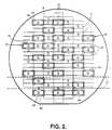
- indicium 14indicates the step in which a wafer 16 (see also FIG. 2) is tested by conventional methods to identify the locations on the wafer of good circuits 18 (also designated in FIG. 2 by indicium "G") and bad circuits 20. It is typical to dot the wafer where bad circuits are found, rather than to mark the good circuits with a "G" designation.
- a dicing schemeis defined for wafer 16 (step 22, FIG. 1), and defines locations 24 of oversized chips 25 which are to be diced from the wafer, as shown in FIG. 2. Dicing occurs preferably in two steps. First, the wafer is sawed, e.g., horizontally as shown by dashed lines 27, in such a manner as to avoid slicing through any oversized chip 25, and thus to separate the wafer into rows of chips 25, such as illustrated in FIG. 2. Then, each row is further sawed at a normal, i.e., vertically to the previously made horizontal saw lines 27, to form individual oversized chips 25.
- step 22In the dicing scheme of step 22 (FIG. 1), wherever possible to maximize use of the wafer material, locations 24 are selected to overlie bad circuits but, if necessary or unavoidable, over good circuits.
- step 26 of FIG. 1the good circuits are masked to protect their input/output pads and wafer 16 is passivated with an impervious, inorganic coating to provide the necessary hermeticity of the chip circuitry.
- dielectric materialis applied to the wafer (step 28 of FIG. 1). This dielectric material may comprise a thin overcoat of organic resin.
- a pattern of input/output relocation metalis then applied to the wafer to define leads 32, and thus to extend input/output pads 34 of each chip shown in FIG. 2. The performance of this step is noted in step 30 of FIG. 1.
- the processing of the wafervaries, depending upon whether the chips, which are to be diced from the wafer comprise lower or topmost chips.
- This variation in processingis represented as diverging processing steps for lower chips 36 and topmost chips 38.
- Those chips 38, which are intended to function as top chipsrequire two additional processing steps 40 and 42.
- ribbon bondable metalis applied to peripheral pads 34 (FIG. 2) and, as instructed in step 42, these pads are masked. If desired, wire leads may be used in place of ribbon leads, although the latter is preferred.
- the waferis passivated, followed by a dicing of the wafer into lower and topmost chips.
- step 52for each electric device, the lower chips and the topmost chip are stacked and bonded together into one of the assemblies illustrated in FIGS. 3-7.
- step 58for example, as it is understood in the art, the term “clear” refers to the step of removing passivation from interconnection pads, if the entire wafer has been passivated in step 46 prior to its being diced, and the term “metalize” refers to the application of suitable metallurgy to facilitate ribbon bonding, if necessary.
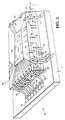
- assembly 62comprises a top chip 64 and lower chips 66 of equal planar dimensions.
- Top chip 64comprises one of chips 25 shown in FIG. 2 which has been processed according to steps 38, 40, 42, 46 and 50 of FIG. 1 so that it includes leads 32' and terminal pads 34'.
- Lower chips 66like top chip 64, comprise several of chips 25 of FIG. 2 which have been processed according to steps 36, 46 and 48 of FIG. 1 so that they include leads (not shown, but like leads 32 terminating in pads 34).
- All of chips 64 and 66after having been stacked and bonded together as subassembly 62, are ground at their respective edges 68 and on all sides on which connections are to be made, in order to ensure that all pads (e.g., pads 34' of topmost chip 64 and like pads on lower chips 66) are exposed and made flush in the planes of their respective sides, in accordance with step 54 of FIG. 1. Because it is desirable to increase the amount of metal of the exposed pads on lower chips 66, metalization 69 is added to these exposed pads. Interconnects 70 are then formed by conventional metalization techniques between or among selected pads (e.g., pads 34') and metalization 69 and, further, top pads 34' are metalized or cleared, as required by the electrical function, pursuant to steps 56 and 58.
- padse.g., pads 34' of topmost chip 64 and like pads on lower chips 66
- Stacked and bonded subassembly 62is then mounted on and affixed to a base 72, having pads 74, as required by step 76, and ribbon leads 78 are bonded respectively to pads 34' and to pads 74, as represented by step 80, to form an assembly 82.
- Assembly 82is then electrically tested according to step 84 to determine if its electrical function operates as intended. Should the test prove successful, assembly 82 is then mounted on and ribbon bonded to a fineline or other appropriate circuit board in accordance with steps 86 and 88. If the test is not successful, assembly 82 is returned for further processing or discarded, as appropriate. Successfully tested constructions are then encapsulated, if needed, as noted by step 90.
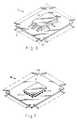
- a substrate circuit 100is provided with sufficient pads 102 to permit direct connection to the circuit of individual chips 104 which are stacked upon one another. No connections are made between the chips, but the chips can use selected pads in common on the substrate circuit.
- This techniquepermits a more conventional assembly to be made using existing processes, and does not require the development of new technologies or interconnecting chips on their vertical edges as shown in FIG. 3.
- one expedient methodis to mount chip 106 atop chip 108, and to interconnect upper chip 106 directly to lower chip 108 without the necessity of interconnections being made to a substrate as an intermediary circuit path.
- upper chip 106be smaller than lower chip 108, so as to provide room for pads on the lower chip to accommodate interconnecting wires or ribbons 110 from the upper chip.
- Assembly 94is then mounted and electrically coupled to a substrate (not shown) by groups of ribbon leads 112.
- FIG. 6it is possible also to mount several chips in a stack 114, like chips 104 shown in FIG. 4, where a group of upper chips 116 are smaller than chip 118 below, to permit accommodation of interconnecting pads on the lowest chip for all of the uppermost chips.
- the lowest chiphas pads at its periphery to permit its connection by ribbon leads 120 to a substrate (not shown).
- FIG. 7Yet another method is shown in FIG. 7 where an upper chip 122 is flip-chip mounted with bump pads 124 to a lower chip 126.
- the matched coefficient of thermal expansion of silicon on siliconcan be used to advantage.
Landscapes
- Engineering & Computer Science (AREA)
- Microelectronics & Electronic Packaging (AREA)
- Power Engineering (AREA)
- Physics & Mathematics (AREA)
- Condensed Matter Physics & Semiconductors (AREA)
- General Physics & Mathematics (AREA)
- Computer Hardware Design (AREA)
- Manufacturing & Machinery (AREA)
- Wire Bonding (AREA)
- Semiconductor Integrated Circuits (AREA)
- Dicing (AREA)
- Credit Cards Or The Like (AREA)
Description
Claims (11)
- A method for manufacture of a stacked chip assembly byfabricating, assembling and interconnecting at least twointegrated circuit or memory chips in a stacked upper (38;64; 104; 106; 116) and lower (36; 66; 104; 108; 118) chiparrangement (62) to a circuit substrate or printed wiringboard support (100) in such a manner that the planes of thechips are parallelly oriented to the substrate or wiringboard, comprising the steps of:testing (14) a full wafer (16) for determiningoperable (18) and inoperable (20) circuits therein;providing (22) a dicing scheme for defining oversizedchips (25) in which each wafer portion (24) which isselected to be formed into a chip (25) has a size that islarger than the individual circuit (18) which itincorporates, thus overlapping adjacent circuits (18; 20),and for positioning individual ones of said chips onselected ones of the operable circuits, thus overlappingsaid chips onto ones of the circuits adjacent the selectedcircuits, in preparation for dicing the wafer into theupper (38; 64; 104; 106; 116) and lower (36; 66; 104; 108;118) chips;applying (28) a dielectric layer mask to the wafer inaccordance with circuit designs defining the constituentparts of the stacked chip assembly;applying (30) input/output relocation metal toportions of the wafer exposed through the mask;for the top chip (38; 64; 104; 106; 116), applying(40) ribbon bondable metal to peripheral pads (34; 34') onthe wafer, and masking (42) the pads;passivating (46) the wafer;dicing (48) the wafer into the upper (38; 64; 104;106; 116) and lower (36; 66; 104; 108; 118) chips;assembling and bonding (52) the chips, one atop and incontact with an adjacent chip, into a layered stack (62;64, 66; 104; 106, 108; 116, 118) of chips;mounting (76) the stack (62; 64, 66; 104; 106, 108;116, 118) on a base (72);electrically bonding (80) the stack to the base by ribbon leads;electrically testing (84) the stacked and bondedchips;mounting (86) the stacked assembly (82; 92; 94; 96) tothe support;electrically bonding (88) the stacked assembly (82; 92; 94;96) to the support by ribbon leads ; andencapsulating (90) the stacked and bonded chips (62;64, 66; 104; 106, 108; 116, 118), base (72) and support(100) assembly.
- A method according to claim 1 further including thesteps (60), intermediate said steps of assembling andbonding (52) the chips (36; 38; 64; 66; 104; 106; 108; 116;118) into the stack (62; 64, 66; 104; 106, 108; 116, 118)and of mounting (76) the stack (62; 64, 66; 104; 106, 108;116, 118) on the base (72), of:grinding (54) edges (68) of the chips to exposeelectrical contact points (34);metallizing (56) the edges at selected ones of thecontact points (34);metallizing (58) selected ones of the pads (34') onthe uppermost chip (38; 64; 104; 106; 116); andperforming said stack to base electrically bonding step (80)by bonding ribbon leads (78; 112; 120) from the metallizededges and pads to designated contact areas on the base(72).
- A method according to claim 1 further comprising thestep of positioning contacts (34; 34') fully about theperiphery of each of the chips (36; 38; 64; 66; 104; 106;108; 116; 118).
- A method according to claim 1 in which the stackedchips (62; 64, 66; 104) have equal dimensions, furthercomprising the steps of electrically interconnecting thechips (64, 66; 104) at their edges and electricallyinterconnecting the uppermost chip (64; 104) and the base(72).
- A method according to claim 1 in which the stackedchips (62; 64, 66; 104) have equal dimensions, furthercomprising the step of electrically interconnecting thechips (64, 66; 104) to the base (72).
- A method according to claim 1 in which the stackedchips (106, 108; 116, 118) have unequal dimensions, furthercomprising the steps of stacking at least one of thosechips (106; 116) having lesser dimensions atop at leastanother of those chips (108; 118) having relatively largerdimensions, and electrically interconnecting the chipssuccessively to the lower chip and therefrom to the base.
- A method according to claim 1 further comprising thestep of forming interconnections (70; 110) among the chips(36; 38; 64; 66; 104; 106; 108; 116; 118) prior to saidchip to base interconnecting step (80).
- A method according to claim 7 wherein said chip tobase interconnecting step (80) comprises the step offorming connections (78) from an uppermost one (64; 104) ofthe chips to the base (72).
- An assembly of chips comprising at least twointegrated circuit chips stacked one (106; 114; 116) atopthe other (108; 116; 118), assembled parallelly on acircuit substrate (100) and electrically interconnected tosaid substrate,
each of said chips being of a size such that it comprises an operableindividual circuit (18)and adjacent circuits (18; 20) tosaid operable one,
characterized in that
said chips (106; 108; 114; 116; 118) areinterconnected by ribbon leads (112; 120) to said circuitsubstrate (100), and
said stacked chips (106; 108; 114; 116; 118) haveunequal dimensions, with at least one (106; 116) of thosechips having lesser dimensions (106; 114; 116) beingstacked atop at least another (108; 118) of those chips having relatively larger dimensions (108; 118), and furthercomprising ribbon leads between successive ones of saidupper chips to said lower chips and thence to saidsubstrate. - An assembly according to claim 9 further comprisingribbon leads extending from an uppermost one (106; 114) ofsaid chips to said circuit substrate (100).
- A method for manufacture of a stacked chip assembly byfabricating, assembling and interconnecting twointegrated circuit or memory chips in a stacked upper (38;122) and lower (36; 126) chip arrangement to a circuitsubstrate (100) or printed wiring board support in such amanner that the planes of the chips are parallelly orientedto the substrate or wiring board, comprising the steps of:testing (14) a full wafer (16) for determiningoperable (18) and inoperable (20) circuits therein;providing (22) a dicing scheme for defining oversizedchips (25) in which each wafer portion (24) which isselected to be formed into a chip (25) has a size that islarger than the individual circuit (18) which itincorporates, thus overlapping adjacent circuits (18; 20),and for positioning individual ones of said chips onselected ones of the operable circuits, thus overlappingsaid chips onto ones of the circuits adjacent the selectedcircuits, in preparation for dicing the wafer into theupper (38; 122) and lower (36; 126) chips;applying (28) a dielectric layer mask to the wafer inaccordance with circuit designs defining the constituentparts of the stacked chip assembly;applying (30) input/output relocation metal toportions of the wafer exposed through the mask;for the chip (126) to be the second chip from the topof a stack of chips, applying (40) ribbon bondable metal toperipheral pads (34; 34') on the wafer, and masking (42)the pads;passivating (46) the wafer;dicing (48) the wafer into the upper (38; 122) andlower (36; 126) chips; said upper chips being smaller than said lower chips;assembling and bonding (52) the chips, one atop and incontact with an adjacent chip, into a layered stack (122,126) of chips, the topmost chip (122) of the stack of chipsbeing flip-chip mounted with bump pads (124) to the chip(126) second from the top of the stack;mounting (76) the stack (122, 126) on a base (72);electrically bonding (80) the stack to the base by ribbon leads;electrically testing (84) the stacked and bondedchips;mounting (86) the stacked assembly (98) to thesupport;electrically bonding (88) the stacked assembly (98) to thesupport by ribbon leads; andencapsulating (90) the stacked and bonded chips (122,126), base (72) and support (100) assembly.
Applications Claiming Priority (2)
| Application Number | Priority Date | Filing Date | Title |
|---|---|---|---|
| US727500 | 1991-07-09 | ||
| US07/727,500US5311401A (en) | 1991-07-09 | 1991-07-09 | Stacked chip assembly and manufacturing method therefor |
Publications (3)
| Publication Number | Publication Date |
|---|---|
| EP0522518A2 EP0522518A2 (en) | 1993-01-13 |
| EP0522518A3 EP0522518A3 (en) | 1994-11-30 |
| EP0522518B1true EP0522518B1 (en) | 2002-05-22 |
Family
ID=24922916
Family Applications (1)
| Application Number | Title | Priority Date | Filing Date |
|---|---|---|---|
| EP92111531AExpired - LifetimeEP0522518B1 (en) | 1991-07-09 | 1992-07-08 | Stacked chip assembly and manufacturing method therefor |
Country Status (9)
| Country | Link |
|---|---|
| US (1) | US5311401A (en) |
| EP (1) | EP0522518B1 (en) |
| JP (1) | JPH0834283B2 (en) |
| KR (1) | KR960003768B1 (en) |
| AU (1) | AU656595B2 (en) |
| CA (1) | CA2073363A1 (en) |
| DE (1) | DE69232611T2 (en) |
| ES (1) | ES2173861T3 (en) |
| IL (1) | IL102397A (en) |
Families Citing this family (114)
| Publication number | Priority date | Publication date | Assignee | Title |
|---|---|---|---|---|
| FR2694840B1 (en)* | 1992-08-13 | 1994-09-09 | Commissariat Energie Atomique | Three-dimensional multi-chip module. |
| US6205654B1 (en)* | 1992-12-11 | 2001-03-27 | Staktek Group L.P. | Method of manufacturing a surface mount package |
| DE4311762C2 (en)* | 1993-04-08 | 1995-02-02 | Josef Dr Kemmer | Method of connecting electrical contact points |
| JP3354937B2 (en)* | 1993-04-23 | 2002-12-09 | イルビン センサーズ コーポレーション | An electronic module including a stack of IC chips each interacting with an IC chip fixed to the surface of the stack. |
| US5561622A (en)* | 1993-09-13 | 1996-10-01 | International Business Machines Corporation | Integrated memory cube structure |
| US6255726B1 (en)* | 1994-06-23 | 2001-07-03 | Cubic Memory, Inc. | Vertical interconnect process for silicon segments with dielectric isolation |
| US5675180A (en)* | 1994-06-23 | 1997-10-07 | Cubic Memory, Inc. | Vertical interconnect process for silicon segments |
| US6486528B1 (en) | 1994-06-23 | 2002-11-26 | Vertical Circuits, Inc. | Silicon segment programming apparatus and three terminal fuse configuration |
| US5657206A (en)* | 1994-06-23 | 1997-08-12 | Cubic Memory, Inc. | Conductive epoxy flip-chip package and method |
| US5891761A (en)* | 1994-06-23 | 1999-04-06 | Cubic Memory, Inc. | Method for forming vertical interconnect process for silicon segments with thermally conductive epoxy preform |
| US6124633A (en)* | 1994-06-23 | 2000-09-26 | Cubic Memory | Vertical interconnect process for silicon segments with thermally conductive epoxy preform |
| US5698895A (en)* | 1994-06-23 | 1997-12-16 | Cubic Memory, Inc. | Silicon segment programming method and apparatus |
| US6080596A (en)* | 1994-06-23 | 2000-06-27 | Cubic Memory Inc. | Method for forming vertical interconnect process for silicon segments with dielectric isolation |
| MY114888A (en)* | 1994-08-22 | 2003-02-28 | Ibm | Method for forming a monolithic electronic module by stacking planar arrays of integrated circuit chips |
| US5514907A (en)* | 1995-03-21 | 1996-05-07 | Simple Technology Incorporated | Apparatus for stacking semiconductor chips |
| US5612570A (en)* | 1995-04-13 | 1997-03-18 | Dense-Pac Microsystems, Inc. | Chip stack and method of making same |
| US5754408A (en)* | 1995-11-29 | 1998-05-19 | Mitsubishi Semiconductor America, Inc. | Stackable double-density integrated circuit assemblies |
| US6861290B1 (en)* | 1995-12-19 | 2005-03-01 | Micron Technology, Inc. | Flip-chip adaptor package for bare die |
| US5787569A (en)* | 1996-02-21 | 1998-08-04 | Lucent Technologies Inc. | Encapsulated package for power magnetic devices and method of manufacture therefor |
| US5815374A (en)* | 1996-09-30 | 1998-09-29 | International Business Machines Corporation | Method and apparatus for redirecting certain input/output connections of integrated circuit chip configurations |
| US5781413A (en)* | 1996-09-30 | 1998-07-14 | International Business Machines Corporation | Method and apparatus for directing the input/output connection of integrated circuit chip cube configurations |
| JP3462026B2 (en)* | 1997-01-10 | 2003-11-05 | 岩手東芝エレクトロニクス株式会社 | Method for manufacturing semiconductor device |
| JP2000031614A (en)* | 1997-11-04 | 2000-01-28 | Seiko Epson Corp | Memory module, laminate of memory modules, and memory card and computer including memory module |
| US6108210A (en)* | 1998-04-24 | 2000-08-22 | Amerasia International Technology, Inc. | Flip chip devices with flexible conductive adhesive |
| USRE43112E1 (en) | 1998-05-04 | 2012-01-17 | Round Rock Research, Llc | Stackable ball grid array package |
| US6072233A (en) | 1998-05-04 | 2000-06-06 | Micron Technology, Inc. | Stackable ball grid array package |
| US6121576A (en) | 1998-09-02 | 2000-09-19 | Micron Technology, Inc. | Method and process of contact to a heat softened solder ball array |
| IL143962A0 (en)* | 1999-01-08 | 2002-04-21 | Emisphere Tech Inc | Polymeric delivery agents and delivery agent compounds |
| US6313998B1 (en)* | 1999-04-02 | 2001-11-06 | Legacy Electronics, Inc. | Circuit board assembly having a three dimensional array of integrated circuit packages |
| US6323060B1 (en) | 1999-05-05 | 2001-11-27 | Dense-Pac Microsystems, Inc. | Stackable flex circuit IC package and method of making same |
| US6849480B1 (en) | 1999-05-07 | 2005-02-01 | Seagate Technology Llc | Surface mount IC stacking method and device |
| FR2794570B1 (en)* | 1999-06-04 | 2003-07-18 | Gemplus Card Int | METHOD FOR MANUFACTURING PORTABLE DEVICE WITH INTEGRATED CIRCUIT WITH ELECTRICAL CONDUCTION PATHS |
| US6572387B2 (en) | 1999-09-24 | 2003-06-03 | Staktek Group, L.P. | Flexible circuit connector for stacked chip module |
| US7102892B2 (en)* | 2000-03-13 | 2006-09-05 | Legacy Electronics, Inc. | Modular integrated circuit chip carrier |
| US6487078B2 (en) | 2000-03-13 | 2002-11-26 | Legacy Electronics, Inc. | Electronic module having a three dimensional array of carrier-mounted integrated circuit packages |
| US6713854B1 (en) | 2000-10-16 | 2004-03-30 | Legacy Electronics, Inc | Electronic circuit module with a carrier having a mounting pad array |
| NO20001360D0 (en)* | 2000-03-15 | 2000-03-15 | Thin Film Electronics Asa | Vertical electrical connections in stack |
| US6660561B2 (en) | 2000-06-15 | 2003-12-09 | Dpac Technologies Corp. | Method of assembling a stackable integrated circuit chip |
| US6404043B1 (en) | 2000-06-21 | 2002-06-11 | Dense-Pac Microsystems, Inc. | Panel stacking of BGA devices to form three-dimensional modules |
| JP2002033363A (en)* | 2000-07-19 | 2002-01-31 | Hitachi Ltd | Semiconductor wafer, semiconductor chip, and method of manufacturing semiconductor device |
| US6608763B1 (en) | 2000-09-15 | 2003-08-19 | Staktek Group L.P. | Stacking system and method |
| US7337522B2 (en)* | 2000-10-16 | 2008-03-04 | Legacy Electronics, Inc. | Method and apparatus for fabricating a circuit board with a three dimensional surface mounted array of semiconductor chips |
| US6885106B1 (en) | 2001-01-11 | 2005-04-26 | Tessera, Inc. | Stacked microelectronic assemblies and methods of making same |
| WO2002074024A2 (en)* | 2001-03-14 | 2002-09-19 | Legacy Electronics, Inc. | A method and apparatus for fabricating a circuit board with a three dimensional surface mounted array of semiconductor chips |
| US6462408B1 (en) | 2001-03-27 | 2002-10-08 | Staktek Group, L.P. | Contact member stacking system and method |
| US20030002267A1 (en)* | 2001-06-15 | 2003-01-02 | Mantz Frank E. | I/O interface structure |
| US6573460B2 (en)* | 2001-09-20 | 2003-06-03 | Dpac Technologies Corp | Post in ring interconnect using for 3-D stacking |
| US6573461B2 (en) | 2001-09-20 | 2003-06-03 | Dpac Technologies Corp | Retaining ring interconnect used for 3-D stacking |
| WO2003032370A2 (en)* | 2001-10-09 | 2003-04-17 | Tessera, Inc. | Stacked packages |
| US6977440B2 (en)* | 2001-10-09 | 2005-12-20 | Tessera, Inc. | Stacked packages |
| US7335995B2 (en)* | 2001-10-09 | 2008-02-26 | Tessera, Inc. | Microelectronic assembly having array including passive elements and interconnects |
| US7656678B2 (en) | 2001-10-26 | 2010-02-02 | Entorian Technologies, Lp | Stacked module systems |
| US6956284B2 (en) | 2001-10-26 | 2005-10-18 | Staktek Group L.P. | Integrated circuit stacking system and method |
| US7026708B2 (en) | 2001-10-26 | 2006-04-11 | Staktek Group L.P. | Low profile chip scale stacking system and method |
| US6940729B2 (en)* | 2001-10-26 | 2005-09-06 | Staktek Group L.P. | Integrated circuit stacking system and method |
| US7485951B2 (en) | 2001-10-26 | 2009-02-03 | Entorian Technologies, Lp | Modularized die stacking system and method |
| US7371609B2 (en) | 2001-10-26 | 2008-05-13 | Staktek Group L.P. | Stacked module systems and methods |
| US20030234443A1 (en)* | 2001-10-26 | 2003-12-25 | Staktek Group, L.P. | Low profile stacking system and method |
| US6576992B1 (en) | 2001-10-26 | 2003-06-10 | Staktek Group L.P. | Chip scale stacking system and method |
| US20050056921A1 (en)* | 2003-09-15 | 2005-03-17 | Staktek Group L.P. | Stacked module systems and methods |
| US6914324B2 (en)* | 2001-10-26 | 2005-07-05 | Staktek Group L.P. | Memory expansion and chip scale stacking system and method |
| US20050009234A1 (en)* | 2001-10-26 | 2005-01-13 | Staktek Group, L.P. | Stacked module systems and methods for CSP packages |
| US7053478B2 (en)* | 2001-10-26 | 2006-05-30 | Staktek Group L.P. | Pitch change and chip scale stacking system |
| US7202555B2 (en) | 2001-10-26 | 2007-04-10 | Staktek Group L.P. | Pitch change and chip scale stacking system and method |
| US7081373B2 (en) | 2001-12-14 | 2006-07-25 | Staktek Group, L.P. | CSP chip stack with flex circuit |
| US6765288B2 (en)* | 2002-08-05 | 2004-07-20 | Tessera, Inc. | Microelectronic adaptors, assemblies and methods |
| WO2004017399A1 (en)* | 2002-08-16 | 2004-02-26 | Tessera, Inc. | Microelectronic packages with self-aligning features |
| US7294928B2 (en)* | 2002-09-06 | 2007-11-13 | Tessera, Inc. | Components, methods and assemblies for stacked packages |
| US7071547B2 (en)* | 2002-09-11 | 2006-07-04 | Tessera, Inc. | Assemblies having stacked semiconductor chips and methods of making same |
| DE10250538B4 (en)* | 2002-10-29 | 2008-02-21 | Infineon Technologies Ag | Electronic component as multichip module and method for its production |
| US6856010B2 (en)* | 2002-12-05 | 2005-02-15 | Staktek Group L.P. | Thin scale outline package |
| US6841029B2 (en)* | 2003-03-27 | 2005-01-11 | Advanced Cardiovascular Systems, Inc. | Surface modification of expanded ultra high molecular weight polyethylene (eUHMWPE) for improved bondability |
| US20040207990A1 (en)* | 2003-04-21 | 2004-10-21 | Rose Andrew C. | Stair-step signal routing |
| US20040245615A1 (en)* | 2003-06-03 | 2004-12-09 | Staktek Group, L.P. | Point to point memory expansion system and method |
| US7061121B2 (en) | 2003-11-12 | 2006-06-13 | Tessera, Inc. | Stacked microelectronic assemblies with central contacts |
| US7705432B2 (en)* | 2004-04-13 | 2010-04-27 | Vertical Circuits, Inc. | Three dimensional six surface conformal die coating |
| US7245021B2 (en)* | 2004-04-13 | 2007-07-17 | Vertical Circuits, Inc. | Micropede stacked die component assembly |
| US7215018B2 (en)* | 2004-04-13 | 2007-05-08 | Vertical Circuits, Inc. | Stacked die BGA or LGA component assembly |
| JP4395166B2 (en) | 2004-06-07 | 2010-01-06 | 富士通マイクロエレクトロニクス株式会社 | Semiconductor device with built-in capacitor and manufacturing method thereof |
| US20060033187A1 (en)* | 2004-08-12 | 2006-02-16 | Staktek Group, L.P. | Rugged CSP module system and method |
| WO2006076381A2 (en)* | 2005-01-12 | 2006-07-20 | Legacy Electronics, Inc. | Radial circuit board, system, and methods |
| US7309914B2 (en)* | 2005-01-20 | 2007-12-18 | Staktek Group L.P. | Inverted CSP stacking system and method |
| US7033861B1 (en) | 2005-05-18 | 2006-04-25 | Staktek Group L.P. | Stacked module systems and method |
| US7576995B2 (en) | 2005-11-04 | 2009-08-18 | Entorian Technologies, Lp | Flex circuit apparatus and method for adding capacitance while conserving circuit board surface area |
| US7508069B2 (en) | 2006-01-11 | 2009-03-24 | Entorian Technologies, Lp | Managed memory component |
| US7508058B2 (en) | 2006-01-11 | 2009-03-24 | Entorian Technologies, Lp | Stacked integrated circuit module |
| US7608920B2 (en) | 2006-01-11 | 2009-10-27 | Entorian Technologies, Lp | Memory card and method for devising |
| US7605454B2 (en) | 2006-01-11 | 2009-10-20 | Entorian Technologies, Lp | Memory card and method for devising |
| US7304382B2 (en) | 2006-01-11 | 2007-12-04 | Staktek Group L.P. | Managed memory component |
| SG139573A1 (en) | 2006-07-17 | 2008-02-29 | Micron Technology Inc | Microelectronic packages with leadframes, including leadframes configured for stacked die packages, and associated systems and methods |
| US7545029B2 (en)* | 2006-08-18 | 2009-06-09 | Tessera, Inc. | Stack microelectronic assemblies |
| US7468553B2 (en) | 2006-10-20 | 2008-12-23 | Entorian Technologies, Lp | Stackable micropackages and stacked modules |
| US8723332B2 (en)* | 2007-06-11 | 2014-05-13 | Invensas Corporation | Electrically interconnected stacked die assemblies |
| TW200917391A (en)* | 2007-06-20 | 2009-04-16 | Vertical Circuits Inc | Three-dimensional circuitry formed on integrated circuit device using two-dimensional fabrication |
| US7763983B2 (en)* | 2007-07-02 | 2010-07-27 | Tessera, Inc. | Stackable microelectronic device carriers, stacked device carriers and methods of making the same |
| SG149726A1 (en) | 2007-07-24 | 2009-02-27 | Micron Technology Inc | Microelectronic die packages with metal leads, including metal leads for stacked die packages, and associated systems and methods |
| SG150396A1 (en)* | 2007-08-16 | 2009-03-30 | Micron Technology Inc | Microelectronic die packages with leadframes, including leadframe-based interposer for stacked die packages, and associated systems and methods |
| WO2009035849A2 (en) | 2007-09-10 | 2009-03-19 | Vertical Circuits, Inc. | Semiconductor die mount by conformal die coating |
| CN101999167B (en)* | 2008-03-12 | 2013-07-17 | 伊文萨思公司 | Support mounted electrically interconnected die assembly |
| US7863159B2 (en)* | 2008-06-19 | 2011-01-04 | Vertical Circuits, Inc. | Semiconductor die separation method |
| US9153517B2 (en) | 2008-05-20 | 2015-10-06 | Invensas Corporation | Electrical connector between die pad and z-interconnect for stacked die assemblies |
| FR2932004B1 (en)* | 2008-06-03 | 2011-08-05 | Commissariat Energie Atomique | STACKED ELECTRONIC DEVICE AND METHOD FOR PRODUCING SUCH AN ELECTRONIC DEVICE |
| WO2010151578A2 (en)* | 2009-06-26 | 2010-12-29 | Vertical Circuits, Inc. | Electrical interconnect for die stacked in zig-zag configuration |
| WO2011056668A2 (en) | 2009-10-27 | 2011-05-12 | Vertical Circuits, Inc. | Selective die electrical insulation additive process |
| TWI544604B (en) | 2009-11-04 | 2016-08-01 | 英維瑟斯公司 | Stacked die assembly having reduced stress electrical interconnects |
| FR2959350B1 (en) | 2010-04-26 | 2012-08-31 | Commissariat Energie Atomique | METHOD FOR MANUFACTURING A MICROELECTRONIC DEVICE AND MICROELECTRONIC DEVICE SO MANUFACTURED |
| MY166609A (en) | 2010-09-15 | 2018-07-17 | Semiconductor Components Ind Llc | Connector assembly and method of manufacture |
| US9490195B1 (en) | 2015-07-17 | 2016-11-08 | Invensas Corporation | Wafer-level flipped die stacks with leadframes or metal foil interconnects |
| US9871019B2 (en) | 2015-07-17 | 2018-01-16 | Invensas Corporation | Flipped die stack assemblies with leadframe interconnects |
| US9825002B2 (en) | 2015-07-17 | 2017-11-21 | Invensas Corporation | Flipped die stack |
| US9508691B1 (en) | 2015-12-16 | 2016-11-29 | Invensas Corporation | Flipped die stacks with multiple rows of leadframe interconnects |
| US10566310B2 (en) | 2016-04-11 | 2020-02-18 | Invensas Corporation | Microelectronic packages having stacked die and wire bond interconnects |
| US9595511B1 (en) | 2016-05-12 | 2017-03-14 | Invensas Corporation | Microelectronic packages and assemblies with improved flyby signaling operation |
| US9728524B1 (en) | 2016-06-30 | 2017-08-08 | Invensas Corporation | Enhanced density assembly having microelectronic packages mounted at substantial angle to board |
Family Cites Families (9)
| Publication number | Priority date | Publication date | Assignee | Title |
|---|---|---|---|---|
| US456743A (en)* | 1891-07-28 | Charles e | ||
| WO1985002060A1 (en)* | 1983-10-24 | 1985-05-09 | Sintra-Alcatel, S.A. | Method for substituting an electronic component connected to the conductor tracks of a carrier substrate |
| JPS60130854A (en)* | 1983-12-20 | 1985-07-12 | Toshiba Corp | Semiconductor integrated circuit |
| JPS6118164A (en)* | 1984-07-04 | 1986-01-27 | Mitsubishi Electric Corp | semiconductor equipment |
| US4954875A (en)* | 1986-07-17 | 1990-09-04 | Laser Dynamics, Inc. | Semiconductor wafer array with electrically conductive compliant material |
| JPH01140652A (en)* | 1987-11-26 | 1989-06-01 | Sharp Corp | Three-dimensional semiconductor device |
| JPH0750759B2 (en)* | 1988-07-01 | 1995-05-31 | シャープ株式会社 | Semiconductor device |
| US4996583A (en)* | 1989-02-15 | 1991-02-26 | Matsushita Electric Industrial Co., Ltd. | Stack type semiconductor package |
| WO1991000683A2 (en)* | 1989-07-07 | 1991-01-24 | Irvine Sensors Corporation | Fabricating electronic circuitry unit containing stacked ic layers having lead rerouting |
- 1991
- 1991-07-09USUS07/727,500patent/US5311401A/ennot_activeExpired - Fee Related
- 1992
- 1992-07-02ILIL10239792Apatent/IL102397A/ennot_activeIP Right Cessation
- 1992-07-06AUAU19475/92Apatent/AU656595B2/ennot_activeCeased
- 1992-07-08ESES92111531Tpatent/ES2173861T3/ennot_activeExpired - Lifetime
- 1992-07-08KRKR1019920012113Apatent/KR960003768B1/ennot_activeExpired - Fee Related
- 1992-07-08DEDE69232611Tpatent/DE69232611T2/ennot_activeExpired - Fee Related
- 1992-07-08CACA002073363Apatent/CA2073363A1/ennot_activeAbandoned
- 1992-07-08EPEP92111531Apatent/EP0522518B1/ennot_activeExpired - Lifetime
- 1992-07-09JPJP4204302Apatent/JPH0834283B2/ennot_activeExpired - Fee Related
Also Published As
| Publication number | Publication date |
|---|---|
| JPH05259375A (en) | 1993-10-08 |
| KR960003768B1 (en) | 1996-03-22 |
| DE69232611T2 (en) | 2003-01-30 |
| ES2173861T3 (en) | 2002-11-01 |
| IL102397A0 (en) | 1993-05-13 |
| JPH0834283B2 (en) | 1996-03-29 |
| CA2073363A1 (en) | 1993-01-10 |
| KR930003308A (en) | 1993-02-24 |
| IL102397A (en) | 1995-03-30 |
| DE69232611D1 (en) | 2002-06-27 |
| EP0522518A2 (en) | 1993-01-13 |
| EP0522518A3 (en) | 1994-11-30 |
| AU1947592A (en) | 1993-01-21 |
| AU656595B2 (en) | 1995-02-09 |
| US5311401A (en) | 1994-05-10 |
Similar Documents
| Publication | Publication Date | Title |
|---|---|---|
| EP0522518B1 (en) | Stacked chip assembly and manufacturing method therefor | |
| US7115441B2 (en) | Semiconductor package with semiconductor chips stacked therein and method of making the package | |
| US7545048B2 (en) | Stacked die package | |
| US5886412A (en) | Angularly offset and recessed stacked die multichip device | |
| US5126286A (en) | Method of manufacturing edge connected semiconductor die | |
| US6818998B2 (en) | Stacked chip package having upper chip provided with trenches and method of manufacturing the same | |
| US6461897B2 (en) | Multichip module having a stacked chip arrangement | |
| US7074696B1 (en) | Semiconductor circuit module and method for fabricating semiconductor circuit modules | |
| US6873040B2 (en) | Semiconductor packages for enhanced number of terminals, speed and power performance | |
| US20030164543A1 (en) | Interposer configured to reduce the profiles of semiconductor device assemblies and packages including the same and methods | |
| US20070252262A1 (en) | Die Assembly Having Electrical Interconnect | |
| US20020047214A1 (en) | Multi-chip package-type semiconductor device | |
| JPS6355213B2 (en) | ||
| JP2001257310A (en) | Semiconductor device and method of manufacturing therefor, and testing method for the same | |
| EP0729645B1 (en) | A high density integrated circuit assembly combining leadframe leads with conductive traces | |
| US6888222B2 (en) | Semiconductor device | |
| US6246124B1 (en) | Encapsulated chip module and method of making same | |
| JP3529050B2 (en) | Method for manufacturing semiconductor device | |
| KR100207902B1 (en) | Multi chip package using lead frame | |
| US20040089930A1 (en) | Simplified stacked chip assemblies | |
| KR100532948B1 (en) | method for manufacturing ball grid array type package | |
| KR20020085954A (en) | stack package and method of fabricating the same | |
| KR20030016855A (en) | Stacked chip scale package |
Legal Events
| Date | Code | Title | Description |
|---|---|---|---|
| PUAI | Public reference made under article 153(3) epc to a published international application that has entered the european phase | Free format text:ORIGINAL CODE: 0009012 | |
| AK | Designated contracting states | Kind code of ref document:A2 Designated state(s):CH DE ES FR GB IT LI SE | |
| PUAL | Search report despatched | Free format text:ORIGINAL CODE: 0009013 | |
| RHK1 | Main classification (correction) | Ipc:H01L 25/065 | |
| AK | Designated contracting states | Kind code of ref document:A3 Designated state(s):CH DE ES FR GB IT LI SE | |
| 17P | Request for examination filed | Effective date:19950529 | |
| 17Q | First examination report despatched | Effective date:19970417 | |
| RAP1 | Party data changed (applicant data changed or rights of an application transferred) | Owner name:RAYTHEON COMPANY | |
| GRAG | Despatch of communication of intention to grant | Free format text:ORIGINAL CODE: EPIDOS AGRA | |
| GRAG | Despatch of communication of intention to grant | Free format text:ORIGINAL CODE: EPIDOS AGRA | |
| GRAH | Despatch of communication of intention to grant a patent | Free format text:ORIGINAL CODE: EPIDOS IGRA | |
| GRAH | Despatch of communication of intention to grant a patent | Free format text:ORIGINAL CODE: EPIDOS IGRA | |
| GRAA | (expected) grant | Free format text:ORIGINAL CODE: 0009210 | |
| REG | Reference to a national code | Ref country code:GB Ref legal event code:FG4D | |
| REG | Reference to a national code | Ref country code:CH Ref legal event code:EP | |
| REG | Reference to a national code | Ref country code:CH Ref legal event code:NV Representative=s name:ISLER & PEDRAZZINI AG | |
| REF | Corresponds to: | Ref document number:69232611 Country of ref document:DE Date of ref document:20020627 | |
| ET | Fr: translation filed | ||
| REG | Reference to a national code | Ref country code:ES Ref legal event code:FG2A Ref document number:2173861 Country of ref document:ES Kind code of ref document:T3 | |
| PLBE | No opposition filed within time limit | Free format text:ORIGINAL CODE: 0009261 | |
| STAA | Information on the status of an ep patent application or granted ep patent | Free format text:STATUS: NO OPPOSITION FILED WITHIN TIME LIMIT | |
| 26N | No opposition filed | Effective date:20030225 | |
| PGFP | Annual fee paid to national office [announced via postgrant information from national office to epo] | Ref country code:FR Payment date:20050614 Year of fee payment:14 | |
| PGFP | Annual fee paid to national office [announced via postgrant information from national office to epo] | Ref country code:GB Payment date:20050615 Year of fee payment:14 | |
| PGFP | Annual fee paid to national office [announced via postgrant information from national office to epo] | Ref country code:DE Payment date:20050617 Year of fee payment:14 | |
| PGFP | Annual fee paid to national office [announced via postgrant information from national office to epo] | Ref country code:CH Payment date:20050620 Year of fee payment:14 | |
| PGFP | Annual fee paid to national office [announced via postgrant information from national office to epo] | Ref country code:SE Payment date:20050622 Year of fee payment:14 | |
| PGFP | Annual fee paid to national office [announced via postgrant information from national office to epo] | Ref country code:ES Payment date:20050705 Year of fee payment:14 | |
| PG25 | Lapsed in a contracting state [announced via postgrant information from national office to epo] | Ref country code:GB Free format text:LAPSE BECAUSE OF NON-PAYMENT OF DUE FEES Effective date:20060708 | |
| PG25 | Lapsed in a contracting state [announced via postgrant information from national office to epo] | Ref country code:SE Free format text:LAPSE BECAUSE OF NON-PAYMENT OF DUE FEES Effective date:20060709 | |
| PG25 | Lapsed in a contracting state [announced via postgrant information from national office to epo] | Ref country code:LI Free format text:LAPSE BECAUSE OF NON-PAYMENT OF DUE FEES Effective date:20060731 Ref country code:CH Free format text:LAPSE BECAUSE OF NON-PAYMENT OF DUE FEES Effective date:20060731 | |
| PGFP | Annual fee paid to national office [announced via postgrant information from national office to epo] | Ref country code:IT Payment date:20060731 Year of fee payment:15 | |
| PG25 | Lapsed in a contracting state [announced via postgrant information from national office to epo] | Ref country code:DE Free format text:LAPSE BECAUSE OF NON-PAYMENT OF DUE FEES Effective date:20070201 | |
| REG | Reference to a national code | Ref country code:CH Ref legal event code:PL | |
| EUG | Se: european patent has lapsed | ||
| GBPC | Gb: european patent ceased through non-payment of renewal fee | Effective date:20060708 | |
| REG | Reference to a national code | Ref country code:FR Ref legal event code:ST Effective date:20070330 | |
| REG | Reference to a national code | Ref country code:ES Ref legal event code:FD2A Effective date:20060710 | |
| PG25 | Lapsed in a contracting state [announced via postgrant information from national office to epo] | Ref country code:ES Free format text:LAPSE BECAUSE OF NON-PAYMENT OF DUE FEES Effective date:20060710 | |
| PG25 | Lapsed in a contracting state [announced via postgrant information from national office to epo] | Ref country code:FR Free format text:LAPSE BECAUSE OF NON-PAYMENT OF DUE FEES Effective date:20060731 | |
| PG25 | Lapsed in a contracting state [announced via postgrant information from national office to epo] | Ref country code:IT Free format text:LAPSE BECAUSE OF NON-PAYMENT OF DUE FEES Effective date:20070708 |