EP0516064B1 - Integrated optical modulator and method of providing a linearly modulated light signal - Google Patents
Integrated optical modulator and method of providing a linearly modulated light signalDownload PDFInfo
- Publication number
- EP0516064B1 EP0516064B1EP92108878AEP92108878AEP0516064B1EP 0516064 B1EP0516064 B1EP 0516064B1EP 92108878 AEP92108878 AEP 92108878AEP 92108878 AEP92108878 AEP 92108878AEP 0516064 B1EP0516064 B1EP 0516064B1
- Authority
- EP
- European Patent Office
- Prior art keywords
- modulator
- interferometric
- modulators
- type
- coupler
- Prior art date
- Legal status (The legal status is an assumption and is not a legal conclusion. Google has not performed a legal analysis and makes no representation as to the accuracy of the status listed.)
- Expired - Lifetime
Links
Images


Classifications
- G—PHYSICS
- G02—OPTICS
- G02F—OPTICAL DEVICES OR ARRANGEMENTS FOR THE CONTROL OF LIGHT BY MODIFICATION OF THE OPTICAL PROPERTIES OF THE MEDIA OF THE ELEMENTS INVOLVED THEREIN; NON-LINEAR OPTICS; FREQUENCY-CHANGING OF LIGHT; OPTICAL LOGIC ELEMENTS; OPTICAL ANALOGUE/DIGITAL CONVERTERS
- G02F1/00—Devices or arrangements for the control of the intensity, colour, phase, polarisation or direction of light arriving from an independent light source, e.g. switching, gating or modulating; Non-linear optics
- G02F1/01—Devices or arrangements for the control of the intensity, colour, phase, polarisation or direction of light arriving from an independent light source, e.g. switching, gating or modulating; Non-linear optics for the control of the intensity, phase, polarisation or colour
- G02F1/21—Devices or arrangements for the control of the intensity, colour, phase, polarisation or direction of light arriving from an independent light source, e.g. switching, gating or modulating; Non-linear optics for the control of the intensity, phase, polarisation or colour by interference
- G02F1/225—Devices or arrangements for the control of the intensity, colour, phase, polarisation or direction of light arriving from an independent light source, e.g. switching, gating or modulating; Non-linear optics for the control of the intensity, phase, polarisation or colour by interference in an optical waveguide structure
- G—PHYSICS
- G02—OPTICS
- G02F—OPTICAL DEVICES OR ARRANGEMENTS FOR THE CONTROL OF LIGHT BY MODIFICATION OF THE OPTICAL PROPERTIES OF THE MEDIA OF THE ELEMENTS INVOLVED THEREIN; NON-LINEAR OPTICS; FREQUENCY-CHANGING OF LIGHT; OPTICAL LOGIC ELEMENTS; OPTICAL ANALOGUE/DIGITAL CONVERTERS
- G02F1/00—Devices or arrangements for the control of the intensity, colour, phase, polarisation or direction of light arriving from an independent light source, e.g. switching, gating or modulating; Non-linear optics
- G02F1/29—Devices or arrangements for the control of the intensity, colour, phase, polarisation or direction of light arriving from an independent light source, e.g. switching, gating or modulating; Non-linear optics for the control of the position or the direction of light beams, i.e. deflection
- G02F1/31—Digital deflection, i.e. optical switching
- G02F1/313—Digital deflection, i.e. optical switching in an optical waveguide structure
- G02F1/3136—Digital deflection, i.e. optical switching in an optical waveguide structure of interferometric switch type
- G—PHYSICS
- G02—OPTICS
- G02F—OPTICAL DEVICES OR ARRANGEMENTS FOR THE CONTROL OF LIGHT BY MODIFICATION OF THE OPTICAL PROPERTIES OF THE MEDIA OF THE ELEMENTS INVOLVED THEREIN; NON-LINEAR OPTICS; FREQUENCY-CHANGING OF LIGHT; OPTICAL LOGIC ELEMENTS; OPTICAL ANALOGUE/DIGITAL CONVERTERS
- G02F2203/00—Function characteristic
- G02F2203/19—Function characteristic linearised modulation; reduction of harmonic distortions
Definitions
- This inventionrelates generally to modulators, and more particularly to integrated electro-optical modulators and a method of providing a linearly modulated light signal.
- Integrated electro-optical modulatorsare finding increasing use in state-of-the-art analog optical-fiber communication systems. Such systems are being developed as an alternative to conventional electromagnetic transmission lines.
- Present optical-fiber communication systemsmay consist of a high power, low noise laser source in conjunction with a wide bandwidth external modulator, for example.
- a common problem in such systemsis that the dynamic range thereof is limited by intermodulation distortion, and by harmonic distortion due to modulator nonlinearities. Many attempts have been made in the art to improve the linearity of the modulators.
- One method of improving the linearity of optical modulatorsis to provide electromagnetic predistortion of the input signal.
- a system for accomplishing thisis reported in an article by R.P. Childs and D.A. O'Byrne, that appeared in OFC 90, entitled "Predistortion Linearization of Directly Modulated DFB Lasers and External Modulators for AM Video Transmission.”
- Johnson U.S. Patents 5,015,053 and 5,002,355refer to linearization of an interferometric modulator by coupling to transverse electric (TE) and transverse magnetic (TM) modes.
- a carrier wave derived from a light sourceis polarized by a polarizer for adjusting the power of the carrier wave in the TE and TM polarization modes.
- Hamilton et al. U.S. Patent 5,010,346shows an electro-optical analog-to-digital converter.
- a laser light sourceis synchronized with a digital clock for producing pulses of light.
- the pulses of lightare modulated by an optical modulator for varying the intensity of the pulses of light as a function of the amplitude of the analog modulating signal.
- the light pulsesare demultiplexed and passed through a detector for converting the light pulses to electrical signals.
- the electrical signalsare then passed through an electrical analog-to-digital converter.
- DuPuy et al U.S. Patent 4,997,245shows optical switches that are polarization independent.
- the optical switchesinclude a substrate of electro-optic material in which waveguides are formed in a manner permitting light waves to be switched therethrough independent of polarization phenomena.
- Thylen U.S. Patent 4,993,798refers to an optical communication system consisting of a semiconductor laser that includes an optical waveguide coupled at one end to first and second optical directional switches. The other ends of each one of the directional couplers each have an end of a waveguide terminated to a mirror, for forming a cavity including the laser diode. By either modulating current driving the diode, or by applying a modulating signal to the directional couplers, a light signal passing therethrough can be modulated.
- Yoon et al U.S. Patent 4,936,645shows a polarization-insensitive Mach-Zehnder modulator that includes a thin film waveguide on a substrate.
- the modulatorconsists of a lamination of different organic polymers upon which the thin film waveguide is deposited, and electrodes for applying voltages for producing electric fields to coact with the light passing through the waveguides.
- Koai U.S. Patent 4,934,776teaches the combination of cascaded individual waveguide directional coupler sections arranged to provide a high-density optical data array, for forming an integrated optical intensity modulator.
- the cascaded coupled-waveguide modulatorsprovide ultra-high extinction ratios.
- Koai U.S. Patent 4,934,775shows an optical space-division switching architecture consisting of high-extinction electro-optical data arrays of a plurality of cascaded coupled-waveguide optical intensity modulators.
- a plurality of passive splitter circuitsare used to evenly divide an input optical signal into a plurality of interim optical signals.
- the optical signalsare passed through the optical intensity modulators, respectively, which have waveguide coupler sections cascaded together on a crystal substrate to form a bar-type modulator structure, for providing a direct optical connection between the various sections of each modulator.
- Combiner circuitsreceive the output optical signals from the data arrays and combine them for providing a single output wave or signal.
- Coleman U.S. Patent 4,882,775shows a demodulator provided by a an interferometer and a signal processor.
- the demodulatoris included in a coherence multiplexed, optical data transmission system.
- the optical data transmission systemincludes an interferometric modulator at an input end.
- the output signals therefromare modulated waveforms which are passed through an optical multiplexer, and coupled via single mode optical couplers and a fiber optic cable to demodulator stages.
- Each modulator and demodulator stageis provided by an unequal arm-length Mach-Zehnder interferometer.
- the multiplexersphase modulate the optical carriers from the modulators for multiplexing the same together.
- the path lengths between the modulators and demodulators included in the systemare controlled for obtaining a desired output from the output demodulator stages 40.
- U.S. Patent 4,390,236shows an electro-optical demultiplexer consisting of a plurality of cascaded tunable, polarization independent optical wavelength filters.
- the various sections of the filters, as cascaded,provide an input polarization selective coupler that separates the transverse electrical (TE) and transverse magnetic (TM) orthogonally polarized wave components, respectively, of an arbitrarily polarized input signal.
- the separated TE and TM componentsthen travel along two different wavepaths or waveguides.
- Each waveguideincludes a wavelength selective mode converter.
- An output polarization selective coupleris provided for combining in one output waveguide signal components centered about the wavelength of the mode converters, and for combining in a second output waveguide the balance of the input signal.
- Papuchon U.S. Patent 4,223,977shows an integrated optical circuit for separating a plurality of optical waves of different wavelengths, thereby providing a demultiplexing function.
- a plurality of basic electro-optical cellsare integrated on a single substrate for providing the optical demultiplexing circuit.
- a paper entitled "Waveguide Modulators with Extended Linear Dynamic Range a Theoretical Prediction”shows a modified-directional-coupler modulator with reduced nonlinear distortion.
- the couplerincludes an input stage for receiving input signals for a voltage control directional coupler that couples the signals to a Mach-Zehnder interferometer.
- the output of the interferometeris coupled by a fixed directional coupler to an output waveguide providing two channels. The parameters are adjusted for minimizing third order intermodulation spurious signals.
- a paper entitled "In Search of a Linear Electro-optic Amplitude Modulator"shows a linear electro-optic amplitude modulator.
- the modulatorincludes a Y-branch for dividing an optical input signal equally for inputting into the two arms, respectively, of a Mach-Zehnder interferometer.
- the interferometerfunctions as a phase shifter.
- the output of the interferometeris supplied to a directional coupler having a nominal coupling constant-length product of half a coupling length.
- the optical output signalis provided at each of two output waveguides.
- a modulation signal of one polarityis applied to the interferometer phase shifter, and is applied in reverse polarity to the directional coupler using a multiplication factor.
- the parametersare adjusted for optimizing the linearity of the modulator by reducing the second and third order harmonics that cause nonlinearities to occur.
- the present inventorrecognized that known integrated optics modulators require further improvement.
- One need recognizedis to improve the linearity of integrated optical modulators.
- An object of the present inventionis to provide an improved integrated optical modulator.
- Another object of the inventionis to provide an integrated optical modulator having increased linearity.
- an integrated optical modulatorhaving a plurality of cascaded stages of Mach-Zehnder type Y-branch configured interferometric modulators and coupler structure interferometric modulators.
- the amplitude of the modulating voltage applied to each stage, and the level of the DC bias applied to each stage,are adjusted for increasing the linearity of the modulated output signal.
- various ones of the stagesmay each be provided by a 2X1 interferometric switch.
- a Y-branch electro-optical interferometric modulator 2is shown.
- An input light wave P 0typically having a power level expressed in milliwatts, is applied to an input waveguide 4, for carrying the light wave P o to be divided into upper waveguide segment 6 and lower waveguide segment 8 of the Y-waveguide 4, 6, 8.
- Light from the upper segment 6travels through a longitudinal upper waveguide segment 10, through an upper waveguide segment 12, and through an output waveguide segment 14 for providing a portion of an output light signal P (t) .
- a lower leg or waveguide segment 16forms a Y-branch with waveguide segments 14 and 16.
- Waveguide segment 16receives light from a lower longitudinal waveguide segment 18 at one end thereof, the other end of the latter being connected to receive light from an end of the lower waveguide segment 8.
- waveguide segments 4, 6, 10, 12 and 14form a continuous waveguide, as do waveguide segments 4, 8, 18, 16 and 14.
- An elongated relatively narrow metal electrode 20is positioned relatively close to the top of the upper longitudinal waveguide segment 10, with the longitudinal axis of each being parallel.
- Another electrode 22that is rectangular in shape, but substantially wider than electrode 20, in this example, is located between the upper and lower longitudinal waveguide segments 10 and 18 with its longitudinal axis parallel thereto.
- a third electrode 24 substantially identical in shape to electrode 20is located beneath waveguide segment 18, with the longitudinal axes of the two being parallel. Electrode 24 has substantially the same shape as electrode 20, with these electrodes and electrode 22 all being juxtaposed and in vertical alignment with one another, in this example.
- a modulating or instantaneous voltage V(t)is connected to electrode 22.
- the upper and lower electrodes 20 and 24are each connected to a source of reference potential, ground in this example.
- a DC bias voltage ⁇ 1is also connected to electrode 22.
- Electrodes 20, 22, and 24are deposited on top of the substrate 82. Note that the shape of any of the electrodes illustrated above are not meant to be limiting in that many shapes or configurations can be used for the electrodes.
- a light signal P 0 applied to input waveguide 4is substantially equally divided. One half portion travels through waveguide segments 6, 10, 12, and another half portion travels through waveguide segments 8, 16, and 18, as indicated above.
- Light traveling through waveguide segment 10passes between electrodes 20 and 22, and the light through waveguide segment 18 passes between electrodes 22 and 24.
- the modulating signal V(t)causes the index of refraction of the crystal substrate 82 to change for increasing the speed of light through waveguide 10, and decreasing the speed of light through waveguide 18, for example, in accordance with the instantaneous amplitude at any given time of the modulating signal V(t).
- the phase difference created between the light traveling through the upper waveguide 10 and lower waveguide 18modulates the light.
- the light from waveguide 10then travels through waveguide 12 to output waveguide 14, and light from waveguide 18 through waveguide 16 to waveguide 14, whereby the two portions of the original light signal P 0 are combined together to form the modulated output light signal P (t) .
- the output light signal P (t)includes only the in-phase components of the modulated light, in that in a Y-branch modulator components of light that are in phase quadrature are absorbed in the crystal substrate 82, in this example.
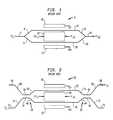
- FIG. 2Another known interferometric coupler structure for providing a Mach-Zehnder interferometric modulator 26 is shown in Fig. 2.
- the formerincludes waveguide coupling sections 28 and 30.
- a light wave P 0 signalis delivered to a lower input waveguide segment 32 that lies relatively in a substantially horizontal plane, with the light being conducted therefrom through an upward sloping waveguide segment 34, and therefrom through a lower horizontal waveguide segment 36 of a coupling section 28.
- a portion of the light traveling through the lower horizontal waveguide segment 36ideally has half of its light energy coupled into the upper horizontal waveguide portion 38 of coupler 28.
- the remaining light from waveguide 36then travels through the downward sloping waveguide section or segment 40, therefrom through the lower longitudinal waveguide segment 42, then through an upwardly sloping waveguide segment 44 and into a horizontal lower waveguide segment 46 of a second coupler 30.
- the latteralso includes an upper horizontal waveguide segment 48.
- Light coupled from lower horizontal waveguide segment 36 of coupler 28, coupled into the upper horizontal segment 38travels from the latter to an upwardly sloping waveguide segment 50, through an upper longitudinal waveguide segment 52, into a downwardly sloping waveguide segment 54, and therefrom into the upper horizontal waveguide segment 48 of coupler 46, where this light is combined with light coupled thereinto from the lower horizontal waveguide segment 46 of this coupler.
- Both the linear and nonlinear components of the light wave signals combined in waveguide segment 48travel therefrom through an upwardly sloping waveguide segment 56 to a horizontal waveguide segment 58, for outputting therefrom as an output light signal P (t) , in this example.
- a relatively narrow rectangular electrode 60is positioned above the upper longitudinal waveguide segment 52, and a similar electrode 62 is positioned below lower longitudinal waveguide segment 42.
- a third electrode 64that is substantially wider than either of electrodes 60 and 62, in this example, is positioned between the upper and lower longitudinal waveguides 52, 42, respectively.
- the electrodes 60, 62, and 64are juxtaposed and substantially in alignment with one another.
- the lower waveguide segment 32has a corresponding upper waveguide segment 66 that continues into a downwardly sloping upper waveguide segment 68.
- the upper output waveguide segment 58has a corresponding lower waveguide segment 70, with the latter connecting with a downward sloping lower waveguide segment 72, as shown.
- the electrodescan have other configurations than those illustrated herein.
- the operation of the coupler structure interferometric modulator 26is similar to that of the Y-branch interferometric modulator 2 of Fig. 1. However, unlike the latter which absorbs the phase quadrature components of the output wave form in the crystal substrate 82, the coupler structure modulator 26 does not absorb these phase quadrature components. Therefore, the coupler interferometric modulator 26 tends to provide a higher output light signal P (t) .
- the transfer function for the coupler structure interferometric modulator 26can be the same as the Y-branch interferometric modulator 2, as given in equation (1) above.
- Equator 2 and modulator 26are configured for each having the transfer function of equation (1).
- ⁇ (t)is also representative of the phase difference between the two light signals modulated as described in either one of the modulators 2 and 26. Accordingly, the nonlinearity of either the modulators 2 or 26 can be described by approximating equation 1 as shown below in equation (3): (3) P (t) ⁇ Po/2 [1 + cos ⁇ - sin ⁇ . ⁇ (t) - 1/2 cos ⁇ . ⁇ 2 (t) + 1/6 sin ⁇ .
- the present inventorrecognized that compensation for nonlinearities due to second, third, and higher order harmonics can be obtained when suitable combinations of the transfer functions of equations 1 and 2 are implemented.
- the present inventionprovides such suitable combinations of these transfer functions by cascade coupling two or more interferometric modulators such as some combination of modulators 2 and 26 of Figs.
- n2, 3, 4.
- a first stageis a Y-branch interferometric modulator 2
- a second stageis a coupler-structure interferometric modulator 26, as shown in Fig. 3.
- Fig. 3In another embodiment of the invention, as shown in Fig.
- the first stage or input stageis also a Y-branch interferometric modulator 2
- the second or output stageis shown as 2X1 switch or interferometric modulator 73 that includes a coupler input section 74 and a Y-branch output section 76, instead of a coupler output section 30 as in interferometric modulator 26.
- a linearized interferometric modulatorcan be provided by cascading some combination of a plurality of the modulator configurations 2, 26, and 73, or 2 and 26, or 2 and 73, or 26 and 73, or all of one type, for example.
- a simplified pictorial illustrationis shown of a two-stage cascaded integrated optical modulator 80 that includes a substrate 82 of lithium niobate crystal, for example.
- Interferometric modulatorssubstantially similar to modulators 2 and 26 of Fig. 3 are formed in cascade on the substrate.
- the only difference between the configurations of modulators 2 and 26 shown in Fig. 5, and those of Fig. 3,is that in Fig. 5 the electrodes 20, 22, and 24 are more practically shown for modulator 2, with similar comments applying for the electrodes 60, 62, and 64 of modulator 26.
- a substantially U-shaped electrode 84provides electrode 24 at its base, and electrode 20 in two inwardly projecting segments from the upper portions of arms 86 and 88.
- the ends of arms 86 and 88terminate to connector or terminal pads 90 and 92 for connection via conductors 94 and 96, respectively, to ground pads 98 and 100 of an auxiliary printed circuit (PC) board 102, as shown.
- the U-shaped electrode 84is formed on top of the substrate 82 over the waveguide segments 6, 8, 12, and 16, as shown.
- Center electrode 22is formed by a shortened T-like electrode configuration having a terminal pad 102 for connection via a conductor 104 to a conductor 106 on PC board 102, for receiving an input voltage signal V(t), and a DC bias voltage ⁇ 1 , in this example.
- a fiber optic cable 108is coupled via a fiber cable-to-substrate attachment 110 to an end of input waveguide segment 4 of modulator 2, for delivering a light signal thereto.
- the electrodes for modulator 26are provided from a relatively U-shaped electrode 112 formed on top of the substrate 82 as shown, for providing electrode 62 at its base, and electrodes 60 from stub-like inwardly projecting electrode portions from the upper ends of the electrode arms 114 and 116.
- the ends of arms 114 and 116terminate to connecting pads 118 and 120, respectively, for connection via conductors 122 and 124 to ground pads 126 and 128 formed on PC board 102 as shown.
- the center electrode 64is formed on top of the substrate 82 in a substantially stub-like T-configuration, as shown, where the leg of the T-configuration terminates to a connection pad 130 for connection via a conductor 132 to an end of conductor strip 134 on PC board 102, for receiving an input signal k V(t) and a DC bias ⁇ 2 .
- a light fiber cable 136is connected via a fiber cable-to-substrate attachment or connector 110 to the end of output waveguide segment 70, for receiving the primary light output signal P (t) .
- another fiber optic cable 138is connected via a connector 110 to the end of waveguide 58.
- waveguide segments 6, 10, and 12may be taken jointly as providing an upper waveguide forming a continuous waveguide with input segment 4 and output segment 14; and waveguide segments 8, 18, and 16 may be taken as a continuous lower waveguide in conjunction with input waveguide segment 4 and output waveguide segment 14.
- waveguide segments 50, 52, and 54 of modulator 26form a continuous upper waveguide, whereas waveguide segments 40, 42, and 44 form a continuous lower waveguide.
- the cascaded interferometric modulator of Fig. 5operates generally as described for the substantially similar configuration of Fig. 3. More specifically, the Y-branch interferometric modulator 2 modulates the light input signal P 0 in a nonlinear manner, causing the output light waveform provided in waveguide segment 14 to be nonlinear, typically approximating a cosine function. This modulated output signal is then conducted via waveguide segment 34 into the coupler switch interferometric modulator 26, for modulating the light wave by a modulating voltage kV(t), as shown in Fig. 5.
- the ultimate modulated light output signal P (t) delivered to output waveguide segment 70is a product of the modulation of the input light wave signal P o by both modulators 2 and 26.
- Modulator 26also modulates light signals in a nonlinear manner.
- level of the DC bias ⁇ 1 applied to modulator 2and the DC bias ⁇ 2 applied to modulator 26, it is possible to obtain cancellation or minimize the product terms, as previously described.
- modulating voltage V(t) applied to modulator 2and k V(t) applied to interferometric modulator 26, along with adjustment of the previously mentioned DC biases, but primarily by adjustment of the DC biases, certain of the product terms can be effectively zeroed out.
- a two-stage cascaded interferometric modulator using the configuration of Fig. 4is similarly fabricated as the integrated modulator 80 of Fig. 5, the former may require different levels of DC biasing voltages and a different ratio k between the modulating voltages, in order to optimize the linearity of the resultant output signal P (t) .
- the embodiment of Figs. 3 and 5is preferred, in that the embodiment of Fig. 4 includes a Y-branch in the output stage 72 that tends to absorb components of light in phase quadrature, whereas the output stage 26 of the embodiments of Figs. 3 and 5 does not absorb light, thereby permitting more light to pass through.
- the DC bias voltages ⁇ 1 and ⁇ 2are shown applied in combination with respective modulating voltages to inner electrode 22 of modulator 2, and inner electrode 64 of modulator 26, respectively.
- the DC bias voltages ⁇ 1 and ⁇ 2may be applied to modulators 2 and 26 through separate and independent terminal pads and electrodes independent of the modulating voltage input connections.
- the fabrication of such an alternately configured cascaded modulator devicemay be more complicated than that of Fig. 5.
- a comparison is shown of the harmonic generation in a known single element interferometric modulator with a DC bias set to zero is compared to a two-element cascade coupling of the present invention, for a single frequency input signal V(t)V 0 sin t.
- the harmonic suppressionis plotted against the modulation index m, with the former being given in dB.
- Curve 140shows the third harmonic generation for a single element interferometric modulator.
- Curve 142shows the second harmonic generation for a cascaded interferometric modulator 80, and curve 144 shows the third harmonic generation for the latter.
- n stages of such modulators 2, 26, and 72can be cascaded together in some predetermined combination for providing a minimization of nonlinearities, to in effect maximize the linearity of the modulated output signal P (t) .
- the objectiveis to cancel or substantially reduce harmonics in P (t) .
- modulator 26can serve as the input stage, and modulator 2 as an output stage.
- modulator 73can serve as the input stage, and modulator 2 as the output stage.
Landscapes
- Physics & Mathematics (AREA)
- Nonlinear Science (AREA)
- General Physics & Mathematics (AREA)
- Optics & Photonics (AREA)
- Optical Modulation, Optical Deflection, Nonlinear Optics, Optical Demodulation, Optical Logic Elements (AREA)
- Optical Integrated Circuits (AREA)
Description
- This invention relates generally to modulators, and more particularly to integrated electro-optical modulators and a method of providing a linearly modulated light signal.
- Integrated electro-optical modulators are finding increasing use in state-of-the-art analog optical-fiber communication systems. Such systems are being developed as an alternative to conventional electromagnetic transmission lines. Present optical-fiber communication systems may consist of a high power, low noise laser source in conjunction with a wide bandwidth external modulator, for example. A common problem in such systems is that the dynamic range thereof is limited by intermodulation distortion, and by harmonic distortion due to modulator nonlinearities. Many attempts have been made in the art to improve the linearity of the modulators.
- One method of improving the linearity of optical modulators is to provide electromagnetic predistortion of the input signal. A system for accomplishing this is reported in an article by R.P. Childs and D.A. O'Byrne, that appeared in
OFC 90, entitled "Predistortion Linearization of Directly Modulated DFB Lasers and External Modulators for AM Video Transmission." - There are many examples of electro-optical modulators, demodulators, and modulating systems in the art. A number of such prior systems are briefly discussed below.
- Johnson U.S. Patents 5,015,053 and 5,002,355 refer to linearization of an interferometric modulator by coupling to transverse electric (TE) and transverse magnetic (TM) modes. A carrier wave derived from a light source is polarized by a polarizer for adjusting the power of the carrier wave in the TE and TM polarization modes.
- Hamilton et al. U.S. Patent 5,010,346 shows an electro-optical analog-to-digital converter. A laser light source is synchronized with a digital clock for producing pulses of light. The pulses of light are modulated by an optical modulator for varying the intensity of the pulses of light as a function of the amplitude of the analog modulating signal. The light pulses are demultiplexed and passed through a detector for converting the light pulses to electrical signals. The electrical signals are then passed through an electrical analog-to-digital converter.
- DuPuy et al U.S. Patent 4,997,245 shows optical switches that are polarization independent. The optical switches include a substrate of electro-optic material in which waveguides are formed in a manner permitting light waves to be switched therethrough independent of polarization phenomena.
- Thylen U.S. Patent 4,993,798 refers to an optical communication system consisting of a semiconductor laser that includes an optical waveguide coupled at one end to first and second optical directional switches. The other ends of each one of the directional couplers each have an end of a waveguide terminated to a mirror, for forming a cavity including the laser diode. By either modulating current driving the diode, or by applying a modulating signal to the directional couplers, a light signal passing therethrough can be modulated.
- Yoon et al U.S. Patent 4,936,645 shows a polarization-insensitive Mach-Zehnder modulator that includes a thin film waveguide on a substrate. The modulator consists of a lamination of different organic polymers upon which the thin film waveguide is deposited, and electrodes for applying voltages for producing electric fields to coact with the light passing through the waveguides.
- Koai U.S. Patent 4,934,776 teaches the combination of cascaded individual waveguide directional coupler sections arranged to provide a high-density optical data array, for forming an integrated optical intensity modulator. The cascaded coupled-waveguide modulators provide ultra-high extinction ratios.
- Koai U.S. Patent 4,934,775 shows an optical space-division switching architecture consisting of high-extinction electro-optical data arrays of a plurality of cascaded coupled-waveguide optical intensity modulators. A plurality of passive splitter circuits are used to evenly divide an input optical signal into a plurality of interim optical signals. The optical signals are passed through the optical intensity modulators, respectively, which have waveguide coupler sections cascaded together on a crystal substrate to form a bar-type modulator structure, for providing a direct optical connection between the various sections of each modulator. Combiner circuits receive the output optical signals from the data arrays and combine them for providing a single output wave or signal.
- Su U.S. Patent 4,932,736 teaches the monolithic integration of three integrated waveguide couplers to provide a 1X2 or 2X1 integrated optical switch with a high extinction ratio. In the switch a first waveguide coupler has its output directly coupled to the input ports of the other two waveguide couplers via an integrated waveguide. As a result, two cascaded integrated waveguide couplers are provided along each path from a single input port to two output ports, respectively.
- Coleman U.S. Patent 4,882,775 shows a demodulator provided by a an interferometer and a signal processor. The demodulator is included in a coherence multiplexed, optical data transmission system. The optical data transmission system includes an interferometric modulator at an input end. The output signals therefrom are modulated waveforms which are passed through an optical multiplexer, and coupled via single mode optical couplers and a fiber optic cable to demodulator stages. Each modulator and demodulator stage is provided by an unequal arm-length Mach-Zehnder interferometer. The multiplexers phase modulate the optical carriers from the modulators for multiplexing the same together. The path lengths between the modulators and demodulators included in the system are controlled for obtaining a desired output from the
output demodulator stages 40. - Alferness U.S. Patent 4,390,236 shows an electro-optical demultiplexer consisting of a plurality of cascaded tunable, polarization independent optical wavelength filters. The various sections of the filters, as cascaded, provide an input polarization selective coupler that separates the transverse electrical (TE) and transverse magnetic (TM) orthogonally polarized wave components, respectively, of an arbitrarily polarized input signal. The separated TE and TM components then travel along two different wavepaths or waveguides. Each waveguide includes a wavelength selective mode converter. An output polarization selective coupler is provided for combining in one output waveguide signal components centered about the wavelength of the mode converters, and for combining in a second output waveguide the balance of the input signal.
- Papuchon U.S. Patent 4,223,977 shows an integrated optical circuit for separating a plurality of optical waves of different wavelengths, thereby providing a demultiplexing function. A plurality of basic electro-optical cells are integrated on a single substrate for providing the optical demultiplexing circuit.
- A paper entitled "Waveguide Modulators with Extended Linear Dynamic Range a Theoretical Prediction" (Z.Q. Lin and W.S.C. Chang,Photonics Technology Letters, Vol. 2, No. 12, Dec. '90) shows a modified-directional-coupler modulator with reduced nonlinear distortion. The coupler includes an input stage for receiving input signals for a voltage control directional coupler that couples the signals to a Mach-Zehnder interferometer. The output of the interferometer is coupled by a fixed directional coupler to an output waveguide providing two channels. The parameters are adjusted for minimizing third order intermodulation spurious signals.
- A paper entitled "In Search of a Linear Electro-optic Amplitude Modulator" (Pao-Lo Liu, B.J. Li, and Y.S. Trisno, SPIE Conference, 1990) shows a linear electro-optic amplitude modulator. The modulator includes a Y-branch for dividing an optical input signal equally for inputting into the two arms, respectively, of a Mach-Zehnder interferometer. The interferometer functions as a phase shifter. The output of the interferometer is supplied to a directional coupler having a nominal coupling constant-length product of half a coupling length. The optical output signal is provided at each of two output waveguides. A modulation signal of one polarity is applied to the interferometer phase shifter, and is applied in reverse polarity to the directional coupler using a multiplication factor. The parameters are adjusted for optimizing the linearity of the modulator by reducing the second and third order harmonics that cause nonlinearities to occur.
- The present inventor recognized that known integrated optics modulators require further improvement. One need recognized is to improve the linearity of integrated optical modulators.
- An object of the present invention is to provide an improved integrated optical modulator.
- Another object of the invention is to provide an integrated optical modulator having increased linearity.
- These and other objects of the invention to overcome the problems in the prior art and satisfy the identified need are provided in one embodiment of the invention by an integrated optical modulator having a plurality of cascaded stages of Mach-Zehnder type Y-branch configured interferometric modulators and coupler structure interferometric modulators. The amplitude of the modulating voltage applied to each stage, and the level of the DC bias applied to each stage, are adjusted for increasing the linearity of the modulated output signal. In another embodiment of the invention, various ones of the stages may each be provided by a 2X1 interferometric switch.
- Various embodiments of the present invention are illustrated below in conjunction with the accompanying drawings, wherein like items are identified by the same reference designation, and in which:
- Fig. 1 is a simplified pictorial diagram of a known Y-branch interferometric modulator;
- Fig. 2 is a simplified pictorial diagram of a known coupler structure interferometric modulator;
- Fig. 3 is a simplified pictorial diagram of one embodiment of the invention;
- Fig. 4 is a simplified pictorial diagram of another embodiment of the invention;
- Fig. 5 is a pictorial view of another embodiment of the invention; and
- Fig. 6 is a curve of harmonic suppression plotted against a modulation index m, for a known interferometric modulator compared against an integrated interferometric modulator of one embodiment of the invention.
- Before describing the various embodiments of the invention in detail, it may be helpful to review Mach-Zehnder standard interferometric modulators known in the prior art. For example, in Fig. 1 a Y-branch electro-
optical interferometric modulator 2 is shown. An input light wave P0, typically having a power level expressed in milliwatts, is applied to an input waveguide 4, for carrying the light wave Po to be divided intoupper waveguide segment 6 andlower waveguide segment 8 of the Y-waveguide upper segment 6 travels through a longitudinalupper waveguide segment 10, through anupper waveguide segment 12, and through anoutput waveguide segment 14 for providing a portion of an output light signal P(t). A lower leg orwaveguide segment 16 forms a Y-branch withwaveguide segments Waveguide segment 16 receives light from a lowerlongitudinal waveguide segment 18 at one end thereof, the other end of the latter being connected to receive light from an end of thelower waveguide segment 8. Note thatwaveguide segments waveguide segments - An elongated relatively
narrow metal electrode 20 is positioned relatively close to the top of the upperlongitudinal waveguide segment 10, with the longitudinal axis of each being parallel. Anotherelectrode 22 that is rectangular in shape, but substantially wider thanelectrode 20, in this example, is located between the upper and lowerlongitudinal waveguide segments third electrode 24 substantially identical in shape toelectrode 20 is located beneathwaveguide segment 18, with the longitudinal axes of the two being parallel.Electrode 24 has substantially the same shape aselectrode 20, with these electrodes andelectrode 22 all being juxtaposed and in vertical alignment with one another, in this example. A modulating or instantaneous voltage V(t) is connected toelectrode 22. The upper andlower electrodes electrode 22. These elements are typically formed on a lithium niobate crystal substrate 82 (see Fig. 5), with thewaveguide segments substrate 82.Electrodes substrate 82. Note that the shape of any of the electrodes illustrated above are not meant to be limiting in that many shapes or configurations can be used for the electrodes. - A light signal P0 applied to input waveguide 4 is substantially equally divided. One half portion travels through
waveguide segments waveguide segments waveguide segment 10 passes betweenelectrodes waveguide segment 18 passes betweenelectrodes crystal substrate 82 to change for increasing the speed of light throughwaveguide 10, and decreasing the speed of light throughwaveguide 18, for example, in accordance with the instantaneous amplitude at any given time of the modulating signal V(t). The phase difference created between the light traveling through theupper waveguide 10 andlower waveguide 18 modulates the light. The light fromwaveguide 10 then travels throughwaveguide 12 tooutput waveguide 14, and light fromwaveguide 18 throughwaveguide 16 towaveguide 14, whereby the two portions of the original light signal P0 are combined together to form the modulated output light signal P(t). The output light signal P(t) includes only the in-phase components of the modulated light, in that in a Y-branch modulator components of light that are in phase quadrature are absorbed in thecrystal substrate 82, in this example. - The known interferometric modulator of Fig. 1 has the following transfer function:

- Another known interferometric coupler structure for providing a Mach-
Zehnder interferometric modulator 26 is shown in Fig. 2. The difference between the configuration ofinterferometric modulator 26 and that ofmodulator 2 is that the former includeswaveguide coupling sections interferometric modulator 26, a light wave P0 signal is delivered to a lowerinput waveguide segment 32 that lies relatively in a substantially horizontal plane, with the light being conducted therefrom through an upwardsloping waveguide segment 34, and therefrom through a lowerhorizontal waveguide segment 36 of acoupling section 28. A portion of the light traveling through the lowerhorizontal waveguide segment 36, ideally has half of its light energy coupled into the upperhorizontal waveguide portion 38 ofcoupler 28. The remaining light fromwaveguide 36 then travels through the downward sloping waveguide section orsegment 40, therefrom through the lowerlongitudinal waveguide segment 42, then through an upwardlysloping waveguide segment 44 and into a horizontallower waveguide segment 46 of asecond coupler 30. The latter also includes an upperhorizontal waveguide segment 48. Light coupled from lowerhorizontal waveguide segment 36 ofcoupler 28, coupled into the upperhorizontal segment 38, travels from the latter to an upwardlysloping waveguide segment 50, through an upperlongitudinal waveguide segment 52, into a downwardly slopingwaveguide segment 54, and therefrom into the upperhorizontal waveguide segment 48 ofcoupler 46, where this light is combined with light coupled thereinto from the lowerhorizontal waveguide segment 46 of this coupler. Both the linear and nonlinear components of the light wave signals combined inwaveguide segment 48 travel therefrom through an upwardlysloping waveguide segment 56 to ahorizontal waveguide segment 58, for outputting therefrom as an output light signal P(t), in this example. - A relatively narrow
rectangular electrode 60 is positioned above the upperlongitudinal waveguide segment 52, and asimilar electrode 62 is positioned below lowerlongitudinal waveguide segment 42. Athird electrode 64 that is substantially wider than either ofelectrodes longitudinal waveguides electrodes lower waveguide segment 32 has a correspondingupper waveguide segment 66 that continues into a downwardly slopingupper waveguide segment 68. Also, the upperoutput waveguide segment 58 has a correspondinglower waveguide segment 70, with the latter connecting with a downward slopinglower waveguide segment 72, as shown. Also, as previously indicated, the electrodes can have other configurations than those illustrated herein. - The operation of the coupler
structure interferometric modulator 26 is similar to that of the Y-branch interferometric modulator 2 of Fig. 1. However, unlike the latter which absorbs the phase quadrature components of the output wave form in thecrystal substrate 82, thecoupler structure modulator 26 does not absorb these phase quadrature components. Therefore, thecoupler interferometric modulator 26 tends to provide a higher output light signal P(t). The transfer function for the couplerstructure interferometric modulator 26 can be the same as the Y-branch interferometric modulator 2, as given in equation (1) above. However, if thecouplings 
modulator 26, φ2(t) is the phase angle in radians and is proportional to signal voltage V(t), α2 is a phase angle representative of the DC bias applied toelectrode 64, the DC bias being typically in units of volts, and c is a measure of thecouplings - Assume that
modulator 2 andmodulator 26 are configured for each having the transfer function of equation (1). Also, note further that φ(t) is also representative of the phase difference between the two light signals modulated as described in either one of themodulators modulators equation 1 as shown below in equation (3):
- The present inventor recognized that compensation for nonlinearities due to second, third, and higher order harmonics can be obtained when suitable combinations of the transfer functions of
equations modulators 
α1..,αn, and weighting ratios φ2(t)/φ1(t)...φn(t)/φ1(t), n number of higher order harmonic terms can be minimized. - In Fig. 3 a cascade of n stages (n = 2, 3, 4....) of interferometric modulators is shown that will provide the transfer function of equation 4. For the sake of simplicity, assume that
n=2, providing two cascaded stages. In this example, a first stage is a Y-branch interferometric modulator 2, and a second stage is a coupler-structure interferometric modulator 26, as shown in Fig. 3. In another embodiment of the invention, as shown in Fig. 4, assuming that n=2, the first stage or input stage is also a Y-branch interferometric modulator 2, whereas the second or output stage is shown as 2X1 switch orinterferometric modulator 73 that includes acoupler input section 74 and a Y-branch output section 76, instead of acoupler output section 30 as ininterferometric modulator 26. - To derive an optimally linearized modulation of light for either of the assumed two stage configurations of Figs. 3 and 4, assume the equations shown below as equation 5 and
equation 6, where kn is a proportionality constant related to voltage and phase in the stages.


- By setting P''(0) = 0 ; P'''(0) = 0; up to P(n) (0) = 0, a system of equations containing the parameters Γ11, Γ21 ... Γ1n, Γ2n; k1......kn; α1......αn; can be found.
- For certain ranges of parameter values, the system of equations can be solved to yield an optimally linearized modulation. For the two stage cascaded configurations of interferometric modulators of Figs. 3 and 4 of two embodiments of the invention, respectively, each configuration can be described as shown below in equation 9:

coupling 28, C2 is related tocoupling 30, and k is representative of a ratio between the voltage applied to the second stage (26 or 72) versus the voltage applied to thefirst stage 2 of the cascaded interferometric modulators of Figs. 3 or 4. Note that in the embodiment of Fig. 4, C1 equals 1.0, whereas in the embodiment of Fig. 3 C1 can be greater than 1.0, whereby the latter embodiment yields a slightly better light throughput than the embodiment of Fig. 4. - Assume that the equivalents shown in
equations 


equations 13 and 14 shown below can be found:

modulator configurations - In Fig. 5, a simplified pictorial illustration is shown of a two-stage cascaded integrated
optical modulator 80 that includes asubstrate 82 of lithium niobate crystal, for example. Interferometric modulators substantially similar tomodulators modulators electrodes modulator 2, with similar comments applying for theelectrodes modulator 26. Note that formodulator 22, a substantiallyU-shaped electrode 84 provideselectrode 24 at its base, andelectrode 20 in two inwardly projecting segments from the upper portions ofarms arms terminal pads conductors pads board 102, as shown. TheU-shaped electrode 84 is formed on top of thesubstrate 82 over thewaveguide segments Center electrode 22 is formed by a shortened T-like electrode configuration having aterminal pad 102 for connection via aconductor 104 to aconductor 106 onPC board 102, for receiving an input voltage signal V(t), and a DC bias voltage α1, in this example. Afiber optic cable 108 is coupled via a fiber cable-to-substrate attachment 110 to an end of input waveguide segment 4 ofmodulator 2, for delivering a light signal thereto. - Similarly, the electrodes for
modulator 26 are provided from a relativelyU-shaped electrode 112 formed on top of thesubstrate 82 as shown, for providingelectrode 62 at its base, andelectrodes 60 from stub-like inwardly projecting electrode portions from the upper ends of theelectrode arms arms pads conductors pads PC board 102 as shown. Thecenter electrode 64 is formed on top of thesubstrate 82 in a substantially stub-like T-configuration, as shown, where the leg of the T-configuration terminates to aconnection pad 130 for connection via aconductor 132 to an end ofconductor strip 134 onPC board 102, for receiving an input signal k V(t) and a DC bias α2. Alight fiber cable 136 is connected via a fiber cable-to-substrate attachment orconnector 110 to the end ofoutput waveguide segment 70, for receiving the primary light output signal P(t). In certain applications, it may be desirable to use a secondary light output signal that is available from the end ofwaveguide segment 58 as a monitoring light output signal for purposes of control. To do this, anotherfiber optic cable 138 is connected via aconnector 110 to the end ofwaveguide 58. - Note that, as mentioned above, for
modulator 2waveguide segments output segment 14; andwaveguide segments output waveguide segment 14. Similarly,waveguide segments modulator 26 form a continuous upper waveguide, whereaswaveguide segments - The cascaded interferometric modulator of Fig. 5 operates generally as described for the substantially similar configuration of Fig. 3. More specifically, the Y-
branch interferometric modulator 2 modulates the light input signal P0 in a nonlinear manner, causing the output light waveform provided inwaveguide segment 14 to be nonlinear, typically approximating a cosine function. This modulated output signal is then conducted viawaveguide segment 34 into the couplerswitch interferometric modulator 26, for modulating the light wave by a modulating voltage kV(t), as shown in Fig. 5. The ultimate modulated light output signal P(t) delivered tooutput waveguide segment 70 is a product of the modulation of the input light wave signal Po by bothmodulators Modulator 26 also modulates light signals in a nonlinear manner. By appropriate adjustment of the level of the DC bias α1 applied tomodulator 2, and the DC bias α2 applied tomodulator 26, it is possible to obtain cancellation or minimize the product terms, as previously described. By proper adjustment also of the modulating voltage V(t) applied tomodulator 2, and k V(t) applied tointerferometric modulator 26, along with adjustment of the previously mentioned DC biases, but primarily by adjustment of the DC biases, certain of the product terms can be effectively zeroed out. - If a two-stage cascaded interferometric modulator using the configuration of Fig. 4 is similarly fabricated as the
integrated modulator 80 of Fig. 5, the former may require different levels of DC biasing voltages and a different ratio k between the modulating voltages, in order to optimize the linearity of the resultant output signal P(t). Also, as previously mentioned, the embodiment of Figs. 3 and 5 is preferred, in that the embodiment of Fig. 4 includes a Y-branch in theoutput stage 72 that tends to absorb components of light in phase quadrature, whereas theoutput stage 26 of the embodiments of Figs. 3 and 5 does not absorb light, thereby permitting more light to pass through. - Note that in the embodiment of the invention shown in Fig. 5, the DC bias voltages α1 and α2 are shown applied in combination with respective modulating voltages to
inner electrode 22 ofmodulator 2, andinner electrode 64 ofmodulator 26, respectively. However, in other configurations, the DC bias voltages α1 and α2 may be applied tomodulators - In Fig. 6, a comparison is shown of the harmonic generation in a known single element interferometric modulator with a DC bias set to zero is compared to a two-element cascade coupling of the present invention, for a single frequency input signal V(t) = V0 sin t. The harmonic suppression is plotted against the modulation index m, with the former being given in dB.
Curve 140 shows the third harmonic generation for a single element interferometric modulator.Curve 142 shows the second harmonic generation for a cascadedinterferometric modulator 80, andcurve 144 shows the third harmonic generation for the latter. As shown, for the third harmonic, there is about a 40 dB improvement for a modulation index m of about 14.0% in harmonic suppression, when using the cascaded coupledinterferometric modulator 80 versus a single interferometric modulator such as 2 or 26, for example. - As previously indicated in describing the cascaded configurations for Figs. 3 and 4 for integrated interferometric modulators, up to a practical limit, n stages of
such modulators - Although various embodiments of the invention have been illustrated and described herein, they are not meant to be limiting. Those skilled in the art may recognize modifications to these various embodiments, whereby such modifications are meant to be covered by the spirit and scope of the appended claims. For example, in the embodiment of Fig. 3,
modulator 26 can serve as the input stage, andmodulator 2 as an output stage. Similarly, in Fig. 4,modulator 73 can serve as the input stage, andmodulator 2 as the output stage.


Claims (20)
- An integrated electro-optical modulator (80) for providing a linearly modulated light signal, comprising:a substrate (82);a plurality of Mach-Zehnder type interferometric modulators (2,26) formed on said substrate (82) and coupled in cascade, each of said modulators including a plurality of electrode means (20,22,24,60,62,64) for continuous connection to a source of reference potential, for receiving a modulating voltage, and for continuous connection to a DC bias voltage, respectively;a first one (2) in a chain of said cascaded modulators (2,26) further including an input waveguide segment (4) for receiving an input light signal; anda last one (26) of the chain of said cascaded modulators (2,26) including an output waveguide segment (136,138) providing an output light signal, wherein a DC bias voltage supply is adapted to provide predetermined levels of said DC bias voltages for maximizing the linearity of a modulated output light signal.
- The integrated electro-optical modulator of Claim 1, wherein said plurality of modulators include:a Y-branch type interferometric modulator serving as an input stage; anda coupler structure type interferometric modulator serving as an output stage.
- The integrated electro-optical modulator of Claim 2, wherein said coupler structure type interferometric modulator includes an input coupler and an output coupler for receiving and outputting light signals, respectively, whereby waveguide segments forming said input and output couplers are configured for maximizing the linearity of said modulated output light signal.
- The integrated electro-optical modulator of Claim 1, further including a means for individually adjusting the amplitudes of said modulating voltages for maximizing the linearity of the modulated output signal.
- The integrated electro-optical modulator of Claim 3, further including a means for adjusting the ratio of the amplitudes of said modulating voltages applied to said Y-branch interferometric modulator and said coupler structure interferometric modulator, for maximizing the linearity of said output signal.
- The integrated electro-optical modulator of Claim 1, wherein said plurality of modulators include:a Y-branch type interferometric modulator serving as an input stage; anda 2X1 coupler switch type interferometric modulator output stage.
- The integrated electro-optical modulator of Claim 6, wherein said 2X1 modulator includes a coupler type input waveguide configured in a manner for maximizing the linearity of said modulated output light signal.
- The integrated electro-optical modulator of Claim 1, wherein said plurality of Mach-Zehnder type interferometric modulators includes a combination of cascaded Y-branch type and coupler structure type interferometric modulator stages.
- The integrated electro-optical modulator of Claim 1, wherein said plurality of Mach-Zehnder type interferometric modulators includes a combination of cascaded Y-branch and 2X1 switch type interferometric modulator stages.
- The integrated electro-optical modulator of Claim 1, wherein said plurality of Mach-Zehnder type interferometric modulators includes a combination of cascaded coupler structure type, Y-branch type, and 2X1 switch type interferometric modulators.
- A method of providing a linearly modulated light signal comprising the steps of:forming an integrated electro-optical modulator (80) byforming a first Mach-Zehnder type interferometric modulator (2) on a substrate (82) as an input stage andforming a second Mach-Zehnder type interferometric modulator (26) on said substrate (82) as an output stage coupled in cascade with said first modulator (2);applying first and second modulating voltages to said first and second modulators (2,26), respectively;continuously applying first and second DC bias voltages to said first and second modulators (2,26), respectively; andadjusting the levels of said first and second DC bias voltages, so as to maximize the linearity of said integrated electro-optical modulator (80).
- The method of Claim 11, further including the step of adjusting the ratio of the amplitudes of said first and second modulating voltages for maximizing the linearity of said integrated electro-optical modulator.
- The method of Claim 12, further including the steps of:configuring said first interferometric modulator as Y-branch type; andconfiguring said second interferometric modulator as a coupler-structure type having input and output couplers.
- The method of Claim 12, further including the step of predetermining the configuration of said input and output couplers for maximizing the linearity of said integrated electro-optical modulator.
- The method of Claim 12, further including the steps of:configuring said first interferometric modulator as a Y-branch type; andconfiguring said second interferometric modulator as 2X1 switch type having an input coupler.
- The method of Claim 15, further including predetermining the configuration of said input coupler for maximizing the linearity of said integrated electro-optical modulator.
- The method of Claim 14, further including the step of adjusting the ratio of the amplitudes of said first and second modulating voltages for maximizing the linearity of said integrated electro-optical modulator.
- The method of Claim 16, further including the step of adjusting the ratio of the amplitudes of said first and second modulating voltages for maximizing the amplitude of said integrated electro-optical modulator.
- The method of Claim 12, further including the steps of:configuring said first interferometric modulator as a coupler-structure type; andconfiguring said second interferometric modulator as Y-branch type.
- The method of Claim 12, further including the steps of:configuring said first interferometric modulator as a 2X1 switch type; andconfiguring said second interferometric modulator as Y-branch type.
Applications Claiming Priority (2)
| Application Number | Priority Date | Filing Date | Title |
|---|---|---|---|
| US07/706,911US5148503A (en) | 1991-05-29 | 1991-05-29 | Apparatus and method for linearized cascade coupled integrated optical modulator |
| US706911 | 1991-05-29 |
Publications (3)
| Publication Number | Publication Date |
|---|---|
| EP0516064A2 EP0516064A2 (en) | 1992-12-02 |
| EP0516064A3 EP0516064A3 (en) | 1993-04-07 |
| EP0516064B1true EP0516064B1 (en) | 1996-10-30 |
Family
ID=24839586
Family Applications (1)
| Application Number | Title | Priority Date | Filing Date |
|---|---|---|---|
| EP92108878AExpired - LifetimeEP0516064B1 (en) | 1991-05-29 | 1992-05-26 | Integrated optical modulator and method of providing a linearly modulated light signal |
Country Status (4)
| Country | Link |
|---|---|
| US (1) | US5148503A (en) |
| EP (1) | EP0516064B1 (en) |
| JP (1) | JPH05210073A (en) |
| DE (1) | DE69214879T2 (en) |
Families Citing this family (73)
| Publication number | Priority date | Publication date | Assignee | Title |
|---|---|---|---|---|
| SE469458B (en)* | 1991-12-20 | 1993-07-05 | Ericsson Telefon Ab L M | PROCEDURE SHOULD LINEARIZE A TRANSFER FUNCTION |
| US5249243A (en)* | 1992-05-21 | 1993-09-28 | Siemens Components, Inc. | Apparatus and method for cascade coupled integrated optical phase modulator for linearization of signal transfer |
| US5278923A (en)* | 1992-09-02 | 1994-01-11 | Harmonic Lightwaves, Inc. | Cascaded optical modulation system with high linearity |
| US5339369A (en)* | 1992-10-23 | 1994-08-16 | General Microwave Israel Corporation | High-speed external modulator |
| US5455876A (en)* | 1992-10-23 | 1995-10-03 | General Microwave Israel Corporation | High-speed external integrated optical modulator |
| US5323406A (en)* | 1992-11-02 | 1994-06-21 | Yee Ting K | Photonic mixer for photonically multiplying two electrical signals in two optically interconnected interferometric modulators operated at modulation outside the linear range |
| US5347601A (en)* | 1993-03-29 | 1994-09-13 | United Technologies Corporation | Integrated optical receiver/transmitter |
| US5515195A (en)* | 1993-06-25 | 1996-05-07 | Optivision Incorporated | Optical bus using controllable optical devices |
| US5546484A (en)* | 1994-10-14 | 1996-08-13 | Kaptron, Inc. | Fiber optic switch using polished-type directional coupler |
| US5615037A (en)* | 1995-01-17 | 1997-03-25 | Massachusetts Institute Of Technology | Sub-octave bandpass optical remote antenna link modulator and method therefor |
| US5710653A (en)* | 1995-03-06 | 1998-01-20 | Fiber Optic Network Solutions Corp. | Linear multi-output optical transmitter system |
| US5875048A (en)* | 1995-03-06 | 1999-02-23 | Cfx Communication Systems,Llc | Linear multi-output optical transmitter system |
| US5594818A (en)* | 1995-03-08 | 1997-01-14 | Lucent Technologies Inc. | Digital optical switch and modulator and a method for digital optical switching and modulation |
| WO1996042027A1 (en)* | 1995-06-09 | 1996-12-27 | Corning Incorporated | Mach-zehnder switch |
| US5703975A (en)* | 1995-06-09 | 1997-12-30 | Corning Incorporated | Interferometric switch |
| US5953139A (en)* | 1996-03-06 | 1999-09-14 | Cfx Communications Systems, Llc | Wavelength division multiplexing system |
| DE19612673C1 (en)* | 1996-03-29 | 1997-10-02 | Siemens Ag | Method of making a waveguide beam converter |
| US5671302A (en)* | 1996-03-29 | 1997-09-23 | Crystal Technology, Inc. | Linearized optic modulator with segmented electrodes |
| US5955875A (en)* | 1997-01-31 | 1999-09-21 | Massachusetts Institute Of Technology | Linearized optical sampler |
| US6091864A (en)* | 1997-04-10 | 2000-07-18 | Ortel Corporation | Linear optical modulator for providing chirp-free optical signals |
| US6204951B1 (en) | 1997-05-21 | 2001-03-20 | Keotrel Solutions, Inc. | Electro-optic modulator with improved harmonic performance |
| US5915052A (en)* | 1997-06-30 | 1999-06-22 | Uniphase Telecommunications Products, Inc. | Loop status monitor for determining the amplitude of the signal components of a multi-wavelength optical beam |
| US6151157A (en)* | 1997-06-30 | 2000-11-21 | Uniphase Telecommunications Products, Inc. | Dynamic optical amplifier |
| US5982964A (en)* | 1997-06-30 | 1999-11-09 | Uniphase Corporation | Process for fabrication and independent tuning of multiple integrated optical directional couplers on a single substrate |
| US6370290B1 (en) | 1997-09-19 | 2002-04-09 | Uniphase Corporation | Integrated wavelength-select transmitter |
| US6031849A (en)* | 1997-11-14 | 2000-02-29 | Jds Uniphase Corporation | High power three level fiber laser and method of making same |
| US6020986A (en)* | 1997-11-21 | 2000-02-01 | Jds Uniphase Corporation | Programmable add-drop module for use in an optical circuit |
| JP2000208859A (en)* | 1999-01-13 | 2000-07-28 | Hitachi Ltd | Optical transmission equipment |
| US6304695B1 (en)* | 1999-05-17 | 2001-10-16 | Chiaro Networks Ltd. | Modulated light source |
| US6341031B1 (en) | 1999-05-25 | 2002-01-22 | Jds Uniphase Corporation | Optical pulse generation using a high order function waveguide interferometer |
| US6469649B1 (en) | 2000-03-08 | 2002-10-22 | Massachusetts Institute Of Technology | Narrowband analog to digital converter with suppressed second-order distortion |
| US6917455B2 (en)* | 2000-11-22 | 2005-07-12 | Jds Uniphase Corporation | Cascaded RZ and NRZ laser modulators having RZ/NRZ phase alignment bias control |
| WO2003012535A1 (en)* | 2001-07-27 | 2003-02-13 | Axe, Inc. | Optical pulse generator with single frequency drive |
| EP1306703A1 (en)* | 2001-10-23 | 2003-05-02 | Corning O.T.I. S.p.A. | Optical devices for communication |
| JP3974792B2 (en)* | 2002-02-07 | 2007-09-12 | 富士通株式会社 | Optical waveguide device and optical device |
| US7756421B2 (en)* | 2002-10-03 | 2010-07-13 | Ciena Corporation | Electrical domain compensation of non-linear effects in an optical communications system |
| US7382984B2 (en) | 2002-10-03 | 2008-06-03 | Nortel Networks Limited | Electrical domain compensation of optical dispersion in an optical communications system |
| US7382985B2 (en) | 2002-12-02 | 2008-06-03 | Nortel Networks Limited | Electrical domain mitigation of polarization dependent effects in an optical communications system |
| US7023601B2 (en)* | 2002-12-02 | 2006-04-04 | Nortel Networks Limited | Optical E-field modulation using a Mach-Zehnder interferometer |
| WO2004068221A1 (en)* | 2003-01-30 | 2004-08-12 | Fujitsu Limited | Optical modulator |
| US6961166B2 (en)* | 2003-05-30 | 2005-11-01 | Jds Uniphase Corporation | Optical digital external modulator |
| US7212326B2 (en) | 2003-05-30 | 2007-05-01 | Jds Uniphase Corporation | Optical external modulator |
| US6781537B1 (en) | 2003-06-10 | 2004-08-24 | Nortel Networks Limited | High speed digital to analog converter |
| US7680420B1 (en) | 2003-10-03 | 2010-03-16 | Nortel Networks Limited | Optical E-field modulation using a directly driven laser |
| US7266306B1 (en) | 2003-10-03 | 2007-09-04 | Nortel Networks Limited | Method for optical carrier suppression and quadrature control |
| US7672595B1 (en) | 2003-12-23 | 2010-03-02 | Nortel Networks Limited | Optical transmission system architecture supporting migration to electronic compensation of link impairments |
| DE102004005716A1 (en)* | 2004-02-05 | 2005-06-23 | Siemens Ag | Mach-Zehnder-modulator for use as multiplexer, has optical conductors acting as phase modulators to change phases of signal components, where modulator is suitably triggered to deliver two data signals as one multiplexed signal at output |
| DE102004012060A1 (en)* | 2004-03-11 | 2005-09-08 | Siemens Ag | Optical time multiplexed signal multiplexer has Mach-Zehnder Modulator with high data rate inputs and lower frequency modulation control signals |
| US6943931B1 (en) | 2004-06-02 | 2005-09-13 | Benjamin Dingel | Ultra-high linearized optical modulator |
| US7321734B2 (en) | 2004-07-29 | 2008-01-22 | Nortel Networks Limited | Digital synthesis of readily compensated optical signals |
| US7453579B2 (en)* | 2004-09-27 | 2008-11-18 | Idc, Llc | Measurement of the dynamic characteristics of interferometric modulators |
| US7676161B2 (en)* | 2004-12-10 | 2010-03-09 | Nortel Networks Limited | Modulation E-field based control of a non-linear transmitter |
| US7787778B2 (en) | 2004-12-10 | 2010-08-31 | Ciena Corporation | Control system for a polar optical transmitter |
| JP2006276323A (en)* | 2005-03-29 | 2006-10-12 | Furukawa Electric Co Ltd:The | Light switch |
| JP4552032B2 (en)* | 2005-08-31 | 2010-09-29 | 独立行政法人情報通信研究機構 | Optical amplitude modulation system capable of eliminating higher-order components |
| US8532499B2 (en)* | 2005-10-25 | 2013-09-10 | Emcore Corporation | Optical transmitter with adaptively controlled optically linearized modulator |
| US20070092262A1 (en)* | 2005-10-25 | 2007-04-26 | Donald Bozarth | Adaptive optical transmitter for use with externally modulated lasers |
| US7853155B2 (en)* | 2005-12-12 | 2010-12-14 | Emcore Corporation | Method for adjusting bias in optical transmitter with external modulator |
| WO2007123551A1 (en)* | 2006-04-26 | 2007-11-01 | Georgia Tech Research Corporation | High speed optical switch |
| US7561759B2 (en) | 2006-06-30 | 2009-07-14 | Alcatel-Lucent Usa Inc. | Optical modulator |
| JP5326624B2 (en)* | 2009-02-10 | 2013-10-30 | 富士通オプティカルコンポーネンツ株式会社 | Light modulator |
| US8849071B2 (en)* | 2009-12-30 | 2014-09-30 | Jds Uniphase Corporation | Optical waveguide modulator |
| US9541775B2 (en)* | 2013-03-19 | 2017-01-10 | Luxtera, Inc. | Method and system for a low-voltage integrated silicon high-speed modulator |
| US10048518B2 (en) | 2013-03-19 | 2018-08-14 | Luxtera, Inc. | Method and system for a low-voltage integrated silicon high-speed modulator |
| JP6217243B2 (en)* | 2013-08-29 | 2017-10-25 | 富士通オプティカルコンポーネンツ株式会社 | Optical module and optical transmitter |
| JP6217268B2 (en)* | 2013-09-13 | 2017-10-25 | 富士通オプティカルコンポーネンツ株式会社 | Optical module and optical transmitter |
| CN107408987B (en) | 2015-03-20 | 2020-03-17 | 日本电气株式会社 | Pluggable optical module, optical communication system and pluggable optical module control method |
| US11444690B2 (en) | 2019-07-17 | 2022-09-13 | Lawrence Livermore National Security, Llc | Timing measurement apparatus |
| US11209714B2 (en) | 2019-07-17 | 2021-12-28 | Lawrence Livermore National Security, Llc | Radio frequency passband signal generation using photonics |
| US11159241B2 (en) | 2019-07-18 | 2021-10-26 | Lawrence Livermore National Security, Llc | High power handling digitizer using photonics |
| US11032628B2 (en) | 2019-07-19 | 2021-06-08 | Lawrence Livermore National Security, Llc | Electronic demodulation of optically phase demodulated signals |
| US11184087B2 (en) | 2019-08-08 | 2021-11-23 | Lawrence Livermore National Security, Llc | Optical encoder devices and systems |
| US11294120B2 (en)* | 2020-05-07 | 2022-04-05 | Honeywell International Inc. | Integrated environmentally insensitive modulator for interferometric gyroscopes |
Family Cites Families (13)
| Publication number | Priority date | Publication date | Assignee | Title |
|---|---|---|---|---|
| FR2424674A1 (en)* | 1978-04-25 | 1979-11-23 | Thomson Csf | INTEGRATED OPTICAL DEMULTIPLEXING CIRCUIT |
| US4390236A (en)* | 1981-03-19 | 1983-06-28 | Bell Telephone Laboratories, Incorporated | Tunable polarization independent wavelength filter |
| US4947170A (en)* | 1988-06-22 | 1990-08-07 | The Boeing Company | All optical analog-to-digital converter |
| US4882775A (en)* | 1988-07-22 | 1989-11-21 | The Boeing Company | Demodulation technique for coherence multiplexed optical data transmission system |
| SE462351B (en)* | 1988-10-21 | 1990-06-11 | Ericsson Telefon Ab L M | LASER DEVICE MAKES AN OPTICAL COMMUNICATION SYSTEM |
| US4934776A (en)* | 1988-12-23 | 1990-06-19 | Gte Laboratories Incorporated | Ultra-high-extinction cascaded coupled-waveguide optical modulators and optical gate arrays |
| US4934775A (en)* | 1989-01-18 | 1990-06-19 | Gte Laboratories Incorporated | Optical space switches using cascaded coupled-waveguide optical gate arrays |
| US5002353A (en)* | 1989-04-25 | 1991-03-26 | Massachusetts Institute Of Technology | Apparatus and method for reducing modulator nonlinearities |
| US5015053A (en)* | 1989-04-25 | 1991-05-14 | Massachusetts Institute Of Technology | Reduction of modulator non-linearities with independent bias angle control |
| US4936645A (en)* | 1989-08-24 | 1990-06-26 | Hoechst Celanese Corp. | Waveguide electrooptic light modulator with low optical loss |
| US4932736A (en)* | 1989-09-29 | 1990-06-12 | Gte Laboratories Incorporated | High-extinction 1×2 integrated optical switch |
| US5010346A (en)* | 1989-10-27 | 1991-04-23 | The Boeing Company | Electro-optical analog-to-digital converter and method for digitizing an analog signal |
| US4997245A (en)* | 1990-01-04 | 1991-03-05 | Smiths Industries Aerospace & Defense Systems Incorporated | Polarization independent optical switches |
- 1991
- 1991-05-29USUS07/706,911patent/US5148503A/ennot_activeExpired - Lifetime
- 1992
- 1992-05-26DEDE69214879Tpatent/DE69214879T2/ennot_activeExpired - Fee Related
- 1992-05-26EPEP92108878Apatent/EP0516064B1/ennot_activeExpired - Lifetime
- 1992-05-27JPJP4160323Apatent/JPH05210073A/enactivePending
Also Published As
| Publication number | Publication date |
|---|---|
| DE69214879D1 (en) | 1996-12-05 |
| US5148503A (en) | 1992-09-15 |
| DE69214879T2 (en) | 1997-04-10 |
| JPH05210073A (en) | 1993-08-20 |
| EP0516064A2 (en) | 1992-12-02 |
| EP0516064A3 (en) | 1993-04-07 |
Similar Documents
| Publication | Publication Date | Title |
|---|---|---|
| EP0516064B1 (en) | Integrated optical modulator and method of providing a linearly modulated light signal | |
| US5249243A (en) | Apparatus and method for cascade coupled integrated optical phase modulator for linearization of signal transfer | |
| JP2698797B2 (en) | External modulation method and apparatus for optical carrier | |
| US12253786B2 (en) | Integrated electro-optic frequency comb generator | |
| Patel et al. | Liquid crystal and grating-based multiple-wavelength cross-connect switch | |
| EP0081177B1 (en) | Polarization-insensitive optical switch and multiplexing apparatus | |
| US5835212A (en) | Variable chirp optical modulator using single modulation source | |
| US6493473B1 (en) | Method and apparatus for providing transformation of the polarization of light | |
| US7289703B2 (en) | Optical modulator, optical waveguide device and acousto-optic tunable filter apparatus | |
| US3920983A (en) | Multi-channel optical communications system utilizing multi wavelength dye laser | |
| US6943931B1 (en) | Ultra-high linearized optical modulator | |
| US20030190107A1 (en) | Optical modulator with pre-determined frequency chirp | |
| US5734493A (en) | Optical frequency conversion device | |
| US5040865A (en) | Frequency multiplying electro-optic modulator configuration and method | |
| US6483953B1 (en) | External optical modulation using non-co-linear compensation networks | |
| US5708734A (en) | Polarisation-independent optical device | |
| US5323406A (en) | Photonic mixer for photonically multiplying two electrical signals in two optically interconnected interferometric modulators operated at modulation outside the linear range | |
| Tavlykaev et al. | Highly linear Y-fed directional coupler modulator with low intermodulation distortion | |
| JPH01155323A (en) | Layout method of polarization directivity photoelectric coupler and photoelectric coupler | |
| US4842367A (en) | Optoelectronic directional coupler for a bias-free control signal | |
| GB2262162A (en) | Optical coupler | |
| JPH0764031A (en) | Light modulator | |
| US5125049A (en) | Multipurpose component with integrated optics and distribution network with optical amplification | |
| RU1772515C (en) | Optical commutator | |
| CA2272376A1 (en) | Variable chirp optical modulator using single modulation source |
Legal Events
| Date | Code | Title | Description |
|---|---|---|---|
| PUAI | Public reference made under article 153(3) epc to a published international application that has entered the european phase | Free format text:ORIGINAL CODE: 0009012 | |
| AK | Designated contracting states | Kind code of ref document:A2 Designated state(s):CH DE FR GB IT LI SE | |
| PUAL | Search report despatched | Free format text:ORIGINAL CODE: 0009013 | |
| AK | Designated contracting states | Kind code of ref document:A3 Designated state(s):CH DE FR GB IT LI SE | |
| 17P | Request for examination filed | Effective date:19930903 | |
| 17Q | First examination report despatched | Effective date:19950508 | |
| GRAG | Despatch of communication of intention to grant | Free format text:ORIGINAL CODE: EPIDOS AGRA | |
| GRAH | Despatch of communication of intention to grant a patent | Free format text:ORIGINAL CODE: EPIDOS IGRA | |
| GRAH | Despatch of communication of intention to grant a patent | Free format text:ORIGINAL CODE: EPIDOS IGRA | |
| GRAA | (expected) grant | Free format text:ORIGINAL CODE: 0009210 | |
| AK | Designated contracting states | Kind code of ref document:B1 Designated state(s):CH DE FR GB IT LI SE | |
| REG | Reference to a national code | Ref country code:CH Ref legal event code:NV Representative=s name:SIEMENS SCHWEIZ AG | |
| REF | Corresponds to: | Ref document number:69214879 Country of ref document:DE Date of ref document:19961205 | |
| ET | Fr: translation filed | ||
| ITF | It: translation for a ep patent filed | ||
| PGFP | Annual fee paid to national office [announced via postgrant information from national office to epo] | Ref country code:GB Payment date:19970418 Year of fee payment:6 | |
| PGFP | Annual fee paid to national office [announced via postgrant information from national office to epo] | Ref country code:SE Payment date:19970516 Year of fee payment:6 | |
| PGFP | Annual fee paid to national office [announced via postgrant information from national office to epo] | Ref country code:FR Payment date:19970521 Year of fee payment:6 | |
| PGFP | Annual fee paid to national office [announced via postgrant information from national office to epo] | Ref country code:DE Payment date:19970721 Year of fee payment:6 | |
| PGFP | Annual fee paid to national office [announced via postgrant information from national office to epo] | Ref country code:CH Payment date:19970819 Year of fee payment:6 | |
| PLBE | No opposition filed within time limit | Free format text:ORIGINAL CODE: 0009261 | |
| 26N | No opposition filed | ||
| PG25 | Lapsed in a contracting state [announced via postgrant information from national office to epo] | Ref country code:GB Free format text:LAPSE BECAUSE OF NON-PAYMENT OF DUE FEES Effective date:19980526 | |
| PG25 | Lapsed in a contracting state [announced via postgrant information from national office to epo] | Ref country code:SE Free format text:LAPSE BECAUSE OF NON-PAYMENT OF DUE FEES Effective date:19980527 | |
| PG25 | Lapsed in a contracting state [announced via postgrant information from national office to epo] | Ref country code:LI Free format text:LAPSE BECAUSE OF NON-PAYMENT OF DUE FEES Effective date:19980531 Ref country code:FR Free format text:LAPSE BECAUSE OF NON-PAYMENT OF DUE FEES Effective date:19980531 Ref country code:CH Free format text:LAPSE BECAUSE OF NON-PAYMENT OF DUE FEES Effective date:19980531 | |
| REG | Reference to a national code | Ref country code:CH Ref legal event code:PL | |
| GBPC | Gb: european patent ceased through non-payment of renewal fee | Effective date:19980526 | |
| EUG | Se: european patent has lapsed | Ref document number:92108878.7 | |
| PG25 | Lapsed in a contracting state [announced via postgrant information from national office to epo] | Ref country code:DE Free format text:LAPSE BECAUSE OF NON-PAYMENT OF DUE FEES Effective date:19990302 | |
| REG | Reference to a national code | Ref country code:FR Ref legal event code:ST | |
| PG25 | Lapsed in a contracting state [announced via postgrant information from national office to epo] | Ref country code:IT Free format text:LAPSE BECAUSE OF NON-PAYMENT OF DUE FEES;WARNING: LAPSES OF ITALIAN PATENTS WITH EFFECTIVE DATE BEFORE 2007 MAY HAVE OCCURRED AT ANY TIME BEFORE 2007. THE CORRECT EFFECTIVE DATE MAY BE DIFFERENT FROM THE ONE RECORDED. Effective date:20050526 |