EP0512717A2 - Threshold switching device with negative differential resistance - Google Patents
Threshold switching device with negative differential resistanceDownload PDFInfo
- Publication number
- EP0512717A2 EP0512717A2EP92303695AEP92303695AEP0512717A2EP 0512717 A2EP0512717 A2EP 0512717A2EP 92303695 AEP92303695 AEP 92303695AEP 92303695 AEP92303695 AEP 92303695AEP 0512717 A2EP0512717 A2EP 0512717A2
- Authority
- EP
- European Patent Office
- Prior art keywords
- voltage
- electrodes
- hydrogen silsesquioxane
- coating
- film
- Prior art date
- Legal status (The legal status is an assumption and is not a legal conclusion. Google has not performed a legal analysis and makes no representation as to the accuracy of the status listed.)
- Granted
Links
Images


Classifications
- H—ELECTRICITY
- H10—SEMICONDUCTOR DEVICES; ELECTRIC SOLID-STATE DEVICES NOT OTHERWISE PROVIDED FOR
- H10N—ELECTRIC SOLID-STATE DEVICES NOT OTHERWISE PROVIDED FOR
- H10N70/00—Solid-state devices having no potential barriers, and specially adapted for rectifying, amplifying, oscillating or switching
- H10N70/011—Manufacture or treatment of multistable switching devices
- H10N70/021—Formation of switching materials, e.g. deposition of layers
- H—ELECTRICITY
- H01—ELECTRIC ELEMENTS
- H01H—ELECTRIC SWITCHES; RELAYS; SELECTORS; EMERGENCY PROTECTIVE DEVICES
- H01H1/00—Contacts
- H01H1/02—Contacts characterised by the material thereof
- G—PHYSICS
- G06—COMPUTING OR CALCULATING; COUNTING
- G06N—COMPUTING ARRANGEMENTS BASED ON SPECIFIC COMPUTATIONAL MODELS
- G06N3/00—Computing arrangements based on biological models
- G06N3/02—Neural networks
- G06N3/06—Physical realisation, i.e. hardware implementation of neural networks, neurons or parts of neurons
- G06N3/063—Physical realisation, i.e. hardware implementation of neural networks, neurons or parts of neurons using electronic means
- H—ELECTRICITY
- H10—SEMICONDUCTOR DEVICES; ELECTRIC SOLID-STATE DEVICES NOT OTHERWISE PROVIDED FOR
- H10B—ELECTRONIC MEMORY DEVICES
- H10B63/00—Resistance change memory devices, e.g. resistive RAM [ReRAM] devices
- H10B63/80—Arrangements comprising multiple bistable or multi-stable switching components of the same type on a plane parallel to the substrate, e.g. cross-point arrays
- H10B63/82—Arrangements comprising multiple bistable or multi-stable switching components of the same type on a plane parallel to the substrate, e.g. cross-point arrays the switching components having a common active material layer
- H—ELECTRICITY
- H10—SEMICONDUCTOR DEVICES; ELECTRIC SOLID-STATE DEVICES NOT OTHERWISE PROVIDED FOR
- H10N—ELECTRIC SOLID-STATE DEVICES NOT OTHERWISE PROVIDED FOR
- H10N70/00—Solid-state devices having no potential barriers, and specially adapted for rectifying, amplifying, oscillating or switching
- H10N70/20—Multistable switching devices, e.g. memristors
- H—ELECTRICITY
- H10—SEMICONDUCTOR DEVICES; ELECTRIC SOLID-STATE DEVICES NOT OTHERWISE PROVIDED FOR
- H10N—ELECTRIC SOLID-STATE DEVICES NOT OTHERWISE PROVIDED FOR
- H10N70/00—Solid-state devices having no potential barriers, and specially adapted for rectifying, amplifying, oscillating or switching
- H10N70/801—Constructional details of multistable switching devices
- H10N70/821—Device geometry
- H10N70/826—Device geometry adapted for essentially vertical current flow, e.g. sandwich or pillar type devices
- H—ELECTRICITY
- H10—SEMICONDUCTOR DEVICES; ELECTRIC SOLID-STATE DEVICES NOT OTHERWISE PROVIDED FOR
- H10N—ELECTRIC SOLID-STATE DEVICES NOT OTHERWISE PROVIDED FOR
- H10N70/00—Solid-state devices having no potential barriers, and specially adapted for rectifying, amplifying, oscillating or switching
- H10N70/801—Constructional details of multistable switching devices
- H10N70/881—Switching materials
- H10N70/883—Oxides or nitrides
- Y—GENERAL TAGGING OF NEW TECHNOLOGICAL DEVELOPMENTS; GENERAL TAGGING OF CROSS-SECTIONAL TECHNOLOGIES SPANNING OVER SEVERAL SECTIONS OF THE IPC; TECHNICAL SUBJECTS COVERED BY FORMER USPC CROSS-REFERENCE ART COLLECTIONS [XRACs] AND DIGESTS
- Y10—TECHNICAL SUBJECTS COVERED BY FORMER USPC
- Y10T—TECHNICAL SUBJECTS COVERED BY FORMER US CLASSIFICATION
- Y10T428/00—Stock material or miscellaneous articles
- Y10T428/26—Web or sheet containing structurally defined element or component, the element or component having a specified physical dimension
- Y10T428/263—Coating layer not in excess of 5 mils thick or equivalent
- Y10T428/264—Up to 3 mils
- Y10T428/265—1 mil or less
- Y—GENERAL TAGGING OF NEW TECHNOLOGICAL DEVELOPMENTS; GENERAL TAGGING OF CROSS-SECTIONAL TECHNOLOGIES SPANNING OVER SEVERAL SECTIONS OF THE IPC; TECHNICAL SUBJECTS COVERED BY FORMER USPC CROSS-REFERENCE ART COLLECTIONS [XRACs] AND DIGESTS
- Y10—TECHNICAL SUBJECTS COVERED BY FORMER USPC
- Y10T—TECHNICAL SUBJECTS COVERED BY FORMER US CLASSIFICATION
- Y10T428/00—Stock material or miscellaneous articles
- Y10T428/31504—Composite [nonstructural laminate]
- Y10T428/31678—Of metal
Definitions
- This inventionrelates to a method of forming threshold switching devices which exhibit negative differential resistance and to the devices formed thereby.
- the methodcomprises depositing a silicon dioxide film derived from hydrogen silsesquioxane resin between at least two electrodes and applying a voltage above a threshold voltage across the electrodes.
- Threshold switching with negative differential resistanceis also known in various metal oxide thin films.
- Bullot et al., Phys. Stat. Sol. (a) 7l, Kl (l982)describe threshold switching in vanadium oxide layers deposited from gels;
- Ansari et al., J. Phys. D:Appl. Phys. 20 (l987)l063-l066 describe threshold switching in titanium oxide films formed by thermally oxidizing a titanium metal layer; Ramesham et al., NASA Tech Briefs, December l989, p.
- Thin film silica coatings derived from hydrogen silsesquioxane resinare also known in the art. For instance, Haluska et al. in U.S. Patent No. 4,756,977 describe forming such films by diluting hydrogen silsesquioxane resin in a solvent, applying the solution to a substrate, drying the solvent and heating. Such coatings are taught therein to provide protection and electrical insulation.
- switching devices with desirable featurescan be formed by depositing a thin, hydrogen silsesquioxane derived silicon dioxide film between at least 2 electrodes and applying a voltage above a threshold voltage across the electrodes.
- the present inventionrelates to a method of forming a threshold switching device having negative differential resistance.
- the methodcomprises depositing a non-dense silicon dioxide film derived from hydrogen silsesquioxane resin between at least two electrodes. A voltage above a certain threshold voltage is then applied across the electrodes to complete formation of the device.
- the device formed in this manneris characterized in that l) the conductive state of the thin film can be converted to the resistive state with memory by decreasing the applied voltage from a sufficiently high value to a value below the threshold voltage at a sufficiently high rate, 2) it can be converted from a resistive state to a conductive state with memory by the application of a threshold voltage and 3) the application of voltage above a threshold voltage results in the film exhibiting stable negative differential resistance.
- the present inventionis based on the discovery that thin films of silicon dioxide derived from hydrogen silsesquioxane resin (thin films) exhibit novel threshold switching and negative differential resistance. This was particularly unexpected since the thin films herein are conventionally used as electrical insulation materials.
- hydrolyzed resinor "H-resin” are meant to include those hydridosilane resins which are fully condensed [(HSiO 3/2 ) n ] as well as those which are only partially hydrolyzed and/or partially condensed and, thereby, may contain residual SiOR and/or SiOH substituents (wherein OR is a hydrolyzable group); and the expression “thin film” is used to describe the silicon dioxide films derived from hydrogen silsesquioxane.
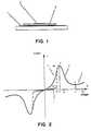
- Figure lis a cross-sectional view of a representative device of this invention wherein electrodes (l) and (2) are separated by the thin film (3).
- this Figureexemplifies a sandwich electrode configuration, such an arrangement is not critical and nearly any configuration appropriate for a given device application may be used. For example, arrangements such as coplanar, transplanar, crossed grid arrays, two dimensional circular dot pattern, etc. may be used.
- the shape of the electrodes and the materials from which they are constructedmay be any conventionally known in the art.
- the electrodescan be made of nearly any electrically conductive or semiconductive material such as gold, silver, aluminum, platinum, copper, gallium arsenide, chromium, silicon, etc.
- the electrodescan be used in nearly any shape or form desired, such as a wire or a conventional lead, provided they have at least enough device area to enable the desired current flow. Particularly preferred herein is the use of gold electrodes.
- the electrodesmay be formed on the thin film by evaporating or sputtering the appropriate electrode material in vacuum.
- the thin filmmay be deposited directly onto preformed electrodes to create the appropriate contact or the preformed electrodes may be adhered to the thin film by conventional techniques.
- the thin films (3) of this inventioncomprise silicon dioxide derived from hydrogen silsesquioxane resin. Generally, these films may be of any thickness desired. Those in the range of between about 50 and 5,000 nanometers are, however, preferred with those in the range of between about l00 and 600 nanometers being especially preferred.
- Such thin filmsmay be formed by any appropriate method.
- a particularly preferred techniquecomprises coating a substrate with a solution comprising a solvent and hydrogen silsesquioxane resin, evaporating the solvent to form a preceramic coating and then converting the preceramic coating to the thin film.
- Other equivalent methodsare also contemplated herein.
- the hydrogen silsesquioxane resins which may be used in this inventionare those with the structure (HSiO 3/2 ) n .
- Such resinsare generally produced by the hydrolysis and condensation of silanes of the formula HSiX3, wherein X is a hydrolyzable group and they may be either fully hydrolyzed and condensed (HSiO 3/2 ) n or their hydrolysis or condensation may be interrupted at an intermediate point such that partial hydrolyzates (which contain Si-OR groups wherein OR is a hydrolyzable group) and/or partial condensates (which contain SiOH groups) are formed.
- these resinsmay contain a small percentage of silicon atoms which have either no hydrogen atoms or more than one hydrogen atom attached thereto due to various factors involved in their formation or handling.
- H-resinwhich may contain up to l00-300 ppm silanol
- the resultant polymeric materialhas units of the formula (HSiO 3/2 ) n in which n is generally 8-l000 and has a number average molecular weight of from about 800-2900 and a weight average molecular weight of between about 8000-28,000.
- the H-resinis then deposited on the surface of the substrate.
- Thiscan be accomplished in any manner, but a preferred method involves dissolving the H-resin in a solvent to form a solution and then applying this solution to the surface of the substrate.
- Various facilitating measuressuch as stirring and/or heating may be used to aid in the dissolution.
- Solvents which may be usedinclude any agent or mixture of agents which will dissolve the H-resin to form a homogenous solution without affecting the thin film or its switching properties.
- solventscan include, for example, alcohols such as ethyl or isopropyl, aromatic hydrocarbons such as benzene or toluene, alkanes such as n-heptane or dodecane, ketones, esters, glycol ethers or cyclic dimethylpolysiloxanes, in an amount sufficient to dissolve the above materials to low solids. Generally, enough of the above solvent is used to form a 0.l-50 weight percent solution.
- the coating solutionmay also include a modifying ceramic oxide precursor such that the resultant ceramic coating comprises a mixed silicon/metal oxide.
- a modifying ceramic oxide precursorsuch that the resultant ceramic coating comprises a mixed silicon/metal oxide.
- Such precursorscan include, for example, compounds of various metals, such as iron, aluminum, titanium, zirconium, tantalum, niobium and/or vanadium. These compounds generally form either solutions or dispersion when mixed with the H-resin and must be capable of being subsequently pyrolyzed at relatively low temperatures and relatively rapid reaction rates to form modifying ceramic oxide coatings.
- a modifying ceramic oxide precursorit is generally present in the preceramic mixture in an amount such that the final coating contains 0.l to 30 percent by weight modifying ceramic oxide.
- modifying ceramic oxide precursorsinclude tetra n-propoxy zirconium, tetraisobutoxy titanium, aluminum trispentanedionate, pentaethoxy tantalum, tripropoxy vanadium, pentaethoxy niobium, zirconium pentanedionate and titanium dibutoxy bispentanedionate.
- modifying ceramic oxide precursorsare to be included in the H-resin preceramic solution, they may be simply dissolved in the solution comprising the H-resin and the solvent and allowed to stand at room temperature for a time sufficient to allow the modifying ceramic oxide precursor to react into the structure of the H-resin. Generally, a period of greater than about 2 hours is necessary for said reaction to occur.
- the solutionmay then be applied to the substrate as discussed infra .
- the modifying ceramic oxide precursormay be hydrolyzed or partially hydrolyzed, dissolved in the solution comprising the solvent and H-resin and then immediately applied to the substrate.
- Various facilitating measuressuch as stirring or agitation may be used as necessary to produce said solutions.
- a platinum, rhodium or copper catalystmay also be used herein to increase the rate and extent of hydrogen silsesquioxane resin conversion to silicon dioxide.
- any platinum, rhodium or copper compound or complex which can be solubilizedwill be functional.
- an compositionsuch as platinum acetylacetonate, rhodium catalyst RhCl3[S(CH2CH2CH2CH3)2]3, obtained from Dow Corning Corporation, Midland, Mich. or cupric naphthenate are all within the scope of this invention.
- These catalystsare generally added in an amount of between about 5 to l000 ppm platinum, rhodium or copper based on the weight of H-resin.
- the coating solutionis applied by techniques such as spin coating, dip coating, spray coating or flow coating and the solvent allowed to evaporate. Any suitable means of evaporation may be used such as simple air drying by exposure to an ambient environment or by the application of a vacuum or mild heat.
- the resultant preceramic coatingis then converted to the silicon dioxide thin film. Generally, this is done at a temperature and in an environment which will not result in the formation of a fully dense film (2.2 g/cc). For instance, such silicon dioxide films may be formed by heating the preceramic coating in air at a temperature of from about l00 to about 600°C. For other environments (eg. ammonia, oxygen, nitrogen, etc.), however, the temperature may vary.
- the resultant thin filmis not completely dense so that the observed behavior can occur.
- the exact densityis not critical and can vary over a wide range. Generally, the density is in the range of between about 40 and 95%, with densities in the range of between about 60 and 90% being preferred.
- the necessary electrodesare attached in the manner described above such that a voltage can be applied across the thin film.
- a newly created device prepared in this mannerinitially exhibits an undefined, non-specific resistance. For instance, some devices may exhibit resistance values as low as l ohm while others exhibit values above l0 megohm. Those with very low resistance often have shorts between the electrodes due to pin holes and other device flaws. If present, such shorts should be "blown out” by applying a voltage sufficiently high to vaporize the electrode around the short (eg., l0-20 V from a low impedance voltage source).
- the devices of the inventionmay be placed in a non-oxidizing environment.
- suitable environmentsinclude nitrogen, argon, helium, carbon dioxide and the like.
- establishing a vacuum or encapsulating the devicecan also provide the desired environment.
- the following discussiondescribes the characteristics of a typical device formed in the above manner and the procedures to switch the device from its ON state to an OFF state and back again.
- the typical deviceconsists of a silica thin film with a thickness of about 200 nanometers and device area of about 0.l cm2.
- a voltage(measured in volt (V)) is applied across the electrodes and the current through the device as well as the voltage across the device are both measured.
- the current, measured in ampere (A)is converted to a current density and given in ampere/cm2.
- the resultsare plotted in a diagram of current vs. voltage and referred to as a jV curve.
- the following valuesare only representative of the above device and are not meant to be limiting.
- Threshold switchingis similar to that known in the art for other thin films.
- the thin filmexhibits a high impedance as would normally be associated with an insulator.
- the resistivity of the device in this "OFF" stateis generally in the range of between about l08 ohm cm and about l0 ll ohm cm.
- the resistivity in this "ON" stateis typically in the range of between about l04 ohm cm and about l07 ohm cm.
- the jV tracingfollows lines 2, 3 and 4 wherein the current rises steeply with voltage in the first quadrant (line 2)(and, symmetrically to it, in the third quadrant) until it reaches a maximum current, (p), at a voltage (y). Increasing the voltage beyond this value results in a decrease in current density until a minimum (q) is reached at voltage (z), i.e., the device exhibits a voltage controlled negative differential resistance or NDR (line 3).
- the values for (y)range between 4-6 V and for (z) between 8-l0 V. At voltages above (z), the jV curve show the high resistivity characteristic of an insulator (line 4).
- jV curveis wide and "stable" in the NDR region, i.e., no uncontrollable transitions occur as the applied voltage is changed, although the jV curve is noisier in this region than in the low voltage part (line 2).
- any point on the jV curvecan be isolated and maintained, provided the source impedance of the voltage supply is smaller by magnitude than the negative differential resistance of the device at that point.
- the jV curve of the device in its ON statecan be completely traced out for both increasing and decreasing voltages, through the maximum, at a sufficiently low rate of change of the applied voltage.
- the curveis continuous through the origin which means (i) there is no holding current necessary to maintain the ON state and (ii) the device has a "memory" of the ON state even when no voltage is applied.
- a device in the ON statemay be turned OFF by a voltage pulse starting from zero, provided the pulse voltage is larger or approximately equal to (z) (i.e., the pulse reaches into line 4) and the fall time of the pulse meets the slew rate requirement.
- a voltage of l0 V for a duration of l microsecond or longeris adequate.
- the deviceWhen the device is turned OFF in the above manner, it has a high resistance, typically 2 or 3 orders of magnitude higher than in the ON state.
- the resistancecan be determined by measuring the jV curve in the OFF state over a small range of the applied voltage (up to the threshold voltage). The device will remain in the OFF state as long as the applied voltage does not exceed the threshold voltage. Such a device in the OFF state can be converted to the ON state as described above.
- the mechanism for the effects described aboveis not fully known, the inventors have shown that the nanostructure of the thin film is essential for switching and negative differential resistance.
- the structure of the electronic states associated with the internal surfaces of silicon dioxide derived form hydrogen silsesquioxaneare assumed to be responsible for the behavior of the material.
- the mechanism for switching between the ON and OFF statesis proposed to be a solid-state electrochemical redox reaction between the electronic states discussed above.
- Figure 4shows the device created by this example.
- 8 contact pads (3)were applied to a 2.54 x 3.8l cm (l ⁇ x l.5 ⁇ ) Corning 7059 glass slide (l) by a silk screening process using gold frit paste (conductive coating #8835 by Electroscience Laboratories). The slide with the silk screened contact pads was dried in air at l50°C. and then baked at 520°C. for 30 minutes. Back electrodes (4) were then deposited across the contact pads.
- Electrodeswere deposited by a process which comprised placing the slide in a deposition chamber which was pumped down to l mPa using liquid nitrogen in a cold trap, establishing an argon glow discharge therein at a suitable pressure between l.5 and 3 kilovolts for l0 minutes and evaporating a 3 nm thick layer of chromium and a l80 nm thick layer of gold through a stainless steel mask.
- the contact pads on the slidewere masked and a l35 nm thick silicon dioxide thin film (2) was then applied to the surface of the slide.
- the thin filmwas applied by diluting hydrogen silsesquioxane resin (prepared by the method of Bank et al. in U.S. Patent No. 5,0l0,l59) to about l0% in a cyclic dimethylpolysiloxane solvent, coating the surface of the slide with this solution, spinning the slide at 3000 RPM for l0 seconds and pyrolyzing the slide in a furnace in air for 3 hours at 400°C. to form the thin film.
- hydrogen silsesquioxane resinprepared by the method of Bank et al. in U.S. Patent No. 5,0l0,l59
- Top electrodes (5)were then deposited on the thin film by the same process as before which comprised placing the slide in a deposition chamber which was pumped down to l mPa using liquid nitrogen in a cold trap and then evaporating a l00 nm thick layer of gold through a stainless steel mask.
- the area of the devicewas 0.l5 cm2.
- This devicewas then mounted in a measurement chamber where the electrodes of one of the four devices were connected to the measuring equipment by applying wires to the contact pads. The chamber was then purged with nitrogen and a variable voltage was applied across the thin film. The voltage V across the device and the current I through the device were measured for each voltage and the current density j was calculated from the device area A.
- a devicewas created in the same manner as in Example l except for the method of film formation.
- the thin filmwas applied by diluting hydrogen silsesquioxane resin (prepared by the method of Bank et al. in U.S. Patent No. 5,0l0,l59) to about 25% solids in a solvent comprising a mixture of heptane (5% by wt) and dodecane (95% by wt), coating the surface of the slide with this solution, spinning the slide at 3000 RPM for l0 seconds and pyrolyzing the slide in a furnace in air for 3 hours at 400°C.
- the resultant filmwas about 450 nm thick.
- a second thin filmwas deposited on top of the first in the same manner as before.
- the dual layer filmwas then approximately 9l0 nm thick.
- a devicewas created in the same manner as in Example l except for the method of film formation.
- a coating solutionwas formed by mixing 0.462 g Fe(O2C5H7)3, 0.487 g hydrogen silsesquioxane resin (prepared by the method of Bank et al. in U.S. Patent No. 5,0l0,l59) and 9.9 g 2,4 pentandione. This solution was coated onto the surface of the slide, the slide was spun at l500 RPM for l5 seconds and the coated slide was pyrolyzed in a furnace in air for l hours at 400°C.
- a devicewas created in the same manner as in Example l except for the method of film formation.
- the thin filmwas formed from Accuglas TM 305 (lot 7794) (an organopolysiloxane) by coating the surface of the slide with this solution, spinning the slide at 3000 RPM for l0 seconds and pyrolyzing the slide in a furnace in air for l hour at 400°C.
- the resultant filmwas about 200 nm thick.
- Top electrodeswere then deposited in the same manner as Example l.
- the j-V characteristicswere measured and are displayed in Figure 6.
- This Figureshows that thin films derived from other silica precursors differ from those derived from H-resin. Specifically, this Figure shows that the threshold voltage for the ON transition is much lower, the NDR regime is wide and noisy and the jV characteristic is erratic.
- a devicewas created in the same manner as in Example l except for the method of film formation.
- the thin filmwas formed by a vapor deposition process which comprised placing the slide in an electron cyclotron resonance reactor and kept at a substrate temperature of 450°C.
- the resultant filmwas about l70 nm thick.
- Top electrodeswere then deposited in the same manner as Example l.
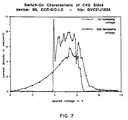
- the j-V characteristicswere measured and are displayed in Figure 7.
- This Figureshows that thin films formed by chemical vapor deposition differ from those derived from H-resin. Specifically, this Figure shows l) a low ON current and small ON/OFF ratio, 2) higher threshold voltage for ON transition, 3) a very steep NDR regime and 4) the jV characteristic is erratic.
Landscapes
- Engineering & Computer Science (AREA)
- Physics & Mathematics (AREA)
- Theoretical Computer Science (AREA)
- Health & Medical Sciences (AREA)
- Life Sciences & Earth Sciences (AREA)
- Biomedical Technology (AREA)
- Biophysics (AREA)
- Neurology (AREA)
- Mathematical Physics (AREA)
- Data Mining & Analysis (AREA)
- Evolutionary Computation (AREA)
- General Health & Medical Sciences (AREA)
- Molecular Biology (AREA)
- Computing Systems (AREA)
- General Engineering & Computer Science (AREA)
- General Physics & Mathematics (AREA)
- Computational Linguistics (AREA)
- Software Systems (AREA)
- Artificial Intelligence (AREA)
- Manufacturing & Machinery (AREA)
- Formation Of Insulating Films (AREA)
- Semiconductor Memories (AREA)
- Liquid Deposition Of Substances Of Which Semiconductor Devices Are Composed (AREA)
- Application Of Or Painting With Fluid Materials (AREA)
- Silicon Compounds (AREA)
Abstract
Description
- This invention relates to a method of forming threshold switching devices which exhibit negative differential resistance and to the devices formed thereby. The method comprises depositing a silicon dioxide film derived from hydrogen silsesquioxane resin between at least two electrodes and applying a voltage above a threshold voltage across the electrodes.
- Numerous devices which exhibit threshold switching are known in the art. For example, Ovshinsky in U.S. Patent No. 3,27l,59l describes such devices in which semiconductor materials, such as crystalline or amorphous tellurides, selenides, sulfides or oxides of substantially any metal, are deposited between electrodes. The semiconductors and methods specifically set forth in this reference, however, are not the same as those claimed herein. As such, the j-V curves in this reference differ from those of the present application.
- Threshold switching with negative differential resistance is also known in various metal oxide thin films. For instance, Bullot et al., Phys. Stat. Sol. (a) 7l, Kl (l982), describe threshold switching in vanadium oxide layers deposited from gels; Ansari et al., J. Phys. D:Appl. Phys. 20 (l987) l063-l066 describe threshold switching in titanium oxide films formed by thermally oxidizing a titanium metal layer; Ramesham et al., NASA Tech Briefs, December l989, p. 28, describe the switching in manganese oxide films; and Morgan et al., Thin Solid Films, l5 (l973) l23-l3l, describe switching and negative differential resistance in aluminum oxide films. The materials and characteristics described in these references, however, differ from those described herein.
- The switching and negative differential resistance characteristics of silicon oxide films have likewise been described. For instance, Simmons, Handbook of Thin Film Technology, Chapter l4 (l970), describes electronic conduction through thin insulating films, including silicon oxide, as well as their negative resistance and memory characteristics; Al-Ismail et al., J. Mat. Sci. 20 (l985) 2l86-2l92, describe switching and negative resistance in a copper-silicon oxide-copper system; Morgan et al., Thin Solid Films, 20 (l974) S7-S9, describe threshold switching and memory in silicon oxide films; Boelle et al., Applied Surface Science 46 (l990) 200-205, describe the current-voltage characteristics of silica films derived from sol-gel low temperature methods; and Klein, J. Appl. Phys., 40 (l969) 2728-2740, describes the electrical breakdown of silicon oxide films. As with the prior metal oxide references, however, these too do not describe the methods and characteristics described herein.
- Thin film silica coatings derived from hydrogen silsesquioxane resin are also known in the art. For instance, Haluska et al. in U.S. Patent No. 4,756,977 describe forming such films by diluting hydrogen silsesquioxane resin in a solvent, applying the solution to a substrate, drying the solvent and heating. Such coatings are taught therein to provide protection and electrical insulation.
- The present inventors have now found that switching devices with desirable features can be formed by depositing a thin, hydrogen silsesquioxane derived silicon dioxide film between at least 2 electrodes and applying a voltage above a threshold voltage across the electrodes.
- The present invention relates to a method of forming a threshold switching device having negative differential resistance. The method comprises depositing a non-dense silicon dioxide film derived from hydrogen silsesquioxane resin between at least two electrodes. A voltage above a certain threshold voltage is then applied across the electrodes to complete formation of the device.
- The device formed in this manner is characterized in that l) the conductive state of the thin film can be converted to the resistive state with memory by decreasing the applied voltage from a sufficiently high value to a value below the threshold voltage at a sufficiently high rate, 2) it can be converted from a resistive state to a conductive state with memory by the application of a threshold voltage and 3) the application of voltage above a threshold voltage results in the film exhibiting stable negative differential resistance.
- The present invention is based on the discovery that thin films of silicon dioxide derived from hydrogen silsesquioxane resin (thin films) exhibit novel threshold switching and negative differential resistance. This was particularly unexpected since the thin films herein are conventionally used as electrical insulation materials.
- These novel devices show features beyond those taught in the prior art. For instance:
- 1. The devices can carry high current density (eg., l Amp/cm²);
- 2. The devices have been shown to operate with thick films (eg., l micrometers) whereas the prior art teaches that the effect does mot occur in films greater than 0.5 micrometers thick; and
- 3. The whole jV curve, especially the negative differential resistance region, has been shown to be stable and monotonic.
- As used in this disclosure, the expressions "hydrogen silsesquioxane resin" or "H-resin" are meant to include those hydridosilane resins which are fully condensed [(HSiO3/2)n] as well as those which are only partially hydrolyzed and/or partially condensed and, thereby, may contain residual SiOR and/or SiOH substituents (wherein OR is a hydrolyzable group); and the expression "thin film" is used to describe the silicon dioxide films derived from hydrogen silsesquioxane.
- The invention will be described with specific reference to the figures. Figure l is a cross-sectional view of a representative device of this invention wherein electrodes (l) and (2) are separated by the thin film (3). Although this Figure exemplifies a sandwich electrode configuration, such an arrangement is not critical and nearly any configuration appropriate for a given device application may be used. For example, arrangements such as coplanar, transplanar, crossed grid arrays, two dimensional circular dot pattern, etc. may be used.
- The shape of the electrodes and the materials from which they are constructed may be any conventionally known in the art. For instance, the electrodes can be made of nearly any electrically conductive or semiconductive material such as gold, silver, aluminum, platinum, copper, gallium arsenide, chromium, silicon, etc. Likewise, the electrodes can be used in nearly any shape or form desired, such as a wire or a conventional lead, provided they have at least enough device area to enable the desired current flow. Particularly preferred herein is the use of gold electrodes.
- Contact between the electrodes and the thin film can be established by techniques well known in the art. For instance, the electrodes may be formed on the thin film by evaporating or sputtering the appropriate electrode material in vacuum. Alternatively, the thin film may be deposited directly onto preformed electrodes to create the appropriate contact or the preformed electrodes may be adhered to the thin film by conventional techniques.
- The thin films (3) of this invention comprise silicon dioxide derived from hydrogen silsesquioxane resin. Generally, these films may be of any thickness desired. Those in the range of between about 50 and 5,000 nanometers are, however, preferred with those in the range of between about l00 and 600 nanometers being especially preferred.
- Such thin films may be formed by any appropriate method. A particularly preferred technique comprises coating a substrate with a solution comprising a solvent and hydrogen silsesquioxane resin, evaporating the solvent to form a preceramic coating and then converting the preceramic coating to the thin film. Other equivalent methods, however, are also contemplated herein.
- As defined above, the hydrogen silsesquioxane resins which may be used in this invention are those with the structure (HSiO3/2)n. Such resins are generally produced by the hydrolysis and condensation of silanes of the formula HSiX₃, wherein X is a hydrolyzable group and they may be either fully hydrolyzed and condensed (HSiO3/2)n or their hydrolysis or condensation may be interrupted at an intermediate point such that partial hydrolyzates (which contain Si-OR groups wherein OR is a hydrolyzable group) and/or partial condensates (which contain SiOH groups) are formed. Though not represented by this structure, these resins may contain a small percentage of silicon atoms which have either no hydrogen atoms or more than one hydrogen atom attached thereto due to various factors involved in their formation or handling.
- Various methods for the production of these resins have been developed. For instance, Collins et al. in U.S. Patent No. 3,6l5,272, describe a process of forming nearly fully condensed H-resin (which may contain up to l00-300 ppm silanol) comprising hydrolyzing trichlorosilane in a benzenesulfonic acid hydrate hydrolysis medium and then washing the resultant resin with water or aqueous sulfuric acid. The resultant polymeric material has units of the formula (HSiO3/2)n in which n is generally 8-l000 and has a number average molecular weight of from about 800-2900 and a weight average molecular weight of between about 8000-28,000.
- Similarly, Bank et al. in U.S. Patent No. 5,0l0,l59 teach methods of forming such resins (which may contain up to l000 ppm silanol) comprising hydrolyzing hydridosilanes in an arylsulfonic acid hydrate hydrolysis medium to form a resin which is then contacted with a neutralizing agent. A preferred embodiment of this latter process uses an acid to silane ratio of about 6/l.
- Other methods, such as those described by Frye et al. in U.S. Patent No. 4,999,397, comprising hydrolyzing trichlorosilane in a non-sulfur containing polar organic solvent by the addition of water or HCl and a metal oxide or a method which comprises hydrolyzing a hydrocarbonoxy hydridosilane with water in an acidified oxygen-containing polar organic solvent, also produce such hydridosiloxane resins and are functional herein.
- The H-resin is then deposited on the surface of the substrate. This can be accomplished in any manner, but a preferred method involves dissolving the H-resin in a solvent to form a solution and then applying this solution to the surface of the substrate. Various facilitating measures such as stirring and/or heating may be used to aid in the dissolution. Solvents which may be used include any agent or mixture of agents which will dissolve the H-resin to form a homogenous solution without affecting the thin film or its switching properties. These solvents can include, for example, alcohols such as ethyl or isopropyl, aromatic hydrocarbons such as benzene or toluene, alkanes such as n-heptane or dodecane, ketones, esters, glycol ethers or cyclic dimethylpolysiloxanes, in an amount sufficient to dissolve the above materials to low solids. Generally, enough of the above solvent is used to form a 0.l-50 weight percent solution.
- Besides H-resin, the coating solution may also include a modifying ceramic oxide precursor such that the resultant ceramic coating comprises a mixed silicon/metal oxide. Such precursors can include, for example, compounds of various metals, such as iron, aluminum, titanium, zirconium, tantalum, niobium and/or vanadium. These compounds generally form either solutions or dispersion when mixed with the H-resin and must be capable of being subsequently pyrolyzed at relatively low temperatures and relatively rapid reaction rates to form modifying ceramic oxide coatings. When such a modifying ceramic oxide precursor is used, it is generally present in the preceramic mixture in an amount such that the final coating contains 0.l to 30 percent by weight modifying ceramic oxide.
- Examples of modifying ceramic oxide precursors include tetra n-propoxy zirconium, tetraisobutoxy titanium, aluminum trispentanedionate, pentaethoxy tantalum, tripropoxy vanadium, pentaethoxy niobium, zirconium pentanedionate and titanium dibutoxy bispentanedionate.
- If modifying ceramic oxide precursors are to be included in the H-resin preceramic solution, they may be simply dissolved in the solution comprising the H-resin and the solvent and allowed to stand at room temperature for a time sufficient to allow the modifying ceramic oxide precursor to react into the structure of the H-resin. Generally, a period of greater than about 2 hours is necessary for said reaction to occur. The solution may then be applied to the substrate as discussedinfra. Alternatively, the modifying ceramic oxide precursor may be hydrolyzed or partially hydrolyzed, dissolved in the solution comprising the solvent and H-resin and then immediately applied to the substrate. Various facilitating measures such as stirring or agitation may be used as necessary to produce said solutions.
- A platinum, rhodium or copper catalyst may also be used herein to increase the rate and extent of hydrogen silsesquioxane resin conversion to silicon dioxide. Generally, any platinum, rhodium or copper compound or complex which can be solubilized will be functional. For instance, an composition such as platinum acetylacetonate, rhodium catalyst RhCl₃[S(CH₂CH₂CH₂CH₃)₂]₃, obtained from Dow Corning Corporation, Midland, Mich. or cupric naphthenate are all within the scope of this invention. These catalysts are generally added in an amount of between about 5 to l000 ppm platinum, rhodium or copper based on the weight of H-resin.
- If the above solution method is used, the coating solution is applied by techniques such as spin coating, dip coating, spray coating or flow coating and the solvent allowed to evaporate. Any suitable means of evaporation may be used such as simple air drying by exposure to an ambient environment or by the application of a vacuum or mild heat.
- The resultant preceramic coating is then converted to the silicon dioxide thin film. Generally, this is done at a temperature and in an environment which will not result in the formation of a fully dense film (2.2 g/cc). For instance, such silicon dioxide films may be formed by heating the preceramic coating in air at a temperature of from about l00 to about 600°C. For other environments (eg. ammonia, oxygen, nitrogen, etc.), however, the temperature may vary.
- It is generally important that the resultant thin film is not completely dense so that the observed behavior can occur. The exact density, however, is not critical and can vary over a wide range. Generally, the density is in the range of between about 40 and 95%, with densities in the range of between about 60 and 90% being preferred.
- After the thin film is formed, the necessary electrodes are attached in the manner described above such that a voltage can be applied across the thin film.
- A newly created device prepared in this manner initially exhibits an undefined, non-specific resistance. For instance, some devices may exhibit resistance values as low as l ohm while others exhibit values above l0 megohm. Those with very low resistance often have shorts between the electrodes due to pin holes and other device flaws. If present, such shorts should be "blown out" by applying a voltage sufficiently high to vaporize the electrode around the short (eg., l0-20 V from a low impedance voltage source).
- Voltage is then slowly applied .across the film of the device and increased until the threshold voltage is reached, at which point the resistance of the device suddenly falls. Upon such a voltage application, the device is completely formed and it remains in its low resistance state.
- To obtain lower threslold voltages and more reproducible results, the devices of the invention may be placed in a non-oxidizing environment. Examples of suitable environments include nitrogen, argon, helium, carbon dioxide and the like. Alternatively, however, establishing a vacuum or encapsulating the device can also provide the desired environment.
- The following discussion describes the characteristics of a typical device formed in the above manner and the procedures to switch the device from its ON state to an OFF state and back again. The typical device consists of a silica thin film with a thickness of about 200 nanometers and device area of about 0.l cm². A voltage (measured in volt (V)) is applied across the electrodes and the current through the device as well as the voltage across the device are both measured. The current, measured in ampere (A) is converted to a current density and given in ampere/cm². The results are plotted in a diagram of current vs. voltage and referred to as a jV curve. The following values are only representative of the above device and are not meant to be limiting.
- Threshold switching, as displayed by this device, is similar to that known in the art for other thin films. As voltage less than the threshold voltage (about 3 volts) is applied to an electrode thereon, the thin film exhibits a high impedance as would normally be associated with an insulator. The resistivity of the device in this "OFF" state is generally in the range of between about l0⁸ ohm cm and about l0ll ohm cm. When the applied voltage is raised above this threshold voltage, however, the thin film is rapidly converted to a state of low resistivity and the device supports a high current density. The resistivity in this "ON" state is typically in the range of between about l0⁴ ohm cm and about l0⁷ ohm cm.
- This threshold switching behavior is graphically displayed in Figure 2. Line l shows that when the device is in the OFF state, the current density increases only slightly as the applied voltage is increased. When the applied voltage reaches the threshold voltage, x, the device rapidly switches from the OFF state to the ON state wherein the current density is suddenly increased by 2 or three orders of magnitude or more (dotted line).
- Once in this ON state, the jV tracing follows
lines - Especially advantageous in devices of this invention is the fact that the jV curve is wide and "stable" in the NDR region, i.e., no uncontrollable transitions occur as the applied voltage is changed, although the jV curve is noisier in this region than in the low voltage part (line 2). Thus, any point on the jV curve can be isolated and maintained, provided the source impedance of the voltage supply is smaller by magnitude than the negative differential resistance of the device at that point.
- The jV curve of the device in its ON state can be completely traced out for both increasing and decreasing voltages, through the maximum, at a sufficiently low rate of change of the applied voltage. In particular, the curve is continuous through the origin which means (i) there is no holding current necessary to maintain the ON state and (ii) the device has a "memory" of the ON state even when no voltage is applied.
- To convert the device from the ON state to the OFF state requires that the applied voltage be removed or reduced to a value around zero at a sufficiently high slew rate from a voltage above (z). As shown in Figure 3, the jV curve of the device does not go through the current peak (p) when the applied voltage is rapidly lowered in this manner. Rather, it follows a direct, nearly linear path (line 5). Typical slew rates for efficiently switching the device OFF are greater than about l V/millisecond with rates greater than about l V/microsecond being preferred. It is to be noted that a device in the ON state may be turned OFF by a voltage pulse starting from zero, provided the pulse voltage is larger or approximately equal to (z) (i.e., the pulse reaches into line 4) and the fall time of the pulse meets the slew rate requirement. Typically, a voltage of l0 V for a duration of l microsecond or longer is adequate.
- When the device is turned OFF in the above manner, it has a high resistance, typically 2 or 3 orders of magnitude higher than in the ON state. The resistance can be determined by measuring the jV curve in the OFF state over a small range of the applied voltage (up to the threshold voltage). The device will remain in the OFF state as long as the applied voltage does not exceed the threshold voltage. Such a device in the OFF state can be converted to the ON state as described above.
- Although the mechanism for the effects described above is not fully known, the inventors have shown that the nanostructure of the thin film is essential for switching and negative differential resistance. In particular, the structure of the electronic states associated with the internal surfaces of silicon dioxide derived form hydrogen silsesquioxane are assumed to be responsible for the behavior of the material. The mechanism for switching between the ON and OFF states is proposed to be a solid-state electrochemical redox reaction between the electronic states discussed above.
- The effects described above suggest potential applications for these devices as switches, sensors, memory elements, etc.
- The following non-limiting examples are provided so that those skilled in the art will understand the invention.
- Figure 4 shows the device created by this example. 8 contact pads (3) were applied to a 2.54 x 3.8l cm (l˝ x l.5˝) Corning 7059 glass slide (l) by a silk screening process using gold frit paste (conductive coating #8835 by Electroscience Laboratories). The slide with the silk screened contact pads was dried in air at l50°C. and then baked at 520°C. for 30 minutes. Back electrodes (4) were then deposited across the contact pads. These electrodes were deposited by a process which comprised placing the slide in a deposition chamber which was pumped down to l mPa using liquid nitrogen in a cold trap, establishing an argon glow discharge therein at a suitable pressure between l.5 and 3 kilovolts for l0 minutes and evaporating a 3 nm thick layer of chromium and a l80 nm thick layer of gold through a stainless steel mask.
- The contact pads on the slide were masked and a l35 nm thick silicon dioxide thin film (2) was then applied to the surface of the slide. The thin film was applied by diluting hydrogen silsesquioxane resin (prepared by the method of Bank et al. in U.S. Patent No. 5,0l0,l59) to about l0% in a cyclic dimethylpolysiloxane solvent, coating the surface of the slide with this solution, spinning the slide at 3000 RPM for l0 seconds and pyrolyzing the slide in a furnace in air for 3 hours at 400°C. to form the thin film.
- Top electrodes (5) were then deposited on the thin film by the same process as before which comprised placing the slide in a deposition chamber which was pumped down to l mPa using liquid nitrogen in a cold trap and then evaporating a l00 nm thick layer of gold through a stainless steel mask. The area of the device was 0.l5 cm².
- This device was then mounted in a measurement chamber where the electrodes of one of the four devices were connected to the measuring equipment by applying wires to the contact pads. The chamber was then purged with nitrogen and a variable voltage was applied across the thin film. The voltage V across the device and the current I through the device were measured for each voltage and the current density j was calculated from the device area A.
- The j-V curve of Figure 5 was obtained from this device. This curve clearly shows the transition of the device from its OFF state to its ON state as well as a full curve of the device in its ON state.
- A device was created in the same manner as in Example l except for the method of film formation. In this example, the thin film was applied by diluting hydrogen silsesquioxane resin (prepared by the method of Bank et al. in U.S. Patent No. 5,0l0,l59) to about 25% solids in a solvent comprising a mixture of heptane (5% by wt) and dodecane (95% by wt), coating the surface of the slide with this solution, spinning the slide at 3000 RPM for l0 seconds and pyrolyzing the slide in a furnace in air for 3 hours at 400°C. The resultant film was about 450 nm thick. After this film had cooled, a second thin film was deposited on top of the first in the same manner as before. The dual layer film was then approximately 9l0 nm thick.
- Top electrodes were then deposited in the same manner as Example l. The j-V characteristics were measured and showed nearly the same results as Example l.
- This example shows that the thin films of this invention are not thickness limited as in the prior art.
- A device was created in the same manner as in Example l except for the method of film formation. In this example a coating solution was formed by mixing 0.462 g Fe(O₂C₅H₇)₃, 0.487 g hydrogen silsesquioxane resin (prepared by the method of Bank et al. in U.S. Patent No. 5,0l0,l59) and 9.9
g - Top electrodes were then deposited in the same manner as Example l. The j-V characteristics were measured and showed nearly the same results as Example l.
- A device was created in the same manner as in Example l except for the method of film formation. In this example, the thin film was formed from AccuglasTM 305 (lot 7794) (an organopolysiloxane) by coating the surface of the slide with this solution, spinning the slide at 3000 RPM for l0 seconds and pyrolyzing the slide in a furnace in air for l hour at 400°C. The resultant film was about 200 nm thick.
- Top electrodes were then deposited in the same manner as Example l. The j-V characteristics were measured and are displayed in Figure 6. This Figure shows that thin films derived from other silica precursors differ from those derived from H-resin. Specifically, this Figure shows that the threshold voltage for the ON transition is much lower, the NDR regime is wide and noisy and the jV characteristic is erratic.
- A device was created in the same manner as in Example l except for the method of film formation. In this example, the thin film was formed by a vapor deposition process which comprised placing the slide in an electron cyclotron resonance reactor and kept at a substrate temperature of 450°C. A source gas mixture of 25% SiH₄ and 75% Ar and O₂ for a ratio of O₂:SiH₄ = 2.2:l was admitted into the reactor at a total pressure of l Pa and a microwave plasma was maintained in the reactor at a power of 400 W for l2 minutes. The resultant film was about l70 nm thick.
- Top electrodes were then deposited in the same manner as Example l. The j-V characteristics were measured and are displayed in Figure 7. This Figure shows that thin films formed by chemical vapor deposition differ from those derived from H-resin. Specifically, this Figure shows l) a low ON current and small ON/OFF ratio, 2) higher threshold voltage for ON transition, 3) a very steep NDR regime and 4) the jV characteristic is erratic.
Claims (9)
- A method of forming a threshold switching device having negative differential resistance comprising creating a device by depositing a non-dense silicon dioxide film derived from hydrogen silsesquioxane resin between at least two electrodes and applying a voltage above the threshold voltage across the electrodes.
- The method of claim 1 wherein the silicon dioxide film is deposited by a process which comprises coating a substrate with a solution comprising a solvent and hydrogen silsesquioxane resin, evaporating the solvent to form a preceramic coating and then pyrolyzing the preceramic coating.
- The method of claim 1 wherein the device is placed in non-oxidizing atmosphere.
- A method of forming a threshold switching device having negative differential resistance comprising creating a device by depositing a no-dense film comprising silicon dioxide and one or more modifying ceramic oxides between at least two electrodes and applying a voltage above the threshold voltage across the electrodes, wherein the silicon oxide and a modifying ceramic oxide film is derived from hydrogen silsesquioxane resin and a modifying ceramic oxide precursor.
- The method of claim 4 wherein the film is deposited by a process which comprises coating a substrate with a solution comprising a solvent, hydrogen silsesquioxane resin and the modifying ceramic oxide precursor, evaporating the solvent to form a preceramic coating and then pyrolyzing the preceramic coating.
- The method of claim 4 wherein the device is placed in non-oxidizing atmosphere.
- A threshold switching device comprising at least 2 leads in direct contact with a material comprising silica derived from hydrogen silsesquioxane.
- The device of claim 7 wherein the device is in non- oxidizing atmosphere.
- The device of claim 7 wherein the material also comprises one or more modifying ceramic oxide.
Applications Claiming Priority (2)
| Application Number | Priority Date | Filing Date | Title |
|---|---|---|---|
| US694721 | 1991-05-02 | ||
| US07/694,721US5312684A (en) | 1991-05-02 | 1991-05-02 | Threshold switching device |
Publications (3)
| Publication Number | Publication Date |
|---|---|
| EP0512717A2true EP0512717A2 (en) | 1992-11-11 |
| EP0512717A3 EP0512717A3 (en) | 1993-06-30 |
| EP0512717B1 EP0512717B1 (en) | 1995-06-07 |
Family
ID=24790016
Family Applications (1)
| Application Number | Title | Priority Date | Filing Date |
|---|---|---|---|
| EP19920303695Expired - LifetimeEP0512717B1 (en) | 1991-05-02 | 1992-04-24 | Threshold switching device with negative differential resistance |
Country Status (12)
| Country | Link |
|---|---|
| US (5) | US5312684A (en) |
| EP (1) | EP0512717B1 (en) |
| JP (2) | JP2683782B2 (en) |
| KR (1) | KR100200399B1 (en) |
| CN (1) | CN1029652C (en) |
| AU (1) | AU641092B2 (en) |
| BR (1) | BR9201622A (en) |
| CA (1) | CA2067413A1 (en) |
| DE (1) | DE69202815T2 (en) |
| ES (1) | ES2075620T3 (en) |
| MX (1) | MX9202033A (en) |
| TW (1) | TW230277B (en) |
Cited By (12)
| Publication number | Priority date | Publication date | Assignee | Title |
|---|---|---|---|---|
| EP0643025A1 (en)* | 1993-09-13 | 1995-03-15 | Dow Corning Corporation | Method of forming Si-O containing coatings |
| US5403748A (en)* | 1993-10-04 | 1995-04-04 | Dow Corning Corporation | Detection of reactive gases |
| EP0751238A3 (en)* | 1995-06-26 | 1997-03-26 | Dow Corning | Method of adhesion of silica on gold |
| US6015457A (en)* | 1997-04-21 | 2000-01-18 | Alliedsignal Inc. | Stable inorganic polymers |
| US6143855A (en)* | 1997-04-21 | 2000-11-07 | Alliedsignal Inc. | Organohydridosiloxane resins with high organic content |
| US6177199B1 (en) | 1999-01-07 | 2001-01-23 | Alliedsignal Inc. | Dielectric films from organohydridosiloxane resins with low organic content |
| US6218020B1 (en) | 1999-01-07 | 2001-04-17 | Alliedsignal Inc. | Dielectric films from organohydridosiloxane resins with high organic content |
| US6218497B1 (en) | 1997-04-21 | 2001-04-17 | Alliedsignal Inc. | Organohydridosiloxane resins with low organic content |
| US6472076B1 (en) | 1999-10-18 | 2002-10-29 | Honeywell International Inc. | Deposition of organosilsesquioxane films |
| EP1107330A3 (en)* | 1999-12-06 | 2003-09-03 | Dow Corning Corporation | Modification of infrared reflectivity using silicon dioxide thin films derived from silsesquioxane resins |
| US6743856B1 (en) | 1997-04-21 | 2004-06-01 | Honeywell International Inc. | Synthesis of siloxane resins |
| US6838124B2 (en) | 1999-10-18 | 2005-01-04 | Honeywell International Inc. | Deposition of fluorosilsesquioxane films |
Families Citing this family (30)
| Publication number | Priority date | Publication date | Assignee | Title |
|---|---|---|---|---|
| US4882220A (en)* | 1988-02-02 | 1989-11-21 | Kanebo, Ltd. | Fibrous structures having a durable fragrance |
| US5422982A (en)* | 1991-05-02 | 1995-06-06 | Dow Corning Corporation | Neural networks containing variable resistors as synapses |
| US5312684A (en)* | 1991-05-02 | 1994-05-17 | Dow Corning Corporation | Threshold switching device |
| US5339211A (en)* | 1991-05-02 | 1994-08-16 | Dow Corning Corporation | Variable capacitor |
| DE69510337T2 (en)* | 1994-12-22 | 1999-12-16 | Koninklijke Philips Electronics N.V., Eindhoven | SEMICONDUCTOR MEMORY ARRANGEMENTS AND PRODUCTION METHOD |
| US5879955A (en)* | 1995-06-07 | 1999-03-09 | Micron Technology, Inc. | Method for fabricating an array of ultra-small pores for chalcogenide memory cells |
| US5831276A (en) | 1995-06-07 | 1998-11-03 | Micron Technology, Inc. | Three-dimensional container diode for use with multi-state material in a non-volatile memory cell |
| US5869843A (en)* | 1995-06-07 | 1999-02-09 | Micron Technology, Inc. | Memory array having a multi-state element and method for forming such array or cells thereof |
| US6420725B1 (en)* | 1995-06-07 | 2002-07-16 | Micron Technology, Inc. | Method and apparatus for forming an integrated circuit electrode having a reduced contact area |
| US6653733B1 (en) | 1996-02-23 | 2003-11-25 | Micron Technology, Inc. | Conductors in semiconductor devices |
| US6025220A (en) | 1996-06-18 | 2000-02-15 | Micron Technology, Inc. | Method of forming a polysilicon diode and devices incorporating such diode |
| US6337266B1 (en)* | 1996-07-22 | 2002-01-08 | Micron Technology, Inc. | Small electrode for chalcogenide memories |
| US5998244A (en)* | 1996-08-22 | 1999-12-07 | Micron Technology, Inc. | Memory cell incorporating a chalcogenide element and method of making same |
| US6015977A (en) | 1997-01-28 | 2000-01-18 | Micron Technology, Inc. | Integrated circuit memory cell having a small active area and method of forming same |
| US5952671A (en)* | 1997-05-09 | 1999-09-14 | Micron Technology, Inc. | Small electrode for a chalcogenide switching device and method for fabricating same |
| US6087689A (en)* | 1997-06-16 | 2000-07-11 | Micron Technology, Inc. | Memory cell having a reduced active area and a memory array incorporating the same |
| JP3211752B2 (en)* | 1997-11-10 | 2001-09-25 | 日本電気株式会社 | Structure of MIM or MIS electron source and method of manufacturing the same |
| US6563156B2 (en) | 2001-03-15 | 2003-05-13 | Micron Technology, Inc. | Memory elements and methods for making same |
| US6440837B1 (en) | 2000-07-14 | 2002-08-27 | Micron Technology, Inc. | Method of forming a contact structure in a semiconductor device |
| US7221582B2 (en)* | 2003-08-27 | 2007-05-22 | Hewlett-Packard Development Company, L.P. | Method and system for controlling write current in magnetic memory |
| TWI330889B (en)* | 2004-05-31 | 2010-09-21 | Ibm | Quantum device, quantum logic device, method of driving quantum logic device, and logic circuit constituted of quantum logic device |
| JP4189395B2 (en)* | 2004-07-28 | 2008-12-03 | シャープ株式会社 | Nonvolatile semiconductor memory device and reading method |
| KR100734832B1 (en)* | 2004-12-15 | 2007-07-03 | 한국전자통신연구원 | Apparatus of data storage using current switching in metal oxide layer |
| WO2007046144A1 (en)* | 2005-10-19 | 2007-04-26 | Fujitsu Limited | Resistive memory element and its manufacturing method and nonvolatile semiconductor memory device |
| US8283198B2 (en) | 2010-05-10 | 2012-10-09 | Micron Technology, Inc. | Resistive memory and methods of processing resistive memory |
| US8525146B2 (en) | 2010-12-06 | 2013-09-03 | Hewlett-Packard Development Company, L.P. | Electrical circuit component |
| WO2012112769A1 (en)* | 2011-02-16 | 2012-08-23 | William Marsh Rice University | Invisible/transparent nonvolatile memory |
| TWI522490B (en)* | 2012-05-10 | 2016-02-21 | 應用材料股份有限公司 | Method of depositing a film on a substrate using microwave plasma chemical vapor deposition |
| US10074695B2 (en) | 2014-12-19 | 2018-09-11 | Hewlett Packard Enterprise Development Lp | Negative differential resistance (NDR) device based on fast diffusive metal atoms |
| US10636484B2 (en)* | 2018-09-12 | 2020-04-28 | Winbond Electronics Corporation | Circuit and method for memory operation |
Family Cites Families (26)
| Publication number | Priority date | Publication date | Assignee | Title |
|---|---|---|---|---|
| US3149398A (en)* | 1961-08-10 | 1964-09-22 | Sprague Electric Co | Silicon dioxide solid capacitor |
| US3271591A (en)* | 1963-09-20 | 1966-09-06 | Energy Conversion Devices Inc | Symmetrical current controlling device |
| US3644741A (en)* | 1969-05-16 | 1972-02-22 | Energy Conversion Devices Inc | Display screen using variable resistance memory semiconductor |
| US3588638A (en)* | 1969-05-27 | 1971-06-28 | Energy Conversion Devices Inc | Current controlling device including v02 |
| US3823331A (en)* | 1971-04-30 | 1974-07-09 | Energy Conversion Devices Inc | Bi-directional arrangement of amorphous electronic control devices |
| GB1412107A (en)* | 1971-12-18 | 1975-10-29 | Marconi Co Ltd | Semi-conductor memory device arrangements |
| US3761896A (en)* | 1972-04-18 | 1973-09-25 | Ibm | Memory array of cells containing bistable switchable resistors |
| JPS5311075B2 (en)* | 1973-02-09 | 1978-04-19 | ||
| NL7414775A (en)* | 1974-11-13 | 1976-05-17 | Philips Nv | PROCESS FOR THE MANUFACTURE OF A VOLTAGE DEPENDENT RESISTOR AND THEREFORE OBTAINED VOLTAGE DEPENDENT RESISTOR. |
| US4205387A (en)* | 1976-09-16 | 1980-05-27 | Energy Conversion Devices, Inc. | Data storage and retrieval system |
| JPS5760330A (en)* | 1980-09-27 | 1982-04-12 | Fujitsu Ltd | Resin composition |
| EP0072221B1 (en)* | 1981-08-07 | 1987-11-11 | The British Petroleum Company p.l.c. | Non-volatile electrically programmable memory device |
| US4795657A (en)* | 1984-04-13 | 1989-01-03 | Energy Conversion Devices, Inc. | Method of fabricating a programmable array |
| FR2580673B1 (en)* | 1985-04-19 | 1987-09-25 | Haond Michel | METHOD FOR MANUFACTURING ON AN INSULATING SUPPORT OF A SINGLE-CRYSTAL, LOCAL-DEFECT SILICON FILM |
| US5246738A (en)* | 1985-04-26 | 1993-09-21 | Sri International | Hydridosiloxanes as precursors to ceramic products |
| US4818717A (en)* | 1986-06-27 | 1989-04-04 | Energy Conversion Devices, Inc. | Method for making electronic matrix arrays |
| US4756977A (en)* | 1986-12-03 | 1988-07-12 | Dow Corning Corporation | Multilayer ceramics from hydrogen silsesquioxane |
| US4753855A (en)* | 1986-12-04 | 1988-06-28 | Dow Corning Corporation | Multilayer ceramic coatings from metal oxides for protection of electronic devices |
| US4847162A (en)* | 1987-12-28 | 1989-07-11 | Dow Corning Corporation | Multilayer ceramics coatings from the ceramification of hydrogen silsequioxane resin in the presence of ammonia |
| US4849296A (en)* | 1987-12-28 | 1989-07-18 | Dow Corning Corporation | Multilayer ceramic coatings from metal oxides and hydrogen silsesquioxane resin ceramified in ammonia |
| GB8816631D0 (en)* | 1988-07-13 | 1988-08-17 | Raychem Ltd | Circuit protection arrangement |
| GB8816632D0 (en)* | 1988-07-13 | 1988-08-17 | Raychem Ltd | Electrical device |
| US4973526A (en)* | 1990-02-15 | 1990-11-27 | Dow Corning Corporation | Method of forming ceramic coatings and resulting articles |
| US5312684A (en)* | 1991-05-02 | 1994-05-17 | Dow Corning Corporation | Threshold switching device |
| US5219611A (en)* | 1991-09-30 | 1993-06-15 | Cornell Research Foundation, Inc. | Preparing densified low porosity titania sol gel forms |
| US5260094A (en)* | 1991-09-30 | 1993-11-09 | Cornell Research Foundation, Inc. | Preparing densified low porosity titania sol-gel forms |
- 1991
- 1991-05-02USUS07/694,721patent/US5312684A/ennot_activeExpired - Lifetime
- 1992
- 1992-04-20TWTW81103085Apatent/TW230277B/zhactive
- 1992-04-24EPEP19920303695patent/EP0512717B1/ennot_activeExpired - Lifetime
- 1992-04-24DEDE69202815Tpatent/DE69202815T2/ennot_activeExpired - Fee Related
- 1992-04-24ESES92303695Tpatent/ES2075620T3/ennot_activeExpired - Lifetime
- 1992-04-28CACA 2067413patent/CA2067413A1/ennot_activeAbandoned
- 1992-04-28JPJP4110102Apatent/JP2683782B2/ennot_activeExpired - Fee Related
- 1992-04-30AUAU15904/92Apatent/AU641092B2/ennot_activeCeased
- 1992-04-30MXMX9202033Apatent/MX9202033A/enunknown
- 1992-04-30BRBR9201622Apatent/BR9201622A/enunknown
- 1992-04-30CNCN92103131Apatent/CN1029652C/ennot_activeExpired - Fee Related
- 1992-05-01KRKR1019920007430Apatent/KR100200399B1/ennot_activeExpired - Fee Related
- 1992-07-20USUS07/915,572patent/US5283545A/ennot_activeExpired - Lifetime
- 1992-12-09USUS07/988,046patent/US5293335A/ennot_activeExpired - Fee Related
- 1993
- 1993-02-26JPJP3837993Apatent/JPH0793468B2/ennot_activeExpired - Fee Related
- 1993-06-28USUS08/082,112patent/US5348773A/ennot_activeExpired - Lifetime
- 1994
- 1994-06-06USUS08/257,991patent/US5401981A/ennot_activeExpired - Lifetime
Cited By (17)
| Publication number | Priority date | Publication date | Assignee | Title |
|---|---|---|---|---|
| EP0643025A1 (en)* | 1993-09-13 | 1995-03-15 | Dow Corning Corporation | Method of forming Si-O containing coatings |
| US5403748A (en)* | 1993-10-04 | 1995-04-04 | Dow Corning Corporation | Detection of reactive gases |
| EP0650047A1 (en)* | 1993-10-04 | 1995-04-26 | Dow Corning Corporation | Detection of reactive gases |
| EP0751238A3 (en)* | 1995-06-26 | 1997-03-26 | Dow Corning | Method of adhesion of silica on gold |
| US6218497B1 (en) | 1997-04-21 | 2001-04-17 | Alliedsignal Inc. | Organohydridosiloxane resins with low organic content |
| US6143855A (en)* | 1997-04-21 | 2000-11-07 | Alliedsignal Inc. | Organohydridosiloxane resins with high organic content |
| US6015457A (en)* | 1997-04-21 | 2000-01-18 | Alliedsignal Inc. | Stable inorganic polymers |
| US6359099B1 (en) | 1997-04-21 | 2002-03-19 | Honeywell International Inc. | Organohydridosiloxane resins with low organic content |
| US6512071B1 (en) | 1997-04-21 | 2003-01-28 | Honeywell International Inc. | Organohydridosiloxane resins with high organic content |
| US6743856B1 (en) | 1997-04-21 | 2004-06-01 | Honeywell International Inc. | Synthesis of siloxane resins |
| US6177199B1 (en) | 1999-01-07 | 2001-01-23 | Alliedsignal Inc. | Dielectric films from organohydridosiloxane resins with low organic content |
| US6218020B1 (en) | 1999-01-07 | 2001-04-17 | Alliedsignal Inc. | Dielectric films from organohydridosiloxane resins with high organic content |
| US6358559B1 (en) | 1999-01-07 | 2002-03-19 | Honeywell International Inc. | Dielectric films from organohydridosiloxane resins with low organic content |
| US6361820B1 (en) | 1999-01-07 | 2002-03-26 | Honeywell International Inc. | Dielectric films from organohydridosiloxane resins with high organic content |
| US6472076B1 (en) | 1999-10-18 | 2002-10-29 | Honeywell International Inc. | Deposition of organosilsesquioxane films |
| US6838124B2 (en) | 1999-10-18 | 2005-01-04 | Honeywell International Inc. | Deposition of fluorosilsesquioxane films |
| EP1107330A3 (en)* | 1999-12-06 | 2003-09-03 | Dow Corning Corporation | Modification of infrared reflectivity using silicon dioxide thin films derived from silsesquioxane resins |
Also Published As
| Publication number | Publication date |
|---|---|
| ES2075620T3 (en) | 1995-10-01 |
| DE69202815T2 (en) | 1996-02-08 |
| JPH0793468B2 (en) | 1995-10-09 |
| JP2683782B2 (en) | 1997-12-03 |
| KR100200399B1 (en) | 1999-06-15 |
| US5293335A (en) | 1994-03-08 |
| CN1029652C (en) | 1995-08-30 |
| AU641092B2 (en) | 1993-09-09 |
| DE69202815D1 (en) | 1995-07-13 |
| US5348773A (en) | 1994-09-20 |
| MX9202033A (en) | 1992-11-01 |
| KR920022337A (en) | 1992-12-19 |
| US5401981A (en) | 1995-03-28 |
| AU1590492A (en) | 1992-11-05 |
| CN1067765A (en) | 1993-01-06 |
| BR9201622A (en) | 1992-12-15 |
| US5283545A (en) | 1994-02-01 |
| JPH06291336A (en) | 1994-10-18 |
| CA2067413A1 (en) | 1992-11-03 |
| EP0512717B1 (en) | 1995-06-07 |
| EP0512717A3 (en) | 1993-06-30 |
| JPH05347440A (en) | 1993-12-27 |
| US5312684A (en) | 1994-05-17 |
| TW230277B (en) | 1994-09-11 |
Similar Documents
| Publication | Publication Date | Title |
|---|---|---|
| EP0512717B1 (en) | Threshold switching device with negative differential resistance | |
| Qi et al. | Ultrathin zirconium silicate film with good thermal stability for alternative gate dielectric application | |
| Wilk et al. | Stable zirconium silicate gate dielectrics deposited directly on silicon | |
| JPH03214717A (en) | Electrode for electric ceramic oxide apparatus | |
| JPH04295013A (en) | Method of feeding perovskite substance having crystalline structure to substrate | |
| JP2002314044A5 (en) | ||
| CN108321294B (en) | A kind of thin film resistive memory with adjustable storage mechanism and preparation method thereof | |
| Zhang et al. | Tunable Negative Differential Resistance and Resistive Switching Properties of Amorphous WOₓ Devices | |
| KR101055406B1 (en) | Method for manufacturing resistance change memory device and resistance change memory device manufactured accordingly | |
| Duffy et al. | Preparation, properties and applications of chemically vapor deposited silicon nitride films | |
| US3716407A (en) | Electrical device having ohmic or low loss contacts | |
| US5339211A (en) | Variable capacitor | |
| Kim et al. | Sol-gel derived (La, Sr) CoO3 thin films on silica glass | |
| WO2016153461A1 (en) | Memristive device with doped sol-gel switching layer | |
| CN108447613B (en) | Method for regulating and controlling superconducting transition temperature | |
| Ryu et al. | High dielectric properties of Bi1. 5Zn1. 0Nb1. 5O7 thin films fabricated at room temperature | |
| Teng et al. | Low-Temperature PECVD SiO2 On Si And SiC | |
| Paek et al. | Characteristics of SrTiO3 thin films deposited under various oxygen partial pressures | |
| Alaei-Sheini et al. | Resistive switching in platinum/titanium dioxide Schottky diode | |
| Deys et al. | Advances in processing and properties of perovskite thin-films for FRAMs, DRAMs, and decoupling capacitors | |
| Jia et al. | An Efficient Method Based on Tuning Ions Transport Path to Improve Resistive Switching Performance in HfO 2-Based Devices | |
| Cho et al. | Effect of Oxidizable Electrode Material on Resistive Switching Characteristics of ZnO x S1− x Films | |
| KR101145841B1 (en) | The method of low dieletric constant film using polyphenylcarbosilane and low dieletric constant film thereby | |
| CA2106025A1 (en) | Packaged integrated circuits | |
| JPH03275505A (en) | Oxide superconductor paste |
Legal Events
| Date | Code | Title | Description |
|---|---|---|---|
| PUAI | Public reference made under article 153(3) epc to a published international application that has entered the european phase | Free format text:ORIGINAL CODE: 0009012 | |
| AK | Designated contracting states | Kind code of ref document:A2 Designated state(s):BE DE ES FR GB IT NL | |
| PUAL | Search report despatched | Free format text:ORIGINAL CODE: 0009013 | |
| RHK1 | Main classification (correction) | Ipc:H01L 45/00 | |
| AK | Designated contracting states | Kind code of ref document:A3 Designated state(s):BE DE ES FR GB IT NL | |
| 17P | Request for examination filed | Effective date:19930820 | |
| 17Q | First examination report despatched | Effective date:19940127 | |
| GRAA | (expected) grant | Free format text:ORIGINAL CODE: 0009210 | |
| AK | Designated contracting states | Kind code of ref document:B1 Designated state(s):BE DE ES FR GB IT NL | |
| REF | Corresponds to: | Ref document number:69202815 Country of ref document:DE Date of ref document:19950713 | |
| ITF | It: translation for a ep patent filed | ||
| ET | Fr: translation filed | ||
| REG | Reference to a national code | Ref country code:ES Ref legal event code:FG2A Ref document number:2075620 Country of ref document:ES Kind code of ref document:T3 | |
| PGFP | Annual fee paid to national office [announced via postgrant information from national office to epo] | Ref country code:BE Payment date:19960325 Year of fee payment:5 | |
| PLBE | No opposition filed within time limit | Free format text:ORIGINAL CODE: 0009261 | |
| STAA | Information on the status of an ep patent application or granted ep patent | Free format text:STATUS: NO OPPOSITION FILED WITHIN TIME LIMIT | |
| 26N | No opposition filed | ||
| PG25 | Lapsed in a contracting state [announced via postgrant information from national office to epo] | Ref country code:BE Effective date:19970430 | |
| BERE | Be: lapsed | Owner name:DOW CORNING CORP. Effective date:19970430 | |
| REG | Reference to a national code | Ref country code:GB Ref legal event code:IF02 | |
| PGFP | Annual fee paid to national office [announced via postgrant information from national office to epo] | Ref country code:DE Payment date:20030310 Year of fee payment:12 | |
| PGFP | Annual fee paid to national office [announced via postgrant information from national office to epo] | Ref country code:FR Payment date:20030312 Year of fee payment:12 | |
| PGFP | Annual fee paid to national office [announced via postgrant information from national office to epo] | Ref country code:GB Payment date:20030313 Year of fee payment:12 | |
| PGFP | Annual fee paid to national office [announced via postgrant information from national office to epo] | Ref country code:NL Payment date:20030403 Year of fee payment:12 | |
| PGFP | Annual fee paid to national office [announced via postgrant information from national office to epo] | Ref country code:ES Payment date:20030508 Year of fee payment:12 | |
| PG25 | Lapsed in a contracting state [announced via postgrant information from national office to epo] | Ref country code:GB Free format text:LAPSE BECAUSE OF NON-PAYMENT OF DUE FEES Effective date:20040424 | |
| PG25 | Lapsed in a contracting state [announced via postgrant information from national office to epo] | Ref country code:ES Free format text:LAPSE BECAUSE OF NON-PAYMENT OF DUE FEES Effective date:20040426 | |
| PG25 | Lapsed in a contracting state [announced via postgrant information from national office to epo] | Ref country code:NL Free format text:LAPSE BECAUSE OF NON-PAYMENT OF DUE FEES Effective date:20041101 | |
| PG25 | Lapsed in a contracting state [announced via postgrant information from national office to epo] | Ref country code:DE Free format text:LAPSE BECAUSE OF NON-PAYMENT OF DUE FEES Effective date:20041103 | |
| GBPC | Gb: european patent ceased through non-payment of renewal fee | Effective date:20040424 | |
| PG25 | Lapsed in a contracting state [announced via postgrant information from national office to epo] | Ref country code:FR Free format text:LAPSE BECAUSE OF NON-PAYMENT OF DUE FEES Effective date:20041231 | |
| NLV4 | Nl: lapsed or anulled due to non-payment of the annual fee | Effective date:20041101 | |
| REG | Reference to a national code | Ref country code:FR Ref legal event code:ST | |
| PG25 | Lapsed in a contracting state [announced via postgrant information from national office to epo] | Ref country code:IT Free format text:LAPSE BECAUSE OF NON-PAYMENT OF DUE FEES Effective date:20050424 | |
| REG | Reference to a national code | Ref country code:ES Ref legal event code:FD2A Effective date:20040426 |