EP0510860B1 - Molded optical packaging arrangement - Google Patents
Molded optical packaging arrangementDownload PDFInfo
- Publication number
- EP0510860B1 EP0510860B1EP92303310AEP92303310AEP0510860B1EP 0510860 B1EP0510860 B1EP 0510860B1EP 92303310 AEP92303310 AEP 92303310AEP 92303310 AEP92303310 AEP 92303310AEP 0510860 B1EP0510860 B1EP 0510860B1
- Authority
- EP
- European Patent Office
- Prior art keywords
- optical
- arrangement
- molded
- leadframe
- base member
- Prior art date
- Legal status (The legal status is an assumption and is not a legal conclusion. Google has not performed a legal analysis and makes no representation as to the accuracy of the status listed.)
- Expired - Lifetime
Links
Images


Classifications
- G—PHYSICS
- G02—OPTICS
- G02B—OPTICAL ELEMENTS, SYSTEMS OR APPARATUS
- G02B6/00—Light guides; Structural details of arrangements comprising light guides and other optical elements, e.g. couplings
- G02B6/24—Coupling light guides
- G02B6/42—Coupling light guides with opto-electronic elements
- G02B6/4201—Packages, e.g. shape, construction, internal or external details
- G02B6/4274—Electrical aspects
- G02B6/4277—Protection against electromagnetic interference [EMI], e.g. shielding means
- G—PHYSICS
- G02—OPTICS
- G02B—OPTICAL ELEMENTS, SYSTEMS OR APPARATUS
- G02B6/00—Light guides; Structural details of arrangements comprising light guides and other optical elements, e.g. couplings
- G02B6/24—Coupling light guides
- G02B6/42—Coupling light guides with opto-electronic elements
- G02B6/4201—Packages, e.g. shape, construction, internal or external details
- G02B6/4246—Bidirectionally operating package structures
- G—PHYSICS
- G02—OPTICS
- G02B—OPTICAL ELEMENTS, SYSTEMS OR APPARATUS
- G02B6/00—Light guides; Structural details of arrangements comprising light guides and other optical elements, e.g. couplings
- G02B6/24—Coupling light guides
- G02B6/42—Coupling light guides with opto-electronic elements
- G02B6/4201—Packages, e.g. shape, construction, internal or external details
- G02B6/4251—Sealed packages
- G02B6/4253—Sealed packages by embedding housing components in an adhesive or a polymer material
- G—PHYSICS
- G02—OPTICS
- G02B—OPTICAL ELEMENTS, SYSTEMS OR APPARATUS
- G02B6/00—Light guides; Structural details of arrangements comprising light guides and other optical elements, e.g. couplings
- G02B6/24—Coupling light guides
- G02B6/42—Coupling light guides with opto-electronic elements
- G02B6/4201—Packages, e.g. shape, construction, internal or external details
- G02B6/4255—Moulded or casted packages
- G—PHYSICS
- G02—OPTICS
- G02B—OPTICAL ELEMENTS, SYSTEMS OR APPARATUS
- G02B6/00—Light guides; Structural details of arrangements comprising light guides and other optical elements, e.g. couplings
- G02B6/24—Coupling light guides
- G02B6/42—Coupling light guides with opto-electronic elements
- G02B6/4292—Coupling light guides with opto-electronic elements the light guide being disconnectable from the opto-electronic element, e.g. mutually self aligning arrangements
- H—ELECTRICITY
- H01—ELECTRIC ELEMENTS
- H01L—SEMICONDUCTOR DEVICES NOT COVERED BY CLASS H10
- H01L25/00—Assemblies consisting of a plurality of semiconductor or other solid state devices
- H01L25/16—Assemblies consisting of a plurality of semiconductor or other solid state devices the devices being of types provided for in two or more different subclasses of H10B, H10D, H10F, H10H, H10K or H10N, e.g. forming hybrid circuits
- H01L25/167—Assemblies consisting of a plurality of semiconductor or other solid state devices the devices being of types provided for in two or more different subclasses of H10B, H10D, H10F, H10H, H10K or H10N, e.g. forming hybrid circuits comprising optoelectronic devices, e.g. LED, photodiodes
- H—ELECTRICITY
- H01—ELECTRIC ELEMENTS
- H01L—SEMICONDUCTOR DEVICES NOT COVERED BY CLASS H10
- H01L2924/00—Indexing scheme for arrangements or methods for connecting or disconnecting semiconductor or solid-state bodies as covered by H01L24/00
- H01L2924/0001—Technical content checked by a classifier
- H01L2924/0002—Not covered by any one of groups H01L24/00, H01L24/00 and H01L2224/00
Definitions
- the present inventionrelates to optical packaging technology and, more particularly, to a molded optical packaging arrangement.
- the optical devicee.g., laser, LED or photodiode
- the base memberincluding lensing elements to facilitate coupling of an optical fiber to the optical device.
- the base memberwill include a spherical lensing element to maximize the optical coupling.
- the arrangement of the mounted optical device, base member and lensis often referred to in the art as an optical subassembly, or OSA.
- the electronics required for operating the optical devicemay then be separately assembled (on a printed wiring board, for example) and connected to the optical subassembly by conventional electrical leads.
- the electronicsmay be fully enclosed in a separate housing, with only the leads exposed for connection to the optical subassembly.
- a major disadvantage of separate packagingis the overall size of the resultant arrangement. With two separate packages, or an optical package mounted on a printed wiring board, the arrangement requires a rather large space. Further, such an arrangement is susceptible to electrical noise introduced by the necessarily long lead lengths between the electronics and the optical device. The electrical noise factor becomes a significant concern at bit rates exceeding approximately 10Mb/s. Also, long leads may limit the maximum bit rate of either a transmitter or receiver, due to parasitic lead inductance (limits transmitter) or parasitic capacitances (limits receiver).
- GB-A- 2 229 857discloses an optical communication arrangement according to the preamble of claim 1.
- the present inventionwhich relates to optical packaging and, more particularly, to a molded optical packaging arrangement.
- a leadframe sectionis utilized for the placement and attachment of the electrical circuitry required to operate the associated optical device (e.g., a driver circuit for a transmitter and/or an amplifier and decision circuit for a receiver).
- a first molding operationis then performed to encapsulate the electronics.
- a support memberis also molded during this step, where the support member is used for the later placement of the base member of an optical subassembly.
- an optical device and associated base memberare positioned with and attached to the encapsulated electronics.
- the combination of the electronics and opticsis then encapsulated during a second molding operation to form the final packaged arrangement.
- improved EMI shieldingmay be provided by utilizing a metallic plate which is disposed over and electrically coupled to the encapsulated electronics.
- the shield plateis attached to the arrangement prior to the final encapsulation step.
- An exemplary arrangement of the present inventionmay utilize an optical device (and lensing element(s), if required) inserted within a conventional optical subassembly (OSA), where the electrical leads exiting the optical device are connected to the leadframe and the base member portion of the OSA rests upon the molded support member.
- the base memberwhich houses a lensing element (for example, a spherical lens, fiber stub, or any other arrangement suitable for providing optical coupling), may be formed to include a receptacle portion required for the physical attachment of a connectorized fiber to the package.
- the final molding for encapsulating the optics and electronicsmay be designed to provide the connector receptacle as a part of the final molded outer package.
- the optical devicemay be physically attached to the leadframe.
- the leadframemay be configured to comprise a paddle-like lead for attachment thereto of a first major surface of the optical device.
- the paddleincludes an aperture aligned with the active region of the optical device so as to allow for the passage of the optical signal through the leadframe.
- a second leadis used to provide the remaining electrical attachment to the opposing major surface of the optical device.
- a base memberpositioned in the support member, includes a lensing element to facilitate coupling of the optical signal between the optical device and an attached fiber.
- the base membermay be configured to include a connector receptacle.
- the final outer packagemay be molded to include the required receptacle.
- an exemplary leadframe 10which includes a large number of severable leadframe sections for use with a number of separate opto-electronic packages. It is an advantage of the present invention that the use of a leadframe structure allows for the simultaneous fabrication of a large number of opto-electronic packages, such as transmitters, receivers and/or transceivers. Similar to conventional electronic integrated circuit processing, a plurality of integrated circuits may be simultaneously attached and wirebonded along locations 12 of leadframe 10. In accordance with the teachings of the present invention, the plurality of integrated circuits are simultaneously encapsulated, leaving exposed the leads required for subsequent attachments thereto.
- leadframe 10may be severed along dotted lines 14 to form a plurality of final package assemblies.
- the remaining figuresillustrate a single leadframe section and the various items associated therewith. It is to be understood that the illustration of a single leadframe section is only for the sake of discussion and in general a larger number of opto-electronic assemblies are simultaneously formed in production.
- a single leadframe section 20is particularly illustrated in FIG. 2.
- Section 20includes a central ground plane paddle 22 to which an integrated circuit 24 is attached.
- Integrated circuit 24is subsequently coupled, using wirebonds for example, to selected leads 26 of leadframe section 20.
- a molding operationis performed to encapsulate the electronics in a first housing 30, as illustrated in FIG. 3.
- a pair of end prong leads 32,34 of leadframe section 20remain exposed.
- End prong leads 32,34may be bent upwards at an angle of, for example, 90° (as shown) to facilitate the later attachment of a pair of OSA leads. Alternatively, end prong leads 32,34 may remain in the plane of leadframe section 20 and the OSA leads bent downward to complete the attachment.
- the first molding operationis also used to form a support member 36, where as discussed above, the base portion of an OSA is positioned to rest upon support member 36. Support member 36 has been found to improve the stability of the assembly during the subsequent molding operation.
- FIG. 4an optical subassembly 40 is illustrated as attached to the arrangement of FIG. 3, with base member 42 of optical subassembly 40 positioned to rest upon support member 36.
- An optical device 44is supported on a mount 46 such that electrical leads 48 of mount 46 may be coupled to end prong leads 32,34 (FIG. 3).
- Base member 42may be attached to support member 36 using an adhesive, such as an epoxy, or merely held in place with a mandrel. The mandrel is utilized to prevent motion of OSA 40 and block the entry of any molding material into base member 42 during the final molding operation.
- FIG. 5illustrates a final package of the arrangement of FIG. 4. As shown, OSA 40 and encapsulated electronic housing 30 are completely covered with a molded outer housing 52.
- base member 42(partially shown in phantom) is completely embedded within housing 52 and housing 52 is formed to include a connector receptacle 54 aligned with base member 42.
- thermoset molding compoundis moved from a dielectric preheater into the mold cavity through a single inlet port.
- Transfer moldingis best suited for the type of insert molding where it is desired to precisely form certain features, such as the connector receptacle of this particular embodiment of the present invention.
- leadframe 20 of FIG. 2i.e., leads 26
- leads 26is clamped in place to hold the components as stationary as possible.
- a first, relatively simple, rectangular moldis then used to encapsulate the electronics.
- leadframe 20is again clamped into place and, as mentioned above, a mandrel may be used to both prevent motion of OSA 40 and create inner bore 53 of receptacle 54.
- a mold including the design of connector receptacle 54is used to encapsulate both the housed electronics and the optical components.
- FIG. 6illustrates an exemplary encapsulated electronic subassembly 60 including a specialized pair of leads 62,64 for the direct attachment thereto of an optical device.
- lead 62is formed to comprise a paddle-like shape and may include an aperture 66.
- An optical device 68(shown in phantom) is attached along a first major surface to paddle 62 such that the active region of device 68 is aligned with aperture 66.
- device 68may be attached to the opposite side of paddle 62 such that an aperture is not required.
- the remaining electrical contact to device 68is formed by wirebonding the opposing major surface of device 68 to lead 64.
- FIG. 7illustrates an exemplary embodiment wherein a base member 70 is positioned upon a support member 72 and attached to paddle 62 so as to be in optical alignment with device 68.
- base member 70may include a lensing element (e..g, spherical lens or fiber stub) to improve optical coupling.
- base member 70is formed to include a connector receptacle 74.
- FIG. 8illustrates the arrangement of FIG. 7 subsequent to the final molding operation. As shown, the mold used for this process is configured to form an outer housing 80 such that receptacle portion 74 of base member 70 remains exposed.
- An advantage of the leadframe-based packaging technology of the present inventionis that any number of optical devices (and the associated encapsulated electronics) may be embedded within the same molded outer package. In general, therefore, an array-like package may be formed.
- a pair of optical devicesmay be simultaneously encapsulated so as to form, for example, a dual-wavelength transmitter or receiver (or a sparing arrangement) or, alternatively, a transceiver including a light transmitting device (e.g., LED or laser) and a light receiving device (e.g., PIN or avalanche photodiode).
- FIG. 9illustrates in particular an exemplary transceiver package 90 formed in accordance with the teachings of the present invention.
- a first OSA 92(housing a light transmitting device and any required lensing elements) includes a base member 94 which rests upon a first support member 96.
- OSA 92is also electronically coupled to encapsulated driver electronics 98.
- Base member 94 of OSA 92is formed in this particular configuration to include a connector receptacle 100.
- a second OSA 102(housing a light receiving device and any required lensing elements) includes a base member 104 which rests upon a second support member 106. OSA 102 is then electrically coupled to encapsulated amplifier-decision circuit electronics 108.
- a metallic plate 110may be disposed over package 108 and coupled to the ground plane exiting package 108 to form an EMI shield.
- Plate 110may comprise a separate piece of metal which is attached to the leadframe subsequent to the first molding operation (i.e., encapsulation of the electronics).
- the leadframe utilized for this embodimentmay be formed to include a plate portion which may be bent over the packaged electronics to form the shield.
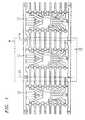
- FIG. 10illustrates an encapsulated view of the arrangement of FIG. 9, where the outer package 120 is molded to completely cover first OSA 92, first electronics 98, second OSA 102 and second electronics 108.
- package 120includes a connector receptacle 122 of the design as shown in FIG. 10.
- connector receptacle 122comprises an opening 124 of sufficient depth that first and second OSAs 92 and 102 remain exposed.
- the molding operation used to form outer package 120may simultaneously from connector receptacle 122.
- connector receptacle 122may comprises a piece part separate from outer package 120 which is subsequently clamped over package 120 to form the arrangement as illustrated in FIG. 10.
Landscapes
- Physics & Mathematics (AREA)
- General Physics & Mathematics (AREA)
- Optics & Photonics (AREA)
- Engineering & Computer Science (AREA)
- Microelectronics & Electronic Packaging (AREA)
- Power Engineering (AREA)
- Computer Hardware Design (AREA)
- Condensed Matter Physics & Semiconductors (AREA)
- Electromagnetism (AREA)
- Optical Couplings Of Light Guides (AREA)
- Optical Communication System (AREA)
- Led Device Packages (AREA)
- Light Receiving Elements (AREA)
Description
- The present invention relates to optical packaging technology and, more particularly, to a molded optical packaging arrangement.
- There exist many different arrangements for packaging optical communication arrangements. For example, the optical device (e.g., laser, LED or photodiode) may be attached to a mount which is subsequently aligned with and attached to a base member, the base member including lensing elements to facilitate coupling of an optical fiber to the optical device. In most cases, the base member will include a spherical lensing element to maximize the optical coupling. The arrangement of the mounted optical device, base member and lens is often referred to in the art as an optical subassembly, or OSA. The electronics required for operating the optical device (a driver circuit for a transmitter, or an amplification and decision circuit for a receiver, for example) may then be separately assembled (on a printed wiring board, for example) and connected to the optical subassembly by conventional electrical leads. Alternatively, the electronics may be fully enclosed in a separate housing, with only the leads exposed for connection to the optical subassembly. An advantage of using separate housings for the electronics and optics relates to the ability to interchange the components as required for different applications. For example, a data link application may operate with TTL electronic signals, and another application (with the same optics) may utilize ECL electronic signals. Additionally, if either the electrical or optical portion of an arrangement were to experience a failure, the working portion could be disconnected and re-used with another arrangement. A major disadvantage of separate packaging is the overall size of the resultant arrangement. With two separate packages, or an optical package mounted on a printed wiring board, the arrangement requires a rather large space. Further, such an arrangement is susceptible to electrical noise introduced by the necessarily long lead lengths between the electronics and the optical device. The electrical noise factor becomes a significant concern at bit rates exceeding approximately 10Mb/s. Also, long leads may limit the maximum bit rate of either a transmitter or receiver, due to parasitic lead inductance (limits transmitter) or parasitic capacitances (limits receiver).
- These and other concerns have led to the development of package designs which provide for the electronics and optical device to be housed in the same unit. Many of these unitary packages are relatively expensive, as a result of using a hybrid integrated circuit (HIC) arrangement for the electronics, with an optical subassembly attached to the HIC. Additionally, the piece parts used in the optical subassembly associated with these packages are often formed of machined metallic components, adding to the cost of the system. Further, these optical subassemblies have been known to experience alignment difficulties. Fabrication problems may also exist with respect to mating the various piece parts (i.e., outer housing, optical subassembly and HIC). Lastly, in many instances, the packaging processes for a transmitter and receiver are often very distinct, leading to manufacturing problems and increasing the overall expense of the packages system.
- An improved package design is disclosed in U. S. Patent 4,911,519 issued to W. H. Burton et al. on March 27, 1990. In the disclosed arrangement, the HIC of a conventional package is replaced by a conventional 16-pin dual-in-line package (DIP) which includes a specialized pair of end prong leads for attachment to the optical subassembly. The DIP and optical subassembly are subsequently assembled within a plastic molded package frame. The plastic molded frame is configured to include a molded optical connector receptacle for subsequent attachment of a connectorized optical fiber. The arrangement is subsequently covered with a metallic lid which is grounded to the package floor. A significant savings is realized by the utilization of the DIP, as well as the molded plastic piece part of the frame/connector assembly.
- Although the Burton et al. arrangement is considered to be a significant advance over the prior art, the need remains to further simplify optical packaging techniques, with respect to limiting the number of separate assembly operations, in light of rapidly growing markets which will require many thousands of such devices in as a cost-competitive arrangement as possible.
- GB-A- 2 229 857 discloses an optical communication arrangement according to the preamble of
claim 1. - The need remaining in the prior art is addressed by the present invention which relates to optical packaging and, more particularly, to a molded optical packaging arrangement.
- According to the present invention, there is provided an arrangement as defined in
claim 1 or 7. - In accordance with an exemplary embodiment of the present invention, a leadframe section is utilized for the placement and attachment of the electrical circuitry required to operate the associated optical device (e.g., a driver circuit for a transmitter and/or an amplifier and decision circuit for a receiver). A first molding operation is then performed to encapsulate the electronics. A support member is also molded during this step, where the support member is used for the later placement of the base member of an optical subassembly. Subsequent to the first molding operation, an optical device and associated base member are positioned with and attached to the encapsulated electronics. The combination of the electronics and optics is then encapsulated during a second molding operation to form the final packaged arrangement.
- In an alternative embodiment of the present invention, improved EMI shielding may be provided by utilizing a metallic plate which is disposed over and electrically coupled to the encapsulated electronics. The shield plate is attached to the arrangement prior to the final encapsulation step.
- An exemplary arrangement of the present invention may utilize an optical device (and lensing element(s), if required) inserted within a conventional optical subassembly (OSA), where the electrical leads exiting the optical device are connected to the leadframe and the base member portion of the OSA rests upon the molded support member. The base member, which houses a lensing element (for example, a spherical lens, fiber stub, or any other arrangement suitable for providing optical coupling), may be formed to include a receptacle portion required for the physical attachment of a connectorized fiber to the package. Alternatively, the final molding for encapsulating the optics and electronics may be designed to provide the connector receptacle as a part of the final molded outer package.
- In an alternative arrangement, the optical device (for example, a lensed LED) may be physically attached to the leadframe. In particular, the leadframe may be configured to comprise a paddle-like lead for attachment thereto of a first major surface of the optical device. The paddle includes an aperture aligned with the active region of the optical device so as to allow for the passage of the optical signal through the leadframe. A second lead is used to provide the remaining electrical attachment to the opposing major surface of the optical device. For this arrangement, a base member, positioned in the support member, includes a lensing element to facilitate coupling of the optical signal between the optical device and an attached fiber. The base member may be configured to include a connector receptacle. Alternatively, the final outer package may be molded to include the required receptacle.
- Referring now to the drawings, where like numerals represent like parts in several views:
- FIG. 1 illustrates an exemplary lead arrangement suitable for use in association with the teachings of the present invention;
- FIG. 2 illustrates a portion of the leadframe of FIG. 1 illustrating the attachment thereto of the electronics associated with a particular embodiment of the present invention;
- FIG. 3 illustrates the arrangement of FIG. 2 subsequent to the first encapsulation, including the formation of the support member;
- FIG. 4 illustrates the arrangement of FIG. 3 subsequent to the attachment thereto of an optical subassembly;
- FIG. 5 illustrates the arrangement of FIG. 4 subsequent to the final encapsulation, where the connector receptacle is molded as part of the final outer package;
- FIG. 6 illustrates an alternative arrangement of the present invention subsequent to the first encapsulation step;
- FIG. 7 illustrates the arrangement of FIG. 6 subsequent to the attachment thereto of an optical device and associated base member, the base member configured to include a connector receptacle;
- FIG. 8 illustrates the arrangement of FIG.7 subsequent to the final molding, where the receptacle portion of the base member remains exposed beyond the outer package housing;
- FIG. 9 illustrates an alternative embodiment of the present invention, prior to the final encapsulation, particularly suited for the combined packaging of a pair of optical devices such as in the formation of a molded transceiver package, where in this embodiment the optical subassemblies are formed to include a pair of connector receptacles; and
- FIG. 10 illustrates an encapsulated view of the arrangement of FIG. 9, particularly illustrating an alternative connector receptacle design.
- Referring to FIG. 1, an
exemplary leadframe 10 is illustrated which includes a large number of severable leadframe sections for use with a number of separate opto-electronic packages. It is an advantage of the present invention that the use of a leadframe structure allows for the simultaneous fabrication of a large number of opto-electronic packages, such as transmitters, receivers and/or transceivers. Similar to conventional electronic integrated circuit processing, a plurality of integrated circuits may be simultaneously attached and wirebonded alonglocations 12 ofleadframe 10. In accordance with the teachings of the present invention, the plurality of integrated circuits are simultaneously encapsulated, leaving exposed the leads required for subsequent attachments thereto. In particular, an associated plurality of optical arrangements are subsequently attached to the molded electronics and the combination of electronics and optics encapsulated to form the final package assembly. When the final molding operation is completed,leadframe 10 may be severed along dottedlines 14 to form a plurality of final package assemblies. The remaining figures illustrate a single leadframe section and the various items associated therewith. It is to be understood that the illustration of a single leadframe section is only for the sake of discussion and in general a larger number of opto-electronic assemblies are simultaneously formed in production. - A
single leadframe section 20 is particularly illustrated in FIG. 2.Section 20 includes a centralground plane paddle 22 to which anintegrated circuit 24 is attached. Integratedcircuit 24 is subsequently coupled, using wirebonds for example, to selected leads 26 ofleadframe section 20. Aseparate capacitive element 28, which may be required for certain transmitter and/or receiver configurations, is attached toleadframe section 20 as shown in FIG. 2. Subsequent to the attachment ofelectronics first housing 30, as illustrated in FIG. 3. In this particular embodiment, used for the attachment of an optical subassembly tohousing 30, a pair of end prong leads 32,34 ofleadframe section 20 remain exposed. End prong leads 32,34 may be bent upwards at an angle of, for example, 90° (as shown) to facilitate the later attachment of a pair of OSA leads. Alternatively, end prong leads 32,34 may remain in the plane ofleadframe section 20 and the OSA leads bent downward to complete the attachment. As shown in FIG. 3, the first molding operation is also used to form asupport member 36, where as discussed above, the base portion of an OSA is positioned to rest uponsupport member 36.Support member 36 has been found to improve the stability of the assembly during the subsequent molding operation. - Referring to FIG. 4, an
optical subassembly 40 is illustrated as attached to the arrangement of FIG. 3, withbase member 42 ofoptical subassembly 40 positioned to rest uponsupport member 36. Anoptical device 44 is supported on amount 46 such that electrical leads 48 ofmount 46 may be coupled to end prong leads 32,34 (FIG. 3).Base member 42 may be attached to supportmember 36 using an adhesive, such as an epoxy, or merely held in place with a mandrel. The mandrel is utilized to prevent motion ofOSA 40 and block the entry of any molding material intobase member 42 during the final molding operation. FIG. 5 illustrates a final package of the arrangement of FIG. 4. As shown,OSA 40 and encapsulatedelectronic housing 30 are completely covered with a moldedouter housing 52. For the particular embodiment of FIG. 5, base member 42 (partially shown in phantom) is completely embedded withinhousing 52 andhousing 52 is formed to include aconnector receptacle 54 aligned withbase member 42. - As mentioned above, an exemplary molding technique which may be used to form both electronic
inner package 30 and the finalouter package 52 is transfer molding, as used in conventional integrated circuit packaging. In transfer molding, a preheated charge of thermoset molding compound is moved from a dielectric preheater into the mold cavity through a single inlet port. Transfer molding, as is well-known, is best suited for the type of insert molding where it is desired to precisely form certain features, such as the connector receptacle of this particular embodiment of the present invention. During the molding process, leadframe 20 of FIG. 2 (i.e., leads 26) is clamped in place to hold the components as stationary as possible. A first, relatively simple, rectangular mold is then used to encapsulate the electronics. For the second molding operation,leadframe 20 is again clamped into place and, as mentioned above, a mandrel may be used to both prevent motion ofOSA 40 and createinner bore 53 ofreceptacle 54. For the second operation, a mold including the design ofconnector receptacle 54 is used to encapsulate both the housed electronics and the optical components. - In an alternative embodiment of the present invention, the use of a separate optical subassembly may be replaced by the direct attachment of an optical device to the leadframe associated with the electronics. FIG. 6 illustrates an exemplary encapsulated
electronic subassembly 60 including a specialized pair ofleads aperture 66. An optical device 68 (shown in phantom) is attached along a first major surface to paddle 62 such that the active region ofdevice 68 is aligned withaperture 66. Alternatively,device 68 may be attached to the opposite side ofpaddle 62 such that an aperture is not required. The remaining electrical contact todevice 68 is formed by wirebonding the opposing major surface ofdevice 68 to lead 64. - As with the arrangement described above in association with FIGs. 1-5, the arrangement of FIG. 6 requires the utilization of an optical base member to facilitate the optical coupling between
device 68 and a connected optical fiber. FIG. 7 illustrates an exemplary embodiment wherein abase member 70 is positioned upon asupport member 72 and attached to paddle 62 so as to be in optical alignment withdevice 68. In general,base member 70 may include a lensing element (e..g, spherical lens or fiber stub) to improve optical coupling. For the particular embodiment illustrated in FIG.7,base member 70 is formed to include aconnector receptacle 74. The use of a base member including a receptacle portion thus simplifies the final molding operation (i.e., no need to mold a receptacle) and ensures that the receptacle will be optically aligned with the associated optical device. FIG. 8 illustrates the arrangement of FIG. 7 subsequent to the final molding operation. As shown, the mold used for this process is configured to form anouter housing 80 such thatreceptacle portion 74 ofbase member 70 remains exposed. - An advantage of the leadframe-based packaging technology of the present invention is that any number of optical devices (and the associated encapsulated electronics) may be embedded within the same molded outer package. In general, therefore, an array-like package may be formed. In one particular embodiment, a pair of optical devices may be simultaneously encapsulated so as to form, for example, a dual-wavelength transmitter or receiver (or a sparing arrangement) or, alternatively, a transceiver including a light transmitting device (e.g., LED or laser) and a light receiving device (e.g., PIN or avalanche photodiode). FIG. 9 illustrates in particular an
exemplary transceiver package 90 formed in accordance with the teachings of the present invention. As shown in this view, a first OSA 92 (housing a light transmitting device and any required lensing elements) includes abase member 94 which rests upon afirst support member 96.OSA 92 is also electronically coupled to encapsulateddriver electronics 98.Base member 94 ofOSA 92 is formed in this particular configuration to include aconnector receptacle 100. Similarly, a second OSA 102 (housing a light receiving device and any required lensing elements) includes abase member 104 which rests upon asecond support member 106.OSA 102 is then electrically coupled to encapsulated amplifier-decision circuit electronics 108. In order to reduce the effects of electromagnetic interference (EMI) on the operation ofelectronics 108, ametallic plate 110 may be disposed overpackage 108 and coupled to the groundplane exiting package 108 to form an EMI shield.Plate 110 may comprise a separate piece of metal which is attached to the leadframe subsequent to the first molding operation (i.e., encapsulation of the electronics). Alternatively, the leadframe utilized for this embodiment may be formed to include a plate portion which may be bent over the packaged electronics to form the shield. - FIG. 10 illustrates an encapsulated view of the arrangement of FIG. 9, where the
outer package 120 is molded to completely coverfirst OSA 92,first electronics 98,second OSA 102 andsecond electronics 108. In this particular embodiment,package 120 includes aconnector receptacle 122 of the design as shown in FIG. 10. In particular,connector receptacle 122 comprises anopening 124 of sufficient depth that first andsecond OSAs outer package 120 may simultaneously fromconnector receptacle 122. Alternatively,connector receptacle 122 may comprises a piece part separate fromouter package 120 which is subsequently clamped overpackage 120 to form the arrangement as illustrated in FIG. 10.
Claims (11)
- An optical communication arrangement for use with an associated optical fiber, the arrangement comprising:a semiconductor optical device (44; 68);electronic circuitry (24), required for the operation of said semiconductor optical device;a leadframe (12), to which the electronic circuitry is attached;first molded packaging (30, 36; 60, 72) comprising at least a first section (30; 60) encapsulating said electronic circuitry and an associated portion of said leadframe;an optical coupling means (42, 46; 70) comprising at least a base member (42; 70), for facilitating optical coupling between said semiconductor optical device and the associated optical fiber; andsecond molded packaging (52; 80) substantially encapsulating the encapsulated electronic circuitry, the semiconductor optical device, and the base member, whilst enabling an optical access to said semiconductor optical device,CHARACTERISED IN THATthe first molded packaging (30, 36; 60, 72) further comprises a second section (36; 72) encapsulating a portion of said leadframe separate from that encapsulated by the first section, said second section (36; 72) being also encapsulated by said second molded packaging (52; 80) and shaped so as to form a molded support member,the base member (42; 70) is disposed to rest upon said molded support member (36; 72), andthe semiconductor device (44; 68) is attached, either to a portion of the leadframe not encapsulated by the first molded packaging, or to said optical coupling means.
- An optical arrangement as defined in claim 1, further comprising connector receptacle means (42;54;74) for facilitating attachment of the associated optical fiber to said arrangement.
- An arrangement as defined in claim 2, wherein the second molded packaging (52) is formed to include the connector receptacle means (54) and the base member (42) remains substantially embedded within said second molded packaging; or
the base member (70) is formed to include the connector receptacle (74) and the second molded packaging (80) is formed such that the connector receptacle portion of said base member remains exposed. - An arrangement as defined in claim 1, wherein said optical coupling means (42,46) further comprises a mounting member (46) attached to said base member (42) and supporting said optical device (44), and
said optical device (44) comprises an optical transmitting device or an optical receiving device. - An arrangement as defined in claim 1, wherein the arrangement further comprises EMI shielding means (110) disposed over the first molded packaging and electrically coupled to the leadframe.
- An arrangement as defined in claim 1, wherein the first and second molded packaging comprise a transfer-molded plastic material.
- An optical communication arrangement for use with a pair of associated optical fibers, the arrangement comprising:a leadframe (12);a first semiconductor optical device;first electronic circuitry (98), required for the operation of said first semiconductor optical device, attached to said leadframe;a second semiconductor optical device;second electronic circuitry (108), required for the operation of said second semiconductor optical device, attached to said leadframe at a location physically separate from said first electronic circuitry;first molded packaging comprising a first section encapsulating said first electronic circuitry and an associated portion of said leadframe, and a second section (96) encapsulating a separate portion of said leadframe and shaped so as to form a first molded support member;second molded packaging comprising a first section encapsulating said second electronic circuitry and an associated portion of said leadframe, and a second section (106) encapsulating a further separate portion of said leadframe and shaped so as to form a second molded support member;first optical coupling means (92), including a first base member (94) disposed to rest upon said first molded support member (96), for facilitating optical coupling between said first semiconductor optical device and a first one of the pair of associated optical fibers, said first semiconductor device being attached, either to a portion of the leadframe not encapsulated by the first and second molded packaging, or to said first optical coupling means;second optical coupling means (102), including a second base member (104) disposed to rest upon said second molded support member (106), for facilitating optical coupling between said second semiconductor optical device and the second one of the pair of associated optical fibers, said second semiconductor device being attached, either to a portion of the leadframe not encapsulated by the first and second molded packaging, or to said second optical coupling means; andthird molded packaging (120) substantially encapsulating the first and second molded packaging, the first and second semiconductor optical device, and the first and second optical coupling means, whilst enabling an optical access to said first and second semiconductor optical device.
- An arrangement as defined in claim 7, further comprisingfirst connector receptacle means (100) for facilitating attachment of the associated first optical fiber to said arrangement; andsecond connector receptacle means (104) for facilitating attachment of the associated second optical fiber to said arrangement.
- An arrangement as defined in claim 8, whereinthe first base member (94) is formed to include the first connector receptacle means (100); andthe second base member (104) is formed to include the second connector receptacle means, wherein the third molded packaging (120) is formed such that the connector receptacle portions of the first and second base members remain exposed.
- An arrangement as defined in claim 7, wherein the arrangement further comprises EMI shielding means (110) disposed over the first or the second molded packaging.
- An arrangement as defined in claim 7 wherein the first, second and third molded packagings comprise a transfer-molded plastic.
Applications Claiming Priority (2)
| Application Number | Priority Date | Filing Date | Title |
|---|---|---|---|
| US691649 | 1991-04-25 | ||
| US07/691,649US5113466A (en) | 1991-04-25 | 1991-04-25 | Molded optical packaging arrangement |
Publications (3)
| Publication Number | Publication Date |
|---|---|
| EP0510860A2 EP0510860A2 (en) | 1992-10-28 |
| EP0510860A3 EP0510860A3 (en) | 1993-03-10 |
| EP0510860B1true EP0510860B1 (en) | 1997-07-02 |
Family
ID=24777389
Family Applications (1)
| Application Number | Title | Priority Date | Filing Date |
|---|---|---|---|
| EP92303310AExpired - LifetimeEP0510860B1 (en) | 1991-04-25 | 1992-04-14 | Molded optical packaging arrangement |
Country Status (6)
| Country | Link |
|---|---|
| US (1) | US5113466A (en) |
| EP (1) | EP0510860B1 (en) |
| JP (1) | JP2698285B2 (en) |
| KR (1) | KR960014128B1 (en) |
| CA (1) | CA2062413C (en) |
| DE (1) | DE69220613T2 (en) |
Cited By (1)
| Publication number | Priority date | Publication date | Assignee | Title |
|---|---|---|---|---|
| DE10001873B4 (en)* | 2000-01-18 | 2010-06-02 | Avago Technologies Fiber Ip (Singapore) Pte. Ltd. | Optical transmitting and receiving device |
Families Citing this family (58)
| Publication number | Priority date | Publication date | Assignee | Title |
|---|---|---|---|---|
| US5155786A (en)* | 1991-04-29 | 1992-10-13 | International Business Machines Corporation | Apparatus and a method for an optical fiber interface |
| US5241614A (en)* | 1991-04-29 | 1993-08-31 | International Business Machines Corporation | Apparatus and a method for an optical fiber interface |
| EP0582992B1 (en)* | 1992-08-11 | 1998-06-03 | Sumitomo Electric Industries, Ltd | Optical module with improved grounding of an optical element |
| US5337398A (en)* | 1992-11-30 | 1994-08-09 | At&T Bell Laboratories | Single in-line optical package |
| US5416871A (en)* | 1993-04-09 | 1995-05-16 | Sumitomo Electric Industries, Ltd. | Molded optical connector module |
| US5345524A (en)* | 1993-05-20 | 1994-09-06 | Motorola, Inc. | Optoelectronic transceiver sub-module and method for making |
| US5432878A (en)* | 1994-03-03 | 1995-07-11 | Cts Corporation | Silicon carrier for testing and alignment of optoelectronic devices and method of assembling same |
| USRE40150E1 (en) | 1994-04-25 | 2008-03-11 | Matsushita Electric Industrial Co., Ltd. | Fiber optic module |
| SE9402082L (en)* | 1994-06-14 | 1995-12-15 | Ericsson Telefon Ab L M | Miniature optical capsule |
| US5717533A (en) | 1995-01-13 | 1998-02-10 | Methode Electronics Inc. | Removable optoelectronic module |
| US6220878B1 (en) | 1995-10-04 | 2001-04-24 | Methode Electronics, Inc. | Optoelectronic module with grounding means |
| US6354747B1 (en) | 1996-08-26 | 2002-03-12 | Sumitomo Electric Industries, Ltd. | Optical module |
| EP0826997B1 (en)* | 1996-08-26 | 2003-07-23 | Sumitomo Electric Industries, Ltd. | Optoelectronic module and method of manufacturing the same |
| JP2002514312A (en)* | 1996-10-22 | 2002-05-14 | スチュワート コネクター システムズ インコーポレーテッド | Optical interconnect system |
| JP2002508884A (en)* | 1996-10-23 | 2002-03-19 | ユニフェイズ オプト ホールディングス インコーポレイテッド | Electro-optical device, cage suitable for using the device, and method of manufacturing the device |
| JP3514609B2 (en)* | 1997-05-29 | 2004-03-31 | 新光電気工業株式会社 | Lead frame for optical semiconductor device and optical semiconductor device |
| SG71172A1 (en) | 1997-12-03 | 2000-03-21 | Sumitomo Electric Industries | Optical data link |
| US6239427B1 (en)* | 1998-01-14 | 2001-05-29 | Sumitomo Electric Industries, Ltd. | Optical data link |
| US6315465B1 (en)* | 1998-12-21 | 2001-11-13 | Sumitomo Electric Industries, Ltd. | Optical module |
| US6366380B1 (en) | 1999-02-12 | 2002-04-02 | Cisco Technology, Inc | Optical transceiver EMI detuning device |
| US6901221B1 (en) | 1999-05-27 | 2005-05-31 | Jds Uniphase Corporation | Method and apparatus for improved optical elements for vertical PCB fiber optic modules |
| US6213651B1 (en) | 1999-05-26 | 2001-04-10 | E20 Communications, Inc. | Method and apparatus for vertical board construction of fiber optic transmitters, receivers and transceivers |
| US6220873B1 (en) | 1999-08-10 | 2001-04-24 | Stratos Lightwave, Inc. | Modified contact traces for interface converter |
| US6285324B1 (en) | 1999-09-15 | 2001-09-04 | Lucent Technologies Inc. | Antenna package for a wireless communications device |
| US6325551B1 (en) | 1999-12-08 | 2001-12-04 | New Focus, Inc. | Method and apparatus for optically aligning optical fibers with optical devices |
| US6632029B1 (en) | 1999-12-22 | 2003-10-14 | New Focus, Inc. | Method & apparatus for packaging high frequency components |
| US6704515B1 (en)* | 1999-12-30 | 2004-03-09 | The Boeing Company | Fiber optic interface module and associated fabrication method |
| US6607308B2 (en) | 2001-02-12 | 2003-08-19 | E20 Communications, Inc. | Fiber-optic modules with shielded housing/covers having mixed finger types |
| US6659655B2 (en) | 2001-02-12 | 2003-12-09 | E20 Communications, Inc. | Fiber-optic modules with housing/shielding |
| JP4543561B2 (en)* | 2001-02-19 | 2010-09-15 | 住友電気工業株式会社 | Optical module manufacturing method and optical module |
| JP2003332590A (en)* | 2002-05-14 | 2003-11-21 | Sumitomo Electric Ind Ltd | Optical module and optical transceiver module |
| DE10322071A1 (en)* | 2003-05-15 | 2004-09-02 | Infineon Technologies Ag | Micro-optical module, has housing formed as molded interconnect device, with three-dimensional conductor structure for connecting optoelectronic circuitry with components |
| US7268368B1 (en) | 2003-08-29 | 2007-09-11 | Standard Microsystems Corporation | Semiconductor package having optical receptacles and light transmissive/opaque portions and method of making same |
| JP4170950B2 (en)* | 2003-10-10 | 2008-10-22 | 松下電器産業株式会社 | Optical device and manufacturing method thereof |
| US7805084B2 (en)* | 2004-05-20 | 2010-09-28 | Finisar Corporation | Dual stage modular optical devices |
| US20060153507A1 (en)* | 2004-05-21 | 2006-07-13 | Togami Chris K | Modular optical devices compatible with legacy form factors |
| US20050265650A1 (en)* | 2004-05-27 | 2005-12-01 | Sunil Priyadarshi | Small profile, pluggable optical transceiver subassembly |
| US7795695B2 (en) | 2005-01-27 | 2010-09-14 | Analog Devices, Inc. | Integrated microphone |
| US7449356B2 (en)* | 2005-04-25 | 2008-11-11 | Analog Devices, Inc. | Process of forming a microphone using support member |
| US20070071268A1 (en)* | 2005-08-16 | 2007-03-29 | Analog Devices, Inc. | Packaged microphone with electrically coupled lid |
| US7825484B2 (en)* | 2005-04-25 | 2010-11-02 | Analog Devices, Inc. | Micromachined microphone and multisensor and method for producing same |
| US7885423B2 (en)* | 2005-04-25 | 2011-02-08 | Analog Devices, Inc. | Support apparatus for microphone diaphragm |
| US7258495B1 (en) | 2005-06-24 | 2007-08-21 | Corning Incorporated | Lensed fiber stub assemblies optical and optoelectronic packages including them |
| US20070040231A1 (en)* | 2005-08-16 | 2007-02-22 | Harney Kieran P | Partially etched leadframe packages having different top and bottom topologies |
| WO2007024909A1 (en)* | 2005-08-23 | 2007-03-01 | Analog Devices, Inc. | Multi-microphone system |
| US7961897B2 (en) | 2005-08-23 | 2011-06-14 | Analog Devices, Inc. | Microphone with irregular diaphragm |
| WO2008003051A2 (en)* | 2006-06-29 | 2008-01-03 | Analog Devices, Inc. | Stress mitigation in packaged microchips |
| EP2044802B1 (en)* | 2006-07-25 | 2013-03-27 | Analog Devices, Inc. | Multiple microphone system |
| US20080175425A1 (en)* | 2006-11-30 | 2008-07-24 | Analog Devices, Inc. | Microphone System with Silicon Microphone Secured to Package Lid |
| US7694610B2 (en)* | 2007-06-27 | 2010-04-13 | Siemens Medical Solutions Usa, Inc. | Photo-multiplier tube removal tool |
| JP5412069B2 (en)* | 2008-07-30 | 2014-02-12 | 矢崎総業株式会社 | Female optical connector and manufacturing method of female optical connector |
| EP2265102B1 (en)* | 2009-06-19 | 2014-06-25 | Baumer Innotec AG | Sensor device without housing |
| US8632261B2 (en)* | 2010-04-20 | 2014-01-21 | Hon Hai Precision Industry Co., Ltd. | Integrated and sealed opto-electronic device assembly |
| US9676614B2 (en) | 2013-02-01 | 2017-06-13 | Analog Devices, Inc. | MEMS device with stress relief structures |
| US10167189B2 (en) | 2014-09-30 | 2019-01-01 | Analog Devices, Inc. | Stress isolation platform for MEMS devices |
| US10131538B2 (en) | 2015-09-14 | 2018-11-20 | Analog Devices, Inc. | Mechanically isolated MEMS device |
| US11417611B2 (en) | 2020-02-25 | 2022-08-16 | Analog Devices International Unlimited Company | Devices and methods for reducing stress on circuit components |
| US11981560B2 (en) | 2020-06-09 | 2024-05-14 | Analog Devices, Inc. | Stress-isolated MEMS device comprising substrate having cavity and method of manufacture |
Family Cites Families (15)
| Publication number | Priority date | Publication date | Assignee | Title |
|---|---|---|---|---|
| US4307934A (en)* | 1978-05-08 | 1981-12-29 | General Dynamics, Pomona Division | Packaged fiber optic modules |
| JPS55129307A (en)* | 1979-02-06 | 1980-10-07 | Texas Instruments Inc | Self matching fiberroptical package |
| DE3175956D1 (en)* | 1980-11-28 | 1987-04-09 | Toshiba Kk | Module for a fiber optic link |
| DE3172553D1 (en)* | 1980-11-28 | 1985-11-07 | Toshiba Kk | Method for manufacturing a module for a fiber optic link |
| US4798440A (en)* | 1983-01-24 | 1989-01-17 | Amp Incorporated | Fiber optic connector assembly |
| JPS59136610U (en)* | 1983-03-02 | 1984-09-12 | 富士通株式会社 | optical connector |
| US4633582A (en)* | 1985-08-14 | 1987-01-06 | General Instrument Corporation | Method for assembling an optoisolator and leadframe therefor |
| US4803361A (en)* | 1986-05-26 | 1989-02-07 | Hitachi, Ltd. | Photoelectric device with optical fiber and laser emitting chip |
| US4752109A (en)* | 1986-09-02 | 1988-06-21 | Amp Incorporated | Optoelectronics package for a semiconductor laser |
| US4911519A (en)* | 1989-02-01 | 1990-03-27 | At&T Bell Laboratories | Packaging techniques for optical transmitters/receivers |
| CA1330576C (en)* | 1989-03-29 | 1994-07-05 | Camilo M. Tabalba | Transient voltage suppression for electro-optic modules |
| US4913511A (en)* | 1989-03-30 | 1990-04-03 | Northern Telecom Limited | Transient voltage suppression for electro-optic modules |
| GB2229857B (en)* | 1989-03-31 | 1992-12-23 | Stc Plc | Semiconductor device package |
| JP2881806B2 (en)* | 1989-04-12 | 1999-04-12 | 住友電気工業株式会社 | Optical module and manufacturing method thereof |
| AU646223B2 (en)* | 1989-05-19 | 1994-02-17 | Bt&D Technologies Limited | Housing for an opto-electronic device |
- 1991
- 1991-04-25USUS07/691,649patent/US5113466A/ennot_activeExpired - Lifetime
- 1992
- 1992-03-06CACA002062413Apatent/CA2062413C/ennot_activeExpired - Lifetime
- 1992-04-14EPEP92303310Apatent/EP0510860B1/ennot_activeExpired - Lifetime
- 1992-04-14DEDE69220613Tpatent/DE69220613T2/ennot_activeExpired - Lifetime
- 1992-04-20KRKR1019920006586Apatent/KR960014128B1/ennot_activeExpired - Fee Related
- 1992-04-22JPJP4127975Apatent/JP2698285B2/ennot_activeExpired - Lifetime
Cited By (1)
| Publication number | Priority date | Publication date | Assignee | Title |
|---|---|---|---|---|
| DE10001873B4 (en)* | 2000-01-18 | 2010-06-02 | Avago Technologies Fiber Ip (Singapore) Pte. Ltd. | Optical transmitting and receiving device |
Also Published As
| Publication number | Publication date |
|---|---|
| KR960014128B1 (en) | 1996-10-14 |
| DE69220613T2 (en) | 1998-01-29 |
| KR920020227A (en) | 1992-11-20 |
| DE69220613D1 (en) | 1997-08-07 |
| CA2062413A1 (en) | 1992-10-26 |
| US5113466A (en) | 1992-05-12 |
| JPH07193262A (en) | 1995-07-28 |
| CA2062413C (en) | 1997-08-05 |
| EP0510860A2 (en) | 1992-10-28 |
| EP0510860A3 (en) | 1993-03-10 |
| JP2698285B2 (en) | 1998-01-19 |
Similar Documents
| Publication | Publication Date | Title |
|---|---|---|
| EP0510860B1 (en) | Molded optical packaging arrangement | |
| US5123066A (en) | Molded optical package utilizing leadframe technology | |
| EP0600645B1 (en) | Single in-line optical package | |
| EP0381370B1 (en) | Improved packaging techniques for optical transmitters/receivers | |
| EP0437931B1 (en) | Packaging for a pair of optical devices | |
| US5280191A (en) | Lightwave packaging for pairs of optical devices having thermal dissipation means | |
| US6712527B1 (en) | Fiber optic connections and method for using same | |
| US6137158A (en) | Leadframe and leadframe assembly for parallel optical computer link | |
| US6572280B2 (en) | Optical transmitting/receiving module including an internal optical waveguide | |
| US5432630A (en) | Optical bus with optical transceiver modules and method of manufacture | |
| US5101465A (en) | Leadframe-based optical assembly | |
| US6733189B2 (en) | Electrooptical transmitting/receiving module, and method for producing the module | |
| US6234686B1 (en) | Optical data link | |
| US8031992B2 (en) | Optoelectronic module and method for producing an optoelectronic module | |
| US6565267B2 (en) | Optical transmitting device and optical receiving device each having receptacle type optical module | |
| US7036999B2 (en) | Optoelectronic module and optoelectronic system | |
| KR970002933Y1 (en) | Molded optical package utilizing leadframe technology | |
| JP3674019B2 (en) | Optical link device |
Legal Events
| Date | Code | Title | Description |
|---|---|---|---|
| PUAI | Public reference made under article 153(3) epc to a published international application that has entered the european phase | Free format text:ORIGINAL CODE: 0009012 | |
| AK | Designated contracting states | Kind code of ref document:A2 Designated state(s):DE FR GB | |
| PUAL | Search report despatched | Free format text:ORIGINAL CODE: 0009013 | |
| AK | Designated contracting states | Kind code of ref document:A3 Designated state(s):DE FR GB | |
| 17P | Request for examination filed | Effective date:19930826 | |
| RAP3 | Party data changed (applicant data changed or rights of an application transferred) | Owner name:AT&T CORP. | |
| 17Q | First examination report despatched | Effective date:19950119 | |
| GRAG | Despatch of communication of intention to grant | Free format text:ORIGINAL CODE: EPIDOS AGRA | |
| GRAH | Despatch of communication of intention to grant a patent | Free format text:ORIGINAL CODE: EPIDOS IGRA | |
| GRAH | Despatch of communication of intention to grant a patent | Free format text:ORIGINAL CODE: EPIDOS IGRA | |
| GRAA | (expected) grant | Free format text:ORIGINAL CODE: 0009210 | |
| AK | Designated contracting states | Kind code of ref document:B1 Designated state(s):DE FR GB | |
| REF | Corresponds to: | Ref document number:69220613 Country of ref document:DE Date of ref document:19970807 | |
| ET | Fr: translation filed | ||
| PLBE | No opposition filed within time limit | Free format text:ORIGINAL CODE: 0009261 | |
| STAA | Information on the status of an ep patent application or granted ep patent | Free format text:STATUS: NO OPPOSITION FILED WITHIN TIME LIMIT | |
| 26N | No opposition filed | ||
| PGFP | Annual fee paid to national office [announced via postgrant information from national office to epo] | Ref country code:FR Payment date:20010322 Year of fee payment:10 | |
| REG | Reference to a national code | Ref country code:GB Ref legal event code:IF02 | |
| PG25 | Lapsed in a contracting state [announced via postgrant information from national office to epo] | Ref country code:FR Free format text:LAPSE BECAUSE OF NON-PAYMENT OF DUE FEES Effective date:20021231 | |
| REG | Reference to a national code | Ref country code:FR Ref legal event code:ST | |
| PGFP | Annual fee paid to national office [announced via postgrant information from national office to epo] | Ref country code:DE Payment date:20110421 Year of fee payment:20 | |
| PGFP | Annual fee paid to national office [announced via postgrant information from national office to epo] | Ref country code:GB Payment date:20110421 Year of fee payment:20 | |
| REG | Reference to a national code | Ref country code:DE Ref legal event code:R071 Ref document number:69220613 Country of ref document:DE | |
| REG | Reference to a national code | Ref country code:DE Ref legal event code:R071 Ref document number:69220613 Country of ref document:DE | |
| REG | Reference to a national code | Ref country code:GB Ref legal event code:PE20 Expiry date:20120413 | |
| PG25 | Lapsed in a contracting state [announced via postgrant information from national office to epo] | Ref country code:DE Free format text:LAPSE BECAUSE OF EXPIRATION OF PROTECTION Effective date:20120415 | |
| PG25 | Lapsed in a contracting state [announced via postgrant information from national office to epo] | Ref country code:GB Free format text:LAPSE BECAUSE OF EXPIRATION OF PROTECTION Effective date:20120413 |