EP0508459B1 - Digital transmission test system - Google Patents
Digital transmission test systemDownload PDFInfo
- Publication number
- EP0508459B1 EP0508459B1EP92106251AEP92106251AEP0508459B1EP 0508459 B1EP0508459 B1EP 0508459B1EP 92106251 AEP92106251 AEP 92106251AEP 92106251 AEP92106251 AEP 92106251AEP 0508459 B1EP0508459 B1EP 0508459B1
- Authority
- EP
- European Patent Office
- Prior art keywords
- data
- digital
- display
- signal
- test system
- Prior art date
- Legal status (The legal status is an assumption and is not a legal conclusion. Google has not performed a legal analysis and makes no representation as to the accuracy of the status listed.)
- Expired - Lifetime
Links
- 238000012360testing methodMethods0.000titleclaimsdescription40
- 230000005540biological transmissionEffects0.000titleclaimsdescription31
- 238000012545processingMethods0.000claimsdescription7
- 230000008054signal transmissionEffects0.000claimsdescription6
- 238000000034methodMethods0.000description12
- 230000007704transitionEffects0.000description3
- 230000000007visual effectEffects0.000description3
- 230000000295complement effectEffects0.000description2
- 230000006866deteriorationEffects0.000description1
- 238000010586diagramMethods0.000description1
- 230000007257malfunctionEffects0.000description1
- 238000004519manufacturing processMethods0.000description1
- 238000012544monitoring processMethods0.000description1
- 238000001228spectrumMethods0.000description1
- 238000010561standard procedureMethods0.000description1
Images


Classifications
- H—ELECTRICITY
- H04—ELECTRIC COMMUNICATION TECHNIQUE
- H04N—PICTORIAL COMMUNICATION, e.g. TELEVISION
- H04N17/00—Diagnosis, testing or measuring for television systems or their details
- H—ELECTRICITY
- H04—ELECTRIC COMMUNICATION TECHNIQUE
- H04N—PICTORIAL COMMUNICATION, e.g. TELEVISION
- H04N17/00—Diagnosis, testing or measuring for television systems or their details
- H04N17/004—Diagnosis, testing or measuring for television systems or their details for digital television systems
- H—ELECTRICITY
- H04—ELECTRIC COMMUNICATION TECHNIQUE
- H04N—PICTORIAL COMMUNICATION, e.g. TELEVISION
- H04N21/00—Selective content distribution, e.g. interactive television or video on demand [VOD]
- H04N21/20—Servers specifically adapted for the distribution of content, e.g. VOD servers; Operations thereof
- H04N21/23—Processing of content or additional data; Elementary server operations; Server middleware
- H04N21/234—Processing of video elementary streams, e.g. splicing of video streams or manipulating encoded video stream scene graphs
- H04N21/2347—Processing of video elementary streams, e.g. splicing of video streams or manipulating encoded video stream scene graphs involving video stream encryption
- H—ELECTRICITY
- H04—ELECTRIC COMMUNICATION TECHNIQUE
- H04N—PICTORIAL COMMUNICATION, e.g. TELEVISION
- H04N21/00—Selective content distribution, e.g. interactive television or video on demand [VOD]
- H04N21/40—Client devices specifically adapted for the reception of or interaction with content, e.g. set-top-box [STB]; Operations thereof
- H04N21/43—Processing of content or additional data, e.g. demultiplexing additional data from a digital video stream; Elementary client operations, e.g. monitoring of home network or synchronising decoder's clock; Client middleware
- H04N21/44—Processing of video elementary streams, e.g. splicing a video clip retrieved from local storage with an incoming video stream or rendering scenes according to encoded video stream scene graphs
- H04N21/4405—Processing of video elementary streams, e.g. splicing a video clip retrieved from local storage with an incoming video stream or rendering scenes according to encoded video stream scene graphs involving video stream decryption
Definitions
- the present inventionrelates to a digital transmission test system suitable for checking digital signal transmission systems.
- EP 0 138 613 A2is described a method and apparatus for monitoring suitability of a transmission path for transmission of digital data by transmitting a test signal over the transmission path.
- the test signalis composed of a succession of video signal lines each including a horizontal sync pulse and a pattern of digital 1's and 0's at a predetermined frequency and occurring on each line at the same data position relative to the horizontal sync pulse.
- the patternscomprise a reference pattern of alternating 1's and 0's and test pattern of 1's and 0's at random or in a sequence known to be disruptive to the transmission path.
- the test signalis received and is displayed on a waveform monitor with the reference pattern and the test pattern interleaved with the complement of the reference pattern and complement of the test pattern, so that the four patterns are superimposed and enclose a generally eye-shaped area.
- DE 36 01 605 Adiscloses a digital transmission test signal generating circuit, wherein a quasi-statistic bit pattern is used as a digital test signal to be transmitted during the lines 25 to 312 and 338 to 625 of first and second fields and displayed at the decoder output in the form of quasi-statistic colour pattern on a TV monitor screen.
- the SMPTESociety of Motion Picture and Television Engineers, Inc.
- NRZIno-return-to-zero inverted code
- AGCautomatic gain control
- a digital video transmission test systemincluding encoding means for encoding digital data, a transmission path for transmitting the encoded data, decoding means for recovering digital data from the transmitted data, a display for displaying the recovered data and a test signal generating circuit for generating and supplying a digital test signal to the encoding means, characterized in that said display is a monitor TV set and the test system further includes processing means for processing the transmitted data by means of controlling at least one signal parameter of the transmitted data and timing means for controlling said generating circuit in such a manner that said data will occur in the duration corresponding to a first predetermined area of said display, and in that the digital test signal is formed by a repeated first bit pattern which is with the respect to the controlled signal parameter the worst case of possible bit pattern forming digital data to be transmitted.
- the transmission systemfunctions normally, the data having passed therethrough cause an image with particular brightness and color to be displayed in particular areas of the screen. If the transmission system fails to function normally, the data acquire an error during passage therethrough and produce changes in the image displayed in those particular areas of the screen. This makes it possible to check the target transmission system for performance with the worst-case data in an easy, visual manner without recourse to special measuring instruments.
- the embodimentconstitutes a circuit arrangement for checking a transmission system that transmits digital video data under the scrambled NRZI method.
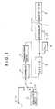
- Fig. 1digital video data DTV fed to a terminal 1 are forwarded to the "a" side fixed terminal of a changeover switch 2.
- the "b" side fixed terminal of the changeover switch 2is supplied with a test signal DTE from a test signal generating circuit 3.
- the test signal DTEcomprises two combinations of alternately repeated 10-bit hexadecimal data.
- One data combinationis made of "300” and “198” continuing alternately for display on the upper part of the screen, and the other combination is constituted by "110" and "200” continuing alternately for display on the lower part of the screen.
- the output data from the changeover switch 2are fed to a scrambler 4.
- the dataAfter being scrambled by the scrambler 4, the data are forwarded over a transmission path 5 to a circuit 6 comprising an AGC part and a equalizer part.
- the AGC partcontrols gain in such a way that keeps the level of the transmitted data constant.
- the equalizer partcorrects the high and low frequency characteristics that were deteriorated during transmission, whereby the inter-symbol interference involved is suppressed.
- the output data from the circuit 6are supplied to both a descrambler 7 and a PLL circuit 8.
- the PLL circuit 8reproduces the clock signal that is sent to the descrambler 7.
- the descrambler 7descrambles the received data by performing a module-2 multiplication thereon using the above polynomial.
- the descramblingtakes place in synchronism with the clock signal CLK.
- the dataAfter being descrambled by the descrambler 7, the data are supplied to a monitor TV set 9.
- the changeover switch 2is first placed in the "a" position. This causes the scrambler 4 to scramble the digital video data DTV.
- the scrambled dataare sent over the transmission path 5 and through the circuit 6 to the descrambler 7.
- the descrambler 7outputs the descrambled digital video data DTV to the monitor TV set 9.
- the screen of the monitor TV set 9displays the image produced by the received digital video data DTV.
- the scrambler 4scrambles the test signal DTE.
- the test signal DTE corresponding to the upper part of the screenis the combination of hexadecimal 10-bit data "300" and "198" continuing alternately.
- the scrambled datadevelop a DC component (see Fig. 5 (B)), which constitutes the worst state for the AGC part of the circuit 6 to operate in. This is because the DC component can cause the AGC part to deviate from its normal judging operation.
- the test signal DTE corresponding to the lower part of the screenis the above-mentioned combination of hexadecimal 10-bit data "110" and "200” continuing alternately.
- the scrambled datacause one signal transition to occur only every 20 clock pulses (see Fig. 6 (B)). This is the worst state for the PLL circuit 8 to reproduce clock pulses in.
- the output data from the scrambler 4are sent over the transmission path 5 and through the circuit 6 to the descrambler 7.
- the data output by the descrambler with respect to the upper area of the screenare hexadecimal 10-bit data "300" and "198" alternated continuously. This causes an image IMa with predetermined brightness and color to be displayed in the upper area of the screen on the monitor TV set 9 (see Fig. 2).
- the PLL circuit 8functions normally, the data output by the descrambler 7 with respect to the lower area of the screen are hexadecimal 10-bit data "110" and "200” alternated continuously. This causes the lower area of the screen of the monitor TV set 9 to display an image IMb with levels of brightness and color different from those of the image IMa (see Fig. 2).
- the data output by the descrambler 7 with respect to the upper area of the screendevelop an error that keeps the hexadecimal 10-bit data "300" and "198" from continuing alternately. This causes an image IMa' having drop-out noise NS to be displayed in the upper area of the screen of the monitor TV set 9 (see Fig. 3).
- the PLL circuit 8fails to function normally, the resulting bit slip generates an error in the data output by the descrambler 7 with respect to the lower area of the screen. That error prevents the hexadecimal 10-bit data "110" and "200” from continuing alternately.
- the lower area of the screen of the monitor TV set 9displays an image IMb' having drop-out noise NS (see Fig. 4).
- test signal DTE generated by the test signal generating circuit 3 with respect to the upper area of the screenconstitutes the hexadecimal 10-bit data "300" and "198" alternated continuously. When scrambled, these data make up the worst-state signal for the AGC part of the circuit 6 to operate with.
- the test signal DTE generated by the test signal generating circuit 3 with respect to the lower area of the screenconstitutes the hexadecimal 10-bit data "110" and "200" alternated continuously. After being scrambled, these data form the worststate signal with which the PLL circuit 8 reproduces clock pulses.
- the image IMa' having drop-out noise NSis displayed in the upper area of the screen of the monitor TV set 9 (Fig. 3).
- the image IMb' having drop-out noise NSappears in the lower area of the screen of the monitor TV set 9 (Fig. 4).
- the above embodimentpermits easy, visual checks on the AGC part of the circuit 6 and on the PLL circuit 8 to see if they function normally in their respective worst states. No specialized measuring instruments are needed for the checks.
- the scrambled NRZI method for extensive spectrum generationmay be used for binary data transmission. This makes it possible to manufacture necessary hardware with relative ease and at reduced costs.
- test signalis the worststate signal for each circuit of a given transmission system to operate with.
- the worst-case signalis generated repeatedly with respect to specific areas of the screen.
- the above embodimenthas divided the screen into two areas in which the AGC part of the circuit 6 and the PLL circuit 8 are checked for their operation.
- the screenmay be used as a single area or may be divided into three or more areas for checks on as many test items.
- As many test signals DTE as the number of the areas allocated on the screenmay be generated to check the multiple items concurrently and efficiently.
Landscapes
- Engineering & Computer Science (AREA)
- Multimedia (AREA)
- Signal Processing (AREA)
- Health & Medical Sciences (AREA)
- Biomedical Technology (AREA)
- General Health & Medical Sciences (AREA)
- Testing, Inspecting, Measuring Of Stereoscopic Televisions And Televisions (AREA)
- Synchronisation In Digital Transmission Systems (AREA)
- Dc Digital Transmission (AREA)
Description
- The present invention relates to a digital transmission test system suitable for checking digital signal transmission systems.
- In EP 0 138 613 A2 is described a method and apparatus for monitoring suitability of a transmission path for transmission of digital data by transmitting a test signal over the transmission path. The test signal is composed of a succession of video signal lines each including a horizontal sync pulse and a pattern of digital 1's and 0's at a predetermined frequency and occurring on each line at the same data position relative to the horizontal sync pulse. The patterns comprise a reference pattern of alternating 1's and 0's and test pattern of 1's and 0's at random or in a sequence known to be disruptive to the transmission path. The test signal is received and is displayed on a waveform monitor with the reference pattern and the test pattern interleaved with the complement of the reference pattern and complement of the test pattern, so that the four patterns are superimposed and enclose a generally eye-shaped area.
- Furthermore DE 36 01 605 A discloses a digital transmission test signal generating circuit, wherein a quasi-statistic bit pattern is used as a digital test signal to be transmitted during the lines 25 to 312 and 338 to 625 of first and second fields and displayed at the decoder output in the form of quasi-statistic colour pattern on a TV monitor screen.
- The SMPTE (Society of Motion Picture and Television Engineers, Inc.) of the United States is expected to adopt a scrambled NRZI (no-return-to-zero inverted code) method as its standard method for interfacing digital video/audio data primarily on an intra-office basis. This method involves having a transmitting side scramble 10-bit input data by performing a modulo-2 division thereon using a polynomial:

- One disadvantage of this method is that its automatic gain control (AGC) circuit for automatic compensation of cable-induced deterioration can malfunction due to the presence of DC components generated upon input of a specific combination of video/audio data.
- For example, suppose that 10-bit hexadecimal data "300" and "198" are supplied alternately, as shown in Fig. 5 (A). In this case, DC components are generated in the scrambled data. This is the worst state for the AGC circuit to operate in, as depicted in Fig. 5 (B).
- Another disadvantage of the above method is that a specific combination of input data may suppress for an extended period of time the signal transition (i.e., from "1" to "0" or from "0" to "1") that would normally occur at substantially constant intervals.
- For example, suppose that 10-bit hexadecimal data "110" and "200" are supplied alternately, as shown in Fig. 6 (A). In that case, signal transition only occurs every 20 clock pulses in the scrambled data. This is the worst state for the phase-locked loop (PLL) circuit to operate in for clock reproduction, as illustrated in Fig. 6 (B).
- Statistically, the worst-case states described above almost never occur during ordinary signal transmissions. But there is no absolute guarantee that they will be completely eliminated.
- In addition to the above cases discussed by the SMPTE, there also exist worst-state signals for the digital signal transmission system to operate with if the scrambling method remains the same regardless of the contents of the signals transmitted.
- Since the incidence of such worst-case signals is not appreciably high, it has been conventionally difficult to check digital signal transmission systems (i.e., newly manufactured or readjusted equipment) for their performance with worst-case signals while such systems are allowed to operate under ordinary operating conditions.
- It is therefore an object of the present invention to provide a digital transmission test system that generates test signals by which to check digital signal transmission systems easily for performance.
- According to the invention a digital video transmission test system is provided including encoding means for encoding digital data, a transmission path for transmitting the encoded data, decoding means for recovering digital data from the transmitted data, a display for displaying the recovered data and a test signal generating circuit for generating and supplying a digital test signal to the encoding means, characterized in that said display is a monitor TV set and the test system further includes processing means for processing the transmitted data by means of controlling at least one signal parameter of the transmitted data and timing means for controlling said generating circuit in such a manner that said data will occur in the duration corresponding to a first predetermined area of said display, and in that the digital test signal is formed by a repeated first bit pattern which is with the respect to the controlled signal parameter the worst case of possible bit pattern forming digital data to be transmitted.
- If the transmission system functions normally, the data having passed therethrough cause an image with particular brightness and color to be displayed in particular areas of the screen. If the transmission system fails to function normally, the data acquire an error during passage therethrough and produce changes in the image displayed in those particular areas of the screen. This makes it possible to check the target transmission system for performance with the worst-case data in an easy, visual manner without recourse to special measuring instruments.
- Further objects, features and advantages of the invention will become more apparent upon a reading of the following description and appended drawings.
- Fig. 1 is a block diagram of a digital transmission test system embodying the invention;
- Fig. 2 is a view showing what a monitor screen illustratively displays when an AGC part and a PLL circuit of a target system function normally;
- Fig. 3 is a view depicting what the monitor screen illustratively displays when the AGC part and the PLL circuit of the target system fail to function normally;
- Fig. 4 is a view indicating what the monitor screen illustratively displays when the PLL circuit fails to function normally;
- Fig. 5 (Figs. 5A and 5B) is a set of views depicting typical worst-case data for AGC operation during data transmission under the scrambled NRZI method; and
- Fig. 6 (Figs. 6A and 6B) is a set of views showing typical worst-case data for clock signal reproduction under the scrambled NRZI method.
- A preferred embodiment of the invention will now be described with reference to Fig. 1. The embodiment constitutes a circuit arrangement for checking a transmission system that transmits digital video data under the scrambled NRZI method.
- In Fig. 1, digital video data DTV fed to a
terminal 1 are forwarded to the "a" side fixed terminal of achangeover switch 2. The "b" side fixed terminal of thechangeover switch 2 is supplied with a test signal DTE from a test signal generating circuit 3. - The test signal DTE comprises two combinations of alternately repeated 10-bit hexadecimal data. One data combination is made of "300" and "198" continuing alternately for display on the upper part of the screen, and the other combination is constituted by "110" and "200" continuing alternately for display on the lower part of the screen.
- The output data from the
changeover switch 2 are fed to a scrambler 4. The scrambler 4 scrambles the data by performing a modulo-2 division thereon using the polynomial:
- After being scrambled by the scrambler 4, the data are forwarded over a transmission path 5 to a
circuit 6 comprising an AGC part and a equalizer part. The AGC part controls gain in such a way that keeps the level of the transmitted data constant. The equalizer part corrects the high and low frequency characteristics that were deteriorated during transmission, whereby the inter-symbol interference involved is suppressed. - The output data from the
circuit 6 are supplied to both adescrambler 7 and aPLL circuit 8. ThePLL circuit 8 reproduces the clock signal that is sent to thedescrambler 7. - The
descrambler 7 descrambles the received data by performing a module-2 multiplication thereon using the above polynomial. The descrambling takes place in synchronism with the clock signal CLK. After being descrambled by thedescrambler 7, the data are supplied to amonitor TV set 9. - In operation, the
changeover switch 2 is first placed in the "a" position. This causes the scrambler 4 to scramble the digital video data DTV. The scrambled data are sent over the transmission path 5 and through thecircuit 6 to thedescrambler 7. In turn, thedescrambler 7 outputs the descrambled digital video data DTV to themonitor TV set 9. The screen of themonitor TV set 9 displays the image produced by the received digital video data DTV. - When the
changeover switch 2 is placed in the "b" position, the scrambler 4 scrambles the test signal DTE. As described, the test signal DTE corresponding to the upper part of the screen is the combination of hexadecimal 10-bit data "300" and "198" continuing alternately. Thus the scrambled data develop a DC component (see Fig. 5 (B)), which constitutes the worst state for the AGC part of thecircuit 6 to operate in. This is because the DC component can cause the AGC part to deviate from its normal judging operation. On the other hand, the test signal DTE corresponding to the lower part of the screen is the above-mentioned combination of hexadecimal 10-bit data "110" and "200" continuing alternately. Thus the scrambled data cause one signal transition to occur only every 20 clock pulses (see Fig. 6 (B)). This is the worst state for thePLL circuit 8 to reproduce clock pulses in. - The output data from the scrambler 4 are sent over the transmission path 5 and through the
circuit 6 to thedescrambler 7. If the AGC part of thecircuit 6 functions normally, the data output by the descrambler with respect to the upper area of the screen are hexadecimal 10-bit data "300" and "198" alternated continuously. This causes an image IMa with predetermined brightness and color to be displayed in the upper area of the screen on the monitor TV set 9 (see Fig. 2). If thePLL circuit 8 functions normally, the data output by thedescrambler 7 with respect to the lower area of the screen are hexadecimal 10-bit data "110" and "200" alternated continuously. This causes the lower area of the screen of themonitor TV set 9 to display an image IMb with levels of brightness and color different from those of the image IMa (see Fig. 2). - If, on the other hand, the AGC part of the
circuit 6 fails to function normally, the data output by thedescrambler 7 with respect to the upper area of the screen develop an error that keeps the hexadecimal 10-bit data "300" and "198" from continuing alternately. This causes an image IMa' having drop-out noise NS to be displayed in the upper area of the screen of the monitor TV set 9 (see Fig. 3). If thePLL circuit 8 fails to function normally, the resulting bit slip generates an error in the data output by thedescrambler 7 with respect to the lower area of the screen. That error prevents the hexadecimal 10-bit data "110" and "200" from continuing alternately. As a result, the lower area of the screen of themonitor TV set 9 displays an image IMb' having drop-out noise NS (see Fig. 4). - As described, the test signal DTE generated by the test signal generating circuit 3 with respect to the upper area of the screen constitutes the hexadecimal 10-bit data "300" and "198" alternated continuously. When scrambled, these data make up the worst-state signal for the AGC part of the
circuit 6 to operate with. The test signal DTE generated by the test signal generating circuit 3 with respect to the lower area of the screen constitutes the hexadecimal 10-bit data "110" and "200" alternated continuously. After being scrambled, these data form the worststate signal with which thePLL circuit 8 reproduces clock pulses. When the AGC part of thecircuit 6 fails to function normally in the worst state entered by placing thechangeover switch 2 in the "b" position, the image IMa' having drop-out noise NS is displayed in the upper area of the screen of the monitor TV set 9 (Fig. 3). When thePLL circuit 8 fails to function normally in the worst state prepared therefor, the image IMb' having drop-out noise NS appears in the lower area of the screen of the monitor TV set 9 (Fig. 4). - Thus the above embodiment permits easy, visual checks on the AGC part of the
circuit 6 and on thePLL circuit 8 to see if they function normally in their respective worst states. No specialized measuring instruments are needed for the checks. - With these circuits found to operate normally, the scrambled NRZI method for extensive spectrum generation may be used for binary data transmission. This makes it possible to manufacture necessary hardware with relative ease and at reduced costs.
- Although the above embodiment is constructed to check transmission systems that transmit data under the scrambled NRZI method, other embodiments of the invention may be devised to generate similar signals with which to check other transmission systems that transmit data under other methods. In such cases, the test signal is the worststate signal for each circuit of a given transmission system to operate with. The worst-case signal is generated repeatedly with respect to specific areas of the screen.
- The above embodiment has divided the screen into two areas in which the AGC part of the
circuit 6 and thePLL circuit 8 are checked for their operation. Alternatively, the screen may be used as a single area or may be divided into three or more areas for checks on as many test items. As many test signals DTE as the number of the areas allocated on the screen may be generated to check the multiple items concurrently and efficiently. - As described and according to the invention, specific data are generated to constitute the worst-case state for the target transmission system to operate in. This provides easy, visual checks on the system to see on a monitor if it functions normally given the worst-case signals to work with. No specialized measuring instruments are required for the checks. Where a number of data repeat operations are involved, as in PCM transmissions, the economic benefits made available with the invention applied to the whole measuring setup in question are considerable.
- While a preferred embodiment of the invention has been described using specific terms, such description is for illustrative purposes only, and it is to be understood that changes and variations may be made without departing from the scope of the following claims.


Claims (4)
- A digital video transmission test system including- encoding means (4) for encoding digital data,- a transmission path (5) for transmitting the encoded data,- decoding means (7) for recovering digital data from the transmitted data,- a display (9) for displaying the recovered data and- a test signal generating circuit (3) for generating and supplying a digital test signal to the encoding means,characterized in that said display (9) is a monitor TV set and- the test system further includes-- processing means (6, 8) for processing the transmitted data by means of controlling at least one signal parameter of the transmitted data and-- timing means for controlling said generating circuit (3) in such a manner that said data will occur in the duration corresponding to a first predetermined area of said display (9), and in that- the digital test signal is formed by a repeated first bit pattern which is with the respect to the controlled signal parameter the worst case of possible bit patterns forming digital data to be transmitted.
- A digital video transmission test system according to claim 1, wherein said processing means (6, 8) includes gain control means (6) and/or a phase locked loop (8), said gain control means (6) controlling the level of the signal supplied to said decoding means, said phase locked loop (8) reproducing a clock signal, said digital test signal including first and/or second repeated bit patterns, said first repeated bit patterns being the worst case for said gain control means and occuring in the duration corresponding to an upper half area of said display and/or said second repeated bit patterns being the worst case for said phase locked loop (8) and occuring in the duration corresponding to a lower half area of said display (9).
- A digital video transmission test system according to claim 1, wherein said encoding means includes scrambling means (4) for scrambling input data and said decoding means includes descrambling means (7) for descrambling received data.
- A digital video transmission test system according to claim 2
characterized in that
the repeated first pattern causes- a first predetemined image to appear at a first predetermined area on the display if a first predetermined component within the digital video signal transmission system operates normally in processing the first predetermined repeated bit pattern and- another, different second predetermined image to appear on the display if the first predetermined component operates abnormally in processing the first predetermined repeated bit pattern.
Applications Claiming Priority (2)
| Application Number | Priority Date | Filing Date | Title |
|---|---|---|---|
| JP79013/91 | 1991-04-11 | ||
| JP3079013AJPH04312092A (en) | 1991-04-11 | 1991-04-11 | Digital transmission test signal generating circuit |
Publications (3)
| Publication Number | Publication Date |
|---|---|
| EP0508459A2 EP0508459A2 (en) | 1992-10-14 |
| EP0508459A3 EP0508459A3 (en) | 1993-01-13 |
| EP0508459B1true EP0508459B1 (en) | 1996-09-11 |
Family
ID=13678066
Family Applications (1)
| Application Number | Title | Priority Date | Filing Date |
|---|---|---|---|
| EP92106251AExpired - LifetimeEP0508459B1 (en) | 1991-04-11 | 1992-04-10 | Digital transmission test system |
Country Status (5)
| Country | Link |
|---|---|
| US (1) | US5341399A (en) |
| EP (1) | EP0508459B1 (en) |
| JP (1) | JPH04312092A (en) |
| KR (1) | KR100240157B1 (en) |
| DE (1) | DE69213527T2 (en) |
Families Citing this family (13)
| Publication number | Priority date | Publication date | Assignee | Title |
|---|---|---|---|---|
| US5790523A (en)* | 1993-09-17 | 1998-08-04 | Scientific-Atlanta, Inc. | Testing facility for a broadband communications system |
| US5937004A (en)* | 1994-10-13 | 1999-08-10 | Fasulo, Ii; Albert Joseph | Apparatus and method for verifying performance of digital processing board of an RF receiver |
| US5737340A (en)* | 1996-07-01 | 1998-04-07 | Mentor Graphics Corporation | Multi-phase test point insertion for built-in self test of integrated circuits |
| US6021144A (en)* | 1999-02-24 | 2000-02-01 | Nvision, Inc. | Automatic power control circuit for a laser driver |
| JP2001197043A (en)* | 2000-01-07 | 2001-07-19 | Fujitsu Ltd | Same sign continuous proof tester |
| ES2284505T3 (en)* | 2000-06-20 | 2007-11-16 | Nederlandse Organisatie Voor Toegepast-Natuurwetenschappelijk Onderzoek Tno | METHOD AND DEVICE FOR CODING AND DECODING TO EVALUATE THE IMAGE QUALITY OF THE PICTURE DATA PLAYED. |
| US6920402B1 (en) | 2001-03-07 | 2005-07-19 | Rambus Inc. | Technique for determining performance characteristics of electronic devices and systems |
| US6775809B1 (en)* | 2002-03-14 | 2004-08-10 | Rambus Inc. | Technique for determining performance characteristics of electronic systems |
| WO2007053538A2 (en)* | 2005-10-28 | 2007-05-10 | Sarnoff Corporation | Errors visibility enhancement methods for video testing |
| JP4461187B1 (en)* | 2008-12-24 | 2010-05-12 | 株式会社東芝 | Nonvolatile semiconductor memory drive device, information processing device, and storage area management method in nonvolatile semiconductor memory drive device |
| KR20120065840A (en)* | 2010-12-13 | 2012-06-21 | 삼성전자주식회사 | Display driver circuit, operating method thereof, and user device including that |
| KR102543180B1 (en)* | 2016-09-02 | 2023-06-14 | 삼성전자주식회사 | Display driving apparatus |
| KR20200053747A (en) | 2018-11-09 | 2020-05-19 | 김진란 | Food containers with fastening means for stacking storage |
Family Cites Families (7)
| Publication number | Priority date | Publication date | Assignee | Title |
|---|---|---|---|---|
| BE793104A (en)* | 1971-12-22 | 1973-04-16 | Zimmer & Kellermann | INJECTION SYSTEM FOR PRESSURE WASHING UNIT OF SANITARY UTENSILS |
| US3803361A (en)* | 1972-01-11 | 1974-04-09 | J Nugent | Telemetering system |
| GB1431119A (en)* | 1973-05-04 | 1976-04-07 | Siemens Ag | Data transmission systems |
| IT1113607B (en)* | 1977-09-01 | 1986-01-20 | Sits Soc It Telecom Siemens | CIRCUIT ARRANGEMENT FOR THE AUTOMATIC EQUALIZATION OF A WIDE-CABLE TRANSMISSION SYSTEM |
| FR2470501A1 (en)* | 1979-11-22 | 1981-05-29 | France Etat | TV TELEVISION EQUIPMENT TELETEXT RECEIVER |
| US4581639A (en)* | 1983-10-17 | 1986-04-08 | Tektronix, Inc. | Method and apparatus for monitoring suitability of a transmission path for transmission of digital data signals |
| DE3601605A1 (en)* | 1986-01-21 | 1987-07-23 | Wandel & Goltermann | Simulator for a digital video signal for measuring bit errors in digital transmission channels |
- 1991
- 1991-04-11JPJP3079013Apatent/JPH04312092A/enactivePending
- 1992
- 1992-04-09USUS07/865,974patent/US5341399A/ennot_activeExpired - Lifetime
- 1992-04-09KRKR1019920005884Apatent/KR100240157B1/ennot_activeExpired - Fee Related
- 1992-04-10DEDE69213527Tpatent/DE69213527T2/ennot_activeExpired - Fee Related
- 1992-04-10EPEP92106251Apatent/EP0508459B1/ennot_activeExpired - Lifetime
Also Published As
| Publication number | Publication date |
|---|---|
| JPH04312092A (en) | 1992-11-04 |
| EP0508459A3 (en) | 1993-01-13 |
| EP0508459A2 (en) | 1992-10-14 |
| DE69213527D1 (en) | 1996-10-17 |
| US5341399A (en) | 1994-08-23 |
| DE69213527T2 (en) | 1997-04-17 |
| KR100240157B1 (en) | 2000-01-15 |
| KR920020971A (en) | 1992-11-21 |
Similar Documents
| Publication | Publication Date | Title |
|---|---|---|
| US4389671A (en) | Digitally-controlled analog encrypton | |
| EP0508459B1 (en) | Digital transmission test system | |
| US4527195A (en) | Apparatus for encoding and decoding information | |
| US5557333A (en) | System for transparent transmission and reception of a secondary data signal with a video signal in the video band | |
| US5619269A (en) | Frame sync signal for digital transmission system | |
| US3984624A (en) | Video system for conveying digital and analog information | |
| JP2823756B2 (en) | Method and apparatus for encrypting a video signal using edge fill | |
| EP0099691B1 (en) | Method for encrypting a line-scanned television signal and encrypting and decrypting apparatus | |
| US5243423A (en) | Spread spectrum digital data transmission over TV video | |
| CA1153103A (en) | Scrambling and unscrambling video signals in a pay tv system | |
| US4571615A (en) | Timing generator for sync suppressed television signals | |
| JP2905966B2 (en) | Serial digital video scrambler and descrambler | |
| US5231667A (en) | Scrambling/descrambling circuit | |
| US4817144A (en) | Secure TV scrambling system using framing code switching | |
| US4901349A (en) | Time dispersal encryption of TV signals | |
| US4679078A (en) | High security subscription television transmission system | |
| US4464678A (en) | Time window key system for video scrambling | |
| US5161188A (en) | Scrambling video by horizontal and vertical time shifting | |
| US6459795B1 (en) | Method and apparatus for enhancing the scrambling of a TV signal via erroneous clamp signals | |
| US4618888A (en) | Scrambling system of television signal | |
| EP0119751B1 (en) | Scrambling system of television signal | |
| EP0123505A1 (en) | Scrambling system for television video signal | |
| US6028941A (en) | Method for the defeat of illegal descramblers sensitive to the edges of sync in scrambled video | |
| JPS60103789A (en) | Scramble system of television signal | |
| US5912970A (en) | Television scrambling system |
Legal Events
| Date | Code | Title | Description |
|---|---|---|---|
| PUAI | Public reference made under article 153(3) epc to a published international application that has entered the european phase | Free format text:ORIGINAL CODE: 0009012 | |
| AK | Designated contracting states | Kind code of ref document:A2 Designated state(s):DE FR GB | |
| PUAL | Search report despatched | Free format text:ORIGINAL CODE: 0009013 | |
| AK | Designated contracting states | Kind code of ref document:A3 Designated state(s):DE FR GB | |
| 17P | Request for examination filed | Effective date:19930614 | |
| 17Q | First examination report despatched | Effective date:19930908 | |
| GRAH | Despatch of communication of intention to grant a patent | Free format text:ORIGINAL CODE: EPIDOS IGRA | |
| GRAH | Despatch of communication of intention to grant a patent | Free format text:ORIGINAL CODE: EPIDOS IGRA | |
| GRAA | (expected) grant | Free format text:ORIGINAL CODE: 0009210 | |
| AK | Designated contracting states | Kind code of ref document:B1 Designated state(s):DE FR GB | |
| REF | Corresponds to: | Ref document number:69213527 Country of ref document:DE Date of ref document:19961017 | |
| ET | Fr: translation filed | ||
| PLBE | No opposition filed within time limit | Free format text:ORIGINAL CODE: 0009261 | |
| STAA | Information on the status of an ep patent application or granted ep patent | Free format text:STATUS: NO OPPOSITION FILED WITHIN TIME LIMIT | |
| 26N | No opposition filed | ||
| REG | Reference to a national code | Ref country code:GB Ref legal event code:IF02 | |
| PGFP | Annual fee paid to national office [announced via postgrant information from national office to epo] | Ref country code:GB Payment date:20020410 Year of fee payment:11 Ref country code:FR Payment date:20020410 Year of fee payment:11 | |
| PGFP | Annual fee paid to national office [announced via postgrant information from national office to epo] | Ref country code:DE Payment date:20020417 Year of fee payment:11 | |
| PG25 | Lapsed in a contracting state [announced via postgrant information from national office to epo] | Ref country code:GB Free format text:LAPSE BECAUSE OF NON-PAYMENT OF DUE FEES Effective date:20030410 | |
| PG25 | Lapsed in a contracting state [announced via postgrant information from national office to epo] | Ref country code:DE Free format text:LAPSE BECAUSE OF NON-PAYMENT OF DUE FEES Effective date:20031101 | |
| GBPC | Gb: european patent ceased through non-payment of renewal fee | Effective date:20030410 | |
| PG25 | Lapsed in a contracting state [announced via postgrant information from national office to epo] | Ref country code:FR Free format text:LAPSE BECAUSE OF NON-PAYMENT OF DUE FEES Effective date:20031231 | |
| REG | Reference to a national code | Ref country code:FR Ref legal event code:ST |