EP0506045B1 - Load-lock unit and wafer transfer system - Google Patents
Load-lock unit and wafer transfer systemDownload PDFInfo
- Publication number
- EP0506045B1 EP0506045B1EP92105208AEP92105208AEP0506045B1EP 0506045 B1EP0506045 B1EP 0506045B1EP 92105208 AEP92105208 AEP 92105208AEP 92105208 AEP92105208 AEP 92105208AEP 0506045 B1EP0506045 B1EP 0506045B1
- Authority
- EP
- European Patent Office
- Prior art keywords
- wafer
- load
- error
- unit
- lock
- Prior art date
- Legal status (The legal status is an assumption and is not a legal conclusion. Google has not performed a legal analysis and makes no representation as to the accuracy of the status listed.)
- Expired - Lifetime
Links
- 238000012546transferMethods0.000titleclaimsdescription38
- 230000003287optical effectEffects0.000claimsdescription10
- 230000002093peripheral effectEffects0.000claims2
- 235000012431wafersNutrition0.000description86
- 238000000034methodMethods0.000description19
- 238000001514detection methodMethods0.000description5
- 238000005468ion implantationMethods0.000description5
- 238000012937correctionMethods0.000description3
- 239000004065semiconductorSubstances0.000description3
- 239000013078crystalSubstances0.000description2
- 230000003247decreasing effectEffects0.000description2
- 239000000428dustSubstances0.000description2
- 239000011521glassSubstances0.000description2
- 238000009434installationMethods0.000description2
- 150000002500ionsChemical class0.000description2
- 239000002245particleSubstances0.000description2
- 238000012545processingMethods0.000description2
- 230000001133accelerationEffects0.000description1
- 239000000969carrierSubstances0.000description1
- 238000007796conventional methodMethods0.000description1
- 239000007789gasSubstances0.000description1
- 230000002035prolonged effectEffects0.000description1
- 238000004904shorteningMethods0.000description1
Images


Classifications
- H—ELECTRICITY
- H01—ELECTRIC ELEMENTS
- H01L—SEMICONDUCTOR DEVICES NOT COVERED BY CLASS H10
- H01L21/00—Processes or apparatus adapted for the manufacture or treatment of semiconductor or solid state devices or of parts thereof
- H01L21/67—Apparatus specially adapted for handling semiconductor or electric solid state devices during manufacture or treatment thereof; Apparatus specially adapted for handling wafers during manufacture or treatment of semiconductor or electric solid state devices or components ; Apparatus not specifically provided for elsewhere
- H01L21/68—Apparatus specially adapted for handling semiconductor or electric solid state devices during manufacture or treatment thereof; Apparatus specially adapted for handling wafers during manufacture or treatment of semiconductor or electric solid state devices or components ; Apparatus not specifically provided for elsewhere for positioning, orientation or alignment
- H—ELECTRICITY
- H01—ELECTRIC ELEMENTS
- H01L—SEMICONDUCTOR DEVICES NOT COVERED BY CLASS H10
- H01L21/00—Processes or apparatus adapted for the manufacture or treatment of semiconductor or solid state devices or of parts thereof
- H01L21/67—Apparatus specially adapted for handling semiconductor or electric solid state devices during manufacture or treatment thereof; Apparatus specially adapted for handling wafers during manufacture or treatment of semiconductor or electric solid state devices or components ; Apparatus not specifically provided for elsewhere
- H01L21/67005—Apparatus not specifically provided for elsewhere
- H01L21/67011—Apparatus for manufacture or treatment
- H01L21/67126—Apparatus for sealing, encapsulating, glassing, decapsulating or the like
- H—ELECTRICITY
- H01—ELECTRIC ELEMENTS
- H01L—SEMICONDUCTOR DEVICES NOT COVERED BY CLASS H10
- H01L21/00—Processes or apparatus adapted for the manufacture or treatment of semiconductor or solid state devices or of parts thereof
- H01L21/67—Apparatus specially adapted for handling semiconductor or electric solid state devices during manufacture or treatment thereof; Apparatus specially adapted for handling wafers during manufacture or treatment of semiconductor or electric solid state devices or components ; Apparatus not specifically provided for elsewhere
- H01L21/677—Apparatus specially adapted for handling semiconductor or electric solid state devices during manufacture or treatment thereof; Apparatus specially adapted for handling wafers during manufacture or treatment of semiconductor or electric solid state devices or components ; Apparatus not specifically provided for elsewhere for conveying, e.g. between different workstations
- H01L21/67739—Apparatus specially adapted for handling semiconductor or electric solid state devices during manufacture or treatment thereof; Apparatus specially adapted for handling wafers during manufacture or treatment of semiconductor or electric solid state devices or components ; Apparatus not specifically provided for elsewhere for conveying, e.g. between different workstations into and out of processing chamber
- H01L21/67745—Apparatus specially adapted for handling semiconductor or electric solid state devices during manufacture or treatment thereof; Apparatus specially adapted for handling wafers during manufacture or treatment of semiconductor or electric solid state devices or components ; Apparatus not specifically provided for elsewhere for conveying, e.g. between different workstations into and out of processing chamber characterized by movements or sequence of movements of transfer devices
- H—ELECTRICITY
- H01—ELECTRIC ELEMENTS
- H01L—SEMICONDUCTOR DEVICES NOT COVERED BY CLASS H10
- H01L21/00—Processes or apparatus adapted for the manufacture or treatment of semiconductor or solid state devices or of parts thereof
- H01L21/67—Apparatus specially adapted for handling semiconductor or electric solid state devices during manufacture or treatment thereof; Apparatus specially adapted for handling wafers during manufacture or treatment of semiconductor or electric solid state devices or components ; Apparatus not specifically provided for elsewhere
- H01L21/68—Apparatus specially adapted for handling semiconductor or electric solid state devices during manufacture or treatment thereof; Apparatus specially adapted for handling wafers during manufacture or treatment of semiconductor or electric solid state devices or components ; Apparatus not specifically provided for elsewhere for positioning, orientation or alignment
- H01L21/681—Apparatus specially adapted for handling semiconductor or electric solid state devices during manufacture or treatment thereof; Apparatus specially adapted for handling wafers during manufacture or treatment of semiconductor or electric solid state devices or components ; Apparatus not specifically provided for elsewhere for positioning, orientation or alignment using optical controlling means
- Y—GENERAL TAGGING OF NEW TECHNOLOGICAL DEVELOPMENTS; GENERAL TAGGING OF CROSS-SECTIONAL TECHNOLOGIES SPANNING OVER SEVERAL SECTIONS OF THE IPC; TECHNICAL SUBJECTS COVERED BY FORMER USPC CROSS-REFERENCE ART COLLECTIONS [XRACs] AND DIGESTS
- Y10—TECHNICAL SUBJECTS COVERED BY FORMER USPC
- Y10S—TECHNICAL SUBJECTS COVERED BY FORMER USPC CROSS-REFERENCE ART COLLECTIONS [XRACs] AND DIGESTS
- Y10S414/00—Material or article handling
- Y10S414/135—Associated with semiconductor wafer handling
- Y10S414/136—Associated with semiconductor wafer handling including wafer orienting means
- Y—GENERAL TAGGING OF NEW TECHNOLOGICAL DEVELOPMENTS; GENERAL TAGGING OF CROSS-SECTIONAL TECHNOLOGIES SPANNING OVER SEVERAL SECTIONS OF THE IPC; TECHNICAL SUBJECTS COVERED BY FORMER USPC CROSS-REFERENCE ART COLLECTIONS [XRACs] AND DIGESTS
- Y10—TECHNICAL SUBJECTS COVERED BY FORMER USPC
- Y10S—TECHNICAL SUBJECTS COVERED BY FORMER USPC CROSS-REFERENCE ART COLLECTIONS [XRACs] AND DIGESTS
- Y10S414/00—Material or article handling
- Y10S414/135—Associated with semiconductor wafer handling
- Y10S414/137—Associated with semiconductor wafer handling including means for charging or discharging wafer cassette
- Y—GENERAL TAGGING OF NEW TECHNOLOGICAL DEVELOPMENTS; GENERAL TAGGING OF CROSS-SECTIONAL TECHNOLOGIES SPANNING OVER SEVERAL SECTIONS OF THE IPC; TECHNICAL SUBJECTS COVERED BY FORMER USPC CROSS-REFERENCE ART COLLECTIONS [XRACs] AND DIGESTS
- Y10—TECHNICAL SUBJECTS COVERED BY FORMER USPC
- Y10S—TECHNICAL SUBJECTS COVERED BY FORMER USPC CROSS-REFERENCE ART COLLECTIONS [XRACs] AND DIGESTS
- Y10S414/00—Material or article handling
- Y10S414/135—Associated with semiconductor wafer handling
- Y10S414/139—Associated with semiconductor wafer handling including wafer charging or discharging means for vacuum chamber
Definitions
- the present inventionrelates to a load-lock unit and, more particularly, to a load-lock unit for transferring a wafer between atmospheres having different pressures.
- the present inventionrelates to a load-lock unit which is disposed between first and second atmospheres, for storing a wafer transferred from the first atmosphere, and which is arranged to be blocked off from the first atmosphere, thereafter set in an atmosphere at least substantially similar to the second atmosphere, and opened so as to communicate with the second atmosphere in order to transfer the wafer to the second atmosphere, said unit comprising a load-lock chamber, holding means disposed in said load-lock chamber, for holding the wafer and rotating means for rotating the wafer held by said holding means.
- a load-lock unitis disclosed in EP-A-0 288 233.
- a load-lock unitWhen a semiconductor wafer is to be transferred between a process chamber for processing a semiconductor wafer in a vacuum atmosphere and the outside (atmospheric pressure), a load-lock unit is used to improve the operation efficiency by shortening time required for evacuation.
- this load-lock unitfor example, to load the wafer in the process chamber from the outside, the wafer is first placed in a load-lock chamber, the interior of the load-lock chamber is evacuated to a predetermined pressure, the load-lock chamber is opened to communicate with the atmosphere in the process chamber, and then the wafer is loaded into the process chamber.
- a semiconductor waferhas a crystal orientation.
- a waferis to be processed or tested, not only its central position but also its orientation or direction of arrangement need be sometimes aligned.
- ions generated by an ion generator I disposed in a terminal unit Tare deflected by an analysing magnet M and sequentially implanted in a wafer W on a turntable 1a (upright during ion implantation) in a process chamber through an acceleration tube A.
- Each wafermust be placed on the turntable 1a from the outside to be correctly aligned.
- wafers Ware transferred one by one to an aligning unit OD from a carrier 3 disposed at a predetermined position outside the process chamber 1 by a transfer robot R1 on the outer air side.
- An orientation error and a positional error of the center of each waferare detected by the aligning unit OD, and two correcting steps for correction of the orientation and central position are performed to correct the errors, thus positioning the wafer W.
- the wafer W in the aligning unit ODis transferred to a load-lock unit 2 by the transfer robot R1.
- the load-lock unit 2is evacuated, and the wafer W is transferred to the turntable 1a from the load-lock unit 2 by a transfer robot R2 on the process chamber 1 side.
- a servo mechanism for moving the wafer in X and Y directionsis need to correct, e.g., the central position of the wafer.
- the aligning unitbecomes complicated and costly and requires an additional installation space for the servo mechanism.
- the present inventionis characterised by further comprising exhausting means for evacuating the load-lock chamber, and error detecting means, including means for radiating light onto said wafer, for detecting a position error of the center of said wafer and an orientation error of said wafer based on data obtained by the radiating of light on said wafer when said wafer is rotated by said rotating means in the load-lock chamber.
- Fig. 3is a sectional view showing an arrangement of a load-lock unit according to an embodiment of the present invention.
- a bottomed cylindrical member 4which is open upward and a lid plate 4a constituted by, e.g., a glass plate for closing the open surface of the cylindrical member 4 constitute a load-lock chamber 5.
- a magnetic seal(not shown) is disposed in a cylindrical base portion 4c vertically extending downward from the central portion of the lower surface of the bottom portion of the cylindrical member 4.
- a rotating shaft 4bwhich rotates about a vertical axis is hermetically inserted in the load-lock chamber 5 at the central position of the bottom portion through the magnetic seal.
- a motor(not shown) is coupled to the lower end of the rotating shaft 4b, and a turntable 4d is provided at the upper end of the rotating shaft 4b.
- a chuck unitcomprising electrodes 4e for electrostatically chucking a wafer is disposed on the upper surface of the turntable 4b. In this arrangement, the chuck unit and the turntable 4d constitute a holding portion.
- Air supply paths 6each having an exhaust path for evacuating the load-lock chamber 5 are provided at, e.g., two portions under the cylindrical member 4.
- the air supply paths 6have exhaust pipes 6a and 6b, respectively, for performing two-step evacuation.
- a window 7 constituted by a glass plateis mounted on part of a side surface of the cylindrical member 4, and a box member 7a is mounted on the cylindrical member 4 to cover the outer surface of the window 7.
- a light-emitting section 8a for emitting a laser beamis disposed on the bottom portion of the box member 7a.
- a mirror 8b, a cylindrical lens 8c, and a light-receiving section 8dare housed in the box member 7a.
- the mirror 8breflects the laser beam, which has been emitted upward from the light-emitting section 8a, at a right angle toward the interior of the load-lock chamber 5.
- the lens 8cshapes the spot of the laser beam into a thin elongated shape.
- the light-receiving section 8dreceives the laser beam returned from the load-lock chamber 5.
- a mirror 8e which reflects at a right angle a laser beam incident through the window 7 in order to form an optical path perpendicular to the path of the wafer and a mirror 8f which reflects the laser beam reflected by the mirror 8e to the outside of the window 7are arranged in the load-lock chamber 5.
- the positions of the pair of mirrors 8e and 8fare set at places where the center of the major axis of a slit section S of the laser beam is located on, e.g., the periphery (excluding a linear portion l called an orientation flat) of the wafer W, as shown in Fig. 4, when the center of the wafer coincides with the center of rotation of the rotating shaft 4b.
- the light-emitting section 8a, the mirror 8b, the lens 8c, and the light-receiving section 8dconstitute a first unit together with the window 7 and the box member 7a.
- the mirrors 8e and 8f in the load-lock chamber 5are mounted on a U-shaped common holding member 8g to constitute a second unit and fixed to the window 7 through a fixing member 8h.
- the respective membersare combined to constitute the first and second units as described above, the relative positional relationship among the light-emitting section 8a, the mirror 8b, and the objective lens 8c and the position of the light-receiving section 8d of the first unit are preset, and the positions of the pair of mirrors 8e and 8f of the second unit are preset.
- the first and second unitsin the load-lock unit, only the positions of the two units need be set. As a result, an optical path can be easily set with a high precision in a small load-lock unit.
- the light-receiving section 8dis connected to an operating means 9 for calculating a positional error amount of the wafer W in the load-lock chamber 5, i.e., the error amount in central position and orientation (rotation angle) of the wafer W on the basis of an electrical signal corresponding to an amount of light received by the light-receiving section 8d.
- the light-emitting section 8a, the light-receiving section 8d, and the operating means 9constitute a positional error detecting means of the wafer.
- the load-lock unit according to this embodimenthas the arrangement described above.
- the light-emitting and light-receiving sections 8a and 8dare combined as the first unit and disposed in the box member 7a. However, they are not limited to this arrangement but can be disposed at various positions.
- a light-emitting section 8ais disposed outside the box member 7a, and a laser beam emitted from the light-emitting section 8a is incident on a load-lock chamber 5 through a transparent plate 8i.
- the arrangement shown in Fig. 5is advantageous in that a mirror 8b can be omitted.
- a light-emitting section 8ais disposed below a load-lock chamber 5, and a laser beam emitted from the light-emitting section 8a is incident on a load-lock chamber 5 through a transparent plate 8j.
- the arrangement shown in Fig. 6is advantageous in that mirrors 8b and 8e can be omitted.
- a lens 8ccan be disposed either inside or outside the load-lock chamber 5.
- a light-receiving section 8dis arranged above a load-lock chamber 5, and a laser beam from the load-lock chamber 5 is incident on the light-receiving section 8d through a transparent plate 8k.
- the arrangement shown in Fig. 7is advantageous in that a mirror 8f can be omitted.
- the position of a light-emitting section 8acan be any one shown in Fig. 3, 5, or 6. When the light-emitting section 8a is disposed at the position shown in Fig. 6, all the mirrors can be omitted.
- a light-receiving section 8dis disposed in a load-lock chamber 5.
- the arrangement shown in Fig. 8is advantageous in that a mirror 8f can be omitted as in Fig. 7.
- the position of the light-emitting section 8acan be any one shown in Fig. 3, 5, or 6.
- a gate (not shown) of the load-lock chamber 5 on the outer air sideis opened, and a non-processed wafer W disposed in an outer air is loaded in the load-lock chamber 5 by a transfer mechanism (not shown) through its intake port, placed on the turntable 4d, and fixed on the turntable 4d by the electrostatic chuck.
- the gate on the outer air sideis closed and the load-lock chamber 5 is evacuated to a predetermined vacuum degree.
- a motor (not shown)is driven to rotate the wafer W once while the light-emitting section 8a emits a laser beam.
- the wafer Wis normally rotated through about 360° + 5°.
- An amount of laser beam received by the light-receiving section 8dcorresponds to the position of the periphery of the wafer W in the laser beam range.
- a distance from the center of rotation to the periphery of the wafer W within the laser beam range at each angular positioncan be obtained by the operating means 9 on the basis of an electrical signal output from the light-receiving section 8d.
- the orientation flat l for determining the crystal orientationis formed in the wafer W. Therefore, an error amount of the center of the wafer W from a correct position and an error amount (error amount in rotation angle) of the orientation of the wafer W from a correct position can be simultaneously detected by obtaining the distance described above at each angular position of the wafer W.
- the positional error of the center of the waferneed not be that from the correct position but can be a distance from a certain reference point, and the error in rotation angle can be an angle of the orientation flat with respect to a certain reference line.
- the electrostatic chuckis released, a gate (not shown) in the process chamber is opened, and the wafer W is loaded in the process chamber through its outlet port by the transfer mechanism (not shown).
- the positional error of the center of the wafer and the error in rotation angle of the wafercan be detected in this manner in the load-lock unit.
- an aligning mechanism(not shown) may be incorporated in the load-lock unit to correct these errors.
- alignmentmay be performed when the wafer is transferred into the process chamber from the load-lock unit as in another embodiment to be described below.
- Fig. 9shows part of a transfer system for transferring a wafer to a turntable 1a in a process chamber 1 of an ion implantation unit from the outside (atmospheric pressure).
- first and second load-lock units 11a and 11beach having an optical path unit 10 including light-emitting and receiving sections and mirrors as shown in Fig. 3 are disposed adjacent to each other.
- a transfer mechanism 12comprising, e.g., an articulated robot is provided in the process chamber 1.
- a control unit 13 for controlling the transfer mechanism 12 on the basis of an operation resultis connected to the output of an operating means 9 connected to the optical path unit 10.
- Reference numeral 14denotes a transfer mechanism on the outer air side; and 15a and 15b, wafer carriers disposed at predetermined positions.
- the non-processed wafers W buffered in the carrier 15a or 15b disposed in the outer airare loaded one by one in the first load-lock unit 11a at a lower portion in Fig. 9 by the transfer mechanism 14 through a gate G1 on the outer air side.
- the gate G1is closed, and the load-lock unit 11a is evacuated.
- the wafer Wis rotated during or after evacuation, as described above, and the positional error of the wafer W is detected by the operating means 9 by a positional error detecting means 100, i.e., on the basis of an electrical signal from the optical path unit 10.
- a gate G2 on the process chamber 1 sideis opened and the wafer W in the load-lock unit 11a is transferred to a predetermined position on the turntable 1a by the transfer mechanism 12.
- the control unit 13supplies a control signal to the transfer mechanism 12 so that the positional error of the center and the error in rotation angle of the wafer W occurring in the load-lock unit 11a are corrected on the basis of the operation result (positional error amount of the wafer) supplied from the operating means 9 when the wafer W is placed at the predetermined position on the turntable 1a.
- the positional error amountmay be corrected when the transfer mechanism 12 is to receive the wafer W in the load-lock unit 11a or 11b or is to place the wafer W on the turntable 1a, or in a process after the transfer mechanism 12 receives the wafer W and before the transfer mechanism 12 is to place the wafer W.
- the error in rotation angle of the wafer Wmay be corrected by the rotating shaft 4b in the load-lock unit, and only the positional error of the center of the wafer W may be corrected by the transfer mechanism 12.
- the gate G1 of each of the load-lock units 11a and 11bif the wafer inlet port is formed to have a surface 16 inclined at, e.g., 45° with respect to the vertical axis, and the gate G1 for opening and closing the inlet port is provided with a pivotal member 17 which pivots about a horizontal axis P, as shown in Fig. 10, the movement path of the gate G1 will not be widened in the transverse direction, and its movement distance can be minimized, thus minimizing the installation space.
- the gate G1may be linearly moved in the vertical direction in place of being pivoted, or the arrangement described above may be applied to the gate G2 on the side of the process chamber.
- Detection of the positional error of the waferis not limited to the method described in this embodiment, and, e.g., light reflection by the periphery of the wafer may be utilized for this detection.
- the present inventionis not limited to wafer transfer between atmospheres having different pressures but can be similarly applied to wafer transfer between atmospheres having different types of gases.
- the positional error of the waferis detected in the load-lock unit, conventional handling of temporarily placing the wafer on the aligning unit can be eliminated. As a result, damage to the wafer and particles of dust attached to the wafer can be decreased, thus increasing the yield.
- the time required for loadingcan be shortened, the throughput can be increased, and since the aligning unit can be eliminated, the size of the entire system can be reduced.
- the positional erroris detected on the basis of data obtained by rotation of the wafer, a large-size system such as a TV camera need not be used, thus suppressing an increase in size of the load-lock unit.
Landscapes
- Engineering & Computer Science (AREA)
- Physics & Mathematics (AREA)
- Condensed Matter Physics & Semiconductors (AREA)
- General Physics & Mathematics (AREA)
- Manufacturing & Machinery (AREA)
- Computer Hardware Design (AREA)
- Microelectronics & Electronic Packaging (AREA)
- Power Engineering (AREA)
- Container, Conveyance, Adherence, Positioning, Of Wafer (AREA)
- Specific Conveyance Elements (AREA)
Description
- The present invention relates to a load-lock unit and, more particularly, to a load-lock unit for transferring a wafer between atmospheres having different pressures.
- In particular, the present invention relates to a load-lock unit which is disposed between first and second atmospheres, for storing a wafer transferred from the first atmosphere, and which is arranged to be blocked off from the first atmosphere, thereafter set in an atmosphere at least substantially similar to the second atmosphere, and opened so as to communicate with the second atmosphere in order to transfer the wafer to the second atmosphere, said unit comprising a load-lock chamber, holding means disposed in said load-lock chamber, for holding the wafer and rotating means for rotating the wafer held by said holding means. Such a load-lock unit is disclosed in EP-A-0 288 233.
- When a semiconductor wafer is to be transferred between a process chamber for processing a semiconductor wafer in a vacuum atmosphere and the outside (atmospheric pressure), a load-lock unit is used to improve the operation efficiency by shortening time required for evacuation. With this load-lock unit, for example, to load the wafer in the process chamber from the outside, the wafer is first placed in a load-lock chamber, the interior of the load-lock chamber is evacuated to a predetermined pressure, the load-lock chamber is opened to communicate with the atmosphere in the process chamber, and then the wafer is loaded into the process chamber.
- A semiconductor wafer has a crystal orientation. Thus, when a wafer is to be processed or tested, not only its central position but also its orientation or direction of arrangement need be sometimes aligned.
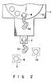
- For example, in an ion implantation unit, as shown in Figure 1, ions generated by an ion generator I disposed in a terminal unit T are deflected by an analysing magnet M and sequentially implanted in a wafer W on a turntable 1a (upright during ion implantation) in a process chamber through an acceleration tube A. Each wafer must be placed on the turntable 1a from the outside to be correctly aligned.
- For this purpose, conventionally, as shown in Fig. 2, wafers W are transferred one by one to an aligning unit OD from a
carrier 3 disposed at a predetermined position outside the process chamber 1 by a transfer robot R1 on the outer air side. An orientation error and a positional error of the center of each wafer are detected by the aligning unit OD, and two correcting steps for correction of the orientation and central position are performed to correct the errors, thus positioning the wafer W. Then, the wafer W in the aligning unit OD is transferred to a load-lock unit 2 by the transfer robot R1. The load-lock unit 2 is evacuated, and the wafer W is transferred to the turntable 1a from the load-lock unit 2 by a transfer robot R2 on the process chamber 1 side. - In such a conventional method, however, when the wafers are transferred into the load-lock unit one by one from the carrier, they must pass through the aligning unit, resulting in an increase in number of wafer handling times. Thus, damage to the wafer tends to occur or particles of dust tend to attach the wafer, leading to a decrease in yield. At the same time, as the number of handling times is increased, the loading time is prolonged, decreasing the processing throughput of the load-lock unit.
- Regarding the aligning unit, a servo mechanism for moving the wafer in X and Y directions is need to correct, e.g., the central position of the wafer. As a result, the aligning unit becomes complicated and costly and requires an additional installation space for the servo mechanism.
- It is an object of the present invention to provide a compact load-lock unit which can increase the throughput and yield.
- It is another object of the present invention to provide a wafer transfer system which can efficiently correct a positional error of a wafer.
- The present invention is characterised by further comprising exhausting means for evacuating the load-lock chamber, and error detecting means, including means for radiating light onto said wafer, for detecting a position error of the center of said wafer and an orientation error of said wafer based on data obtained by the radiating of light on said wafer when said wafer is rotated by said rotating means in the load-lock chamber.
- This invention can be more fully understood from the following detailed description when taken in conjunction with the accompanying drawings, in which:
- Fig. 1 is a view showing an overall arrangement of a conventional ion implantation unit;
- Fig. 2 is a view showing a conventional wafer transfer system of the ion implantation unit;
- Fig. 3 is a longitudinal sectional view showing a load-lock unit according to an embodiment of the present invention;
- Fig. 4 is a view for explaining the positional relationship between a wafer and an optical path;
- Figs. 5 to 8 are sectional views showing various arrangements of a light-receiving section and a light-emitting section;
- Fig. 9 is a view showing a wafer transfer system according to another embodiment of the present invention; and
- Fig. 10 is a sectional view showing a partial arrangement of the load-lock unit shown in Fig. 3.
- The preferred embodiments of the present invention will be described with reference to the accompanying drawings.
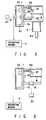
- Fig. 3 is a sectional view showing an arrangement of a load-lock unit according to an embodiment of the present invention. In this embodiment, a bottomed
cylindrical member 4 which is open upward and alid plate 4a constituted by, e.g., a glass plate for closing the open surface of thecylindrical member 4 constitute a load-lock chamber 5. A magnetic seal (not shown) is disposed in a cylindrical base portion 4c vertically extending downward from the central portion of the lower surface of the bottom portion of thecylindrical member 4. A rotatingshaft 4b which rotates about a vertical axis is hermetically inserted in the load-lock chamber 5 at the central position of the bottom portion through the magnetic seal. - A motor (not shown) is coupled to the lower end of the rotating
shaft 4b, and aturntable 4d is provided at the upper end of the rotatingshaft 4b. A chuckunit comprising electrodes 4e for electrostatically chucking a wafer is disposed on the upper surface of theturntable 4b. In this arrangement, the chuck unit and theturntable 4d constitute a holding portion. Air supply paths 6 each having an exhaust path for evacuating the load-lock chamber 5 are provided at, e.g., two portions under thecylindrical member 4. Theair supply paths 6 haveexhaust pipes - A
window 7 constituted by a glass plate is mounted on part of a side surface of thecylindrical member 4, and abox member 7a is mounted on thecylindrical member 4 to cover the outer surface of thewindow 7. A light-emitting section 8a for emitting a laser beam is disposed on the bottom portion of thebox member 7a. Amirror 8b, a cylindrical lens 8c, and a light-receivingsection 8d are housed in thebox member 7a. Themirror 8b reflects the laser beam, which has been emitted upward from the light-emitting section 8a, at a right angle toward the interior of the load-lock chamber 5. The lens 8c shapes the spot of the laser beam into a thin elongated shape. The light-receivingsection 8d receives the laser beam returned from the load-lock chamber 5. - A
mirror 8e which reflects at a right angle a laser beam incident through thewindow 7 in order to form an optical path perpendicular to the path of the wafer and amirror 8f which reflects the laser beam reflected by themirror 8e to the outside of thewindow 7 are arranged in the load-lock chamber 5. The positions of the pair ofmirrors rotating shaft 4b. - The light-emitting section 8a, the
mirror 8b, the lens 8c, and the light-receivingsection 8d constitute a first unit together with thewindow 7 and thebox member 7a. Themirrors lock chamber 5 are mounted on a U-shapedcommon holding member 8g to constitute a second unit and fixed to thewindow 7 through afixing member 8h. - If the respective members are combined to constitute the first and second units as described above, the relative positional relationship among the light-emitting section 8a, the
mirror 8b, and the objective lens 8c and the position of the light-receivingsection 8d of the first unit are preset, and the positions of the pair ofmirrors - The light-receiving
section 8d is connected to an operating means 9 for calculating a positional error amount of the wafer W in the load-lock chamber 5, i.e., the error amount in central position and orientation (rotation angle) of the wafer W on the basis of an electrical signal corresponding to an amount of light received by the light-receivingsection 8d. In Fig. 3, the light-emitting section 8a, the light-receivingsection 8d, and the operating means 9 constitute a positional error detecting means of the wafer. The load-lock unit according to this embodiment has the arrangement described above. - In the above-described embodiment shown in Fig. 3, the light-emitting and light-receiving
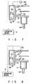
sections 8a and 8d are combined as the first unit and disposed in thebox member 7a. However, they are not limited to this arrangement but can be disposed at various positions. - In an arrangement shown in Fig. 5, a light-emitting section 8a is disposed outside the
box member 7a, and a laser beam emitted from the light-emitting section 8a is incident on a load-lock chamber 5 through atransparent plate 8i. The arrangement shown in Fig. 5 is advantageous in that amirror 8b can be omitted. - In an arrangement shown in Fig. 6, a light-emitting section 8a is disposed below a load-
lock chamber 5, and a laser beam emitted from the light-emitting section 8a is incident on a load-lock chamber 5 through a transparent plate 8j. The arrangement shown in Fig. 6 is advantageous in thatmirrors lock chamber 5. - In an arrangement shown in Fig 7, a light-receiving
section 8d is arranged above a load-lock chamber 5, and a laser beam from the load-lock chamber 5 is incident on the light-receivingsection 8d through atransparent plate 8k. The arrangement shown in Fig. 7 is advantageous in that amirror 8f can be omitted. In the arrangement shown in Fig. 7, the position of a light-emitting section 8a can be any one shown in Fig. 3, 5, or 6. When the light-emitting section 8a is disposed at the position shown in Fig. 6, all the mirrors can be omitted. - In an arrangement shown in Fig. 8, a light-receiving
section 8d is disposed in a load-lock chamber 5. The arrangement shown in Fig. 8 is advantageous in that amirror 8f can be omitted as in Fig. 7. In the arrangement shown in Fig. 8, the position of the light-emitting section 8a can be any one shown in Fig. 3, 5, or 6. - An operation of the load-lock unit described above will be described with reference to Fig. 3.
- A gate (not shown) of the load-
lock chamber 5 on the outer air side is opened, and a non-processed wafer W disposed in an outer air is loaded in the load-lock chamber 5 by a transfer mechanism (not shown) through its intake port, placed on theturntable 4d, and fixed on theturntable 4d by the electrostatic chuck. The gate on the outer air side is closed and the load-lock chamber 5 is evacuated to a predetermined vacuum degree. A motor (not shown) is driven to rotate the wafer W once while the light-emitting section 8a emits a laser beam. If a start point of data detection is near the vertex of the orientation flat, a peak corresponding to the vertex of the orientation flat appears at two ends of the detection data, thus sometimes causing inconvenience in data read access. Hence, the wafer W is normally rotated through about 360° + 5°. - An amount of laser beam received by the light-receiving
section 8d corresponds to the position of the periphery of the wafer W in the laser beam range. Thus, a distance from the center of rotation to the periphery of the wafer W within the laser beam range at each angular position can be obtained by the operating means 9 on the basis of an electrical signal output from the light-receivingsection 8d. The orientation flat ℓ for determining the crystal orientation is formed in the wafer W. Therefore, an error amount of the center of the wafer W from a correct position and an error amount (error amount in rotation angle) of the orientation of the wafer W from a correct position can be simultaneously detected by obtaining the distance described above at each angular position of the wafer W. - The positional error of the center of the wafer need not be that from the correct position but can be a distance from a certain reference point, and the error in rotation angle can be an angle of the orientation flat with respect to a certain reference line.
- Then, the electrostatic chuck is released, a gate (not shown) in the process chamber is opened, and the wafer W is loaded in the process chamber through its outlet port by the transfer mechanism (not shown).
- The positional error of the center of the wafer and the error in rotation angle of the wafer can be detected in this manner in the load-lock unit. In this embodiment, e.g., an aligning mechanism (not shown) may be incorporated in the load-lock unit to correct these errors. Alternatively, alignment may be performed when the wafer is transferred into the process chamber from the load-lock unit as in another embodiment to be described below.
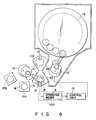
- Fig. 9 shows part of a transfer system for transferring a wafer to a turntable 1a in a process chamber 1 of an ion implantation unit from the outside (atmospheric pressure). In this system, first and second load-lock units 11a and 11b each having an
optical path unit 10 including light-emitting and receiving sections and mirrors as shown in Fig. 3 are disposed adjacent to each other. - A
transfer mechanism 12 comprising, e.g., an articulated robot is provided in the process chamber 1. Acontrol unit 13 for controlling thetransfer mechanism 12 on the basis of an operation result is connected to the output of an operating means 9 connected to theoptical path unit 10.Reference numeral 14 denotes a transfer mechanism on the outer air side; and 15a and 15b, wafer carriers disposed at predetermined positions. - An operation of the system shown in Fig. 9 will be described.
- The non-processed wafers W buffered in the
carrier transfer mechanism 14 through a gate G1 on the outer air side. When one wafer W is transferred, the gate G1 is closed, and the load-lock unit 11a is evacuated. The wafer W is rotated during or after evacuation, as described above, and the positional error of the wafer W is detected by the operating means 9 by a positional error detecting means 100, i.e., on the basis of an electrical signal from theoptical path unit 10. - Subsequently, a gate G2 on the process chamber 1 side is opened and the wafer W in the load-lock unit 11a is transferred to a predetermined position on the turntable 1a by the
transfer mechanism 12. At this time, thecontrol unit 13 supplies a control signal to thetransfer mechanism 12 so that the positional error of the center and the error in rotation angle of the wafer W occurring in the load-lock unit 11a are corrected on the basis of the operation result (positional error amount of the wafer) supplied from the operating means 9 when the wafer W is placed at the predetermined position on the turntable 1a. - Regarding control of the
transfer mechanism 12, the positional error amount may be corrected when thetransfer mechanism 12 is to receive the wafer W in the load-lock unit 11a or 11b or is to place the wafer W on the turntable 1a, or in a process after thetransfer mechanism 12 receives the wafer W and before thetransfer mechanism 12 is to place the wafer W. - Regarding correction of the positional error detected in the load-lock unit, the error in rotation angle of the wafer W may be corrected by the
rotating shaft 4b in the load-lock unit, and only the positional error of the center of the wafer W may be corrected by thetransfer mechanism 12. - Since the system shown in Fig. 9 has two load-lock units, while a wafer W is being loaded from one load-lock unit 11a or 11b in the process chamber 1, alignment (detection of a positional error) of the next wafer W can be performed on the other load-lock unit 11b or 11a. Then, a wait time for alignment can be eliminated to increase the throughput.
- Regarding the gate G1 of each of the load-lock units 11a and 11b, if the wafer inlet port is formed to have a
surface 16 inclined at, e.g., 45° with respect to the vertical axis, and the gate G1 for opening and closing the inlet port is provided with apivotal member 17 which pivots about a horizontal axis P, as shown in Fig. 10, the movement path of the gate G1 will not be widened in the transverse direction, and its movement distance can be minimized, thus minimizing the installation space. In this case, the gate G1 may be linearly moved in the vertical direction in place of being pivoted, or the arrangement described above may be applied to the gate G2 on the side of the process chamber. - Detection of the positional error of the wafer is not limited to the method described in this embodiment, and, e.g., light reflection by the periphery of the wafer may be utilized for this detection.
- The present invention is not limited to wafer transfer between atmospheres having different pressures but can be similarly applied to wafer transfer between atmospheres having different types of gases.
- As has been described above, according to the present invention, since the positional error of the wafer is detected in the load-lock unit, conventional handling of temporarily placing the wafer on the aligning unit can be eliminated. As a result, damage to the wafer and particles of dust attached to the wafer can be decreased, thus increasing the yield. In addition, since the time required for loading can be shortened, the throughput can be increased, and since the aligning unit can be eliminated, the size of the entire system can be reduced. Furthermore, since the positional error is detected on the basis of data obtained by rotation of the wafer, a large-size system such as a TV camera need not be used, thus suppressing an increase in size of the load-lock unit.
- In particular, when the positional error of the wafer detected in the load-lock unit is corrected by the transfer mechanism disposed in the process chamber in, e.g., a vacuum atmosphere, transfer and correction of the positional error can be simultaneously performed, thus further increasing the throughput. In this manner, when the positional error is corrected at the final position of the wafer, e.g., at a position close to the turntable in the process chamber, high-precision alignment can be performed.
Claims (15)
- A load-lock unit which is disposed between first and second atmospheres, for storing a wafer transferred from the first atmosphere, and which is arranged to be blocked off from the first atmosphere, thereafter set in an atmosphere similar to the second atmosphere, and opened so as to communicate with the second atmosphere in order to transfer the wafer to the second atmosphere, said unit comprising:
a load-lock chamber (5);
holding means (4d) disposed in said load-lock chamber, for holding the wafer; and
rotating means (4b) for rotating the wafer held by said holding means;
characterised by further comprising:
exhausting means (6a,6b) for evacuating the load-lock chamber; and
error detecting means, including means for radiating light onto said wafer, for detecting a position error of the center of said wafer and an orientation error of said wafer based on data obtained by the radiating of light on said wafer when said wafer is rotated by said rotating means (4b) in the load-lock chamber (5). - A load-lock unit according to claim 1, characterised in that the error detecting means is arranged to detect said wafer position error and said wafer orientation error based on data obtained by the radiating of light on said wafer when said wafer is rotated by said rotating means (4b) in the load-lock chamber (5) during the evacuation of the load-lock chamber (5) by the exhausting means (6a, 6b).
- A unit according to claim 1, characterised in that said error detecting means comprises an optical unit for generating an electrical signal on the basis of the optical data obtained by radiating light on the wafer which is rotating, and operating means (9), connected to said optical unit, for calculating the electrical signal.
- A unit according to claim 3, characterised in that said optical unit comprises a light-emitting section for emitting a laser beam, and a light-receiving section (8d) for receiving the laser beam emitted from the rotating wafer and converting the laser beam into an electrical signal.
- A unit according to claim 3, characterised in that said light-receiving section (8d) is arranged for receiving the laser beam passing through a peripheral portion of the wafer and detects a light amount thereof.
- A unit according to claim 3, characterised in that said light-receiving section (8d) is arranged for receiving the laser beam reflected by a peripheral portion of the wafer and detects a light amount thereof.
- A unit according to claim 1, characterised in that said rotating means (4b) is arranged to rotate said holding means (4d, 4e).
- A unit according to claim 1, characterised in that said load-lock chamber (5) comprises a wafer inlet port having an open surface (16) which is inclined obliquely downward, and a pivotal member (17) which is pivotal about a horizontal axis for opening and closing the wafer inlet port.
- A transfer system comprising a load-lock unit according to any one of claims 1 to 8, transfer means (12) for transferring the wafer in said load-lock unit (11a, 11b) to a predetermined position in the second atmosphere, and control means (13) for controlling said transfer means (12), said control means (13) being arranged to control said transfer means (12) so that the wafer is disposed at the predetermined position in the second atmosphere after the positional error of the center thereof and the orientation error thereof are corrected on the basis of data from said error detecting means.
- A system according to claim 9, characterised in that said transfer means (12) has a function for correcting the positional error of the center of the wafer and the orientation error of the wafer, and the positional error of the center of the wafer and the orientation error of the wafer are corrected during transfer of the wafer by said transfer means.
- A system according to claim 9, characterised in that means for correcting the positional error of the center of the wafer and the orientation error of the wafer is arranged in said load-lock chamber, and the positional error of the center of the wafer and the orientation error of the wafer are corrected in said load-lock chamber by said error correcting means.
- A system according to claim 9, characterised in that the orientation error of the wafer is corrected by rotation of the wafer by said rotating means.
- A system according to claim 9, characterised in that the orientation error of the wafer is corrected during evacuation of said load-lock chamber.
- A transfer system according to claim 9 comprising a further such load-lock unit, said transfer means (12) being arranged for transferring the wafer in each of said first load-lock unit (11a, 11b) and a second load-lock unit (11a, 11b) to a predetermined position in the second atmosphere.
- A system according to claim 14, characterised in that the positional error of the center of the wafer and the orientation error of the wafer are detected, in use of said transfer system, in said second load-lock unit (11a, 11b) during transfer from said first load-lock (11a, 11b) unit to the second atmosphere.
Applications Claiming Priority (2)
| Application Number | Priority Date | Filing Date | Title |
|---|---|---|---|
| JP87527/91 | 1991-03-26 | ||
| JP8752791AJP2986121B2 (en) | 1991-03-26 | 1991-03-26 | Load lock device and vacuum processing device |
Publications (3)
| Publication Number | Publication Date |
|---|---|
| EP0506045A2 EP0506045A2 (en) | 1992-09-30 |
| EP0506045A3 EP0506045A3 (en) | 1992-11-25 |
| EP0506045B1true EP0506045B1 (en) | 1995-11-29 |
Family
ID=13917472
Family Applications (1)
| Application Number | Title | Priority Date | Filing Date |
|---|---|---|---|
| EP92105208AExpired - LifetimeEP0506045B1 (en) | 1991-03-26 | 1992-03-26 | Load-lock unit and wafer transfer system |
Country Status (5)
| Country | Link |
|---|---|
| US (2) | US5340261A (en) |
| EP (1) | EP0506045B1 (en) |
| JP (1) | JP2986121B2 (en) |
| KR (1) | KR0165556B1 (en) |
| DE (1) | DE69206295T2 (en) |
Cited By (1)
| Publication number | Priority date | Publication date | Assignee | Title |
|---|---|---|---|---|
| US8354656B2 (en) | 2003-01-02 | 2013-01-15 | Loma Linda University Medical Center | Configuration management and retrieval system for proton beam therapy system |
Families Citing this family (326)
| Publication number | Priority date | Publication date | Assignee | Title |
|---|---|---|---|---|
| JP2986121B2 (en)* | 1991-03-26 | 1999-12-06 | 東京エレクトロン株式会社 | Load lock device and vacuum processing device |
| US5812261A (en)* | 1992-07-08 | 1998-09-22 | Active Impulse Systems, Inc. | Method and device for measuring the thickness of opaque and transparent films |
| EP0591706B1 (en)* | 1992-10-06 | 2002-04-24 | Unaxis Balzers Aktiengesellschaft | Chamber for transport of substrates |
| CH686445A5 (en)* | 1992-10-06 | 1996-03-29 | Balzers Hochvakuum | Chamber and chamber combination for a vacuum system and method for passing at least one Werkstueckes. |
| US5516732A (en)* | 1992-12-04 | 1996-05-14 | Sony Corporation | Wafer processing machine vacuum front end method and apparatus |
| US5387067A (en)* | 1993-01-14 | 1995-02-07 | Applied Materials, Inc. | Direct load/unload semiconductor wafer cassette apparatus and transfer system |
| KR100261532B1 (en)* | 1993-03-14 | 2000-07-15 | 야마시타 히데나리 | Multi-chamber system with workpiece conveying device |
| DE4309092C2 (en)* | 1993-03-22 | 1998-11-12 | Joachim Dr Scheerer | Method and device for handling and transporting wafers in ultra-clean rooms |
| US5466117A (en)* | 1993-06-10 | 1995-11-14 | Xilinx, Inc. | Device and method for programming multiple arrays of semiconductor devices |
| US5570987A (en)* | 1993-12-14 | 1996-11-05 | W. L. Gore & Associates, Inc. | Semiconductor wafer transport container |
| US5586585A (en)* | 1995-02-27 | 1996-12-24 | Asyst Technologies, Inc. | Direct loadlock interface |
| JPH09102530A (en)* | 1995-06-07 | 1997-04-15 | Varian Assoc Inc | Direction inspection system of wafer |
| JPH0936198A (en)* | 1995-07-19 | 1997-02-07 | Hitachi Ltd | Vacuum processing apparatus and semiconductor manufacturing line using the same |
| US6672819B1 (en)* | 1995-07-19 | 2004-01-06 | Hitachi, Ltd. | Vacuum processing apparatus and semiconductor manufacturing line using the same |
| US5700046A (en)* | 1995-09-13 | 1997-12-23 | Silicon Valley Group, Inc. | Wafer gripper |
| AU7874098A (en)* | 1996-12-23 | 1998-07-17 | Balzers Aktiengesellschaft | Vacuum treatment equipment |
| US5944476A (en)* | 1997-03-26 | 1999-08-31 | Kensington Laboratories, Inc. | Unitary specimen prealigner and continuously rotatable multiple link robot arm mechanism |
| NL1006461C2 (en)* | 1997-07-03 | 1999-01-05 | Asm Int | Storage assembly for wafers. |
| US6063244A (en)* | 1998-05-21 | 2000-05-16 | International Business Machines Corporation | Dual chamber ion beam sputter deposition system |
| NL1010317C2 (en) | 1998-10-14 | 2000-05-01 | Asm Int | Sorting / storage device for wafers and method for handling them. |
| US6075334A (en)* | 1999-03-15 | 2000-06-13 | Berkeley Process Control, Inc | Automatic calibration system for wafer transfer robot |
| JP2000299367A (en)* | 1999-04-15 | 2000-10-24 | Tokyo Electron Ltd | Processing apparatus and transfer method of article to be processed |
| US6275742B1 (en) | 1999-04-16 | 2001-08-14 | Berkeley Process Control, Inc. | Wafer aligner system |
| GB2349204B (en)* | 1999-04-19 | 2004-03-03 | Applied Materials Inc | A method of detecting the position of a wafer |
| US6244811B1 (en)* | 1999-06-29 | 2001-06-12 | Lam Research Corporation | Atmospheric wafer transfer module with nest for wafer transport robot |
| US6229611B1 (en)* | 1999-09-20 | 2001-05-08 | United Microelectronics Corp. | Method of detecting a transparent quartz wafer in a semiconductor equipment |
| US6364762B1 (en) | 1999-09-30 | 2002-04-02 | Lam Research Corporation | Wafer atmospheric transport module having a controlled mini-environment |
| US6860965B1 (en)* | 2000-06-23 | 2005-03-01 | Novellus Systems, Inc. | High throughput architecture for semiconductor processing |
| US6591161B2 (en)* | 2001-01-31 | 2003-07-08 | Wafermasters, Inc. | Method for determining robot alignment |
| US6556887B2 (en) | 2001-07-12 | 2003-04-29 | Applied Materials, Inc. | Method for determining a position of a robot |
| US6778258B2 (en)* | 2001-10-19 | 2004-08-17 | Asml Holding N.V. | Wafer handling system for use in lithography patterning |
| KR20050044434A (en)* | 2001-11-13 | 2005-05-12 | 에프 에스 아이 인터내셔날,인코포레이티드 | Reduced footprlnt tool for automated processing of microelectronic substrates |
| US6497734B1 (en) | 2002-01-02 | 2002-12-24 | Novellus Systems, Inc. | Apparatus and method for enhanced degassing of semiconductor wafers for increased throughput |
| DE10303460A1 (en)* | 2003-01-29 | 2004-08-19 | Infineon Technologies Ag | Method and device for handling disc-shaped objects |
| US8313277B2 (en) | 2003-11-10 | 2012-11-20 | Brooks Automation, Inc. | Semiconductor manufacturing process modules |
| US8696298B2 (en) | 2003-11-10 | 2014-04-15 | Brooks Automation, Inc. | Semiconductor manufacturing process modules |
| US7458763B2 (en)* | 2003-11-10 | 2008-12-02 | Blueshift Technologies, Inc. | Mid-entry load lock for semiconductor handling system |
| US10086511B2 (en) | 2003-11-10 | 2018-10-02 | Brooks Automation, Inc. | Semiconductor manufacturing systems |
| US20070286710A1 (en)* | 2003-11-10 | 2007-12-13 | Van Der Meulen Peter | Semiconductor manufacturing process modules |
| US20070269297A1 (en) | 2003-11-10 | 2007-11-22 | Meulen Peter V D | Semiconductor wafer handling and transport |
| TWI239933B (en)* | 2004-03-16 | 2005-09-21 | Powerchip Semiconductor Corp | Positioning apparatus and positioning method using the same |
| US20060045668A1 (en)* | 2004-07-19 | 2006-03-02 | Grabowski Al W | System for handling of wafers within a process tool |
| JP4892225B2 (en)* | 2005-10-28 | 2012-03-07 | 株式会社日立ハイテクノロジーズ | Vacuum processing method, vacuum transfer apparatus, and semiconductor processing apparatus |
| US7387484B2 (en)* | 2005-12-21 | 2008-06-17 | Taiwan Semiconductor Manufacturing Co., Ltd. | Wafer positioning systems and methods thereof |
| US20080101912A1 (en)* | 2006-10-26 | 2008-05-01 | Martin Todd W | Deposition analysis for robot motion correction |
| JP2008192840A (en) | 2007-02-05 | 2008-08-21 | Tokyo Electron Ltd | Vacuum processing apparatus, method for vacuum processing and storage medium |
| US20080219807A1 (en) | 2007-03-05 | 2008-09-11 | Van Der Meulen Peter | Semiconductor manufacturing process modules |
| JP5473820B2 (en)* | 2010-07-29 | 2014-04-16 | 株式会社日立ハイテクノロジーズ | Substrate holder and substrate transfer system |
| MY173918A (en) | 2011-02-10 | 2020-02-27 | Hysitron Inc | Nanomechanical testing system |
| US20130023129A1 (en) | 2011-07-20 | 2013-01-24 | Asm America, Inc. | Pressure transmitter for a semiconductor processing environment |
| US10714315B2 (en) | 2012-10-12 | 2020-07-14 | Asm Ip Holdings B.V. | Semiconductor reaction chamber showerhead |
| US8919210B2 (en) | 2012-11-27 | 2014-12-30 | Life Technologies Corporation | Load cell lockouts and related fluid dispensing systems |
| US20160376700A1 (en) | 2013-02-01 | 2016-12-29 | Asm Ip Holding B.V. | System for treatment of deposition reactor |
| US11015245B2 (en) | 2014-03-19 | 2021-05-25 | Asm Ip Holding B.V. | Gas-phase reactor and system having exhaust plenum and components thereof |
| US10941490B2 (en) | 2014-10-07 | 2021-03-09 | Asm Ip Holding B.V. | Multiple temperature range susceptor, assembly, reactor and system including the susceptor, and methods of using the same |
| US10276355B2 (en) | 2015-03-12 | 2019-04-30 | Asm Ip Holding B.V. | Multi-zone reactor, system including the reactor, and method of using the same |
| US10458018B2 (en) | 2015-06-26 | 2019-10-29 | Asm Ip Holding B.V. | Structures including metal carbide material, devices including the structures, and methods of forming same |
| US10211308B2 (en) | 2015-10-21 | 2019-02-19 | Asm Ip Holding B.V. | NbMC layers |
| US10509010B2 (en)* | 2015-11-20 | 2019-12-17 | Shimadzu Corporation | Vacuum processing apparatus and mass spectrometer |
| US11139308B2 (en) | 2015-12-29 | 2021-10-05 | Asm Ip Holding B.V. | Atomic layer deposition of III-V compounds to form V-NAND devices |
| US10529554B2 (en) | 2016-02-19 | 2020-01-07 | Asm Ip Holding B.V. | Method for forming silicon nitride film selectively on sidewalls or flat surfaces of trenches |
| US10343920B2 (en) | 2016-03-18 | 2019-07-09 | Asm Ip Holding B.V. | Aligned carbon nanotubes |
| US10367080B2 (en) | 2016-05-02 | 2019-07-30 | Asm Ip Holding B.V. | Method of forming a germanium oxynitride film |
| US11453943B2 (en) | 2016-05-25 | 2022-09-27 | Asm Ip Holding B.V. | Method for forming carbon-containing silicon/metal oxide or nitride film by ALD using silicon precursor and hydrocarbon precursor |
| US10612137B2 (en) | 2016-07-08 | 2020-04-07 | Asm Ip Holdings B.V. | Organic reactants for atomic layer deposition |
| US9859151B1 (en) | 2016-07-08 | 2018-01-02 | Asm Ip Holding B.V. | Selective film deposition method to form air gaps |
| US9887082B1 (en) | 2016-07-28 | 2018-02-06 | Asm Ip Holding B.V. | Method and apparatus for filling a gap |
| KR102532607B1 (en) | 2016-07-28 | 2023-05-15 | 에이에스엠 아이피 홀딩 비.브이. | Substrate processing apparatus and method of operating the same |
| US9812320B1 (en) | 2016-07-28 | 2017-11-07 | Asm Ip Holding B.V. | Method and apparatus for filling a gap |
| US11532757B2 (en) | 2016-10-27 | 2022-12-20 | Asm Ip Holding B.V. | Deposition of charge trapping layers |
| US10714350B2 (en) | 2016-11-01 | 2020-07-14 | ASM IP Holdings, B.V. | Methods for forming a transition metal niobium nitride film on a substrate by atomic layer deposition and related semiconductor device structures |
| KR102546317B1 (en) | 2016-11-15 | 2023-06-21 | 에이에스엠 아이피 홀딩 비.브이. | Gas supply unit and substrate processing apparatus including the same |
| KR102762543B1 (en) | 2016-12-14 | 2025-02-05 | 에이에스엠 아이피 홀딩 비.브이. | Substrate processing apparatus |
| US11581186B2 (en) | 2016-12-15 | 2023-02-14 | Asm Ip Holding B.V. | Sequential infiltration synthesis apparatus |
| US11447861B2 (en) | 2016-12-15 | 2022-09-20 | Asm Ip Holding B.V. | Sequential infiltration synthesis apparatus and a method of forming a patterned structure |
| KR102700194B1 (en) | 2016-12-19 | 2024-08-28 | 에이에스엠 아이피 홀딩 비.브이. | Substrate processing apparatus |
| US10269558B2 (en) | 2016-12-22 | 2019-04-23 | Asm Ip Holding B.V. | Method of forming a structure on a substrate |
| US11390950B2 (en) | 2017-01-10 | 2022-07-19 | Asm Ip Holding B.V. | Reactor system and method to reduce residue buildup during a film deposition process |
| US10468261B2 (en) | 2017-02-15 | 2019-11-05 | Asm Ip Holding B.V. | Methods for forming a metallic film on a substrate by cyclical deposition and related semiconductor device structures |
| US10529563B2 (en) | 2017-03-29 | 2020-01-07 | Asm Ip Holdings B.V. | Method for forming doped metal oxide films on a substrate by cyclical deposition and related semiconductor device structures |
| US10770286B2 (en) | 2017-05-08 | 2020-09-08 | Asm Ip Holdings B.V. | Methods for selectively forming a silicon nitride film on a substrate and related semiconductor device structures |
| US12040200B2 (en) | 2017-06-20 | 2024-07-16 | Asm Ip Holding B.V. | Semiconductor processing apparatus and methods for calibrating a semiconductor processing apparatus |
| US11306395B2 (en) | 2017-06-28 | 2022-04-19 | Asm Ip Holding B.V. | Methods for depositing a transition metal nitride film on a substrate by atomic layer deposition and related deposition apparatus |
| KR20190009245A (en) | 2017-07-18 | 2019-01-28 | 에이에스엠 아이피 홀딩 비.브이. | Methods for forming a semiconductor device structure and related semiconductor device structures |
| US11018002B2 (en) | 2017-07-19 | 2021-05-25 | Asm Ip Holding B.V. | Method for selectively depositing a Group IV semiconductor and related semiconductor device structures |
| US11374112B2 (en) | 2017-07-19 | 2022-06-28 | Asm Ip Holding B.V. | Method for depositing a group IV semiconductor and related semiconductor device structures |
| US10541333B2 (en) | 2017-07-19 | 2020-01-21 | Asm Ip Holding B.V. | Method for depositing a group IV semiconductor and related semiconductor device structures |
| US10590535B2 (en) | 2017-07-26 | 2020-03-17 | Asm Ip Holdings B.V. | Chemical treatment, deposition and/or infiltration apparatus and method for using the same |
| TWI815813B (en) | 2017-08-04 | 2023-09-21 | 荷蘭商Asm智慧財產控股公司 | Showerhead assembly for distributing a gas within a reaction chamber |
| US10692741B2 (en) | 2017-08-08 | 2020-06-23 | Asm Ip Holdings B.V. | Radiation shield |
| US10770336B2 (en) | 2017-08-08 | 2020-09-08 | Asm Ip Holding B.V. | Substrate lift mechanism and reactor including same |
| US11139191B2 (en) | 2017-08-09 | 2021-10-05 | Asm Ip Holding B.V. | Storage apparatus for storing cassettes for substrates and processing apparatus equipped therewith |
| US11769682B2 (en) | 2017-08-09 | 2023-09-26 | Asm Ip Holding B.V. | Storage apparatus for storing cassettes for substrates and processing apparatus equipped therewith |
| US11830730B2 (en) | 2017-08-29 | 2023-11-28 | Asm Ip Holding B.V. | Layer forming method and apparatus |
| US11056344B2 (en) | 2017-08-30 | 2021-07-06 | Asm Ip Holding B.V. | Layer forming method |
| US11295980B2 (en) | 2017-08-30 | 2022-04-05 | Asm Ip Holding B.V. | Methods for depositing a molybdenum metal film over a dielectric surface of a substrate by a cyclical deposition process and related semiconductor device structures |
| KR102491945B1 (en) | 2017-08-30 | 2023-01-26 | 에이에스엠 아이피 홀딩 비.브이. | Substrate processing apparatus |
| US10658205B2 (en) | 2017-09-28 | 2020-05-19 | Asm Ip Holdings B.V. | Chemical dispensing apparatus and methods for dispensing a chemical to a reaction chamber |
| US10403504B2 (en) | 2017-10-05 | 2019-09-03 | Asm Ip Holding B.V. | Method for selectively depositing a metallic film on a substrate |
| US10923344B2 (en) | 2017-10-30 | 2021-02-16 | Asm Ip Holding B.V. | Methods for forming a semiconductor structure and related semiconductor structures |
| US11022879B2 (en) | 2017-11-24 | 2021-06-01 | Asm Ip Holding B.V. | Method of forming an enhanced unexposed photoresist layer |
| WO2019103613A1 (en) | 2017-11-27 | 2019-05-31 | Asm Ip Holding B.V. | A storage device for storing wafer cassettes for use with a batch furnace |
| CN111344522B (en) | 2017-11-27 | 2022-04-12 | 阿斯莫Ip控股公司 | Including clean mini-environment device |
| US10872771B2 (en) | 2018-01-16 | 2020-12-22 | Asm Ip Holding B. V. | Method for depositing a material film on a substrate within a reaction chamber by a cyclical deposition process and related device structures |
| TWI799494B (en) | 2018-01-19 | 2023-04-21 | 荷蘭商Asm 智慧財產控股公司 | Deposition method |
| KR102695659B1 (en) | 2018-01-19 | 2024-08-14 | 에이에스엠 아이피 홀딩 비.브이. | Method for depositing a gap filling layer by plasma assisted deposition |
| US11081345B2 (en) | 2018-02-06 | 2021-08-03 | Asm Ip Holding B.V. | Method of post-deposition treatment for silicon oxide film |
| WO2019158960A1 (en) | 2018-02-14 | 2019-08-22 | Asm Ip Holding B.V. | A method for depositing a ruthenium-containing film on a substrate by a cyclical deposition process |
| US10896820B2 (en) | 2018-02-14 | 2021-01-19 | Asm Ip Holding B.V. | Method for depositing a ruthenium-containing film on a substrate by a cyclical deposition process |
| US10731249B2 (en) | 2018-02-15 | 2020-08-04 | Asm Ip Holding B.V. | Method of forming a transition metal containing film on a substrate by a cyclical deposition process, a method for supplying a transition metal halide compound to a reaction chamber, and related vapor deposition apparatus |
| KR102636427B1 (en) | 2018-02-20 | 2024-02-13 | 에이에스엠 아이피 홀딩 비.브이. | Substrate processing method and apparatus |
| US10975470B2 (en) | 2018-02-23 | 2021-04-13 | Asm Ip Holding B.V. | Apparatus for detecting or monitoring for a chemical precursor in a high temperature environment |
| US11473195B2 (en) | 2018-03-01 | 2022-10-18 | Asm Ip Holding B.V. | Semiconductor processing apparatus and a method for processing a substrate |
| US11629406B2 (en) | 2018-03-09 | 2023-04-18 | Asm Ip Holding B.V. | Semiconductor processing apparatus comprising one or more pyrometers for measuring a temperature of a substrate during transfer of the substrate |
| US11114283B2 (en) | 2018-03-16 | 2021-09-07 | Asm Ip Holding B.V. | Reactor, system including the reactor, and methods of manufacturing and using same |
| KR102646467B1 (en) | 2018-03-27 | 2024-03-11 | 에이에스엠 아이피 홀딩 비.브이. | Method of forming an electrode on a substrate and a semiconductor device structure including an electrode |
| US11230766B2 (en) | 2018-03-29 | 2022-01-25 | Asm Ip Holding B.V. | Substrate processing apparatus and method |
| US11088002B2 (en) | 2018-03-29 | 2021-08-10 | Asm Ip Holding B.V. | Substrate rack and a substrate processing system and method |
| KR102600229B1 (en) | 2018-04-09 | 2023-11-10 | 에이에스엠 아이피 홀딩 비.브이. | Substrate supporting device, substrate processing apparatus including the same and substrate processing method |
| US12025484B2 (en) | 2018-05-08 | 2024-07-02 | Asm Ip Holding B.V. | Thin film forming method |
| TWI811348B (en) | 2018-05-08 | 2023-08-11 | 荷蘭商Asm 智慧財產控股公司 | Methods for depositing an oxide film on a substrate by a cyclical deposition process and related device structures |
| US12272527B2 (en) | 2018-05-09 | 2025-04-08 | Asm Ip Holding B.V. | Apparatus for use with hydrogen radicals and method of using same |
| KR102596988B1 (en) | 2018-05-28 | 2023-10-31 | 에이에스엠 아이피 홀딩 비.브이. | Method of processing a substrate and a device manufactured by the same |
| TWI840362B (en) | 2018-06-04 | 2024-05-01 | 荷蘭商Asm Ip私人控股有限公司 | Wafer handling chamber with moisture reduction |
| US11718913B2 (en) | 2018-06-04 | 2023-08-08 | Asm Ip Holding B.V. | Gas distribution system and reactor system including same |
| US11286562B2 (en) | 2018-06-08 | 2022-03-29 | Asm Ip Holding B.V. | Gas-phase chemical reactor and method of using same |
| KR102568797B1 (en) | 2018-06-21 | 2023-08-21 | 에이에스엠 아이피 홀딩 비.브이. | Substrate processing system |
| US10797133B2 (en) | 2018-06-21 | 2020-10-06 | Asm Ip Holding B.V. | Method for depositing a phosphorus doped silicon arsenide film and related semiconductor device structures |
| KR102854019B1 (en) | 2018-06-27 | 2025-09-02 | 에이에스엠 아이피 홀딩 비.브이. | Periodic deposition method for forming a metal-containing material and films and structures comprising the metal-containing material |
| TWI873894B (en) | 2018-06-27 | 2025-02-21 | 荷蘭商Asm Ip私人控股有限公司 | Cyclic deposition methods for forming metal-containing material and films and structures including the metal-containing material |
| US10612136B2 (en) | 2018-06-29 | 2020-04-07 | ASM IP Holding, B.V. | Temperature-controlled flange and reactor system including same |
| US10755922B2 (en) | 2018-07-03 | 2020-08-25 | Asm Ip Holding B.V. | Method for depositing silicon-free carbon-containing film as gap-fill layer by pulse plasma-assisted deposition |
| US10388513B1 (en) | 2018-07-03 | 2019-08-20 | Asm Ip Holding B.V. | Method for depositing silicon-free carbon-containing film as gap-fill layer by pulse plasma-assisted deposition |
| US11053591B2 (en) | 2018-08-06 | 2021-07-06 | Asm Ip Holding B.V. | Multi-port gas injection system and reactor system including same |
| US11430674B2 (en) | 2018-08-22 | 2022-08-30 | Asm Ip Holding B.V. | Sensor array, apparatus for dispensing a vapor phase reactant to a reaction chamber and related methods |
| US11024523B2 (en) | 2018-09-11 | 2021-06-01 | Asm Ip Holding B.V. | Substrate processing apparatus and method |
| KR102707956B1 (en) | 2018-09-11 | 2024-09-19 | 에이에스엠 아이피 홀딩 비.브이. | Method for deposition of a thin film |
| US11049751B2 (en) | 2018-09-14 | 2021-06-29 | Asm Ip Holding B.V. | Cassette supply system to store and handle cassettes and processing apparatus equipped therewith |
| CN110970344B (en) | 2018-10-01 | 2024-10-25 | Asmip控股有限公司 | Substrate holding apparatus, system comprising the same and method of using the same |
| US11232963B2 (en) | 2018-10-03 | 2022-01-25 | Asm Ip Holding B.V. | Substrate processing apparatus and method |
| KR102592699B1 (en) | 2018-10-08 | 2023-10-23 | 에이에스엠 아이피 홀딩 비.브이. | Substrate support unit and apparatuses for depositing thin film and processing the substrate including the same |
| KR102546322B1 (en) | 2018-10-19 | 2023-06-21 | 에이에스엠 아이피 홀딩 비.브이. | Substrate processing apparatus and substrate processing method |
| KR102605121B1 (en) | 2018-10-19 | 2023-11-23 | 에이에스엠 아이피 홀딩 비.브이. | Substrate processing apparatus and substrate processing method |
| USD948463S1 (en) | 2018-10-24 | 2022-04-12 | Asm Ip Holding B.V. | Susceptor for semiconductor substrate supporting apparatus |
| US12378665B2 (en) | 2018-10-26 | 2025-08-05 | Asm Ip Holding B.V. | High temperature coatings for a preclean and etch apparatus and related methods |
| US11087997B2 (en) | 2018-10-31 | 2021-08-10 | Asm Ip Holding B.V. | Substrate processing apparatus for processing substrates |
| KR102748291B1 (en) | 2018-11-02 | 2024-12-31 | 에이에스엠 아이피 홀딩 비.브이. | Substrate support unit and substrate processing apparatus including the same |
| US11572620B2 (en) | 2018-11-06 | 2023-02-07 | Asm Ip Holding B.V. | Methods for selectively depositing an amorphous silicon film on a substrate |
| US11031242B2 (en) | 2018-11-07 | 2021-06-08 | Asm Ip Holding B.V. | Methods for depositing a boron doped silicon germanium film |
| US10847366B2 (en) | 2018-11-16 | 2020-11-24 | Asm Ip Holding B.V. | Methods for depositing a transition metal chalcogenide film on a substrate by a cyclical deposition process |
| US10818758B2 (en) | 2018-11-16 | 2020-10-27 | Asm Ip Holding B.V. | Methods for forming a metal silicate film on a substrate in a reaction chamber and related semiconductor device structures |
| US12040199B2 (en) | 2018-11-28 | 2024-07-16 | Asm Ip Holding B.V. | Substrate processing apparatus for processing substrates |
| US11217444B2 (en) | 2018-11-30 | 2022-01-04 | Asm Ip Holding B.V. | Method for forming an ultraviolet radiation responsive metal oxide-containing film |
| KR102636428B1 (en) | 2018-12-04 | 2024-02-13 | 에이에스엠 아이피 홀딩 비.브이. | A method for cleaning a substrate processing apparatus |
| US11158513B2 (en) | 2018-12-13 | 2021-10-26 | Asm Ip Holding B.V. | Methods for forming a rhenium-containing film on a substrate by a cyclical deposition process and related semiconductor device structures |
| TWI874340B (en) | 2018-12-14 | 2025-03-01 | 荷蘭商Asm Ip私人控股有限公司 | Method of forming device structure, structure formed by the method and system for performing the method |
| TWI866480B (en) | 2019-01-17 | 2024-12-11 | 荷蘭商Asm Ip 私人控股有限公司 | Methods of forming a transition metal containing film on a substrate by a cyclical deposition process |
| KR102727227B1 (en) | 2019-01-22 | 2024-11-07 | 에이에스엠 아이피 홀딩 비.브이. | Semiconductor processing device |
| CN111524788B (en) | 2019-02-01 | 2023-11-24 | Asm Ip私人控股有限公司 | Method for forming topologically selective films of silicon oxide |
| TWI873122B (en) | 2019-02-20 | 2025-02-21 | 荷蘭商Asm Ip私人控股有限公司 | Method of filling a recess formed within a surface of a substrate, semiconductor structure formed according to the method, and semiconductor processing apparatus |
| TWI845607B (en) | 2019-02-20 | 2024-06-21 | 荷蘭商Asm Ip私人控股有限公司 | Cyclical deposition method and apparatus for filling a recess formed within a substrate surface |
| KR102626263B1 (en) | 2019-02-20 | 2024-01-16 | 에이에스엠 아이피 홀딩 비.브이. | Cyclical deposition method including treatment step and apparatus for same |
| TWI838458B (en) | 2019-02-20 | 2024-04-11 | 荷蘭商Asm Ip私人控股有限公司 | Apparatus and methods for plug fill deposition in 3-d nand applications |
| TWI842826B (en) | 2019-02-22 | 2024-05-21 | 荷蘭商Asm Ip私人控股有限公司 | Substrate processing apparatus and method for processing substrate |
| KR102858005B1 (en) | 2019-03-08 | 2025-09-09 | 에이에스엠 아이피 홀딩 비.브이. | Method for Selective Deposition of Silicon Nitride Layer and Structure Including Selectively-Deposited Silicon Nitride Layer |
| KR102782593B1 (en) | 2019-03-08 | 2025-03-14 | 에이에스엠 아이피 홀딩 비.브이. | Structure Including SiOC Layer and Method of Forming Same |
| US11742198B2 (en) | 2019-03-08 | 2023-08-29 | Asm Ip Holding B.V. | Structure including SiOCN layer and method of forming same |
| JP2020167398A (en) | 2019-03-28 | 2020-10-08 | エーエスエム・アイピー・ホールディング・ベー・フェー | Door openers and substrate processing equipment provided with door openers |
| KR102809999B1 (en) | 2019-04-01 | 2025-05-19 | 에이에스엠 아이피 홀딩 비.브이. | Method of manufacturing semiconductor device |
| KR20200123380A (en) | 2019-04-19 | 2020-10-29 | 에이에스엠 아이피 홀딩 비.브이. | Layer forming method and apparatus |
| KR20200125453A (en) | 2019-04-24 | 2020-11-04 | 에이에스엠 아이피 홀딩 비.브이. | Gas-phase reactor system and method of using same |
| KR20200130121A (en) | 2019-05-07 | 2020-11-18 | 에이에스엠 아이피 홀딩 비.브이. | Chemical source vessel with dip tube |
| US11289326B2 (en) | 2019-05-07 | 2022-03-29 | Asm Ip Holding B.V. | Method for reforming amorphous carbon polymer film |
| KR20200130652A (en) | 2019-05-10 | 2020-11-19 | 에이에스엠 아이피 홀딩 비.브이. | Method of depositing material onto a surface and structure formed according to the method |
| JP7598201B2 (en) | 2019-05-16 | 2024-12-11 | エーエスエム・アイピー・ホールディング・ベー・フェー | Wafer boat handling apparatus, vertical batch furnace and method |
| JP7612342B2 (en) | 2019-05-16 | 2025-01-14 | エーエスエム・アイピー・ホールディング・ベー・フェー | Wafer boat handling apparatus, vertical batch furnace and method |
| USD975665S1 (en) | 2019-05-17 | 2023-01-17 | Asm Ip Holding B.V. | Susceptor shaft |
| USD947913S1 (en) | 2019-05-17 | 2022-04-05 | Asm Ip Holding B.V. | Susceptor shaft |
| USD935572S1 (en) | 2019-05-24 | 2021-11-09 | Asm Ip Holding B.V. | Gas channel plate |
| USD922229S1 (en) | 2019-06-05 | 2021-06-15 | Asm Ip Holding B.V. | Device for controlling a temperature of a gas supply unit |
| KR20200141002A (en) | 2019-06-06 | 2020-12-17 | 에이에스엠 아이피 홀딩 비.브이. | Method of using a gas-phase reactor system including analyzing exhausted gas |
| KR20200141931A (en) | 2019-06-10 | 2020-12-21 | 에이에스엠 아이피 홀딩 비.브이. | Method for cleaning quartz epitaxial chambers |
| KR20200143254A (en) | 2019-06-11 | 2020-12-23 | 에이에스엠 아이피 홀딩 비.브이. | Method of forming an electronic structure using an reforming gas, system for performing the method, and structure formed using the method |
| USD944946S1 (en) | 2019-06-14 | 2022-03-01 | Asm Ip Holding B.V. | Shower plate |
| USD931978S1 (en) | 2019-06-27 | 2021-09-28 | Asm Ip Holding B.V. | Showerhead vacuum transport |
| KR20210005515A (en) | 2019-07-03 | 2021-01-14 | 에이에스엠 아이피 홀딩 비.브이. | Temperature control assembly for substrate processing apparatus and method of using same |
| JP7499079B2 (en) | 2019-07-09 | 2024-06-13 | エーエスエム・アイピー・ホールディング・ベー・フェー | Plasma device using coaxial waveguide and substrate processing method |
| CN112216646A (en) | 2019-07-10 | 2021-01-12 | Asm Ip私人控股有限公司 | Substrate supporting assembly and substrate processing device comprising same |
| KR20210010307A (en) | 2019-07-16 | 2021-01-27 | 에이에스엠 아이피 홀딩 비.브이. | Substrate processing apparatus |
| KR20210010816A (en) | 2019-07-17 | 2021-01-28 | 에이에스엠 아이피 홀딩 비.브이. | Radical assist ignition plasma system and method |
| KR102860110B1 (en) | 2019-07-17 | 2025-09-16 | 에이에스엠 아이피 홀딩 비.브이. | Methods of forming silicon germanium structures |
| US11643724B2 (en) | 2019-07-18 | 2023-05-09 | Asm Ip Holding B.V. | Method of forming structures using a neutral beam |
| KR20210010817A (en) | 2019-07-19 | 2021-01-28 | 에이에스엠 아이피 홀딩 비.브이. | Method of Forming Topology-Controlled Amorphous Carbon Polymer Film |
| TWI839544B (en) | 2019-07-19 | 2024-04-21 | 荷蘭商Asm Ip私人控股有限公司 | Method of forming topology-controlled amorphous carbon polymer film |
| TWI851767B (en) | 2019-07-29 | 2024-08-11 | 荷蘭商Asm Ip私人控股有限公司 | Methods for selective deposition utilizing n-type dopants and/or alternative dopants to achieve high dopant incorporation |
| CN112309900A (en) | 2019-07-30 | 2021-02-02 | Asm Ip私人控股有限公司 | Substrate processing apparatus |
| CN112309899A (en) | 2019-07-30 | 2021-02-02 | Asm Ip私人控股有限公司 | Substrate processing apparatus |
| US12169361B2 (en) | 2019-07-30 | 2024-12-17 | Asm Ip Holding B.V. | Substrate processing apparatus and method |
| US11587814B2 (en) | 2019-07-31 | 2023-02-21 | Asm Ip Holding B.V. | Vertical batch furnace assembly |
| US11227782B2 (en) | 2019-07-31 | 2022-01-18 | Asm Ip Holding B.V. | Vertical batch furnace assembly |
| US11587815B2 (en) | 2019-07-31 | 2023-02-21 | Asm Ip Holding B.V. | Vertical batch furnace assembly |
| CN112323048B (en) | 2019-08-05 | 2024-02-09 | Asm Ip私人控股有限公司 | Liquid level sensor for chemical source container |
| CN112342526A (en) | 2019-08-09 | 2021-02-09 | Asm Ip私人控股有限公司 | Heater assembly including cooling device and method of using same |
| USD965524S1 (en) | 2019-08-19 | 2022-10-04 | Asm Ip Holding B.V. | Susceptor support |
| USD965044S1 (en) | 2019-08-19 | 2022-09-27 | Asm Ip Holding B.V. | Susceptor shaft |
| JP2021031769A (en) | 2019-08-21 | 2021-03-01 | エーエスエム アイピー ホールディング ビー.ブイ. | Production apparatus of mixed gas of film deposition raw material and film deposition apparatus |
| USD949319S1 (en) | 2019-08-22 | 2022-04-19 | Asm Ip Holding B.V. | Exhaust duct |
| USD979506S1 (en) | 2019-08-22 | 2023-02-28 | Asm Ip Holding B.V. | Insulator |
| USD940837S1 (en) | 2019-08-22 | 2022-01-11 | Asm Ip Holding B.V. | Electrode |
| KR20210024423A (en) | 2019-08-22 | 2021-03-05 | 에이에스엠 아이피 홀딩 비.브이. | Method for forming a structure with a hole |
| USD930782S1 (en) | 2019-08-22 | 2021-09-14 | Asm Ip Holding B.V. | Gas distributor |
| KR20210024420A (en) | 2019-08-23 | 2021-03-05 | 에이에스엠 아이피 홀딩 비.브이. | Method for depositing silicon oxide film having improved quality by peald using bis(diethylamino)silane |
| US11286558B2 (en) | 2019-08-23 | 2022-03-29 | Asm Ip Holding B.V. | Methods for depositing a molybdenum nitride film on a surface of a substrate by a cyclical deposition process and related semiconductor device structures including a molybdenum nitride film |
| KR102806450B1 (en) | 2019-09-04 | 2025-05-12 | 에이에스엠 아이피 홀딩 비.브이. | Methods for selective deposition using a sacrificial capping layer |
| KR102733104B1 (en) | 2019-09-05 | 2024-11-22 | 에이에스엠 아이피 홀딩 비.브이. | Substrate processing apparatus |
| US11562901B2 (en) | 2019-09-25 | 2023-01-24 | Asm Ip Holding B.V. | Substrate processing method |
| CN112593212B (en) | 2019-10-02 | 2023-12-22 | Asm Ip私人控股有限公司 | Method for forming topologically selective silicon oxide film by cyclic plasma enhanced deposition process |
| TW202128273A (en) | 2019-10-08 | 2021-08-01 | 荷蘭商Asm Ip私人控股有限公司 | Gas injection system, reactor system, and method of depositing material on surface of substratewithin reaction chamber |
| KR20210042810A (en) | 2019-10-08 | 2021-04-20 | 에이에스엠 아이피 홀딩 비.브이. | Reactor system including a gas distribution assembly for use with activated species and method of using same |
| TWI846953B (en) | 2019-10-08 | 2024-07-01 | 荷蘭商Asm Ip私人控股有限公司 | Substrate processing device |
| TWI846966B (en) | 2019-10-10 | 2024-07-01 | 荷蘭商Asm Ip私人控股有限公司 | Method of forming a photoresist underlayer and structure including same |
| US12009241B2 (en) | 2019-10-14 | 2024-06-11 | Asm Ip Holding B.V. | Vertical batch furnace assembly with detector to detect cassette |
| TWI834919B (en) | 2019-10-16 | 2024-03-11 | 荷蘭商Asm Ip私人控股有限公司 | Method of topology-selective film formation of silicon oxide |
| US11637014B2 (en) | 2019-10-17 | 2023-04-25 | Asm Ip Holding B.V. | Methods for selective deposition of doped semiconductor material |
| KR102845724B1 (en) | 2019-10-21 | 2025-08-13 | 에이에스엠 아이피 홀딩 비.브이. | Apparatus and methods for selectively etching films |
| KR20210050453A (en) | 2019-10-25 | 2021-05-07 | 에이에스엠 아이피 홀딩 비.브이. | Methods for filling a gap feature on a substrate surface and related semiconductor structures |
| US11646205B2 (en) | 2019-10-29 | 2023-05-09 | Asm Ip Holding B.V. | Methods of selectively forming n-type doped material on a surface, systems for selectively forming n-type doped material, and structures formed using same |
| KR20210054983A (en) | 2019-11-05 | 2021-05-14 | 에이에스엠 아이피 홀딩 비.브이. | Structures with doped semiconductor layers and methods and systems for forming same |
| US11501968B2 (en) | 2019-11-15 | 2022-11-15 | Asm Ip Holding B.V. | Method for providing a semiconductor device with silicon filled gaps |
| KR102861314B1 (en) | 2019-11-20 | 2025-09-17 | 에이에스엠 아이피 홀딩 비.브이. | Method of depositing carbon-containing material on a surface of a substrate, structure formed using the method, and system for forming the structure |
| US11450529B2 (en) | 2019-11-26 | 2022-09-20 | Asm Ip Holding B.V. | Methods for selectively forming a target film on a substrate comprising a first dielectric surface and a second metallic surface |
| CN112951697B (en) | 2019-11-26 | 2025-07-29 | Asmip私人控股有限公司 | Substrate processing apparatus |
| CN112885692B (en) | 2019-11-29 | 2025-08-15 | Asmip私人控股有限公司 | Substrate processing apparatus |
| CN120432376A (en) | 2019-11-29 | 2025-08-05 | Asm Ip私人控股有限公司 | Substrate processing apparatus |
| JP7527928B2 (en) | 2019-12-02 | 2024-08-05 | エーエスエム・アイピー・ホールディング・ベー・フェー | Substrate processing apparatus and substrate processing method |
| KR20210070898A (en) | 2019-12-04 | 2021-06-15 | 에이에스엠 아이피 홀딩 비.브이. | Substrate processing apparatus |
| KR20210078405A (en) | 2019-12-17 | 2021-06-28 | 에이에스엠 아이피 홀딩 비.브이. | Method of forming vanadium nitride layer and structure including the vanadium nitride layer |
| KR20210080214A (en) | 2019-12-19 | 2021-06-30 | 에이에스엠 아이피 홀딩 비.브이. | Methods for filling a gap feature on a substrate and related semiconductor structures |
| JP7730637B2 (en) | 2020-01-06 | 2025-08-28 | エーエスエム・アイピー・ホールディング・ベー・フェー | Gas delivery assembly, components thereof, and reactor system including same |
| JP7636892B2 (en) | 2020-01-06 | 2025-02-27 | エーエスエム・アイピー・ホールディング・ベー・フェー | Channeled Lift Pins |
| US11993847B2 (en) | 2020-01-08 | 2024-05-28 | Asm Ip Holding B.V. | Injector |
| KR20210093163A (en) | 2020-01-16 | 2021-07-27 | 에이에스엠 아이피 홀딩 비.브이. | Method of forming high aspect ratio features |
| KR102675856B1 (en) | 2020-01-20 | 2024-06-17 | 에이에스엠 아이피 홀딩 비.브이. | Method of forming thin film and method of modifying surface of thin film |
| TWI889744B (en) | 2020-01-29 | 2025-07-11 | 荷蘭商Asm Ip私人控股有限公司 | Contaminant trap system, and baffle plate stack |
| TW202513845A (en) | 2020-02-03 | 2025-04-01 | 荷蘭商Asm Ip私人控股有限公司 | Semiconductor structures and methods for forming the same |
| KR20210100010A (en) | 2020-02-04 | 2021-08-13 | 에이에스엠 아이피 홀딩 비.브이. | Method and apparatus for transmittance measurements of large articles |
| US11776846B2 (en) | 2020-02-07 | 2023-10-03 | Asm Ip Holding B.V. | Methods for depositing gap filling fluids and related systems and devices |
| TW202146691A (en) | 2020-02-13 | 2021-12-16 | 荷蘭商Asm Ip私人控股有限公司 | Gas distribution assembly, shower plate assembly, and method of adjusting conductance of gas to reaction chamber |
| KR20210103956A (en) | 2020-02-13 | 2021-08-24 | 에이에스엠 아이피 홀딩 비.브이. | Substrate processing apparatus including light receiving device and calibration method of light receiving device |
| TWI855223B (en) | 2020-02-17 | 2024-09-11 | 荷蘭商Asm Ip私人控股有限公司 | Method for growing phosphorous-doped silicon layer |
| CN113410160A (en) | 2020-02-28 | 2021-09-17 | Asm Ip私人控股有限公司 | System specially used for cleaning parts |
| KR20210113043A (en) | 2020-03-04 | 2021-09-15 | 에이에스엠 아이피 홀딩 비.브이. | Alignment fixture for a reactor system |
| KR20210116240A (en) | 2020-03-11 | 2021-09-27 | 에이에스엠 아이피 홀딩 비.브이. | Substrate handling device with adjustable joints |
| US11876356B2 (en) | 2020-03-11 | 2024-01-16 | Asm Ip Holding B.V. | Lockout tagout assembly and system and method of using same |
| KR102775390B1 (en) | 2020-03-12 | 2025-02-28 | 에이에스엠 아이피 홀딩 비.브이. | Method for Fabricating Layer Structure Having Target Topological Profile |
| US12173404B2 (en) | 2020-03-17 | 2024-12-24 | Asm Ip Holding B.V. | Method of depositing epitaxial material, structure formed using the method, and system for performing the method |
| KR102755229B1 (en) | 2020-04-02 | 2025-01-14 | 에이에스엠 아이피 홀딩 비.브이. | Thin film forming method |
| TWI887376B (en) | 2020-04-03 | 2025-06-21 | 荷蘭商Asm Ip私人控股有限公司 | Method for manufacturing semiconductor device |
| TWI888525B (en) | 2020-04-08 | 2025-07-01 | 荷蘭商Asm Ip私人控股有限公司 | Apparatus and methods for selectively etching silcon oxide films |
| KR20210128343A (en) | 2020-04-15 | 2021-10-26 | 에이에스엠 아이피 홀딩 비.브이. | Method of forming chromium nitride layer and structure including the chromium nitride layer |
| US11821078B2 (en) | 2020-04-15 | 2023-11-21 | Asm Ip Holding B.V. | Method for forming precoat film and method for forming silicon-containing film |
| US11996289B2 (en) | 2020-04-16 | 2024-05-28 | Asm Ip Holding B.V. | Methods of forming structures including silicon germanium and silicon layers, devices formed using the methods, and systems for performing the methods |
| KR20210130646A (en) | 2020-04-21 | 2021-11-01 | 에이에스엠 아이피 홀딩 비.브이. | Method for processing a substrate |
| KR20210132612A (en) | 2020-04-24 | 2021-11-04 | 에이에스엠 아이피 홀딩 비.브이. | Methods and apparatus for stabilizing vanadium compounds |
| CN113555279A (en) | 2020-04-24 | 2021-10-26 | Asm Ip私人控股有限公司 | Methods of forming vanadium nitride-containing layers and structures comprising the same |
| TW202208671A (en) | 2020-04-24 | 2022-03-01 | 荷蘭商Asm Ip私人控股有限公司 | Methods of forming structures including vanadium boride and vanadium phosphide layers |
| KR20210132600A (en) | 2020-04-24 | 2021-11-04 | 에이에스엠 아이피 홀딩 비.브이. | Methods and systems for depositing a layer comprising vanadium, nitrogen, and a further element |
| KR102866804B1 (en) | 2020-04-24 | 2025-09-30 | 에이에스엠 아이피 홀딩 비.브이. | Vertical batch furnace assembly comprising a cooling gas supply |
| KR102783898B1 (en) | 2020-04-29 | 2025-03-18 | 에이에스엠 아이피 홀딩 비.브이. | Solid source precursor vessel |
| KR20210134869A (en) | 2020-05-01 | 2021-11-11 | 에이에스엠 아이피 홀딩 비.브이. | Fast FOUP swapping with a FOUP handler |
| JP7726664B2 (en) | 2020-05-04 | 2025-08-20 | エーエスエム・アイピー・ホールディング・ベー・フェー | Substrate processing system for processing a substrate |
| KR20210137395A (en) | 2020-05-07 | 2021-11-17 | 에이에스엠 아이피 홀딩 비.브이. | Apparatus and methods for performing an in-situ etch of reaction chambers with fluorine-based radicals |
| KR102788543B1 (en) | 2020-05-13 | 2025-03-27 | 에이에스엠 아이피 홀딩 비.브이. | Laser alignment fixture for a reactor system |
| TW202146699A (en) | 2020-05-15 | 2021-12-16 | 荷蘭商Asm Ip私人控股有限公司 | Method of forming a silicon germanium layer, semiconductor structure, semiconductor device, method of forming a deposition layer, and deposition system |
| KR20210143653A (en) | 2020-05-19 | 2021-11-29 | 에이에스엠 아이피 홀딩 비.브이. | Substrate processing apparatus |
| KR102795476B1 (en) | 2020-05-21 | 2025-04-11 | 에이에스엠 아이피 홀딩 비.브이. | Structures including multiple carbon layers and methods of forming and using same |
| KR20210145079A (en) | 2020-05-21 | 2021-12-01 | 에이에스엠 아이피 홀딩 비.브이. | Flange and apparatus for processing substrates |
| TWI873343B (en) | 2020-05-22 | 2025-02-21 | 荷蘭商Asm Ip私人控股有限公司 | Reaction system for forming thin film on substrate |
| KR20210146802A (en) | 2020-05-26 | 2021-12-06 | 에이에스엠 아이피 홀딩 비.브이. | Method for depositing boron and gallium containing silicon germanium layers |
| TWI876048B (en) | 2020-05-29 | 2025-03-11 | 荷蘭商Asm Ip私人控股有限公司 | Substrate processing device |
| TW202212620A (en) | 2020-06-02 | 2022-04-01 | 荷蘭商Asm Ip私人控股有限公司 | Apparatus for processing substrate, method of forming film, and method of controlling apparatus for processing substrate |
| TW202208659A (en) | 2020-06-16 | 2022-03-01 | 荷蘭商Asm Ip私人控股有限公司 | Method for depositing boron containing silicon germanium layers |
| TW202218133A (en) | 2020-06-24 | 2022-05-01 | 荷蘭商Asm Ip私人控股有限公司 | Method for forming a layer provided with silicon |
| TWI873359B (en) | 2020-06-30 | 2025-02-21 | 荷蘭商Asm Ip私人控股有限公司 | Substrate processing method |
| US12431354B2 (en) | 2020-07-01 | 2025-09-30 | Asm Ip Holding B.V. | Silicon nitride and silicon oxide deposition methods using fluorine inhibitor |
| TW202202649A (en) | 2020-07-08 | 2022-01-16 | 荷蘭商Asm Ip私人控股有限公司 | Substrate processing method |
| KR20220010438A (en) | 2020-07-17 | 2022-01-25 | 에이에스엠 아이피 홀딩 비.브이. | Structures and methods for use in photolithography |
| TWI878570B (en) | 2020-07-20 | 2025-04-01 | 荷蘭商Asm Ip私人控股有限公司 | Method and system for depositing molybdenum layers |
| KR20220011092A (en) | 2020-07-20 | 2022-01-27 | 에이에스엠 아이피 홀딩 비.브이. | Method and system for forming structures including transition metal layers |
| US12322591B2 (en) | 2020-07-27 | 2025-06-03 | Asm Ip Holding B.V. | Thin film deposition process |
| KR20220021863A (en) | 2020-08-14 | 2022-02-22 | 에이에스엠 아이피 홀딩 비.브이. | Method for processing a substrate |
| US12040177B2 (en) | 2020-08-18 | 2024-07-16 | Asm Ip Holding B.V. | Methods for forming a laminate film by cyclical plasma-enhanced deposition processes |
| TW202228863A (en) | 2020-08-25 | 2022-08-01 | 荷蘭商Asm Ip私人控股有限公司 | Method for cleaning a substrate, method for selectively depositing, and reaction system |
| US11725280B2 (en) | 2020-08-26 | 2023-08-15 | Asm Ip Holding B.V. | Method for forming metal silicon oxide and metal silicon oxynitride layers |
| TW202229601A (en) | 2020-08-27 | 2022-08-01 | 荷蘭商Asm Ip私人控股有限公司 | Method of forming patterned structures, method of manipulating mechanical property, device structure, and substrate processing system |
| TW202217045A (en) | 2020-09-10 | 2022-05-01 | 荷蘭商Asm Ip私人控股有限公司 | Methods for depositing gap filing fluids and related systems and devices |
| USD990534S1 (en) | 2020-09-11 | 2023-06-27 | Asm Ip Holding B.V. | Weighted lift pin |
| KR20220036866A (en) | 2020-09-16 | 2022-03-23 | 에이에스엠 아이피 홀딩 비.브이. | Silicon oxide deposition method |
| USD1012873S1 (en) | 2020-09-24 | 2024-01-30 | Asm Ip Holding B.V. | Electrode for semiconductor processing apparatus |
| TWI889903B (en) | 2020-09-25 | 2025-07-11 | 荷蘭商Asm Ip私人控股有限公司 | Semiconductor processing method |
| US12009224B2 (en) | 2020-09-29 | 2024-06-11 | Asm Ip Holding B.V. | Apparatus and method for etching metal nitrides |
| KR20220045900A (en) | 2020-10-06 | 2022-04-13 | 에이에스엠 아이피 홀딩 비.브이. | Deposition method and an apparatus for depositing a silicon-containing material |
| CN114293174A (en) | 2020-10-07 | 2022-04-08 | Asm Ip私人控股有限公司 | Gas supply unit and substrate processing apparatus including the same |
| TW202229613A (en) | 2020-10-14 | 2022-08-01 | 荷蘭商Asm Ip私人控股有限公司 | Method of depositing material on stepped structure |
| TW202232565A (en) | 2020-10-15 | 2022-08-16 | 荷蘭商Asm Ip私人控股有限公司 | Method of manufacturing semiconductor device, and substrate treatment apparatus using ether-cat |
| TW202217037A (en) | 2020-10-22 | 2022-05-01 | 荷蘭商Asm Ip私人控股有限公司 | Method of depositing vanadium metal, structure, device and a deposition assembly |
| TW202223136A (en) | 2020-10-28 | 2022-06-16 | 荷蘭商Asm Ip私人控股有限公司 | Method for forming layer on substrate, and semiconductor processing system |
| TW202229620A (en) | 2020-11-12 | 2022-08-01 | 特文特大學 | Deposition system, method for controlling reaction condition, method for depositing |
| TW202229795A (en) | 2020-11-23 | 2022-08-01 | 荷蘭商Asm Ip私人控股有限公司 | A substrate processing apparatus with an injector |
| TW202235649A (en) | 2020-11-24 | 2022-09-16 | 荷蘭商Asm Ip私人控股有限公司 | Methods for filling a gap and related systems and devices |
| TW202235675A (en) | 2020-11-30 | 2022-09-16 | 荷蘭商Asm Ip私人控股有限公司 | Injector, and substrate processing apparatus |
| US12255053B2 (en) | 2020-12-10 | 2025-03-18 | Asm Ip Holding B.V. | Methods and systems for depositing a layer |
| TW202233884A (en) | 2020-12-14 | 2022-09-01 | 荷蘭商Asm Ip私人控股有限公司 | Method of forming structures for threshold voltage control |
| US11946137B2 (en) | 2020-12-16 | 2024-04-02 | Asm Ip Holding B.V. | Runout and wobble measurement fixtures |
| TW202232639A (en) | 2020-12-18 | 2022-08-16 | 荷蘭商Asm Ip私人控股有限公司 | Wafer processing apparatus with a rotatable table |
| TW202242184A (en) | 2020-12-22 | 2022-11-01 | 荷蘭商Asm Ip私人控股有限公司 | Precursor capsule, precursor vessel, vapor deposition assembly, and method of loading solid precursor into precursor vessel |
| TW202231903A (en) | 2020-12-22 | 2022-08-16 | 荷蘭商Asm Ip私人控股有限公司 | Transition metal deposition method, transition metal layer, and deposition assembly for depositing transition metal on substrate |
| TW202226899A (en) | 2020-12-22 | 2022-07-01 | 荷蘭商Asm Ip私人控股有限公司 | Plasma treatment device having matching box |
| US11987884B2 (en) | 2021-04-15 | 2024-05-21 | Jnk Tech | Glass and wafer inspection system and a method of use thereof |
| US11508590B2 (en) | 2021-04-15 | 2022-11-22 | Jnk Tech | Substrate inspection system and method of use thereof |
| USD980814S1 (en) | 2021-05-11 | 2023-03-14 | Asm Ip Holding B.V. | Gas distributor for substrate processing apparatus |
| USD980813S1 (en) | 2021-05-11 | 2023-03-14 | Asm Ip Holding B.V. | Gas flow control plate for substrate processing apparatus |
| USD981973S1 (en) | 2021-05-11 | 2023-03-28 | Asm Ip Holding B.V. | Reactor wall for substrate processing apparatus |
| USD1023959S1 (en) | 2021-05-11 | 2024-04-23 | Asm Ip Holding B.V. | Electrode for substrate processing apparatus |
| USD990441S1 (en) | 2021-09-07 | 2023-06-27 | Asm Ip Holding B.V. | Gas flow control plate |
| USD1060598S1 (en) | 2021-12-03 | 2025-02-04 | Asm Ip Holding B.V. | Split showerhead cover |
Family Cites Families (15)
| Publication number | Priority date | Publication date | Assignee | Title |
|---|---|---|---|---|
| US4457664A (en)* | 1982-03-22 | 1984-07-03 | Ade Corporation | Wafer alignment station |
| US4769523A (en)* | 1985-03-08 | 1988-09-06 | Nippon Kogaku K.K. | Laser processing apparatus |
| US4713551A (en)* | 1986-04-17 | 1987-12-15 | Varian Associates, Inc. | System for measuring the position of a wafer in a cassette |
| US4836733A (en)* | 1986-04-28 | 1989-06-06 | Varian Associates, Inc. | Wafer transfer system |
| US4917556A (en)* | 1986-04-28 | 1990-04-17 | Varian Associates, Inc. | Modular wafer transport and processing system |
| US4752898A (en)* | 1987-01-28 | 1988-06-21 | Tencor Instruments | Edge finding in wafers |
| JPS63187644A (en)* | 1987-01-30 | 1988-08-03 | Nec Corp | Production device for semiconductor |
| US4973217A (en)* | 1987-02-09 | 1990-11-27 | Svg Lithography Systems, Inc. | Wafer handling system |
| US4819167A (en)* | 1987-04-20 | 1989-04-04 | Applied Materials, Inc. | System and method for detecting the center of an integrated circuit wafer |
| US4880348A (en)* | 1987-05-15 | 1989-11-14 | Roboptek, Inc. | Wafer centration device |
| JPH0620097B2 (en)* | 1987-10-20 | 1994-03-16 | 富士通株式会社 | Wafer positioning device |
| JPH025049A (en)* | 1988-06-24 | 1990-01-09 | Fuji Photo Film Co Ltd | Formation of air bleeding path for film unit |
| US5102280A (en)* | 1989-03-07 | 1992-04-07 | Ade Corporation | Robot prealigner |
| JPH0736417B2 (en)* | 1989-10-24 | 1995-04-19 | 株式会社メツクス | Wafer positioning device |
| JP2986121B2 (en)* | 1991-03-26 | 1999-12-06 | 東京エレクトロン株式会社 | Load lock device and vacuum processing device |
- 1991
- 1991-03-26JPJP8752791Apatent/JP2986121B2/ennot_activeExpired - Lifetime
- 1992
- 1992-03-26USUS07/857,832patent/US5340261A/ennot_activeExpired - Lifetime
- 1992-03-26EPEP92105208Apatent/EP0506045B1/ennot_activeExpired - Lifetime
- 1992-03-26DEDE69206295Tpatent/DE69206295T2/ennot_activeExpired - Fee Related
- 1992-03-26KRKR1019920004985Apatent/KR0165556B1/ennot_activeExpired - Fee Related
- 1994
- 1994-08-23USUS08/294,761patent/US5435683A/ennot_activeExpired - Lifetime
Cited By (1)
| Publication number | Priority date | Publication date | Assignee | Title |
|---|---|---|---|---|
| US8354656B2 (en) | 2003-01-02 | 2013-01-15 | Loma Linda University Medical Center | Configuration management and retrieval system for proton beam therapy system |
Also Published As
| Publication number | Publication date |
|---|---|
| EP0506045A3 (en) | 1992-11-25 |
| DE69206295T2 (en) | 1996-05-02 |
| DE69206295D1 (en) | 1996-01-11 |
| KR920018841A (en) | 1992-10-22 |
| US5340261A (en) | 1994-08-23 |
| JPH04298061A (en) | 1992-10-21 |
| US5435683A (en) | 1995-07-25 |
| KR0165556B1 (en) | 1999-02-01 |
| EP0506045A2 (en) | 1992-09-30 |
| JP2986121B2 (en) | 1999-12-06 |
Similar Documents
| Publication | Publication Date | Title |
|---|---|---|
| EP0506045B1 (en) | Load-lock unit and wafer transfer system | |
| EP0506044B1 (en) | Load-lock unit and wafer transfer system | |
| US20100024723A1 (en) | Substrate alignment apparatus and substrate processing apparatus | |
| US20060169208A1 (en) | Substrate processing apparatus and substrate processing method | |
| US6690986B1 (en) | Method of detecting the position of a wafer | |
| JPS61228648A (en) | Semiconductor wafer manufacturing equipment, semiconductor wafer processing equipment and chuck equipment | |
| WO2000075969A1 (en) | Wafer orientation sensor | |
| JP4542893B2 (en) | Substrate loading and unloading station with buffer | |
| KR20040014213A (en) | Reticle handling method, reticle handling apparatus, and exposure apparatus | |
| US20020074635A1 (en) | Exposure apparatus, holder container, device manufacturing method, and device manufacturing unit | |
| US20240105487A1 (en) | Substrate transfer system and image correction method | |
| US8532818B2 (en) | Vacuum chamber | |
| US5780849A (en) | Apparatus for detecting objects to be transferred for use in semiconductor device fabrication apparatus | |
| JP4359365B2 (en) | Substrate processing apparatus and substrate position deviation correction method in substrate processing apparatus | |
| KR20010043979A (en) | Exposure system, method of manufacture thereof, method of wafer transfer, device and method of manufacture device | |
| US20090155452A1 (en) | Thin film deposition apparatus and method thereof | |
| US12322629B2 (en) | Transfer apparatus and transfer method | |
| JP3165947B2 (en) | Vacuum chamber door device | |
| JP2001351958A (en) | Apparatus for manufacturing semiconductor | |
| JP2002164416A (en) | Apparatus for detecting object and processing system using it | |
| JP3160691B2 (en) | Processing equipment | |
| JPH06338558A (en) | Detector and processing device | |
| JPH05294405A (en) | Substrate detector | |
| JP2017191124A (en) | Substrate holding member, conveying device and method thereof, exposure device and method thereof, exposure system, and device manufacturing method | |
| JP2000182561A (en) | Electron beam drawing equipment |
Legal Events
| Date | Code | Title | Description |
|---|---|---|---|
| PUAI | Public reference made under article 153(3) epc to a published international application that has entered the european phase | Free format text:ORIGINAL CODE: 0009012 | |
| 17P | Request for examination filed | Effective date:19920326 | |
| AK | Designated contracting states | Kind code of ref document:A2 Designated state(s):DE FR GB IT | |
| PUAL | Search report despatched | Free format text:ORIGINAL CODE: 0009013 | |
| AK | Designated contracting states | Kind code of ref document:A3 Designated state(s):DE FR GB IT | |
| 17Q | First examination report despatched | Effective date:19940126 | |
| GRAA | (expected) grant | Free format text:ORIGINAL CODE: 0009210 | |
| AK | Designated contracting states | Kind code of ref document:B1 Designated state(s):DE FR GB IT | |
| ITF | It: translation for a ep patent filed | ||
| ET | Fr: translation filed | ||
| REF | Corresponds to: | Ref document number:69206295 Country of ref document:DE Date of ref document:19960111 | |
| PLBE | No opposition filed within time limit | Free format text:ORIGINAL CODE: 0009261 | |
| STAA | Information on the status of an ep patent application or granted ep patent | Free format text:STATUS: NO OPPOSITION FILED WITHIN TIME LIMIT | |
| 26N | No opposition filed | ||
| REG | Reference to a national code | Ref country code:GB Ref legal event code:IF02 | |
| PGFP | Annual fee paid to national office [announced via postgrant information from national office to epo] | Ref country code:GB Payment date:20080326 Year of fee payment:17 | |
| PGFP | Annual fee paid to national office [announced via postgrant information from national office to epo] | Ref country code:DE Payment date:20080407 Year of fee payment:17 Ref country code:FR Payment date:20080311 Year of fee payment:17 | |
| PGFP | Annual fee paid to national office [announced via postgrant information from national office to epo] | Ref country code:IT Payment date:20080328 Year of fee payment:17 | |
| GBPC | Gb: european patent ceased through non-payment of renewal fee | Effective date:20090326 | |
| REG | Reference to a national code | Ref country code:FR Ref legal event code:ST Effective date:20091130 | |
| PG25 | Lapsed in a contracting state [announced via postgrant information from national office to epo] | Ref country code:DE Free format text:LAPSE BECAUSE OF NON-PAYMENT OF DUE FEES Effective date:20091001 | |
| PG25 | Lapsed in a contracting state [announced via postgrant information from national office to epo] | Ref country code:GB Free format text:LAPSE BECAUSE OF NON-PAYMENT OF DUE FEES Effective date:20090326 Ref country code:FR Free format text:LAPSE BECAUSE OF NON-PAYMENT OF DUE FEES Effective date:20091123 | |
| PG25 | Lapsed in a contracting state [announced via postgrant information from national office to epo] | Ref country code:IT Free format text:LAPSE BECAUSE OF NON-PAYMENT OF DUE FEES Effective date:20090326 |