EP0502067B1 - Device for charging electrical energy storage means provided with means for controlling said charging - Google Patents
Device for charging electrical energy storage means provided with means for controlling said chargingDownload PDFInfo
- Publication number
- EP0502067B1 EP0502067B1EP90917674AEP90917674AEP0502067B1EP 0502067 B1EP0502067 B1EP 0502067B1EP 90917674 AEP90917674 AEP 90917674AEP 90917674 AEP90917674 AEP 90917674AEP 0502067 B1EP0502067 B1EP 0502067B1
- Authority
- EP
- European Patent Office
- Prior art keywords
- electrical energy
- storage means
- terminal
- diode
- electrical supply
- Prior art date
- Legal status (The legal status is an assumption and is not a legal conclusion. Google has not performed a legal analysis and makes no representation as to the accuracy of the status listed.)
- Expired - Lifetime
Links
Images


Classifications
- H—ELECTRICITY
- H02—GENERATION; CONVERSION OR DISTRIBUTION OF ELECTRIC POWER
- H02J—CIRCUIT ARRANGEMENTS OR SYSTEMS FOR SUPPLYING OR DISTRIBUTING ELECTRIC POWER; SYSTEMS FOR STORING ELECTRIC ENERGY
- H02J7/00—Circuit arrangements for charging or depolarising batteries or for supplying loads from batteries
- H02J7/02—Circuit arrangements for charging or depolarising batteries or for supplying loads from batteries for charging batteries from AC mains by converters
- H—ELECTRICITY
- H02—GENERATION; CONVERSION OR DISTRIBUTION OF ELECTRIC POWER
- H02J—CIRCUIT ARRANGEMENTS OR SYSTEMS FOR SUPPLYING OR DISTRIBUTING ELECTRIC POWER; SYSTEMS FOR STORING ELECTRIC ENERGY
- H02J2207/00—Indexing scheme relating to details of circuit arrangements for charging or depolarising batteries or for supplying loads from batteries
- H02J2207/20—Charging or discharging characterised by the power electronics converter
Definitions
- the present inventionrelates to a device for charging electrical energy storage means.
- the energy of these dischargescomes from a power pulse generator which comprises means for accumulating electrical energy (themselves comprising a capacitor or a set of capacitors) previously charged under a high electrical voltage.
- These electrical energy storage meansare associated with switching means through which they are discharged into the laser.
- These switching meanscan be associated with one or more magnetic compression stages which make it possible to reduce the time width of the pulses arriving at the laser.
- a power pulse generatoris described in article (1) by JK MITTAL et al. titled “Design and performance of a 20 watt copper laser vapor "and published in J. Phys. E: Sci. Instrum. 21 (1988) pp. 388-392, to which reference will be made.
- the generator described in this articlecomprises (see FIG. 1) a capacitor 2 connected to the positive terminal of a source of direct electric voltage 4 via an inductor 6 and a diode 8.
- the inductor 6is connected, on one side, to the positive terminal of the source 4 and, on the other, to the anode of the diode 8 whose cathode is connected to a terminal of the capacitor 2.
- the laser 10 to be suppliedis mounted between the other terminal of the capacitor 2 and the negative terminal of the source 4.
- Switching meanscomprising a thyratron 12, are mounted between the negative terminal of the source 4 and the connection between the capacitor 2 and the diode 8.
- a capacitor 14, called a "picking" capacitor and a bypass resistor 16are mounted between the electrodes of the laser 10.
- generatorsinclude semiconductor switching devices (thyristors of the GT0 type or transistors of the IGBT type for example).
- Power pulse generatorswhich are known in the state of the art, are subject to instabilities which result in fluctuations in the energy of these pulses, and therefore in fluctuations in the energy of the light pulses generated. by lasers.
- This absorbed energydepends very much on the conditions of discharge in the laser vapor.
- the electrical energy reflected at the level of the laser "head”(vapor, enclosure containing the latter and discharge electrodes in the vapor) takes the form of a variable electrical voltage across the terminals of the energy storage means. electric, voltage which, during the next charge cycle, leads to the fluctuations mentioned above.
- the voltage v for recharging the capacitor 2 after a dischargeis equal to 2 (v1-v0), v1 representing the supply voltage of the capacitor 2 and v0 representing the voltage "initial" (that is to say the voltage after said discharge) at the terminals of the capacitor 2, v0 being due to the electrical energy reflected by the laser. It is the voltage v0 and, consequently, the voltage v which fluctuate.
- generatorscomprising semiconductor switching devices associated with saturable magnetic elements
- these generatorsare moreover subject to instabilities which result in a jitter, that is to say an instability of temporal position of the pulses. supplied to the laser.
- This jitteris inadmissible when connecting several lasers operating as amplifiers.
- the object of the present inventionis to remedy to the instability disadvantages of known generators for supplying metal vapor lasers and in particular copper vapor lasers, by solving the problem of controlling the electrical energy stored in the storage means which these generators comprise .
- the present inventionaims to control the charge of means for accumulating electrical energy (for example a capacitor or a set of capacitors mounted in series or in parallel) by taking account of a residual charge that these means of accumulation are likely to present after discharge.
- means for accumulating electrical energyfor example a capacitor or a set of capacitors mounted in series or in parallel
- Document US-A-4 405 889discloses a device in accordance with the preamble of claim 1.
- This document US-A-4 405 889describes a power supply intended for a repetitive discharge device.
- This power supplyincludes a DC voltage source, a first primary storage capacitor and a second discharge capacitor that is part of the device.
- a first trip circuitis activated and commands the closing of a switch, the first capacitor discharges and the second capacitor charges.
- a second trigger circuitcommands the closing of another switch making it possible to send the discharge current from the first capacitor to an intermediate capacitor which, firstly, charges and must be discharged in a second step.
- FR-A-2,575,010discloses a power supply unit for an electric discharge pulsed laser.
- This power supplyincludes a voltage source continuous, a buffer capacitor mounted in parallel with the source, a set of controlled oscillating charges which is mounted between the source and a reservoir capacitor, a voltage divider mounted in parallel with the reservoir capacitor, a pulse transformer whose l primary winding is connected to the set of oscillating loads and to the secondary winding to which a load is connected, a trip gate connected to the primary winding of the transformer, a reference voltage source, a tilting threshold element whose the comparison input is connected to the midpoint of the voltage divider and another input to the reference source, a pulse trainer whose input is connected to the output of the toggle threshold element and the output, to the control input for the set of oscillating loads.
- the power supplyalso includes a leakage current compensation assembly, the control input of which is connected to the output of the toggle threshold element and which is mounted in parallel with the capacitor-reservoir.
- EP-A-0 226 253discloses an electrical supply circuit for charging an accumulator.
- the present inventionrelates to a device for charging electrical energy storage means according to claim 1.
- diodemeans a means which allows an electric current to flow in only one direction.
- the present inventionalso relates to a charging device according to claim 2.
- the inventionalso relates to a charging device according to claim 3.
- the means capable of absorbing the excess electrical energyare the means of continuous electrical power, the latter comprising means for storing electrical energy, provided for recovering the excess electrical energy.
- the means provided to divert this excess electrical energycan cooperate with these means of continuous electrical supply so that the excess electrical energy is absorbed, as soon as it appears, by the latter.
- the switching meanscan be semiconductor switching means.
- the means for accumulating electrical energycan be intended for the electrical supply of a metal vapor laser.
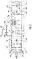
- FIG 2there is shown schematically a device according to the invention, which is intended to impulse charge of electrical energy accumulation means C, for example constituted by a capacitor. This capacitor is charged by a source of continuous electric voltage S.
- the capacitor Cis intended to supply the electrical energy which it has stored at a charge CH.
- the terminals c1 and c2 of the capacitor Care respectively connected to the terminals B1 and B2 of this load CH.
- the capacitor Cis intended for the impulse electrical supply of a metal vapor laser 18 via a switch 20 which is for example a thyratron.
- the switch 20is connected, on the one hand, to the terminal B1 and, on the other, to one of the terminals of the laser 18, the other terminal of which is connected to the terminal B2.
- a “picking” capacitor 22is also mounted between the terminals of the laser 18. The capacitor C, once charged, is discharged impulse into the laser 18 via the switch 20.
- the source Swhich is intended to charge the capacitor C, comprises, by way of indication only and in no way limiting, six diodes D1 to D6, an inductance L1 and a capacitor C1; the cathodes of diodes D2, D4 and D6 are respectively connected to the anodes of diodes D1, D3 and D5, the cathodes of which are connected to a terminal of the inductance L1; the other terminal of L1 is connected to a terminal a1 of the capacitor C1 whose other terminal a2 is connected to the anodes of the diodes D2, D4 and D6; the source S is supplied by the three-phase network 24 and the three conductors of this three-phase network 24 are respectively connected to the anodes of the diodes D1, D3 and D5; we thus have a DC voltage source S whose terminal + corresponds to terminal a1 of capacitor C1 and whose terminal - corresponds to terminal a2 of this capacitor C1.
- the device according to the inventionwhich is schematically represented in FIG. 2, comprises a switch K, which is provided with an on / off control card cm, a transformer T whose primary winding is denoted p and the winding secondary s, a diode d1 and a diode d2.
- the switch Kis an IGBT transistor of the NPN type.
- the cm cardis of the kind used in switching power supplies to control the power transistors of such supplies.
- the cm cardhas two inputs which together constitute a differential input and which are respectively connected to the terminals c1 and c2 of C.
- the cm cardalso has an output which controls the base of the transistor K.
- the collector of transistor Kis connected to the + terminal of the source S.
- the emitter of this transistor Kis connected to one terminal of the primary winding p of the transformer T and the other terminal of this winding p is connected to the anode of diode d1, the cathode of which is connected to terminal c1 of capacitor C.
- the terminal - of the source Sis connected to the terminal c2 of the capacitor C as well as to a terminal of the secondary winding s of the transformer T, the other terminal of this secondary winding s being connected to the anode of the diode d2 whose the cathode is connected to the + terminal of the source S.
- the device schematically represented in FIG. 2comprises magnetic elements among which notably appears the primary winding p of the transformer T, this primary winding p corresponding to the inductance 6 of FIG. 1 and playing the role of this inductance.
- the transfer of the electrical energy from the source 4 to the capacitor 2takes place by means of the magnetic energy stored in the inductor 6.
- this magnetic energyis entirely used to overload the capacitor 2 above the voltage supplied by the source 4.
- This energy transferis unfortunately not controlled and depends on the initial state of charge of the capacitor 2 (c ' i.e. the state of charge following the previous discharge).
- the device shown diagrammatically in FIG. 2makes it possible, on the contrary, to obtain a stable voltage across the terminals of the capacitor C by diverting the excess energy of the magnetic elements which this device comprises and among which is included in particular the primary winding p, towards the source DC voltage S or, in an alternative embodiment which will be described later, to means capable of absorbing this excess energy.
- the control card cmmeasures the voltage across the capacitor C, compares it to a determined threshold and controls the opening of the switch K when this threshold is reached.
- the cm carddetects that the voltage across the capacitors C is below the determined threshold (the latter being greater than the residual voltages likely to exist); the cm card then commands the closing of the switch K; therefore, capacitor C charges and as soon as the voltage across this capacitor reaches the desired voltage (determined threshold), this is detected by the cm card which then controls the opening of the switch K (the excess energy available in the capacitor C1 - which served to charge the capacitor C - then remaining in this capacitor C1).
- diode d1 of the device of FIG. 2is used to prevent the capacitor C from discharging towards the source S.
- the excess energyis not evacuated towards the source S. It is evacuated towards means 26 capable of absorbing this energy and comprising for this purpose a capacitor 28 and an electrical resistance 30.
- the cathode of the diode d2is no longer connected to the + terminal of the source S; this cathode of the diode d2 is connected to a terminal of the capacitor 28, the other terminal of which is connected to the terminal - of the source S; the resistor 30 is mounted between the terminals of the capacitor 28 so that the excess energy, which is absorbed by the means 26, is dissipated by this electrical resistor 30, between two successive discharges of the capacitor C.
- a device according to the inventionwould also be obtained by reversing the polarities of the diodes d1 and d2 and that of the source S (the terminal + then being connected to the terminal c2 and the terminal - being connected to the collector of the transistor K ).
- a GTO thyristorcould be used, the anode, cathode and trigger of which would be connected respectively as the collector, the emitter and the base of the transistor.
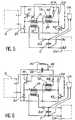
- the device according to the inventionwhich is schematically shown in Figure 3, allows to obtain such galvanic isolation.
- This device of FIG. 3uses an asymmetrical H-bridge.
- the device shown diagrammatically in FIG. 3is also intended to charge a capacitor C whose terminals c1 and c2 are intended to be respectively connected to terminals B1 and B2 of the load CH.
- the device of FIG. 3comprises two switches K1 and K2 as well as a card CM intended to control all-or-nothing simultaneously these switches K1 and K2.
- these two switches K1 and K2are IGBT transistors of the NPN type.
- the CM control cardis of the kind used in switching power supplies to control the power transistors of such supplies.
- the CM cardhas two inputs which together constitute a differential input and which are respectively connected to the terminals c1 and c2 of the capacitor C.
- the CM cardalso has an output which controls both the base of the transistor K1 and the base of the transistor K2 .
- the device shown in FIG. 3also includes four diodes D1, D2, D3 and D4, a transformer T1, the primary winding of which is denoted p1 and the secondary winding of which is denoted s1, and an inductance L.
- a terminal of the secondary winding s1is connected to the anode of the diode D3 whose cathode is connected to the terminal c1 of the capacitor C.
- the other terminal of the secondary winding s1is connected to the terminal c2 of this capacitor C.
- the + terminal of the source Sis connected to the collector of the transistor K1 as well as to the cathode of the diode D2.
- the - terminal of the source Sis connected to the anode of the diode D1, to the anode of the diode D4 and to the emitter of the transistor K2.
- the cathode of the diode D1is connected to the emitter of the transistor K1 as well as to a terminal of the primary winding p1 of the transistor T1.
- the other terminal of this primary windingis connected to the cathode of diode D4 as well as to a terminal of inductance L, the other terminal of which is connected to the anode of diode D2 as well as to the collector of transistor K2.
- the diode D3has the function of preventing the capacitor C from discharging in the direction of the source S.
- inductance Lcorresponds to the inductance 6 of FIG. 1.
- the transformer T1has the function of ensuring the galvanic separation of the load CH from the source S and also allows the adaptation of the voltage of the source S to the voltage of the load CH, by appropriately choosing the report of this transformer T1.
- the primary winding p1 of the transformer T1only shows its leakage inductance.
- the achievement, by the voltage across the capacitor C, of the desired value (determined threshold),is detected by the card CM which then simultaneously controls the opening of the switch K1 and the opening of the switch K2.
- FIG. 4there is shown schematically an alternative embodiment of the device of FIG. 3.
- the excess energyis no longer sent to the source S but to the means 26 already mentioned above.
- the cathode of the diode D2is no longer connected to the + terminal of the source S but is connected to a terminal of the capacitor 28 of the means 26, the other terminal of this capacitor 28 being connected to the terminal - of the source S.
- the electrical resistance 30is still mounted between the terminals of the capacitor 28.
- devices according to the inventionwould also be obtained by reversing, in the devices of FIGS. 3 and 4, the polarities of the diodes D1, D2, D3 and D4 and the polarity of the source S (the + terminal then being connected to the emitter of transistor K2 and the terminal - to the collector of transistor K1).
- FIG 5there is shown schematically another device according to the invention which differs from that which is shown in Figure 3 by the fact that the diode D4 and the inductance L are deleted in this device of Figure 5 and that the latter comprises two new elements, namely an additional transformer T2, whose primary winding is noted p2 and whose secondary winding is noted s2, as well as an additional diode D′4.
- One terminal of the secondary winding s2 of the transformer T2is connected to the - terminal of the source S and the other terminal of this winding s2 is connected to the anode of the diode D′4 whose cathode is connected to the + terminal. source S.
- a terminal of the primary winding p1 of the transformer T1is connected to the emitter of the transistor K1 but the other terminal of this winding p1 is connected to a terminal of the primary winding p2 of the transformer T2, the other terminal of this winding p2 being connected to the anode of diode D2 (this anode of diode D2 being connected, as before, to the collector of transistor K2).
- the transformer T2has the same function as the transformer T in Figure 2.
- the secondary winding s2 of the transformer T2allows the evacuation of the excess energy, present in the magnetic circuit of the transformer T2, towards the source S.
- the diodes D1 and D2are used to restore to the source S the energy stored in the inductors leakage of transformers T1 and T2.
- the device shown in Figure 5has, compared to the device shown in Figure 3, the advantage of allowing less current demand on the components of the device, by a greater transfer of excess energy.
- the device according to the inventionwhich is schematically represented in FIG. 6, differs from that which is represented in FIG. 5 by the fact that the excess energy is no longer sent to the source S but diverted towards the means 26 which have already been mentioned above and which absorb this energy.
- the diode D'4is no longer connected to the + terminal of the source S but is connected to a terminal of the capacitor 28 forming part of the means 26, the other terminal of the capacitor 28 being connected at the - terminal of the source S.
- the electrical resistance 30is mounted between the terminals of the capacitor 28.
- devices according to the inventionwould also be obtained by reversing, in the devices of FIGS. 5 and 6, the polarities of the diodes D1, D2, D'3 and D4 and the polarity of the source S (the terminal + being connected to the emitter of transistor K2 and the terminal - being connected to the collector of transistor K1).
- FIGS. 5 and 6only work if the direction of the coupling of the primary p1 and secondary s1 windings of the transformer T1 and the direction of the coupling of the primary p2 and secondary s2 windings of the transformer T2 are correct. These meanings are conventionally indicated by dots in FIGS. 5 and 6.
- the transformer T1has a low leakage inductance and that the wiring of the elements connected to the secondary winding s1 of the transformer T1 has a low inductance.
- source San exemplary embodiment of which was given above by way of purely indicative and in no way limitative, could be replaced in the devices of FIGS. 2 to 6, by any other source of direct voltage comprising storage means of electrical energy, capable of recovering excess energy.
- a thyristor GTOinstead of an IGBT transistor, one could for example use, as switch K1 or K2, a thyristor GTO, the anode, the cathode and the trigger of this thyristor being respectively connected as the collector, the emitter and the base of the transistor it replaces.
Landscapes
- Engineering & Computer Science (AREA)
- Power Engineering (AREA)
- Dc-Dc Converters (AREA)
- Adhesives Or Adhesive Processes (AREA)
- Addition Polymer Or Copolymer, Post-Treatments, Or Chemical Modifications (AREA)
- Macromonomer-Based Addition Polymer (AREA)
- Sealing Material Composition (AREA)
- Polymerization Catalysts (AREA)
- Generation Of Surge Voltage And Current (AREA)
Abstract
Description
Translated fromFrenchLa présente invention concerne un dispositif de charge de moyens d'accumulation d'énergie électrique.The present invention relates to a device for charging electrical energy storage means.
Elle s'applique notamment à la réalisation d'un générateur de puissance, destiné à l'alimentation électrique impulsionnelle d'un laser à vapeur métallique, un laser à vapeur de cuivre par exemple.It applies in particular to the production of a power generator, intended for the impulse electrical supply of a metal vapor laser, a copper vapor laser for example.
On sait que dans un laser à vapeur métallique et en particulier dans un laser à vapeur de cuivre, on obtient une inversion de population en excitant la vapeur par des décharges électriques de grande puissance instantanée.It is known that in a metallic vapor laser and in particular in a copper vapor laser, a population inversion is obtained by exciting the vapor by electrical discharges of great instantaneous power.
L'énergie de ces décharges provient d'un générateur d'impulsions de puissance qui comporte des moyens d'accumulation d'énergie électrique (comportant eux-mêmes un condensateur ou un ensemble de condensateurs) préalablement chargés sous une tension électrique élevée.The energy of these discharges comes from a power pulse generator which comprises means for accumulating electrical energy (themselves comprising a capacitor or a set of capacitors) previously charged under a high electrical voltage.
Ces moyens d'accumulation d'énergie électrique sont associés à des moyens de commutation par l'intermédiaire desquels ils se déchargent dans le laser.These electrical energy storage means are associated with switching means through which they are discharged into the laser.
Ces moyens de commutation peuvent être associés à un ou des étages de compression magnétique qui permettent de diminuer la largeur temporelle des impulsions parvenant au laser.These switching means can be associated with one or more magnetic compression stages which make it possible to reduce the time width of the pulses arriving at the laser.
Un générateur d'impulsions de puissance est décrit dans l'article (1) de J.K. MITTAL et al. intitulé "Design and performance of a 20 watt copper vapour laser" et publié dans J. Phys. E: Sci. Instrum. 21 (1988) pp. 388-392, auquel on se reportera.A power pulse generator is described in article (1) by JK MITTAL et al. titled "Design and performance of a 20 watt copper laser vapor "and published in J. Phys. E: Sci. Instrum. 21 (1988) pp. 388-392, to which reference will be made.
Le générateur décrit dans cet article comporte (voir figure 1) un condensateur 2 relié à la borne positive d'une source de tension électrique continue 4 par l'intermédiaire d'une inductance 6 et d'une diode 8. L'inductance 6 est reliée, d'un côté, à la borne positive de la source 4 et, de l'autre, à l'anode de la diode 8 dont la cathode est reliée à une borne du condensateur 2.The generator described in this article comprises (see FIG. 1) a
Le laser 10 à alimenter est monté entre l'autre borne du condensateur 2 et la borne négative de la source 4. Des moyens de commutation, comportant un thyratron 12, sont montés entre la borne négative de la source 4 et la connexion entre le condensateur 2 et la diode 8. Un condensateur 14, appelé condensateur de "picking" et une résistance 16 de dérivation sont montées entre les électrodes du laser 10.The
D'autres générateurs connus comportent des dispositifs semiconducteurs de commutation (thyristors de type GT0 ou transistors de type IGBT par exemple).Other known generators include semiconductor switching devices (thyristors of the GT0 type or transistors of the IGBT type for example).
Pour favoriser le commutation, il est également connu d'associer à ces dispositifs semiconducteurs de commutation des éléments magnétiques saturables (inductances saturables).To promote switching, it is also known to combine these semiconductor switching devices with saturable magnetic elements (saturable inductances).
A ce sujet, on pourra se reporter à l'article (2) de H.J. BAKER et al. intitulé "An efficient laser pulser using ferrite magneticswitches" et publié dans J. Phys. E. Sci. Instrum. 21 (1988) pp. 218-224.On this subject, reference may be made to article (2) by H.J. BAKER et al. entitled "An efficient laser pulser using ferrite magneticswitches" and published in J. Phys. E. Sci. Instrum. 21 (1988) pp. 218-224.
Les générateurs d'impulsions de puissance, qui sont connus dans l'état de la technique, sont sujets à des instabilités qui se traduisent par des fluctuations de l'énergie de ces impulsions, et donc des fluctuations de l'énergie des impulsions lumineuses engendrées par les lasers.Power pulse generators, which are known in the state of the art, are subject to instabilities which result in fluctuations in the energy of these pulses, and therefore in fluctuations in the energy of the light pulses generated. by lasers.
Ces fluctuations d'énergie sont en fait dues à la variation de la tension de recharge des moyens d'accumulation d'énergie électrique. Cette variation de tension est elle-même due aux fluctuations de l'énergie électrique absorbée par le laser associé à ces moyens d'accumulation.These energy fluctuations are in fact due to the variation in the recharging voltage of the means for accumulating electrical energy. This variation in voltage is itself due to fluctuations in the electrical energy absorbed by the laser associated with these means of accumulation.
Cette énergie absorbée dépend beaucoup des conditions de décharge dans la vapeur du laser.This absorbed energy depends very much on the conditions of discharge in the laser vapor.
L'énergie électrique réfléchie au niveau de la "tête" du laser (vapeur, enceinte contenant cette dernière et électrodes de décharge dans la vapeur) se présente sous la forme d'une tension électrique variable aux bornes des moyens d'accumulation d'énergie électrique, tension qui, lors du cycle de charge suivant, conduit aux fluctuations mentionnées plus haut.The electrical energy reflected at the level of the laser "head" (vapor, enclosure containing the latter and discharge electrodes in the vapor) takes the form of a variable electrical voltage across the terminals of the energy storage means. electric, voltage which, during the next charge cycle, leads to the fluctuations mentioned above.
Ainsi, dans le générateur décrit dans l'article (1), la tension v de recharge du condensateur 2 après une décharge est égale à 2(v1-v0), v1 représentant la tension d'alimentation du condensateur 2 et v0 représentant la tension "initiale" (c'est-à-dire la tension après ladite décharge) aux bornes du condensateur 2, v0 étant due à l'énergie électrique réfléchie par le laser. C'est la tension v0 et, par conséquent, la tension v qui fluctuent.Thus, in the generator described in article (1), the voltage v for recharging the
Dans le cas des générateurs comportant des dispositifs semi-conducteurs de commutation associés à des éléments magnétiques saturables, ces générateurs sont de plus sujets à des instabilités qui se traduisent par une gigue, c'est-à-dire une instabilité de position temporelle des impulsions électriques fournies au laser. Cette gigue est inadmissible lors de la mise en série de plusieurs lasers fonctionnant en tant qu'amplificateurs.In the case of generators comprising semiconductor switching devices associated with saturable magnetic elements, these generators are moreover subject to instabilities which result in a jitter, that is to say an instability of temporal position of the pulses. supplied to the laser. This jitter is inadmissible when connecting several lasers operating as amplifiers.
La présente invention a pour but de remédier aux inconvénients d'instabilité que présentent les générateurs connus d'alimentation des lasers à vapeur métallique et notamment des lasers à vapeur de cuivre, en résolvant le problème de la maîtrise de l'énergie électrique stockée dans les moyens d'accumulation que comportent ces générateurs.The object of the present invention is to remedy to the instability disadvantages of known generators for supplying metal vapor lasers and in particular copper vapor lasers, by solving the problem of controlling the electrical energy stored in the storage means which these generators comprise .
Plus généralement, la présente invention vise à maîtriser la charge de moyens d'accumulation d'énergie électrique (par exemple un condensateur ou un ensemble de condensateurs montés en série ou en parallèle) en tenant compte d'une charge résiduelle que ces moyens d'accumulation sont susceptibles de présenter, après décharge.More generally, the present invention aims to control the charge of means for accumulating electrical energy (for example a capacitor or a set of capacitors mounted in series or in parallel) by taking account of a residual charge that these means of accumulation are likely to present after discharge.
On connaît par le document US-A-4 405 889 un dispositif conforme au préambule de la revendication 1. Ce document US-A-4 405 889 décrit une alimentation de puissance destinée à un appareil de décharge répétitive. Cette alimentation comprend une source de tension continue, un premier condensateur de stockage primaire et un deuxième condensateur de décharge faisant partie de l'appareil. Lorsque le deuxième condensateur est déchargé, un premier circuit de déclenchement est activé et commande la fermeture d'un interrupteur, le premier condensateur se décharge et le deuxième condensateur se charge. Lorsque la tension entre les bornes de ce deuxième condensateur atteint une valeur prédéterminée, un deuxième circuit de déclenchement commande la fermeture d'un autre interrupteur permettant d'envoyer le courant de décharge du premier condensateur à un condensateur intermédiaire qui, dans un premier temps, se charge et devra être déchargé dans un deuxième temps.Document US-A-4 405 889 discloses a device in accordance with the preamble of claim 1. This document US-A-4 405 889 describes a power supply intended for a repetitive discharge device. This power supply includes a DC voltage source, a first primary storage capacitor and a second discharge capacitor that is part of the device. When the second capacitor is discharged, a first trip circuit is activated and commands the closing of a switch, the first capacitor discharges and the second capacitor charges. When the voltage between the terminals of this second capacitor reaches a predetermined value, a second trigger circuit commands the closing of another switch making it possible to send the discharge current from the first capacitor to an intermediate capacitor which, firstly, charges and must be discharged in a second step.
On connaît par FR-A-2 575 010 un bloc d'alimentation pour laser pulsé à décharge électrique. Ce bloc d'alimentation comprend une source de tension continue, un condensateur tampon monté en parallèle avec la source, un ensemble de charges oscillantes commandées qui est monté entre la source et un condensateur-réservoir, un diviseur de tension monté en parallèle avec le condensateur-réservoir, un transformateur d'impulsions dont l'enroulement primaire est relié à l'ensemble de charges oscillantes et à l'enroulement secondaire auquel est reliée une charge, une porte de déclenchement reliée à l'enroulement primaire du transformateur, une source de tension de référence, un élément à seuil bascule dont l'entrée de comparaison est reliée au point milieu du diviseur de tension et une autre entrée à la source de référence, un formateur d'impulsions dont l'entrée est reliée à la sortie de l'élément à seuil bascule et la sortie, à l'entrée de commande de l'ensemble de charges oscillantes. Le bloc d'alimentation comprend aussi un ensemble de compensation des courants de fuite dont l'entrée de commande est reliée à la sortie de l'élément à seuil bascule et qui est montée en parallèle avec le condensateur-réservoir.FR-A-2,575,010 discloses a power supply unit for an electric discharge pulsed laser. This power supply includes a voltage source continuous, a buffer capacitor mounted in parallel with the source, a set of controlled oscillating charges which is mounted between the source and a reservoir capacitor, a voltage divider mounted in parallel with the reservoir capacitor, a pulse transformer whose l primary winding is connected to the set of oscillating loads and to the secondary winding to which a load is connected, a trip gate connected to the primary winding of the transformer, a reference voltage source, a tilting threshold element whose the comparison input is connected to the midpoint of the voltage divider and another input to the reference source, a pulse trainer whose input is connected to the output of the toggle threshold element and the output, to the control input for the set of oscillating loads. The power supply also includes a leakage current compensation assembly, the control input of which is connected to the output of the toggle threshold element and which is mounted in parallel with the capacitor-reservoir.
On connaît par EP-A-0 226 253 un circuit d'alimentation électrique pour charger un accumulateur.EP-A-0 226 253 discloses an electrical supply circuit for charging an accumulator.
La présente invention a pour objet un dispositif de charge de moyens d'accumulation d'énergie électrique conformément à la revendication 1.The present invention relates to a device for charging electrical energy storage means according to claim 1.
Par "diode", on entend un moyen qui ne laisse passer un courant électrique que dans un seul sens.By "diode" means a means which allows an electric current to flow in only one direction.
La présente invention a également pour objet un dispositif de charge conformément à la revendication 2.The present invention also relates to a charging device according to
L'invention a aussi pour objet un dispositif de charge conforme à la revendication 3.The invention also relates to a charging device according to claim 3.
Dans une réalisation particulière de l'invention, facilitant la mise en oeuvre de celle-ci, les moyens capables d'absorber l'énergie électrique excédentaire sont les moyens d'alimentation électrique continue, ces derniers comportant des moyens de stockage d'énergie électrique, prévus pour récupérer l'énergie électrique excédentaire.In a particular embodiment of the invention, facilitating the implementation thereof, the means capable of absorbing the excess electrical energy are the means of continuous electrical power, the latter comprising means for storing electrical energy, provided for recovering the excess electrical energy.
Dans ce cas, les moyens prévus pour dérouter cette énergie électrique excédentaire peuvent coopérer avec ces moyens d'alimentation électrique continue de façon que l'énergie électrique excédentaire soit absorbée, dès son apparition, par ces derniers.In this case, the means provided to divert this excess electrical energy can cooperate with these means of continuous electrical supply so that the excess electrical energy is absorbed, as soon as it appears, by the latter.
Les moyens de commutation peuvent être des moyens de commutation à semiconducteurs.The switching means can be semiconductor switching means.
Enfin, les moyens d'accumulation d'énergie électrique peuvent être destinés à l'alimentation électrique d'un laser à vapeur métallique.Finally, the means for accumulating electrical energy can be intended for the electrical supply of a metal vapor laser.
La présente invention sera mieux comprise à la lecture de la description suivante, d'exemples de réalisation donnés à titre purement indicatif et nullement limitatif, en référence aux dessins annexés sur lesquels :
- la figure 1, déjà décrite, illustre schématiquement un générateur connu d'impulsions électriques,
- la figure 2 est une vue schématique d'un mode de réalisation particulier du dispositif objet de l'invention,
- la figure 3 est une vue schématique d'un autre mode de réalisation particulier permettant l'isolation galvanique d'une charge, qui est destinée à être alimentée par les moyens d'accumulation que comporte le dispositif de la figure 3, vis-à-vis de la source de tension continue qui alimente ce dispositif,
- la figure 4 illustre schématiquement une variante de réalisation du dispositif de la figure 3,
- la figure 5 est une vue schématique d'un autre mode de réalisation particulier permettant également une telle isolation galvanique, et
- la figure 6 illustre schématiquement une variante de réalisation du dispositif de la figure 5.
- FIG. 1, already described, schematically illustrates a known generator of electrical pulses,
- FIG. 2 is a schematic view of a particular embodiment of the device which is the subject of the invention,
- FIG. 3 is a schematic view of another particular embodiment allowing the galvanic isolation of a load, which is intended to be supplied by the storage means that the device of FIG. 3 comprises, opposite screw of the DC voltage source which supplies this device,
- FIG. 4 schematically illustrates an alternative embodiment of the device of FIG. 3,
- FIG. 5 is a schematic view of another particular embodiment also allowing such galvanic isolation, and
- FIG. 6 schematically illustrates an alternative embodiment of the device of FIG. 5.
Sur la figure 2, on a représenté schématiquement un dispositif conforme à l'invention, qui est destiné à charger de façon impulsionnelle des moyens d'accumulation d'énergie électrique C, par exemple constitués par un condensateur. Ce condensateur est chargé grâce à une source de tension électrique continue S.In Figure 2, there is shown schematically a device according to the invention, which is intended to impulse charge of electrical energy accumulation means C, for example constituted by a capacitor. This capacitor is charged by a source of continuous electric voltage S.
Le condensateur C est destiné à fournir l'énergie électrique qu'il a emmagasinée à une charge CH. Les bornes c1 et c2 du condensateur C sont respectivement reliées aux bornes B1 et B2 de cette charge CH.The capacitor C is intended to supply the electrical energy which it has stored at a charge CH. The terminals c1 and c2 of the capacitor C are respectively connected to the terminals B1 and B2 of this load CH.
A titre purement indicatif et nullement limitatif, le condensateur C est destiné à l'alimentation électrique impulsionnelle d'un laser à vapeur métallique 18 par l'intermédiaire d'un commutateur 20 qui est par exemple un thyratron. Le commutateur 20 est relié, d'un côté, à la borne B1 et, de l'autre, à l'une des bornes du laser 18 dont l'autre borne est reliée à la borne B2. Un condensateur de "picking" 22 est également monté entre les bornes du laser 18. Le condensateur C, une fois chargé, est déchargé de façon impulsionnelle dans le laser 18 par l'intermédiaire du commutateur 20.As a purely indicative and in no way limitative, the capacitor C is intended for the impulse electrical supply of a
La source S, qui est destinée à charger le condensateur C, comprend, à titre purement indicatif et nullement limitatif, six diodes D1 à D6, une inductance L1 et un condensateur C1 ; les cathodes des diodes D2, D4 et D6 sont respectivement reliées aux anodes des diodes D1, D3 et D5 dont les cathodes sont reliées à une borne de l'inductance L1 ; l'autre borne de L1 est reliée à une borne a1 du condensateur C1 dont l'autre borne a2 est reliée aux anodes des diodes D2, D4 et D6 ; la source S est alimentée par le réseau triphasé 24 et les trois conducteurs de ce réseau triphasé 24 sont respectivement reliés aux anodes des diodes D1, D3 et D5 ; on dispose ainsi d'une source de tension continue S dont la borne + correspond à la borne a1 du condensateur C1 et dont la borne - correspond à la borne a2 de ce condensateur C1.The source S, which is intended to charge the capacitor C, comprises, by way of indication only and in no way limiting, six diodes D1 to D6, an inductance L1 and a capacitor C1; the cathodes of diodes D2, D4 and D6 are respectively connected to the anodes of diodes D1, D3 and D5, the cathodes of which are connected to a terminal of the inductance L1; the other terminal of L1 is connected to a terminal a1 of the capacitor C1 whose other terminal a2 is connected to the anodes of the diodes D2, D4 and D6; the source S is supplied by the three-
Le dispositif conforme à l'invention, qui est schématiquement représenté sur la figure 2, comprend un commutateur K, qui est muni d'une carte de commande en tout ou rien cm, un transformateur T dont le bobinage primaire est noté p et le bobinage secondaire s, une diode d1 et une diode d2.The device according to the invention, which is schematically represented in FIG. 2, comprises a switch K, which is provided with an on / off control card cm, a transformer T whose primary winding is denoted p and the winding secondary s, a diode d1 and a diode d2.
A titre purement indicatif et nullement limitatif, le commutateur K est un transistor IGBT de type NPN. La carte cm est du genre de celles qui sont utilisées dans les alimentations électriques à découpage pour commander les transistors de puissance de telles alimentations.By way of indication only and in no way limitative, the switch K is an IGBT transistor of the NPN type. The cm card is of the kind used in switching power supplies to control the power transistors of such supplies.
La carte cm comporte deux entrées qui constituent ensemble une entrée différentielle et qui sont respectivement reliées aux bornes c1 et c2 de C. La carte cm comporte aussi une sortie qui commande la base du transistor K.The cm card has two inputs which together constitute a differential input and which are respectively connected to the terminals c1 and c2 of C. The cm card also has an output which controls the base of the transistor K.
Le collecteur du transistor K est relié à la borne + de la source S. L'émetteur de-ce transistor K est relié à une borne du bobinage primaire p du transformateur T et l'autre borne de ce bobinage p est reliée à l'anode de la diode d1 dont la cathode est reliée à la borne c1 du condensateur C.The collector of transistor K is connected to the + terminal of the source S. The emitter of this transistor K is connected to one terminal of the primary winding p of the transformer T and the other terminal of this winding p is connected to the anode of diode d1, the cathode of which is connected to terminal c1 of capacitor C.
La borne - de la source S est reliée à la borne c2 du condensateur C ainsi qu'à une borne du bobinage secondaire s du transformateur T, l'autre borne de ce bobinage secondaire s étant reliée à l'anode de la diode d2 dont la cathode est reliée à la borne + de la source S.The terminal - of the source S is connected to the terminal c2 of the capacitor C as well as to a terminal of the secondary winding s of the transformer T, the other terminal of this secondary winding s being connected to the anode of the diode d2 whose the cathode is connected to the + terminal of the source S.
On notera que le dispositif schématiquement représenté sur la figure 2 comprend des éléments magnétiques parmi lesquels figure notamment le bobinage primaire p du transformateur T, ce bobinage primaire p correspondant à l'inductance 6 de la figure 1 et jouant le rôle de cette inductance. Dans le dispositif représenté sur cette figure 1, le transfert de l'énergie électrique de la source 4 vers le condensateur 2 se fait par l'intermédiaire de l'énergie magnétique emmagasinée dans l'inductance 6.It will be noted that the device schematically represented in FIG. 2 comprises magnetic elements among which notably appears the primary winding p of the transformer T, this primary winding p corresponding to the inductance 6 of FIG. 1 and playing the role of this inductance. In the device represented in this FIG. 1, the transfer of the electrical energy from the source 4 to the
En général, cette énergie magnétique est entièrement utilisée pour surcharger le condensateur 2 au-dessus de la tension fournie par la source 4. Ce transfert énergétique n'est malheureusement pas maitrisé et dépend de l'état de charge initial du condensateur 2 (c'est-à-dire l'état de charge suivant la précédente décharge).In general, this magnetic energy is entirely used to overload the
Le dispositif schématiquement représenté sur la figure 2 permet, au contraire, d'obtenir une tension stable aux bornes du condensateur C en déroutant l'énergie excédentaire des éléments magnétiques que comporte ce dispositif et parmi lesquels figure notamment le bobinage primaire p, vers la source de tension continue S ou, dans une variante de réalisation qui sera décrite par la suite, vers des moyens capables d'absorber cette énergie excédentaire.The device shown diagrammatically in FIG. 2 makes it possible, on the contrary, to obtain a stable voltage across the terminals of the capacitor C by diverting the excess energy of the magnetic elements which this device comprises and among which is included in particular the primary winding p, towards the source DC voltage S or, in an alternative embodiment which will be described later, to means capable of absorbing this excess energy.
La carte de commande cm mesure la tension aux bornes du condensateur C, compare celle-ci à un seuil déterminé et commande l'ouverture du commutateur K lorsque ce seuil est atteint.The control card cm measures the voltage across the capacitor C, compares it to a determined threshold and controls the opening of the switch K when this threshold is reached.
Plus précisément, à la fin du cycle de charge-décharge précédent, il existe aux bornes du condensateurs C une tension résiduelle et la carte cm détecte que la tension aux bornes du condensateur C est inférieure au seuil déterminé (ce dernier étant supérieur aux tensions résiduelles susceptibles d'exister) ; la carte cm commande alors la fermeture du commutateur K ; par conséquent, le condensateur C se charge et dès que la tension aux bornes de ce condensateur atteint la tension souhaitée (seuil déterminé), ceci est détecté par la carte cm qui commande alors l'ouverture du commutateur K (l'énergie excédentaire disponible dans le condensateur C1 - qui a servi à charger le condensateur C - demeurant alors dans ce condensateur C1).More precisely, at the end of the previous charge-discharge cycle, there is a residual voltage across the capacitors C and the cm card detects that the voltage across the capacitors C is below the determined threshold (the latter being greater than the residual voltages likely to exist); the cm card then commands the closing of the switch K; therefore, capacitor C charges and as soon as the voltage across this capacitor reaches the desired voltage (determined threshold), this is detected by the cm card which then controls the opening of the switch K (the excess energy available in the capacitor C1 - which served to charge the capacitor C - then remaining in this capacitor C1).
Cependant, il existe, lors de l'ouverture du commutateur K, de l'énergie dans le transformateur T et cette énergie ne doit pas aller vers le condensateur C. Cette énergie excédentaire ne peut être évacuée à travers le bobinage primaire p du transformateur T puisque le commutateur K est ouvert. Elle est donc évacuée à travers le bobinage secondaire s du transformateur T et la diode passante d2 et retourne ainsi à la source S où elle est récupérée par stockage dans le condensateur C1.However, when the switch K opens, there is energy in the transformer T and this energy must not go to the capacitor C. This excess energy cannot be evacuated through the primary winding p of the transformer T since switch K is open. It is therefore discharged through the secondary winding s of the transformer T and the pass-through diode d2 and thus returns to the source S where it is recovered by storage in the capacitor C1.
L'évacuation de cette énergie excédentaire (de type magnétique) n'est possible que si le couplage des bobinages primaire p et secondaire s dans le transformateur T est dans le bon sens. Ce sens est indiqué de façon classique, par des points sur la figure 2 à laquelle on se reportera.The removal of this excess energy (of magnetic type) is only possible if the coupling of the primary p and secondary windings s in the transformer T is in the right direction. This direction is conventionally indicated by dots in Figure 2 to which reference will be made.
On notera que cette énergie excédentaire est absorbée par la source S dès qu'elle apparaît dans le dispositif. Il en est c'ailleurs de même pour les dispositifs des figures 3 et 5 où les énergies excédentaires qui apparaissent dans ces dispositifs sont absorbés, dès leur apparition, par la source S.Note that this excess energy is absorbed by the source S as soon as it appears in the device. It is the same for the devices of FIGS. 3 and 5 where the excess energies which appear in these devices are absorbed, from their appearance, by the source S.
On précise que la diode d1 du dispositif de la figure 2 sert à empêcher que le condensateur C se décharge vers la source S.It is specified that the diode d1 of the device of FIG. 2 is used to prevent the capacitor C from discharging towards the source S.
Dans une variante de réalisation, qui est schématiquement représentée en traits mixtes sur la figure 2, l'énergie excédentaire n'est pas évacuée vers la source S. Elle est évacuée vers des moyens 26 capables d'absorber cette énergie et comportant à cet effet un condensateur 28 et une résistance électrique 30.In an alternative embodiment, which is schematically represented in dashed lines in FIG. 2, the excess energy is not evacuated towards the source S. It is evacuated towards
Le dispositif est alors modifié de la façon suivante : la cathode de la diode d2 n'est plus reliée à la borne + de la source S ; cette cathode de la diode d2 est reliée à une borne du condensateur 28 dont l'autre borne est reliée à la borne - de la source S ; la résistance 30 est montée entre les bornes du condensateur 28 de sorte que l'énergie excédentaire, qui est absorbée par les moyens 26, est dissipée par cette résistance électrique 30, entre deux décharges successives du condensateur C.The device is then modified as follows: the cathode of the diode d2 is no longer connected to the + terminal of the source S; this cathode of the diode d2 is connected to a terminal of the
Bien entendu, on obtiendrait encore un dispositif conforme à l'invention en inversant les polarités des diodes d1 et d2 et celle de la source S (la borne + étant alors connectée à la borne c2 et la borne - étant connectée au collecteur du transistor K).Of course, a device according to the invention would also be obtained by reversing the polarities of the diodes d1 and d2 and that of the source S (the terminal + then being connected to the terminal c2 and the terminal - being connected to the collector of the transistor K ).
On notera que le dispositif représenté sur la figure 2 et sa variante, qui est représentée en traits mixtes sur cette figure 2, ne permettent pas l'isolation galvanique de la charge CH vis-à-vis de la source S.Note that the device shown in Figure 2 and its variant, which is shown in phantom in this figure 2, do not allow the galvanic isolation of the load CH from the source S.
En tant que commutateur K, on pourrait par exemple utiliser, au lieu d'un transistor IGBT, un thyristor GTO dont l'anode, la cathode et la gâchette seraient respectivement connectées comme le collecteur, l'émetteur et la base du transistor.As a switch K, for example, instead of an IGBT transistor, a GTO thyristor could be used, the anode, cathode and trigger of which would be connected respectively as the collector, the emitter and the base of the transistor.
Le dispositif conforme à l'invention, qui est schématiquement représenté sur la figure 3, permet d'obtenir une telle isolation galvanique. Ce dispositif de la figure 3 utilise un pont en H dissymétrique.The device according to the invention, which is schematically shown in Figure 3, allows to obtain such galvanic isolation. This device of FIG. 3 uses an asymmetrical H-bridge.
Le dispositif schématiquement représenté sur la figure 3 est encore destiné à charger un condensateur C dont les bornes c1 et c2 sont destinées à être respectivement reliées aux bornes B1 et B2 de la charge CH.The device shown diagrammatically in FIG. 3 is also intended to charge a capacitor C whose terminals c1 and c2 are intended to be respectively connected to terminals B1 and B2 of the load CH.
Le dispositif de la figure 3 comprend deux commutateurs K1 et K2 ainsi qu'une carte CM destinée à commander simultanément en tout ou rien ces commutateurs K1 et K2.The device of FIG. 3 comprises two switches K1 and K2 as well as a card CM intended to control all-or-nothing simultaneously these switches K1 and K2.
A titre purement indicatif et nullement limitatif, ces deux commutateurs K1 et K2 sont des transistors IGBT de type NPN. La carte de commande CM est du genre de celles qui sont utilisées dans les alimentations électriques à découpage pour commander les transistors de puissance de telles alimentations.As a purely indicative and in no way limitative, these two switches K1 and K2 are IGBT transistors of the NPN type. The CM control card is of the kind used in switching power supplies to control the power transistors of such supplies.
La carte CM comporte deux entrées et qui constituent ensemble une entrée différentielle et qui sont respectivement reliées aux bornes c1 et c2 du condensateur C. La carte CM comporte également une sortie qui commande à la fois la base du transistor K1 et la base du transistor K2.The CM card has two inputs which together constitute a differential input and which are respectively connected to the terminals c1 and c2 of the capacitor C. The CM card also has an output which controls both the base of the transistor K1 and the base of the transistor K2 .
Le dispositif représenté sur la figure 3 comprend également quatre diodes D1, D2, D3 et D4, un transformateur T1, dont le bobinage primaire est noté p1 et dont le bobinage secondaire est noté s1, et une inductance L.The device shown in FIG. 3 also includes four diodes D1, D2, D3 and D4, a transformer T1, the primary winding of which is denoted p1 and the secondary winding of which is denoted s1, and an inductance L.
Une borne du bobinage secondaire s1 est reliée à l'anode de la diode D3 dont la cathode est reliée à la borne c1 du condensateur C. L'autre borne du bobinage secondaire s1 est reliée à la borne c2 de ce condensateur C.A terminal of the secondary winding s1 is connected to the anode of the diode D3 whose cathode is connected to the terminal c1 of the capacitor C. The other terminal of the secondary winding s1 is connected to the terminal c2 of this capacitor C.
La borne + de la source S est reliée au collecteur du transistor K1 ainsi qu'à la cathode de la diode D2. La borne - de la source S est reliée à l'anode de la diode D1, à l'anode de la diode D4 et à l'émetteur du transistor K2. La cathode de la diode D1 est reliée à l'émetteur du transistor K1 ainsi qu'à une borne du bobinage primaire p1 du transistor T1. L'autre borne de ce bobinage primaire est reliée à la cathode de la diode D4 ainsi qu'à une borne de l'inductance L dont l'autre borne est reliée à l'anode de la diode D2 ainsi qu'au collecteur du transistor K2.The + terminal of the source S is connected to the collector of the transistor K1 as well as to the cathode of the diode D2. The - terminal of the source S is connected to the anode of the diode D1, to the anode of the diode D4 and to the emitter of the transistor K2. The cathode of the diode D1 is connected to the emitter of the transistor K1 as well as to a terminal of the primary winding p1 of the transistor T1. The other terminal of this primary winding is connected to the cathode of diode D4 as well as to a terminal of inductance L, the other terminal of which is connected to the anode of diode D2 as well as to the collector of transistor K2.
On explique ci-après le fonctionnement du dispositif représenté sur la figure 3.The operation of the device shown in FIG. 3 is explained below.
Lorsque le condensateur C a fourni, au cours d'une décharge précédente, l'énergie qu'il contenait à la charge CH et ne présente plus à ses bornes qu'une tension résiduelle, ceci est détecté par la carte CM qui commande alors la fermeture simultanée des commutateurs K1 et K2. Ceci permet à la source S de recharger le condensateur C par l'intermédiaire du transformateur T1.When the capacitor C has supplied, during a previous discharge, the energy which it contained to the charge CH and only has a residual voltage at its terminals, this is detected by the card CM which then controls the simultaneous closing of switches K1 and K2. This allows the source S to recharge the capacitor C via the transformer T1.
La diode D3 a pour fonction d'empêcher le condensateur C de se décharger en direction de la source S.The diode D3 has the function of preventing the capacitor C from discharging in the direction of the source S.
On notera que l'inductance L correspond à l'inductance 6 de la figure 1.It will be noted that the inductance L corresponds to the inductance 6 of FIG. 1.
Le transformateur T1 a pour fonction d'assurer la séparation galvanique de la charge CH vis-à-vis de la source S et permet également l'adaptation de la tension de la source S à la tension de la charge CH, en choisissant convenablement le rapport de ce transformateur T1.The transformer T1 has the function of ensuring the galvanic separation of the load CH from the source S and also allows the adaptation of the voltage of the source S to the voltage of the load CH, by appropriately choosing the report of this transformer T1.
On notera que, dans le dispositif de la figure 3, le bobinage primaire p1 du transformateur T1 ne fait apparaître que son inductance de fuite.It will be noted that, in the device of FIG. 3, the primary winding p1 of the transformer T1 only shows its leakage inductance.
L'atteinte, par la tension aux bornes du condensateur C, de la valeur souhaitée (seuil déterminé), est détectée par la carte CM qui commande alors simultanément l'ouverture du commutateur K1 et l'ouverture du commutateur K2.The achievement, by the voltage across the capacitor C, of the desired value (determined threshold), is detected by the card CM which then simultaneously controls the opening of the switch K1 and the opening of the switch K2.
Alors, il se produit une circulation de courant électrique, dû à l'énergie excédentaire dans l'inductance L, de la borne - à la borne + de la source S en passant par D4, L et D2 ; de même il se produit une circulation de courant électrique, dû à l'énergie excédentaire dans l'inductance de fuite du transformateur T1, de la borne - à la borne + de la source S en passant par D1, p1, L et D4 ; de ce fait, ces énergies excédentaires sont envoyées à la source S où elle sont absorbées grâce au condensateur C1.So there is an electrical current flow, due to the excess energy in inductance L, from terminal - to terminal + of source S via D4, L and D2; in the same way there is a circulation of electric current, due to the excess energy in the leakage inductance of the transformer T1, from the terminal - to the terminal + of the source S passing through D1, p1, L and D4; therefore, these excess energies are sent to the source S where they are absorbed by the capacitor C1.
Sur la figure 4, on a représenté schématiquement une variante de réalisation du dispositif de la figure 3.In FIG. 4, there is shown schematically an alternative embodiment of the device of FIG. 3.
Dans le dispositif de la figure 4, l'énergie excédentaire n'est plus envoyée à la source S mais aux moyens 26 déjà mentionnés plus haut. A cet effet, dans le dispositif de la figure 4, la cathode de la diode D2 n'est plus reliée à la borne + de la source S mais est reliée à une borne du condensateur 28 des moyens 26, l'autre borne de ce condensateur 28 étant reliée à la borne - de la source S. La résistance électrique 30 est encore montée entre les bornes du condensateur 28.In the device of FIG. 4, the excess energy is no longer sent to the source S but to the
Bien entendu, on obtiendrait encore des dispositifs conformes à l'invention en inversant, dans les dispositifs des figures 3 et 4, les polarités des diodes D1, D2, D3 et D4 et la polarité de la source S (la borne + se trouvant alors reliée à l'émetteur du transistor K2 et la borne - au collecteur du transistor K1).Of course, devices according to the invention would also be obtained by reversing, in the devices of FIGS. 3 and 4, the polarities of the diodes D1, D2, D3 and D4 and the polarity of the source S (the + terminal then being connected to the emitter of transistor K2 and the terminal - to the collector of transistor K1).
On notera que, pour que les dispositifs des figures 3 et 4 fonctionnent, le couplage des bobinages primaire p1 et secondaire s1 du transformateur T1 doit être dans le bon sens. Ce sens est indiqué, de façon classique, par des points sur les figures 3 et 4.It will be noted that, for the devices of FIGS. 3 and 4 to work, the coupling of the primary p1 and secondary s1 windings of the transformer T1 must be in the right direction. This direction is conventionally indicated by dots in FIGS. 3 and 4.
Sur la figure 5, on a représenté schématiquement un autre dispositif conforme à l'invention qui diffère de celui qui est représenté sur la figure 3 par le fait que la diode D4 et l'inductance L sont supprimées dans ce dispositif de la figure 5 et que ce dernier comprend deux nouveaux éléments, à savoir un transformateur supplémentaire T2, dont le bobinage primaire est noté p2 et dont le bobinage secondaire est noté s2, ainsi qu'une diode supplémentaire D′4.In Figure 5, there is shown schematically another device according to the invention which differs from that which is shown in Figure 3 by the fact that the diode D4 and the inductance L are deleted in this device of Figure 5 and that the latter comprises two new elements, namely an additional transformer T2, whose primary winding is noted p2 and whose secondary winding is noted s2, as well as an additional diode D′4.
Une borne du bobinage secondaire s2 du transformateur T2 est reliée à la borne - de la source S et l'autre borne de ce bobinage s2 est reliée à l'anode de la diode D′4 dont la cathode est reliée à la borne + de la source S.One terminal of the secondary winding s2 of the transformer T2 is connected to the - terminal of the source S and the other terminal of this winding s2 is connected to the anode of the diode D′4 whose cathode is connected to the + terminal. source S.
Comme précédemment, une borne du bobinage primaire p1 du transformateur T1 est reliée à l'émetteur du transistor K1 mais l'autre borne de ce bobinage p1 est reliée à une borne du bobinage primaire p2 du transformateur T2, l'autre borne de ce bobinage p2 étant reliée à l'anode de la diode D2 (cette anode de la diode D2 étant reliée, comme précédemment, au collecteur du transistor K2).As before, a terminal of the primary winding p1 of the transformer T1 is connected to the emitter of the transistor K1 but the other terminal of this winding p1 is connected to a terminal of the primary winding p2 of the transformer T2, the other terminal of this winding p2 being connected to the anode of diode D2 (this anode of diode D2 being connected, as before, to the collector of transistor K2).
Le transformateur T2 a la même fonction que le transformateur T de la figure 2.The transformer T2 has the same function as the transformer T in Figure 2.
Le bobinage secondaire s2 du tranformateur T2 permet l'évacuation de l'énergie excédentaire, présente dans le circuit magnétique du transformateur T2, vers la source S. Les diodes D1 et D2 servent à restituer à la source S l'énergie emmagasinée dans les inductances de fuite des transformateurs T1 et T2.The secondary winding s2 of the transformer T2 allows the evacuation of the excess energy, present in the magnetic circuit of the transformer T2, towards the source S. The diodes D1 and D2 are used to restore to the source S the energy stored in the inductors leakage of transformers T1 and T2.
Le dispositif représenté sur la figure 5 présente, par rapport au dispositif représenté sur la figure 3, l'avantage de permettre de moins solliciter en courant les composants du dispositif, par un tranfert plus important de l'énergie excédentaire.The device shown in Figure 5 has, compared to the device shown in Figure 3, the advantage of allowing less current demand on the components of the device, by a greater transfer of excess energy.
En effet, dans le cas de la figure 5, si le bobinage secondaire s2 du transformateur T2 ("enroulement de démagnétisation") a un rapport de transformation inférieur à 1, on peut récupérer aux bornes du bobinage primaire p2 du transformateur T2 une tension supérieure à la tension de la source S, ce qui est impossible avec le dispositif de la figure 3.Indeed, in the case of FIG. 5, if the secondary winding s2 of the transformer T2 ("demagnetization winding") has a transformation ratio less than 1, it is possible to recover at the terminals of the primary winding p2 of the transformer T2 a voltage greater than the voltage of the source S, which is impossible with the device of FIG. 3 .
Le dispositif conforme à l'invention, qui est schématiquement représenté sur la figure 6, diffère de celui qui est représenté sur la figure 5 par le fait que l'énergie excédentaire n'est plus envoyée à la source S mais déroutée vers les moyens 26 qui ont déjà été mentionnés plus haut et qui absorbent cette énergie.The device according to the invention, which is schematically represented in FIG. 6, differs from that which is represented in FIG. 5 by the fact that the excess energy is no longer sent to the source S but diverted towards the
Dans le dispositif de la figure 6, la diode D'4 n'est plus reliée à la borne + de la source S mais est reliée à une borne du condensateur 28 faisant partie des moyens 26, l'autre borne du condensateur 28 étant reliée à la borne - de la source S. Comme précédemment, la résistance électrique 30 est montée entre les bornes du condensateur 28.In the device of FIG. 6, the diode D'4 is no longer connected to the + terminal of the source S but is connected to a terminal of the
Bien entendu, on obtiendrait encore des dispositifs conformes à l'invention en inversant, dans les dispositifs des figures 5 et 6, les polarités des diodes D1, D2, D'3 et D4 et la polarité de la source S (la borne + étant reliée à l'émetteur du transistor K2 et la borne - étant reliée au collecteur du transistor K1).Of course, devices according to the invention would also be obtained by reversing, in the devices of FIGS. 5 and 6, the polarities of the diodes D1, D2, D'3 and D4 and the polarity of the source S (the terminal + being connected to the emitter of transistor K2 and the terminal - being connected to the collector of transistor K1).
Les dispositifs des figures 5 et 6 ne fonctionnent que si le sens du couplage des bobinages primaire p1 et secondaire s1 du transformateur T1 et le sens du couplage des bobinages primaire p2 et secondaire s2 du transformateur T2 sont corrects. Ces sens sont indiqués, de façon classique, par des points sur les figures 5 et 6.The devices of FIGS. 5 and 6 only work if the direction of the coupling of the primary p1 and secondary s1 windings of the transformer T1 and the direction of the coupling of the primary p2 and secondary s2 windings of the transformer T2 are correct. These meanings are conventionally indicated by dots in FIGS. 5 and 6.
Pour que les dispositifs schématiquement représentés sur les figures 3, 4, 5 et 6 permettent de maîtriser précisément la tension aux bornes du condensateur C, il est préférable que le transformateur T1 ait une faible inductance de fuite et que le câblage des éléments reliés au bobinage secondaire s1 du transformateur T1 ait une faible inductance.So that the devices schematically represented in FIGS. 3, 4, 5 and 6 make it possible to precisely control the voltage across the capacitor C, it is preferable that the transformer T1 has a low leakage inductance and that the wiring of the elements connected to the secondary winding s1 of the transformer T1 has a low inductance.
Bien entendu, la source S, dont un exemple de réalisation a été donné plus haut à titre purement indicatif et nullement limitatif, pourrait être remplacée dans les dispositifs des figures 2 à 6, par toute autre source de tension continue comportant des moyens de stockage d'énergie électrique, capables de récupérer l'énergie excédentaire.Of course, the source S, an exemplary embodiment of which was given above by way of purely indicative and in no way limitative, could be replaced in the devices of FIGS. 2 to 6, by any other source of direct voltage comprising storage means of electrical energy, capable of recovering excess energy.
Au lieu d'un transistor IGBT, on pourrait par exemple utiliser, en tant que commutateur K1 ou K2, un thyristor GTO, l'anode, la cathode et la gâchette de ce thyristor étant respectivement connectées comme le collecteur, l'émetteur et la base du transistor qu'il remplace.Instead of an IGBT transistor, one could for example use, as switch K1 or K2, a thyristor GTO, the anode, the cathode and the trigger of this thyristor being respectively connected as the collector, the emitter and the base of the transistor it replaces.
Claims (7)
- Device for charging electrical energy storage means (C), this device being suitable for the pulsed electrical supply from a charge previously stored in the storage means and comprising:- DC electrical supply means (S) for these storage means,- switching means (K) which connect the DC electrical supply means (S) to the electrical energy storage means (C) and the closing of which makes the charging of the latter possible,- means (cm) for controlling the switching means,- an inductive means (p) for temporarily storing magnetic energy, and- means provided for re-routing excess electrical energy, essentially of magnetic origin, likely to appear in the device in the course of charging the storage means (C), to means (S; 26) capable of absorbing this excess electrical energy, thus avoiding sending this energy to the storage means, characterized in that the switching means are switching means having direct control for the opening and the closing, in that the control means are provided in order to compare the voltage at the terminals of the electrical energy storage means (C) with a defined voltage threshold and in order to cause the opening of the switching means when the threshold is reached by this voltage at the terminals of the storage means, and in that the device comprises a transformer (T) which includes:- a primary winding (p) forming the inductive means and connected, on one side, to the switching means (K) and, on the other, to the electrical energy storage means (C) via a diode (dl) which prevents the latter from discharging to the DC electrical supply means (S), and- a secondary winding (s) which is provided for removing the excess electrical energy to the means (S; 26) capable of absorbing the latter, and which is connected up, on one side, to these means via another diode (d2), the polarity of which makes this removal possible, and, on the other side, to a terminal of the DC electrical supply means.
- Device for charging electrical energy storage means (C), this device being suitable for the pulsed electrical supply from a charge previously stored in the storage means and comprising:- DC electrical supply means (S) for these storage means,- switching means (K1, K2) which connect the DC electrical supply means (S) to the electrical energy storage means (C) and the closing of which makes the charging of the latter possible,- means (CM) for controlling the switching means,- an inductive means (L) for temporarily storing magnetic energy, and- means provided for re-routing excess electrical energy, essentially of magnetic origin, likely to appear in the device in the course of charging the storage means (C), to means (S; 26) capable of absorbing this excess electrical energy, thus avoiding sending this energy to the storage means, characterized in that the switching means are switching means having direct control for the opening and closing, in that the control means are provided in order to compare the voltage at the terminals of the electrical energy storage means (C) with a defined voltage threshold and in order to cause the opening of the switching means when the threshold is reached by this voltage at the terminals of the storage means, in that the device furthermore comprises means (T1) provided for the DC isolation of a charge (CH), which is intended to be supplied by the electrical energy storage means (C), with respect to the DC electrical supply means (S), the storage means being connected to the latter magnetically, in that the inductive means comprises an inductor (L), in that the switching means comprise:- a first switch (K1) which is connected, on one side, to a first terminal of the DC electrical supply means (S) and, on the other side, to the second terminal of the latter via a first diode (D1), and- a second switch (K2) which is connected, on one side, to the means (S; 26) capable of absorbing the excess electrical energy, via a second diode (D2) and, on the other side, to the second terminal of the DC electrical supply means (S), the first and second switches being simultaneously controlled by the said control means, and in that the DC isolation means comprise a transformer (T1) which includes a primary winding (p1) and a secondary winding (s1), and in that this secondary winding is connected to the electrical energy storage means (C) via a third diode (D3) which prevents the latter from discharging to the DC electrical supply means (S), and in that the primary winding (p1) is connected, on one side, to the connection between the first switch (K1) and the first diode (D1) and, on the other side, on the one hand, to the second terminal of the DC electrical supply means (S) via a fourth diode (D4) and, on the other hand, to the connection between the second switch (K2) and the second diode (D2) via the said inductor (L), the respective polarities of the first, second and fourth diodes making the removal of the excess electrical energy possible.
- Device for charging electrical energy storage means (C), this device being suitable for the pulsed electrical supply from a charge previously stored in the storage means and comprising:- DC electrical supply means (S) for these storage means,- switching means (K1, K2) which connect the DC electrical supply means (S) to the electrical energy storage means (C) and the closing of which makes the charging of the latter possible,- means (CM) for controlling the switching means,- an inductive means (p2) for temporarily storing magnetic energy, and- means provided for re-routing excess electrical energy, essentially of magnetic origin, likely to appear in the device in the course of charging the storage means (C), to means (S; 26) capable of absorbing this excess electrical energy, thus avoiding sending this energy to the storage means, characterized in that the switching means are switching means having direct control for the opening and closing, in that the control means are provided in order to compare the voltage at the terminals of the electrical energy storage means (C) with a defined voltage threshold and in order to cause the opening of the switching means when the threshold is reached by this voltage at the terminals of the storage means, in that the device furthermore comprises means (T1) provided for the DC isolation of a charge (CH), which is intended to be supplied by the electrical energy storage means (C), with respect to the DC electrical supply means (S), the storage means being connected to the latter magnetically, and a transformer (T2) which includes a primary winding (p2), forming the inductive means, and a secondary winding (s2), in that the switching means comprise:- a first switch (K1) which is connected, on one side, to a first terminal of the DC electrical supply means (S) and, on the other side, to the second terminal of the latter via a first diode (D1), and- a second switch (K2) which is connected, on one side, to the first terminal of the DC electrical supply means (S) via a second diode (D2) and, on the other side, to the second terminal of the DC electrical supply means (S), the first and second switches. being controlled simultaneously by the said control means, in that the DC isolation means comprise an auxiliary transformer (T1) which includes a primary winding (pl) and a secondary winding (s1), in that the secondary winding (s1) of this auxiliary transformer (T1) is connected to the electrical energy storage means (C) via a third diode (D3) which prevents the latter from discharging to the DC electrical supply means (S), in that the primary winding (pl) of this auxiliary transformer (T1) is connected, on one side, to the connection between the first switch (K1) and the first diode (D1) and, on the other side, to the connection between the second switch (K2) and the second diode (D2) via the primary winding (p2) of the said transformer (T2), in that the device furthermore comprises a fourth diode (D′4) via which a terminal of the secondary winding (s2) of the said transformer (T2) is connected to the means (S; 26) capable of absorbing the excess electrical energy, and in that the other terminal of the secondary winding (s2) of the said transformer (T2) is connected to a terminal of the DC electrical supply means (S), the respective polarities of the first, second and fourth dioden making the removal of the excess electrical energy possible.
- Device according to any one of Claims 1 to 3, characterized in that the means capable of absorbing the excess electrical energy are the DC electrical supply means (S), the latter including electrical energy storage means (C1) provided for recovering the excess electrical energy.
- Device according to any one of Claims 1, 2 and 3, characterized in that the means capable of absorbing the excess electrical energy are the DC electrical supply means (S), the latter including electrical energy storage means (C1) provided for recovering the excess electrical energy and in that the means provided for re-routing this excess electrical energy interact with these DC electrical supply means so that the excess electrical energy is absorbed as soon as it appears, by the latter.
- Device according to any one of Claims 1 to 5, characterized in that the switching means (K; K1, K2) are semiconductor switching means.
- Device according to any one of Claims 1 to 6, characterized in that the electrical energy storage means (C) are intended for the electrical supply of a metal vapour laser (18).
Applications Claiming Priority (3)
| Application Number | Priority Date | Filing Date | Title |
|---|---|---|---|
| FR8915423 | 1989-11-23 | ||
| FR8915423AFR2654876B1 (en) | 1989-11-23 | 1989-11-23 | DEVICE FOR CHARGING MEANS OF ACCUMULATING ELECTRICAL ENERGY, PROVIDED WITH MEANS FOR CONTROLLING THIS LOAD. |
| PCT/FR1990/000839WO1991008605A1 (en) | 1989-11-23 | 1990-11-22 | Device for charging electrical energy storage means provided with means for controlling said charging |
Publications (2)
| Publication Number | Publication Date |
|---|---|
| EP0502067A1 EP0502067A1 (en) | 1992-09-09 |
| EP0502067B1true EP0502067B1 (en) | 1994-09-21 |
Family
ID=9387718
Family Applications (1)
| Application Number | Title | Priority Date | Filing Date |
|---|---|---|---|
| EP90917674AExpired - LifetimeEP0502067B1 (en) | 1989-11-23 | 1990-11-22 | Device for charging electrical energy storage means provided with means for controlling said charging |
Country Status (6)
| Country | Link |
|---|---|
| US (1) | US5359279A (en) |
| EP (1) | EP0502067B1 (en) |
| JP (1) | JP2849876B2 (en) |
| DE (1) | DE69012834T2 (en) |
| FR (1) | FR2654876B1 (en) |
| WO (1) | WO1991008605A1 (en) |
Families Citing this family (25)
| Publication number | Priority date | Publication date | Assignee | Title |
|---|---|---|---|---|
| FR2654878B1 (en)* | 1989-11-23 | 1993-11-12 | Commissariat A Energie Atomique | IMPULSE POWER SUPPLY SYSTEM FOR A LOAD, PROVIDED WITH MEANS FOR CONDUCTING ELECTRIC ENERGY WHICH MAY BE REFLECTED BY THE LOAD. |
| FR2654876B1 (en)* | 1989-11-23 | 1993-11-12 | Commissariat A Energie Atomique | DEVICE FOR CHARGING MEANS OF ACCUMULATING ELECTRICAL ENERGY, PROVIDED WITH MEANS FOR CONTROLLING THIS LOAD. |
| EP0640129A1 (en)* | 1990-11-23 | 1995-03-01 | The General Hospital Corporation | Inhibition of cell adhesion protein-carbohydrate interactions |
| FR2693321B1 (en)* | 1992-07-03 | 1994-07-29 | Renault | BATTERY CHARGER. |
| KR0143434B1 (en)* | 1995-01-09 | 1998-08-17 | 신재인 | High peak power pulse generation in lamp pumped continuous wave lasers by current mixing |
| AU4768596A (en)* | 1995-02-17 | 1996-09-04 | Advanced Pulse Power Technologies, Inc. | Pulse power generating circuit with energy recovery |
| US5914974A (en)* | 1997-02-21 | 1999-06-22 | Cymer, Inc. | Method and apparatus for eliminating reflected energy due to stage mismatch in nonlinear magnetic compression modules |
| US5936988A (en)* | 1997-12-15 | 1999-08-10 | Cymer, Inc. | High pulse rate pulse power system |
| US6151346A (en)* | 1997-12-15 | 2000-11-21 | Cymer, Inc. | High pulse rate pulse power system with fast rise time and low current |
| US5940421A (en)* | 1997-12-15 | 1999-08-17 | Cymer, Inc. | Current reversal prevention circuit for a pulsed gas discharge laser |
| US6016325A (en)* | 1998-04-27 | 2000-01-18 | Cymer, Inc. | Magnetic modulator voltage and temperature timing compensation circuit |
| US6327286B1 (en) | 1998-04-27 | 2001-12-04 | Cymer, Inc. | High speed magnetic modulator voltage and temperature timing compensation circuit |
| US5949806A (en)* | 1998-06-19 | 1999-09-07 | Cymer, Inc. | High voltage cable interlock circuit |
| US6618421B2 (en)* | 1998-07-18 | 2003-09-09 | Cymer, Inc. | High repetition rate gas discharge laser with precise pulse timing control |
| US6477193B2 (en) | 1998-07-18 | 2002-11-05 | Cymer, Inc. | Extreme repetition rate gas discharge laser with improved blower motor |
| US6442181B1 (en) | 1998-07-18 | 2002-08-27 | Cymer, Inc. | Extreme repetition rate gas discharge laser |
| FR2804939B1 (en)* | 2000-02-10 | 2002-04-26 | Sidel Sa | PLASTIC CONTAINER WITH NON-CYLINDRICAL BODY REINFORCED BY PERIPHERAL GEORGES |
| FR2818824B1 (en)* | 2000-12-21 | 2003-03-21 | St Microelectronics Sa | INTEGRATED SWITCHER CONTROLLED BY RF TRANSFORMER |
| EP1363386B1 (en) | 2002-05-13 | 2005-01-05 | Luxon Energy Devices Corporation | High current pulse generator |
| WO2003106826A2 (en)* | 2002-06-13 | 2003-12-24 | Pei Electronics, Inc. | Improved pulse forming converter |
| US7199560B2 (en)* | 2004-11-05 | 2007-04-03 | Linear Technology Corporation | Switch-mode power supply voltage regulator and methodology |
| JP4528332B2 (en)* | 2005-02-09 | 2010-08-18 | エヌエックスピー ビー ヴィ | Method for ensuring safe NFC function of wireless mobile communication device, and wireless mobile communication device having safe NFC function |
| FR2895600A1 (en) | 2005-12-26 | 2007-06-29 | St Microelectronics Sa | HF CONTROL BIDIRECTIONAL SWITCH |
| WO2008155385A1 (en)* | 2007-06-19 | 2008-12-24 | Silicon Line Gmbh | Circuit arrangement and method for controlling light-emitting components |
| CN101299372B (en)* | 2008-03-11 | 2010-07-28 | 张家政 | Electromagnet three-phase high-efficient energy-saving controller |
Citations (1)
| Publication number | Priority date | Publication date | Assignee | Title |
|---|---|---|---|---|
| EP0226253A1 (en)* | 1985-12-18 | 1987-06-24 | Koninklijke Philips Electronics N.V. | Power supply circuit |
Family Cites Families (20)
| Publication number | Priority date | Publication date | Assignee | Title |
|---|---|---|---|---|
| US3211915A (en)* | 1960-04-05 | 1965-10-12 | Westinghouse Electric Corp | Semiconductor saturating reactor pulsers |
| FR1439680A (en)* | 1964-07-11 | 1966-05-20 | Telefunken Patent | Assembly to produce pulses of constant amplitude |
| DE1212144B (en)* | 1964-07-11 | 1966-03-10 | Telefunken Patent | Circuit arrangement for generating pulses of constant amplitude |
| US3835368A (en)* | 1973-05-21 | 1974-09-10 | Gen Electric | Voltage regulator for a direct current power supply |
| US4016461A (en)* | 1976-05-06 | 1977-04-05 | Amp Incorporated | Starting circuit for switching regulator |
| DE3007597C2 (en)* | 1980-02-28 | 1982-04-15 | Siemens Ag, 1000 Berlin Und 8000 Muenchen | Protective circuit arrangement for semiconductor switches |
| US4336587A (en)* | 1981-06-29 | 1982-06-22 | Boettcher Jr Charles W | High efficiency turn-off loss reduction network with active discharge of storage capacitor |
| US4405889A (en)* | 1981-10-29 | 1983-09-20 | Gte Products Corporation | Power supply for repetitive discharge apparatus |
| US4549091A (en)* | 1983-08-08 | 1985-10-22 | Standard Oil Company (Indiana) | Electrical excitation circuit for gas lasers |
| US4546421A (en)* | 1984-03-28 | 1985-10-08 | United Technologies Corporation | Flyback feedforward pulse width modulation regulator |
| US4607322A (en)* | 1984-09-17 | 1986-08-19 | Sundstrand Corporation | Energy recovery snubber |
| FR2575010B1 (en)* | 1984-12-19 | 1987-03-06 | Sp K Bjur | POWER SUPPLY FOR PULSE LASER WITH ELECTRIC DISCHARGE |
| GB2170667B (en)* | 1985-01-31 | 1988-09-07 | Marconi Co Ltd | A pulse generator |
| DE3828816A1 (en)* | 1988-08-25 | 1989-10-19 | Ant Nachrichtentech | METHOD FOR OPERATING A SWITCHING REGULATOR |
| JP2807760B2 (en)* | 1988-10-26 | 1998-10-08 | 九州大学長 | Switching power supply |
| DE3907410C1 (en)* | 1989-03-08 | 1990-10-04 | Ant Nachrichtentechnik Gmbh, 7150 Backnang, De | |
| FR2654876B1 (en)* | 1989-11-23 | 1993-11-12 | Commissariat A Energie Atomique | DEVICE FOR CHARGING MEANS OF ACCUMULATING ELECTRICAL ENERGY, PROVIDED WITH MEANS FOR CONTROLLING THIS LOAD. |
| FR2654878B1 (en)* | 1989-11-23 | 1993-11-12 | Commissariat A Energie Atomique | IMPULSE POWER SUPPLY SYSTEM FOR A LOAD, PROVIDED WITH MEANS FOR CONDUCTING ELECTRIC ENERGY WHICH MAY BE REFLECTED BY THE LOAD. |
| US5072171A (en)* | 1990-01-23 | 1991-12-10 | Hughes Aircraft Company | High efficiency power converter employing a synchronized switching system |
| JPH0832160B2 (en)* | 1990-01-31 | 1996-03-27 | 三菱電機株式会社 | Pulse power supply |
- 1989
- 1989-11-23FRFR8915423Apatent/FR2654876B1/ennot_activeExpired - Fee Related
- 1990
- 1990-11-22JPJP3500177Apatent/JP2849876B2/ennot_activeExpired - Lifetime
- 1990-11-22EPEP90917674Apatent/EP0502067B1/ennot_activeExpired - Lifetime
- 1990-11-22USUS07/857,929patent/US5359279A/ennot_activeExpired - Lifetime
- 1990-11-22WOPCT/FR1990/000839patent/WO1991008605A1/enactiveIP Right Grant
- 1990-11-22DEDE69012834Tpatent/DE69012834T2/ennot_activeExpired - Lifetime
Patent Citations (1)
| Publication number | Priority date | Publication date | Assignee | Title |
|---|---|---|---|---|
| EP0226253A1 (en)* | 1985-12-18 | 1987-06-24 | Koninklijke Philips Electronics N.V. | Power supply circuit |
Non-Patent Citations (1)
| Title |
|---|
| J. Phys. E: Sci. Instrum., vol. 21, 1988, U.K. pages 388-392; J.K. MITTAL et al : "Design and performance of a 20 watt copper vapour laser"* |
Also Published As
| Publication number | Publication date |
|---|---|
| EP0502067A1 (en) | 1992-09-09 |
| JPH05504443A (en) | 1993-07-08 |
| JP2849876B2 (en) | 1999-01-27 |
| FR2654876A1 (en) | 1991-05-24 |
| WO1991008605A1 (en) | 1991-06-13 |
| US5359279A (en) | 1994-10-25 |
| DE69012834D1 (en) | 1994-10-27 |
| DE69012834T2 (en) | 1995-04-06 |
| FR2654876B1 (en) | 1993-11-12 |
Similar Documents
| Publication | Publication Date | Title |
|---|---|---|
| EP0502067B1 (en) | Device for charging electrical energy storage means provided with means for controlling said charging | |
| EP2532068B1 (en) | Charge equalization system for batteries | |
| EP2781001B1 (en) | Dc power supply including electrochemical cells with adaptable voltage level | |
| FR3097089A1 (en) | A CONVERTER AND ITS CURRENT CONTROL SYSTEM | |
| FR3017754A1 (en) | CONTINUOUS VOLTAGE SUPPLY SYSTEM CONFIGURED TO PRECHARGE A FILTER CAPACITOR BEFORE FEEDING A LOAD | |
| EP0039279A1 (en) | High voltage static switch and its use in a commutable high-voltage generator | |
| EP0430765B1 (en) | Pulsating electric power supply system for a load, with means of diverting the electric energy reflected by the load | |
| EP1953904A1 (en) | Snubber circuit for a switch mode converter | |
| CH684828A5 (en) | Pulse Generator for machining by electro-erosion. | |
| CH506910A (en) | Converter circuit | |
| EP1493522B1 (en) | Apparatus for electric discharge machining | |
| EP3721543A1 (en) | Dc-dc converter with pre-charging of a first electrical grid from a second electrical grid | |
| EP0121214B1 (en) | Static changing device for drive-brake operation of variable speed asynchronous motors fed by a current converter | |
| WO2005034320A1 (en) | Alternating current converter | |
| FR2481530A1 (en) | METHOD AND DEVICE FOR PRODUCING ELECTRIC PULSES FOR PUMPING A LASER | |
| EP0147306A2 (en) | Linear power amplifier | |
| EP1434340B1 (en) | Isolated low voltage power supply | |
| FR2772972A1 (en) | ELECTRIC MAGNET CONTROL DEVICE | |
| FR2698499A1 (en) | Circuit for operating an inductive load. | |
| EP0540375A1 (en) | High energy ignition generator, especially for a gas turbine | |
| WO1999005765A1 (en) | Device for compensating voltage fluctuations at the terminals of a load with unstable impedance | |
| FR3160827A1 (en) | Device for controlling precharging of a storage capacity and fault detection in a direct current circuit | |
| FR2743221A1 (en) | FAST DIODE, CAPABLE OF SUPPORTING HIGH REVERSE VOLTAGE AND DIRECT CURRENT, OBTAINED BY ASSEMBLING ELEMENTARY DIODES | |
| EP0572717B1 (en) | Pulse generator for electroerosion machining | |
| WO2023110643A1 (en) | Conversion module comprising an electrical energy recovery circuit |
Legal Events
| Date | Code | Title | Description |
|---|---|---|---|
| PUAI | Public reference made under article 153(3) epc to a published international application that has entered the european phase | Free format text:ORIGINAL CODE: 0009012 | |
| 17P | Request for examination filed | Effective date:19920514 | |
| AK | Designated contracting states | Kind code of ref document:A1 Designated state(s):DE FR GB | |
| 17Q | First examination report despatched | Effective date:19920930 | |
| GRAA | (expected) grant | Free format text:ORIGINAL CODE: 0009210 | |
| AK | Designated contracting states | Kind code of ref document:B1 Designated state(s):DE FR GB | |
| REF | Corresponds to: | Ref document number:69012834 Country of ref document:DE Date of ref document:19941027 | |
| GBT | Gb: translation of ep patent filed (gb section 77(6)(a)/1977) | Effective date:19941207 | |
| PLBE | No opposition filed within time limit | Free format text:ORIGINAL CODE: 0009261 | |
| STAA | Information on the status of an ep patent application or granted ep patent | Free format text:STATUS: NO OPPOSITION FILED WITHIN TIME LIMIT | |
| 26N | No opposition filed | ||
| REG | Reference to a national code | Ref country code:GB Ref legal event code:IF02 | |
| PGFP | Annual fee paid to national office [announced via postgrant information from national office to epo] | Ref country code:DE Payment date:20091120 Year of fee payment:20 | |
| PGFP | Annual fee paid to national office [announced via postgrant information from national office to epo] | Ref country code:GB Payment date:20091119 Year of fee payment:20 Ref country code:FR Payment date:20091201 Year of fee payment:20 | |
| REG | Reference to a national code | Ref country code:GB Ref legal event code:PE20 Expiry date:20101121 | |
| PG25 | Lapsed in a contracting state [announced via postgrant information from national office to epo] | Ref country code:GB Free format text:LAPSE BECAUSE OF EXPIRATION OF PROTECTION Effective date:20101121 | |
| PG25 | Lapsed in a contracting state [announced via postgrant information from national office to epo] | Ref country code:DE Free format text:LAPSE BECAUSE OF EXPIRATION OF PROTECTION Effective date:20101122 |