EP0497350B2 - Crystal growth method for gallium nitride-based compound semiconductor - Google Patents
Crystal growth method for gallium nitride-based compound semiconductorDownload PDFInfo
- Publication number
- EP0497350B2 EP0497350B2EP92101560AEP92101560AEP0497350B2EP 0497350 B2EP0497350 B2EP 0497350B2EP 92101560 AEP92101560 AEP 92101560AEP 92101560 AEP92101560 AEP 92101560AEP 0497350 B2EP0497350 B2EP 0497350B2
- Authority
- EP
- European Patent Office
- Prior art keywords
- buffer layer
- layer
- epitaxial layer
- temperature
- type impurity
- Prior art date
- Legal status (The legal status is an assumption and is not a legal conclusion. Google has not performed a legal analysis and makes no representation as to the accuracy of the status listed.)
- Expired - Lifetime
Links
- 229910002601GaNInorganic materials0.000titleclaimsdescription114
- 239000004065semiconductorSubstances0.000titleclaimsdescription48
- 150000001875compoundsChemical class0.000titleclaimsdescription44
- JMASRVWKEDWRBT-UHFFFAOYSA-NGallium nitrideChemical compound[Ga]#NJMASRVWKEDWRBT-UHFFFAOYSA-N0.000titleclaimsdescription30
- 238000002109crystal growth methodMethods0.000titleclaimsdescription8
- 238000000034methodMethods0.000claimsdescription58
- 239000007789gasSubstances0.000claimsdescription44
- 239000000758substrateSubstances0.000claimsdescription35
- 239000012535impuritySubstances0.000claimsdescription33
- 229910052594sapphireInorganic materials0.000claimsdescription26
- 239000010980sapphireSubstances0.000claimsdescription26
- QGZKDVFQNNGYKY-UHFFFAOYSA-NAmmoniaChemical compoundNQGZKDVFQNNGYKY-UHFFFAOYSA-N0.000claimsdescription20
- 239000012495reaction gasSubstances0.000claimsdescription19
- XCZXGTMEAKBVPV-UHFFFAOYSA-NtrimethylgalliumChemical compoundC[Ga](C)CXCZXGTMEAKBVPV-UHFFFAOYSA-N0.000claimsdescription14
- 230000015572biosynthetic processEffects0.000claimsdescription9
- 239000000463materialSubstances0.000claimsdescription9
- 238000010894electron beam technologyMethods0.000claimsdescription8
- JLTRXTDYQLMHGR-UHFFFAOYSA-NtrimethylaluminiumChemical compoundC[Al](C)CJLTRXTDYQLMHGR-UHFFFAOYSA-N0.000claimsdescription6
- 238000005229chemical vapour depositionMethods0.000claimsdescription5
- 229910052749magnesiumInorganic materials0.000claimsdescription5
- OAKJQQAXSVQMHS-UHFFFAOYSA-NHydrazineChemical compoundNNOAKJQQAXSVQMHS-UHFFFAOYSA-N0.000claimsdescription4
- -1gallium nitride compoundChemical class0.000claimsdescription4
- 239000000203mixtureSubstances0.000claimsdescription3
- 229910052718tinInorganic materials0.000claimsdescription3
- 229910052725zincInorganic materials0.000claimsdescription3
- MHYQBXJRURFKIN-UHFFFAOYSA-NC1(C=CC=C1)[Mg]Chemical compoundC1(C=CC=C1)[Mg]MHYQBXJRURFKIN-UHFFFAOYSA-N0.000claimsdescription2
- HBCLZMGPTDXADD-UHFFFAOYSA-NC[Zn](C)CChemical compoundC[Zn](C)CHBCLZMGPTDXADD-UHFFFAOYSA-N0.000claimsdescription2
- 229910001218Gallium arsenideInorganic materials0.000claimsdescription2
- 229910052751metalInorganic materials0.000claims4
- 239000002184metalSubstances0.000claims4
- HQWPLXHWEZZGKY-UHFFFAOYSA-NdiethylzincChemical compoundCC[Zn]CCHQWPLXHWEZZGKY-UHFFFAOYSA-N0.000claims1
- RGGPNXQUMRMPRA-UHFFFAOYSA-NtriethylgalliumChemical compoundCC[Ga](CC)CCRGGPNXQUMRMPRA-UHFFFAOYSA-N0.000claims1
- 239000010410layerSubstances0.000description260
- 239000013078crystalSubstances0.000description42
- 239000011777magnesiumSubstances0.000description19
- 229910017083AlNInorganic materials0.000description18
- PIGFYZPCRLYGLF-UHFFFAOYSA-NAluminum nitrideChemical compound[Al]#NPIGFYZPCRLYGLF-UHFFFAOYSA-N0.000description18
- 230000012010growthEffects0.000description17
- 238000002347injectionMethods0.000description14
- 239000007924injectionSubstances0.000description14
- 238000005259measurementMethods0.000description8
- 229910021529ammoniaInorganic materials0.000description6
- 238000001000micrographMethods0.000description5
- 230000000694effectsEffects0.000description4
- 238000007796conventional methodMethods0.000description3
- 238000009826distributionMethods0.000description3
- 230000008018meltingEffects0.000description3
- 238000002844meltingMethods0.000description3
- 238000002488metal-organic chemical vapour depositionMethods0.000description3
- BLRPTPMANUNPDV-UHFFFAOYSA-NSilaneChemical compound[SiH4]BLRPTPMANUNPDV-UHFFFAOYSA-N0.000description2
- 238000006243chemical reactionMethods0.000description2
- 230000000052comparative effectEffects0.000description2
- 230000007423decreaseEffects0.000description2
- 230000003247decreasing effectEffects0.000description2
- 230000006872improvementEffects0.000description2
- QBJCZLXULXFYCK-UHFFFAOYSA-Nmagnesium;cyclopenta-1,3-dieneChemical compound[Mg+2].C1C=CC=[C-]1.C1C=CC=[C-]1QBJCZLXULXFYCK-UHFFFAOYSA-N0.000description2
- 150000002902organometallic compoundsChemical class0.000description2
- GYHNNYVSQQEPJS-UHFFFAOYSA-NGalliumChemical compound[Ga]GYHNNYVSQQEPJS-UHFFFAOYSA-N0.000description1
- 230000001133accelerationEffects0.000description1
- 230000001419dependent effectEffects0.000description1
- 230000002542deteriorative effectEffects0.000description1
- 238000009792diffusion processMethods0.000description1
- 229910052733galliumInorganic materials0.000description1
- 230000007773growth patternEffects0.000description1
- 150000004820halidesChemical class0.000description1
- 238000004519manufacturing processMethods0.000description1
- 238000012986modificationMethods0.000description1
- 230000004048modificationEffects0.000description1
- 230000005855radiationEffects0.000description1
- 230000008707rearrangementEffects0.000description1
- 229910000077silaneInorganic materials0.000description1
- 239000007787solidSubstances0.000description1
- 229910001220stainless steelInorganic materials0.000description1
- 239000010935stainless steelSubstances0.000description1
- 239000002344surface layerSubstances0.000description1
- VOITXYVAKOUIBA-UHFFFAOYSA-NtriethylaluminiumChemical compoundCC[Al](CC)CCVOITXYVAKOUIBA-UHFFFAOYSA-N0.000description1
- IBEFSUTVZWZJEL-UHFFFAOYSA-NtrimethylindiumChemical compoundC[In](C)CIBEFSUTVZWZJEL-UHFFFAOYSA-N0.000description1
- 238000007740vapor depositionMethods0.000description1
- 239000012808vapor phaseSubstances0.000description1
Images


Classifications
- H—ELECTRICITY
- H10—SEMICONDUCTOR DEVICES; ELECTRIC SOLID-STATE DEVICES NOT OTHERWISE PROVIDED FOR
- H10H—INORGANIC LIGHT-EMITTING SEMICONDUCTOR DEVICES HAVING POTENTIAL BARRIERS
- H10H20/00—Individual inorganic light-emitting semiconductor devices having potential barriers, e.g. light-emitting diodes [LED]
- H10H20/80—Constructional details
- H10H20/81—Bodies
- H10H20/822—Materials of the light-emitting regions
- H10H20/824—Materials of the light-emitting regions comprising only Group III-V materials, e.g. GaP
- H10H20/825—Materials of the light-emitting regions comprising only Group III-V materials, e.g. GaP containing nitrogen, e.g. GaN
- H10H20/8252—Materials of the light-emitting regions comprising only Group III-V materials, e.g. GaP containing nitrogen, e.g. GaN characterised by the dopants
- C—CHEMISTRY; METALLURGY
- C30—CRYSTAL GROWTH
- C30B—SINGLE-CRYSTAL GROWTH; UNIDIRECTIONAL SOLIDIFICATION OF EUTECTIC MATERIAL OR UNIDIRECTIONAL DEMIXING OF EUTECTOID MATERIAL; REFINING BY ZONE-MELTING OF MATERIAL; PRODUCTION OF A HOMOGENEOUS POLYCRYSTALLINE MATERIAL WITH DEFINED STRUCTURE; SINGLE CRYSTALS OR HOMOGENEOUS POLYCRYSTALLINE MATERIAL WITH DEFINED STRUCTURE; AFTER-TREATMENT OF SINGLE CRYSTALS OR A HOMOGENEOUS POLYCRYSTALLINE MATERIAL WITH DEFINED STRUCTURE; APPARATUS THEREFOR
- C30B25/00—Single-crystal growth by chemical reaction of reactive gases, e.g. chemical vapour-deposition growth
- C30B25/02—Epitaxial-layer growth
- C—CHEMISTRY; METALLURGY
- C30—CRYSTAL GROWTH
- C30B—SINGLE-CRYSTAL GROWTH; UNIDIRECTIONAL SOLIDIFICATION OF EUTECTIC MATERIAL OR UNIDIRECTIONAL DEMIXING OF EUTECTOID MATERIAL; REFINING BY ZONE-MELTING OF MATERIAL; PRODUCTION OF A HOMOGENEOUS POLYCRYSTALLINE MATERIAL WITH DEFINED STRUCTURE; SINGLE CRYSTALS OR HOMOGENEOUS POLYCRYSTALLINE MATERIAL WITH DEFINED STRUCTURE; AFTER-TREATMENT OF SINGLE CRYSTALS OR A HOMOGENEOUS POLYCRYSTALLINE MATERIAL WITH DEFINED STRUCTURE; APPARATUS THEREFOR
- C30B29/00—Single crystals or homogeneous polycrystalline material with defined structure characterised by the material or by their shape
- C30B29/10—Inorganic compounds or compositions
- C30B29/40—AIIIBV compounds wherein A is B, Al, Ga, In or Tl and B is N, P, As, Sb or Bi
- C30B29/403—AIII-nitrides
- H—ELECTRICITY
- H01—ELECTRIC ELEMENTS
- H01L—SEMICONDUCTOR DEVICES NOT COVERED BY CLASS H10
- H01L21/00—Processes or apparatus adapted for the manufacture or treatment of semiconductor or solid state devices or of parts thereof
- H01L21/02—Manufacture or treatment of semiconductor devices or of parts thereof
- H01L21/02104—Forming layers
- H01L21/02365—Forming inorganic semiconducting materials on a substrate
- H01L21/02367—Substrates
- H01L21/0237—Materials
- H01L21/0242—Crystalline insulating materials
- H—ELECTRICITY
- H01—ELECTRIC ELEMENTS
- H01L—SEMICONDUCTOR DEVICES NOT COVERED BY CLASS H10
- H01L21/00—Processes or apparatus adapted for the manufacture or treatment of semiconductor or solid state devices or of parts thereof
- H01L21/02—Manufacture or treatment of semiconductor devices or of parts thereof
- H01L21/02104—Forming layers
- H01L21/02365—Forming inorganic semiconducting materials on a substrate
- H01L21/02436—Intermediate layers between substrates and deposited layers
- H01L21/02439—Materials
- H01L21/02455—Group 13/15 materials
- H01L21/02458—Nitrides
- H—ELECTRICITY
- H01—ELECTRIC ELEMENTS
- H01L—SEMICONDUCTOR DEVICES NOT COVERED BY CLASS H10
- H01L21/00—Processes or apparatus adapted for the manufacture or treatment of semiconductor or solid state devices or of parts thereof
- H01L21/02—Manufacture or treatment of semiconductor devices or of parts thereof
- H01L21/02104—Forming layers
- H01L21/02365—Forming inorganic semiconducting materials on a substrate
- H01L21/02518—Deposited layers
- H01L21/02521—Materials
- H01L21/02538—Group 13/15 materials
- H01L21/0254—Nitrides
- H—ELECTRICITY
- H01—ELECTRIC ELEMENTS
- H01L—SEMICONDUCTOR DEVICES NOT COVERED BY CLASS H10
- H01L21/00—Processes or apparatus adapted for the manufacture or treatment of semiconductor or solid state devices or of parts thereof
- H01L21/02—Manufacture or treatment of semiconductor devices or of parts thereof
- H01L21/02104—Forming layers
- H01L21/02365—Forming inorganic semiconducting materials on a substrate
- H01L21/02518—Deposited layers
- H01L21/0257—Doping during depositing
- H01L21/02573—Conductivity type
- H01L21/02576—N-type
- H—ELECTRICITY
- H01—ELECTRIC ELEMENTS
- H01L—SEMICONDUCTOR DEVICES NOT COVERED BY CLASS H10
- H01L21/00—Processes or apparatus adapted for the manufacture or treatment of semiconductor or solid state devices or of parts thereof
- H01L21/02—Manufacture or treatment of semiconductor devices or of parts thereof
- H01L21/02104—Forming layers
- H01L21/02365—Forming inorganic semiconducting materials on a substrate
- H01L21/02518—Deposited layers
- H01L21/0257—Doping during depositing
- H01L21/02573—Conductivity type
- H01L21/02579—P-type
- H—ELECTRICITY
- H01—ELECTRIC ELEMENTS
- H01L—SEMICONDUCTOR DEVICES NOT COVERED BY CLASS H10
- H01L21/00—Processes or apparatus adapted for the manufacture or treatment of semiconductor or solid state devices or of parts thereof
- H01L21/02—Manufacture or treatment of semiconductor devices or of parts thereof
- H01L21/02104—Forming layers
- H01L21/02365—Forming inorganic semiconducting materials on a substrate
- H01L21/02612—Formation types
- H01L21/02617—Deposition types
- H01L21/0262—Reduction or decomposition of gaseous compounds, e.g. CVD
- H—ELECTRICITY
- H10—SEMICONDUCTOR DEVICES; ELECTRIC SOLID-STATE DEVICES NOT OTHERWISE PROVIDED FOR
- H10H—INORGANIC LIGHT-EMITTING SEMICONDUCTOR DEVICES HAVING POTENTIAL BARRIERS
- H10H20/00—Individual inorganic light-emitting semiconductor devices having potential barriers, e.g. light-emitting diodes [LED]
- H10H20/01—Manufacture or treatment
- H10H20/011—Manufacture or treatment of bodies, e.g. forming semiconductor layers
- H10H20/013—Manufacture or treatment of bodies, e.g. forming semiconductor layers having light-emitting regions comprising only Group III-V materials
- H10H20/0133—Manufacture or treatment of bodies, e.g. forming semiconductor layers having light-emitting regions comprising only Group III-V materials with a substrate not being Group III-V materials
- H10H20/01335—Manufacture or treatment of bodies, e.g. forming semiconductor layers having light-emitting regions comprising only Group III-V materials with a substrate not being Group III-V materials the light-emitting regions comprising nitride materials
Definitions
- the present inventionrelates to a method of growing crystals of a gallium nitride-based compound semiconductor on a substrate consisting of, e.g., sapphire and, more particularly, to a method of growing an epitaxial layer of a gallium nitride-based compound semiconductor with a high crystallinity.
- a blue light-emitting device using a gallium aluminium nitride-based compound semiconductore.g., a compound represented by the formula Ga X Al 1-X N (0 ⁇ X ⁇ 1) has attracted attention.
- a metalorganic chemical vapor deposition method(to be referred to as an MOCVD method hereinafter) is well known.
- MOCVD methodan organometallic compound gas is supplied as a reaction gas into a reactor in which a sapphire substrate is placed, and the surface temperature of the substrate is held at a high temperature of 900°C to 1,100°C, thereby growing an epitaxial layer of compound semiconductor on the substrate.
- an organometallic compound gasis supplied as a reaction gas into a reactor in which a sapphire substrate is placed, and the surface temperature of the substrate is held at a high temperature of 900°C to 1,100°C, thereby growing an epitaxial layer of compound semiconductor on the substrate.
- trimethylgallium gas and ammonia gasare used as a Ga-containing gas and an N-containing gas, respectively.
- each of Appl. Phys. Lett. 48, (1986), page 353 and Published Unexamined Japanese Patent Application No. 2-229476proposes a method of growing an AIN buffer layer on a substrate before growth of an expitaxial layer of a gallium nitride-based compound semiconductor.
- an AIN buffer layer with a film thickness of 100 to 500 ⁇is formed on a sapphire substrate at a relatively low growth temperature of 400 °C to 900 °C.
- the crystallinity and the surface morphology of a GaAIN expitaxial layercan be improved to some extent by growing the GaAIN expitaxial layer on the AIN layer as a buffer layer.
- Equally DE-OS 40 06 449discloses the vapor deposition of an Al x Ga 1-x N layer onto an AIN buffer layer.
- the buffer layeris formed at a growth temperature of between 380 and 800°C and has a thickness of 10.0 - 50.0 nm.
- the film thicknessmust be strictly set at a very small value of 100 to 500 ⁇ .
- the obtained crystallinityis still unsatisfactory to form a practical light-emitting diode or semiconductor laser, i.e., it requires further improvements.
- this methodcannot realize a p-n junction sufficient to put a light-emitting diode or the like into practical use.
- a light-emitting deviceis to be fabricated by forming a compound semiconductor layer on a substrate, doping a small amount of an impurity in the compound semiconductor to form an n- or p-type layer and in this manner obtain a p-n junction is known as a very effective means of improving the luminance of the device.
- no blue light-emitting device which realizes a sufficient luminancehas been developed yet. The reason for this is that p conductivity type of a semiconductor crystal film cannot be formed.
- n-type GaNis grown on a sapphire substrate by, e.g., Halide Vapor Phase Epitaxial (HVPE) crystal growth method, Zn diffusion is Performed for the grown layer, and an I layer is formed to fabricate a blue light-emitting device with an MIS structure.
- HVPEHalide Vapor Phase Epitaxial
- Mgis doped in GaN epitaxial layer, and then an electron beam is radiated on the GaN layer (Oyo Butsuri, 1991, Vol. 60, February, pp. 163 to 166).
- the MOCVD methodis used to form an AlN buffer layer with a thickness of 0.02 to 0.05 ⁇ m on a sapphire substrate at a low temperature (about 400 °C to 600°C). Subsequently, the temperature is increased to 1,000°C.
- An Mg-doped GaN layeris then grown on the AlN buffer layer, and an electron beam is radiated on the surface to form a p-type Mg-doped GaN layer.
- the characteristics of the disclosed p-type GaN layerare only a maximum free hole concentration (carrier concentration) of 10 17 /cm 3 and a minimum resistivity of 12 ⁇ cm.
- the present inventionhas been made in consideration of the above situation and has as its object to provide a method which can grow a gallium nitride-based compound semiconductor having crystallinity and surface morphology at practical levels, with high stability and high yield while using a buffer layer.
- a buffer layer and/or a gallium nitride-based compound semiconductor layercan be doped with an n- or p-type impurity on a substrate on the obtained buffer layer.
- the surface layerpreferably consists of a gallium nitride-based compound.
- the thickness of the buffer layeris preferably 0.001 ⁇ m to 0.2 ⁇ m. If the thickness is smaller than 0.001 ⁇ m or larger than 0.5 ⁇ m, the surface morphology of the epitaxial layer gallium nitride-based compound formed on the buffer layer tends to be deteriorated.
- the first temperatureis adjusted to 400°C to 800°C. If the temperature is lower than 200 °C, it becomes difficult to form the buffer layer. If the temperature is higher than 900 ° C, the buffer layer becomes monocrystalline and therefore no longer performs functions as a buffer layer.
- the epitaxial layer of the compound formed on the buffer layeris represented by the formula Ga X A 1-X N (note that X falls within the range of 0 ⁇ X ⁇ 1).
- Fig. 1is a sectional view showing the structure of an epitaxial wafer obtained when a semiconductor layer represented by the formula Ga X Al 1-X N (0 ⁇ X ⁇ 1) are grown on a buffer layer consisting of Ga X Al 1-X N (0.5 ⁇ X ⁇ 1).
- Fig. 2is a sectional view showing the structure of wafer obtained when a gallium nitride-based semiconductor layer is grown on an AlN buffer layer.
- the allowable thickness range of the buffer layer of the present inventionis wider than those of conventional buffer layers. For this reason, it is possible to grow the buffer layer and the semiconductor layer of the compound represented by the formula Ga X Al 1-X N (0 ⁇ X ⁇ 1) with high yield.
- a method of growing a gallium nitride-based compound semiconductor layer using AlN as a buffer layeris described in detail in, e.g., Thin Solid Films, 163, (1988), page 415, or Appl. Phys. Lett. 48, (1986), page 353.
- the effects of the buffer layer described in these referenceswill be briefly described below.
- AlN which is grown at a low temperature (about 600°C)is a polycrystalline layer.
- this polycrystalline layerpartially becomes monocrystalline.
- the monocrystalline portionserves as a seed crystal with an uniform orientation.
- GaN epitaxial layeris grown at 1,000 °C, GaN epitaxial layer is grown from this seed crystal to make it possible to grow an uniform GaN epitaxial layer.
- the sapphire substrateitself serves as a seed crystal. Since, in this case every surface portions of the sapphire substrate serve as a seed crystal, there is a large variation in crystal orientations of GaN hexagonal pillars grown on the sapphire substrate.
- the melting point of GaNis 1,100 °C and the melting point of Al N is 1,700 ° C.
- a buffer layer of GaNis formed at 600 °C, a polycrystalline layer results.
- the temperature of the substrateis increased to 1,000°C in order to grow a GaN epitaxial layer on this polycrystalline GaN layer, the GaN buffer layer partially becomes monocrystalline.
- this monocrystalline portionserves as a seed crystal for a GaN epitaxial layer.
- the buffer layerconsists of GaN.
- an improvement in crystallinitycan be expected when the GaN epitaxial layer is grown on the buffer layer because the epitaxial layer is formed on the layer of the same material.
- Fig. 3is a graph showing the relationship between the FWHM and the film thickness of the buffer layer. In Fig. 3, the smaller the FWHM is, the better the crystallinity.
- Figs. 4 to 7are microphotographs showing the structures of the surfaces of GaN epitaxial layers obtained when GaN buffer layers having different film thicknesses were formed on sapphire substrates and 4- ⁇ m thick GaN epitaxial layer were grown on the respective buffer layers.
- the thicknesses of the buffer layers shown in Figs. 4 to 7are 0.002 ⁇ m, 0.07 ⁇ m, 0.20 ⁇ m, and 0 ⁇ m (no buffer layer) in this order.
- hexagonal crystal pillarsappear on the surface when no buffer layer is formed. Although it depends on the formation conditions of the buffer layer, the surface of the buffer layer tends to have a mirror surface uniformity as the formation of the buffer layer advances. However, when the buffer layer is too thick, the surface state (surface morphology) is deteriorated. A preferable thickness of the buffer layer is, therefore, 0.01 ⁇ m to 0.2 ⁇ m.
- the temperature at which an epitaxial layer of the compound represented by the formula Ga X Al 1-X N (0 ⁇ X ⁇ 1) are formed on the buffer layeris 900°C to 1150°C. If the temperature is less than 900°C, gallium nitride-based compound tends to become polycrystalline. If the temperature exceeds 1150°C, gallium nitride crystals tend to decompose during growing.
- the buffer layer according to the crystal growth method of the present inventioncan be formed not only on a sapphire substrate but also on any layer as long as the layer has an epitaxial semiconductor layer of a compound represented by the formula Ga X Al 1-X N (0 ⁇ X ⁇ 1).
- the gallium nitride-based compound semiconductorcan form a multi layer structure such as buffer/epitaxial/buffer/epitaxial structure and buffer/epitaxial/epitaxial/buffer/epitaxial structure.
- a buffer layeron the n-type GaN epitaxial layer and to form the p-type GaN epitaxial layer on the buffer layer.
- the buffer layer and/or the epitaxial layer of the compound represented by the formula Ga X Al 1-X N (0 ⁇ X ⁇ 1) formed on the buffer layercan be doped with an n- or p-type impurity.
- this growth method of the present inventionis a method of supplying a reaction gas into a reactor to grow an epitaxial layer consisting of an n- or p-type gallium nitride compound.
- the characteristic feature of this methodis that before the growth of the epitaxial layer, an n- or p-type impurity is doped in a buffer layer represented by the formula Ga x Al 1-x N (0.5 ⁇ X ⁇ 1) to grow a polycrystalline layer at a first temperature of 400°C to 800°C, and then an n- or p-type impurity is doped in the surface of the buffer layer at a second temperature of 900°C to 1150°C or more to grow an epitaxial layer of a compound represented by the formula Ga X Al 1-X N (0 ⁇ X ⁇ 1).
- the impurity to be doped in the compound represented by the formula Ga X Al 1-X N (0 ⁇ X ⁇ 1) to impart n conductivity type to itit is possible to use, for example, Si and Sn.
- the impurity for imparting p conductivity type to the compound represented by the formula Ga X Al 1-X N (0 ⁇ X ⁇ 1)are Zn, Mg, Ca, and Be.
- the impurity for imparting n or p conductivity type to the gallium nitride-based compoundis not particularly limited. In the method of the present invention, it is possible to dope any impurity which is presently, already used or may be developed in the future in order to impart p or n conductivity type to the gallium nitride-based compound semiconductor.
- the concentration of the impurity to be doped in the semiconductor crystal filmis preferably as large as possible because the resistance of a semiconductor crystal film decreases when an impurity is heavily doped in it.
- a concentration at which the impurity can be doped without deteriorating the crystallinity of the epitaxial layeris preferably 10 17 to 10 20 cm 3 .
- the thickness of the buffer layeris 0.001 to 0.2 ⁇ m. If the thickness is less than 0.001 ⁇ m or more than 0.5 ⁇ m, the surface state and the crystallinity of the epitaxial layer of the n- or p-type gallium nitride-based compound formed on the surface of the buffer layer tend to deteriorate. For example, hexagonal crystal pillars appear on the surface of the semiconductor crystal film when no buffer layer is present. The crystal surface tends to have a mirror surface uniformity as the formation of a buffer layer proceeds though it depends on the formation conditions of the buffer layer. However, if the buffer layer is too thick, the surface state and the crystallinity of the semiconductor crystal film again tend to deteriorate.
- the crystal growth method of the present inventionit is possible to form an epitaxial layer of a p-type compound represented by the formula Ga X Al 1-X N (0 ⁇ X ⁇ 1) on the surface of a buffer layer doped with, e.g., a p-type impurity and to radiate an electron beam onto this epitaxial layer.
- the p-type gallium nitride-based compound semiconductor manufactured by this methodhas a large electron-beam radiating effect and can provide a particularly excellent p-type epitaxial layer as compared with a p-type epitaxial layer stacked on a buffer layer not doped with any p-type impurity.
- a p-type GaN epitaxial layercan be grown through the following steps.
- an Mg-doped polycrystalline buffer layeris grown at a low temperature of 400°C to 800°C. Subsequently, in order to grow an epitaxial layer of Mg-doped p-type GaN on the surface of the buffer layer, the temperature is raised to about 1,000° C. At this time, the buffer layer partially becomes monocrystalline to form a seed crystal for growing p-type GaN.
- doping Mg in the buffer layerfacilitates formation of an epitaxial layer of a p-type gallium nitride-based compound, which is difficult to perform in conventional methods.
- the compound semiconductor epitaxial layer represented by the formula Ga X Al 1-X N (0 ⁇ X ⁇ 1)has a property to acquire n conductivity type without being doped with an impurity such as Si. For this reason, it is not always necessary to dope Si in the semiconductor crystal film in order to impart n conductivity type to the gallium nitride-based compound semiconductor. However, when a gallium nitride-based compound semiconductor is grown on the surface of a buffer layer doped with an n-type impurity, an n-type epitaxial layer having more preferable characteristics can be formed.
- Figs. 11 and 12are sectional views showing the structures of light-emitting diodes of an embodiment according to the present invention. As illustrated in the embodiment of Figs. 11 and 12, a buffer layer doped with an impurity may be formed not only on the sapphire substrate but also on any layer.
- the reaction gas used in the present inventionpreferably contains at least one material selected from the group consisting of trimethylgallium, trimethylaluminum and triethyl aluminum.
- This reaction gasalso preferably contains at least one material selected from the group consisting of ammonia gas and hydrazine.
- This reaction gasalso more preferably contains at least one gas selected from the group consisting of trimethylindium, cyclopentadienyl-magnesium, diethyzinc, and trimethylzinc.
- the substrateis selected from the group consisting of sapphire, Si, SiC, GaP, InP and GaAs.
- FIG. 8An apparatus shown in Fig. 8 was used to perform crystal growth of a gallium nitride-based compound semiconductor.
- a GaN epitaxial layerwas grown to have a film thickness of 4 ⁇ m on a sapphire substrate in accordance with the following steps.
- the H 2 and N 2 gaseswere constantly supplied from the injection subpipe 5 under the conditions described above so that the interior of the reactor was not contaminated with the reaction gas.
- the susceptor 2was rotated at a rate of 5 rpm by a motor 7 so as to uniformly grow crystals. Note that while the gases were supplied, the supplied gases were exhausted outside from an exhaust pipe 8 branched from piping of the exhaust pump 6.
- the 0.02- ⁇ m thick GaN buffer layer and the 4- ⁇ m thick GaN epitaxial layerwere grown on the sapphire substrate.
- a 4- ⁇ m thick GaN epitaxial layerwas grown on an AlN buffer layer following the same procedures as in Example 1 except that the AlN buffer layer was formed to have a film thickness of 0.02 ⁇ m in the step (7) of forming the buffer layer.
- TMAtrimethylaluminum
- a Hall measurementwas performed at room temperature to obtain the carrier concentration and the mobility of the GaN epitaxial layer according to the present invention and those of the GaN epitaxial layer of Control 1.
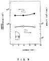
- FIGs. 9 and 10shows the two-dimensional distributions of the carrier concentration and the mobility. The results of the present invention are shown in Fig. 9, and those of the control are shown in Fig. 10, in which the carrier concentration is represented by o, and the mobility is represented by o.
- the GaN according to the present inventionexhibits very good values: a carrier concentration of 4 x 10 16 /cm 3 and a mobility of about 600 cm 2 /V•sec.
- GaN of Comparative Example 1 using AlN as the buffer layerexhibited a carrier concentration of 1 x 10 18 /cm 3 and a mobility of bout 90 cm 2 /V•sec.
- a GaN epitaxial layerwas grown on a Ga 0.5 Al 0.5 N buffer layer following the same procedures as in Example 1 except that the buffer layer was formed to have a film thickness of 0.02 ⁇ m in the step (7) of forming the buffer layer.
- TMG and TMAwere flowed at flow rates of 2.7 ⁇ 10 -5 mol/min and 2.7 x 10 -5 mol/min, respectively, for 0.5 minutes each in addition to ammonia and H 2 gases from the reaction gas injection pipe 4.
- this GaN epitaxial layeralso had an excellent X-ray rocking curve.
- the surface morphology of the layer obtained by microscopic observationwas equivalent to that of Example 1, and its carrier concentration and mobility were intermediate between those of Example 1 and Control 1.
- a gallium nitride epitaxial layerwas grown following the same procedures as in Example 1 except that the growth temperature of a buffer layer was set at 600°C in the step (6) and the gas flow time was changed to 2.5 minutes in the step (7) so that the buffer layer was formed to have a film thickness of 0.05 ⁇ m.
- this gallium nitride epitaxial layerwas equivalent to that of Example 1, and the full-width at half maximum of its X-ray rocking curve was three minutes, indicating good crystallinity.
- both of the carrier concentration and the mobility of the layerwere equivalent to those of Example 1.
- a gallium nitride epitaxial layerwas grown following the same procedures as in Example 1 except that the growth temperature of a buffer layer was set at 800 °C in the step (6).
- this GaN epitaxial layerwas equivalent to that of Example 1, and the full-width at half maximum of its X-ray rocking curve was three minutes, indicating good crystallinity.
- both of the carrier concentration and the mobility of the layerwere equivalent to those of Example 1.
- a 0.02- ⁇ m thick Ga 0.5 Al 0.5 N buffer layerwas formed on a sapphire substrate according to Example 2 and a 4- ⁇ m thick Ga 0.5 Al 0.5 N epitaxial layer was grown on the buffer layer following the same procedures as in Example 1 except that in the step (9), TMA gas and TMG gas were supplied at flow rates of 2.7 x 10 -5 mol/min and 2.7 ⁇ 10 -5 mol/min, respectively, for 60 minutes in addition to ammonia and H 2 gases from the reaction gas injection pipe 4.
- Mg as a p-type impuritywas doped in a GaN epitaxial layer while Cp 2 Mg (biscyclopentadienylmagnesium) gas was flowed in addition to ammonia gas, H 2 gas, and TMG gas, thereby growing a p-type GaN epitaxial layer to have a film thickness of 4.0 ⁇ m.
- a 0.02- ⁇ m thick GaN buffer layerwas formed on a sapphire substrate, and the 4.0- ⁇ m thick p-type GaN epitaxial layer doped with 10 20 /cm 3 of Mg was grown on the buffer layer.
- This p-type GaN epitaxial layeralso had a surface morphology equivalent to that of Example 1.
- the layerhad a hole carrier concentration of 2.0 x 10 15 /cm 3 and a mobility of 9.4 cm 2 /V•sec, i.e., exhibited p-type characteristics for the first time as a gallium nitride-based compound semiconductor. This indicates that the crystallinity of this epitaxial film is very good.
- Example 6Following the same procedures as in Example 6, a 0.02- ⁇ m thick GaN buffer layer was formed on the 4- ⁇ m thick GaN epitaxial layer obtained by the same procedure as in Example 1, and a 4.0- ⁇ m thick p-type GaN epitaxial layer doped with 10 20 /cm 3 of Mg was grown on the buffer layer.
- This p-type epitaxial layeralso had a surface morphology equivalent to that in Example 1 and had a carrier concentration of 3.5 x 10 15 /cm 3 and a mobility of 8.5 cm 2 /V•sec, i.e., similarly exhibited p-type characteristics.
- Si as an n-type impuritywas doped in a GaN epitaxial layer while silane (SiH 4 ) gas was flowed in addition to ammonia gas, H 2 gas, and TMG gas, thereby growing the layer to have a film thickness of 4.0 ⁇ m.
- a 0.02- ⁇ m thick GaN buffer layerwas formed on a sapphire substrate, and the 4- ⁇ m thick n-type GaN epitaxial layer doped with about 10 20 /cm 3 of Si was grown on the buffer layer.
- This n-type GaN epitaxial layeralso had a surface morphology equivalent to that in Example 1 and exhibited a very high carrier concentration of 1.0 x 10 19 /cm 3 .
- An AlN buffer layerwas formed on a sapphire substrate by doping Si following the same procedures as in Example 8 except that the buffer layer was formed to have a film thickness of 0.02 ⁇ m, and a 4- ⁇ m thick n-type GaN epitaxial layer was formed on the buffer layer.
- the carrier concentration of this n-type GaN epitaxial layerwas 5.0 x 10 18 /cm 3 , i.e., low compared to Control 1. It is assumed that this low carrier concentration was caused by compensation by the impurity.
- TMGtrimethylgallium
- Cp 2 Mgbiscyclopentadienylmagnesium
- step (9)after the temperature of the susceptor rose to 1,000 °C, TMG gas and Cp 2 Mg gas were supplied in addition to the ammonia and H 2 gases from the reaction gas injection pipe 4, thereby growing a p-type GaN epitaxial layer to have a film thickness of 4.0 ⁇ m.
- the 0.04- ⁇ m thick GaN buffer layer doped with Mg as a p-type impuritywas formed on a sapphire substrate, and the 4- ⁇ m thick p-type GaN epitaxial layer doped with Mg was grown on the buffer layer. Note that the doping amount of Mg was 10 20 /cm 3 in both the buffer and p-type epitaxial layers.
- An electron beam irradiation treatmentwas performed under the condition that acceleration voltage was maintained at 5 kV on the entire surface of the p-type GaN epitaxial layer obtained in Example 9, thus further imparting p conductivity type to a layer with a thickness of about 0.2 ⁇ m from the surface.
- the obtained p-type GaN epitaxial layerwas subjected to a Hall measurement.
- the carrier concentration, the resistivity, and the Hall mobilitywere improved to 4.6 x 10 18 /cm 3 , 0.3 ⁇ •cm, and 11.0 cm 2 /V•sec, respectively.
- a buffer layer and a p-type GaN epitaxial layer doped with 10 20 /cm 3 of Mgwere grown to have thicknesses of 0.04 ⁇ m and 4 ⁇ m, respectively, following the same procedures as in Example 9 except that no Mg was doped in the buffer layer. Thereafter, following the same procedures as in Example 10, an electron beam radiation was performed to further impart p conductivity type to a layer with a thickness of about 0.2 ⁇ m from the surface.
- the results of Hall measurementwere a carrier concentration of 3 x 10 17 /cm 3 , a resistivity of 2 ⁇ •cm, and a Hall mobility of 10 cm 2 /V•sec in the layer 0.2 ⁇ m thick from the surface.
- Ga X Al 1-X N (0.5 ⁇ X ⁇ 1) as a buffer layerdrastically improves the crystallinity of an epitaxial layer of a compound represented by the formula Ga X Al 1-X N (0 ⁇ X ⁇ 1) grown on the buffer layer.
- a mobility of 600 cm 2 /V ⁇ secis the most excellent value of the epitaxial layer.
- the Mg-doped GaN epitaxial layer grown on the buffer layerexhibits p conductivity type without performing any treatment. This is the phenomenon never encountered in conventional techniques, which indicates that the crystallinity of the epitaxial layer of the gallium nitride-based compound semiconductor grown by the method of the present invention is very excellent. Also, Si-doped n-type GaN grown on the buffer layer has a carrier concentration much higher than that of GaN using AlN as a buffer layer.
- the conditions under which the buffer layer of the present invention is to be grownare less severe than those for a conventional AlN buffer layer. That is, the crystallinity of an epitaxial layer of the compound represented by the formula Ga X Al 1-X N (0 ⁇ X ⁇ 1) grown on a buffer layer is good over a wide range of buffer layer thickness. This results in a high productivity in the manufacture of light-emitting devices.
- the carrier concentration and the resistivity of the layerrespectively reach practical levels to improve the performance of the layer to be 100 times or more that of the conventional example.
- the carrier concentration of the layeris improved to be nearly 1,000 times.
- the use of the technique of the present inventionmakes it possible to utilize crystals of an epitaxial layer of a compound represented by the formula Ga x Al 1-x N (0 ⁇ X ⁇ 1) over a wide range of applications from a blue light-emitting diode to a semiconductor laser at practical levels.
Landscapes
- Engineering & Computer Science (AREA)
- Chemical & Material Sciences (AREA)
- Manufacturing & Machinery (AREA)
- Physics & Mathematics (AREA)
- Computer Hardware Design (AREA)
- Microelectronics & Electronic Packaging (AREA)
- Power Engineering (AREA)
- Condensed Matter Physics & Semiconductors (AREA)
- General Physics & Mathematics (AREA)
- Materials Engineering (AREA)
- Crystallography & Structural Chemistry (AREA)
- Metallurgy (AREA)
- Organic Chemistry (AREA)
- Inorganic Chemistry (AREA)
- Chemical Kinetics & Catalysis (AREA)
- General Chemical & Material Sciences (AREA)
- Led Devices (AREA)
- Semiconductor Lasers (AREA)
Description
- The present invention relates to a method of growing crystals of a gallium nitride-based compoundsemiconductor on a substrate consisting of, e.g., sapphire and, more particularly, to a method of growing anepitaxial layer of a gallium nitride-based compound semiconductor with a high crystallinity.
- Recently, a blue light-emitting device using a gallium aluminium nitride-based compound semiconductor,e.g., a compound represented by the formula GaXAℓ1-XN (0 ≦ X ≦ 1) has attracted attention.
- As a method of growing crystals of such a gallium nitride-based compound semiconductor, ametalorganic chemical vapor deposition method (to be referred to as an MOCVD method hereinafter) is wellknown. In this method, an organometallic compound gas is supplied as a reaction gas into a reactor inwhich a sapphire substrate is placed, and the surface temperature of the substrate is held at a hightemperature of 900°C to 1,100°C, thereby growing an epitaxial layer of compound semiconductor on thesubstrate. For example, when a GaN epitaxial layer is to be grown, trimethylgallium gas and ammonia gasare used as a Ga-containing gas and an N-containing gas, respectively.
- In order to use the grown expitaxial layer of a gallium nitride-based compound semiconductor as a light-emittingdevice, it is essential to improve the crystallinity of the layer first.
- On the surface of the expitaxial layer of GaAIN, formed directly on the sapphire substrate using theMOCVD method, numerous projections and recesses are produced in the form of a hexagonal pyramid-likeor hexagonal pillar-like growth pattern. For this reason, crystal surface morphology is very poor in theobtained crystal. Therefore, it is almost impossible to fabricate a blue light-emitting device using asemiconductor crystal layer having numerous projections and recesses on its surface and a very poorsurface morphology because the yield is very low.
- In order to solve the above problems, each of Appl. Phys. Lett. 48, (1986), page 353 and PublishedUnexamined Japanese Patent Application No. 2-229476, for example, proposes a method of growing an AINbuffer layer on a substrate before growth of an expitaxial layer of a gallium nitride-based compoundsemiconductor. In this method, an AIN buffer layer with a film thickness of 100 to 500Å is formed on asapphire substrate at a relatively low growth temperature of 400 °C to 900 °C. According to this method, thecrystallinity and the surface morphology of a GaAIN expitaxial layer can be improved to some extent bygrowing the GaAIN expitaxial layer on the AIN layer as a buffer layer.
- Equally DE-OS 40 06 449 discloses the vapor deposition of an AlxGa1-xN layer onto an AIN bufferlayer. The buffer layer is formed at a growth temperature of between 380 and 800°C and has a thickness of10.0 - 50.0 nm.
- In this method, however, it is necessary to strictly restrict the growth conditions of the buffer layer. Inparticular, the film thickness must be strictly set at a very small value of 100 to 500Å. In addition, it isdifficult to uniformly form the buffer layer with a predetermined film thickness on the entire surface of large-areasapphire substrate, e.g., a sapphire substrate about 50 mm in diameter. Therefore, it is difficult toimprove the crystallinity and the surface morphology of a GaAℓN epitaxial layer formed on the buffer layerwith a high yield. Furthermore, the obtained crystallinity is still unsatisfactory to form a practical light-emittingdiode or semiconductor laser, i.e., it requires further improvements.
- In addition, this method cannot realize a p-n junction sufficient to put a light-emitting diode or the likeinto practical use. In general, when a light-emitting device is to be fabricated by forming a compoundsemiconductor layer on a substrate, doping a small amount of an impurity in the compound semiconductorto form an n- or p-type layer and in this manner obtain a p-n junction is known as a very effective means ofimproving the luminance of the device. However, no blue light-emitting device which realizes a sufficientluminance has been developed yet. The reason for this is that p conductivity type of a semiconductorcrystal film cannot be formed.
- It is difficult for conventional methods to form a p-type semiconductor crystal film even if p-typeimpurities such as Zn and Mg may be doped in a GaAℓN epitaxial layer, because the crystal film hasextremely bad crystallinity. For this reason, conventionally, n-type GaN is grown on a sapphire substrate by,e.g., Halide Vapor Phase Epitaxial (HVPE) crystal growth method, Zn diffusion is Performed for the grownlayer, and an I layer is formed to fabricate a blue light-emitting device with an MIS structure. However, alight-emitting device fabricated by this method cannot realize a satisfactory luminance efficiency.
- In a recently reported technique, in order to formp conductivity type of a semiconductor crystal film,Mg is doped in GaN epitaxial layer, and then an electron beam is radiated on the GaN layer (Oyo Butsuri,1991, Vol. 60, February, pp. 163 to 166). In this technique, the MOCVD method is used to form an AℓNbuffer layer with a thickness of 0.02 to 0.05 µm on a sapphire substrate at a low temperature (about 400 °Cto 600°C). Subsequently, the temperature is increased to 1,000°C. An Mg-doped GaN layer is then grownon the AℓN buffer layer, and an electron beam is radiated on the surface to form a p-type Mg-doped GaN layer.
- This method, however, is still far from a practical level. That is, the characteristics of the disclosed p-typeGaN layer are only a maximum free hole concentration (carrier concentration) of 1017/cm3 and aminimum resistivity of 12 Ω·cm.
- The present invention has been made in consideration of the above situation and has as its object toprovide a method which can grow a gallium nitride-based compound semiconductor having crystallinity andsurface morphology at practical levels, with high stability and high yield while using a buffer layer.
- It is another object of the present invention to provide a method which can grow a p- or n-typesemiconductor layer at an excellent practical level so as to allow formation of an excellent p-n junction in aGaAℓN for use in a light-emitting device.
- According to the present invention this object is achieved with a method according to
Claim 1. - Further preferred embodiments ofthe invention are claimed in the
dependent claims 2 to 16. - According to the present invention, a buffer layer and/or a gallium nitride-based compound semiconductorlayer can be doped with an n- or p-type impurity on a substrate on the obtained buffer layer.
- This invention can be more fully understood from the following detailed description when taken inconjunction with the accompanying drawings, in which:
- Fig. 1 is a schematic sectional view showing the structure of an epitaxial wafer according to the crystalgrowth method of the present invention;
- Fig. 2 is a schematic sectional view showing the structure of an epitaxial wafer according to aconventional crystal growth method;
- Fig. 3 is a graph showing the relationship between the full width at half-maximum (FWHM) of the double-crystalrocking curve of a GaN epitaxial layer and the film thickness of a buffer layer;
- Fig. 4 is a microphotograph showing the structure of crystals of a GaN epitaxial layer;
- Fig. 5 is a microphotograph showing the structure of crystals of another GaN epitaxial layer;
- Fig. 6 is a microphotograph showing the structure of crystals of still another GaN epitaxial layer;
- Fig. 7 is a microphotograph showing the structure of crystals of still another GaN epitaxial layer;
- Fig. 8 is a partial schematic sectional view showing an apparatus used in the present invention;
- Fig. 9 is a graph showing the two-dimensional distributions of the carrier concentration and the mobilityobtained by Hall measurement of GaN crystals according to the present invention;
- Fig. 10 is a graph showing the two-dimensional distributions of the carrier concentration and the mobilityobtained by Hall measurement of conventional GaN crystals;
- Fig. 11 is a sectional view showing the structure of an embodiment of an element using a semiconductorcrystal film according to the present invention; and
- Fig. 12 is a sectional view showing the structure of another embodiment of the element.
- The present invention will be described below.
- The surface layer preferably consists of a gallium nitride-based compound.
- The thickness of the buffer layer is preferably 0.001 µm to 0.2µm. If the thickness is smaller than 0.001 µm or larger than 0.5 µm, the surface morphology of the epitaxiallayer gallium nitride-based compound formed on the buffer layer tends to be deteriorated.
- The first temperature is adjusted to 400°C to 800°C.If the temperature is lower than 200 °C, it becomes difficult to form the buffer layer. If the temperature ishigher than 900 ° C, the buffer layer becomes monocrystalline and therefore no longer performs functions asa buffer layer.
- The epitaxial layer of the compound formed on the buffer layer is represented by the formula GaXA1-XN(note that X falls within the range of 0 ≦ X ≦ 1).
- Fig. 1 is a sectional view showing the structure of an epitaxial wafer obtained when a semiconductorlayer represented by the formula GaXAl1-XN (0 ≦ X ≦ 1) are grown on a buffer layer consisting ofGaXAℓ1-XN (0.5 < X ≦ 1). Fig. 2 is a sectional view showing the structure of wafer obtained when a gallium nitride-based semiconductor layer is grown on an AℓN buffer layer.
- The allowable thickness range of the buffer layer of the present invention is wider than those ofconventional buffer layers. For this reason, it is possible to grow the buffer layer and the semiconductorlayer of the compound represented by the formula GaXAl1-XN (0 ≦ X ≦ 1) with high yield.
- A method of growing a gallium nitride-based compound semiconductor layer using AℓN as a bufferlayer is described in detail in, e.g., Thin Solid Films, 163, (1988), page 415, or Appl. Phys. Lett. 48, (1986),page 353. The effects of the buffer layer described in these references will be briefly described below.
- AℓN which is grown at a low temperature (about 600°C) is a polycrystalline layer. When thetemperature of a substrate on which this AℓN polycrystalline layer is formed is increased to about 1,000°Cin order to form, e.g., GaN, this polycrystalline layer partially becomes monocrystalline. The monocrystallineportion serves as a seed crystal with an uniform orientation. When GaN epitaxial layer is grown at 1,000 °C,GaN epitaxial layer is grown from this seed crystal to make it possible to grow an uniform GaN epitaxiallayer. If no buffer layer is used, the sapphire substrate itself serves as a seed crystal. Since, in this caseevery surface portions of the sapphire substrate serve as a seed crystal, there is a large variation in crystalorientations of GaN hexagonal pillars grown on the sapphire substrate.
- By comparing the case in which GaXAℓ1-XN (0.5 ≦ X ≦ 1) is formed as a buffer layer as in the presentinvention with the case in which conventional AℓN is used as the buffer layer, the following assumption canbe made.
- First, suppose that GaN of, e.g., X = 1 is formed as the buffer layer. In this case, the melting point ofGaN is 1,100 °C and the melting point of Aℓ N is 1,700 ° C. When a buffer layer of GaN is formed at 600 °C,a polycrystalline layer results. Subsequently, when the temperature of the substrate is increased to 1,000°Cin order to grow a GaN epitaxial layer on this polycrystalline GaN layer, the GaN buffer layer partiallybecomes monocrystalline. As in the case wherein AℓN is used as a buffer layer, this monocrystallineportion serves as a seed crystal for a GaN epitaxial layer.
- It is assumed that the following advantages can be obtained by the present invention compared with thecase in which the AℓN buffer layer is formed.
- First, since the melting point is low, conversion into single-crystals easily occurs during the rise of thetemperature. Therefore, the effects as a buffer layer can be expected even when the thickness of the bufferlayer is increased.
- Secondary, the buffer layer consists of GaN. As a result, an improvement in crystallinity can beexpected when the GaN epitaxial layer is grown on the buffer layer because the epitaxial layer is formed onthe layer of the same material.
- To confirm the above advantages, three types of buffer layers consisting of AℓN, Ga0.5Aℓ0.5N, and GaNwere independently formed on sapphire substrates at 600°C, and a 4-µm thick GaN epitaxial layer wasgrown on each of the formed layers at 1,000°C. A measurement was made for the full width at half-maximum(FWHM) of the double-crystal X-ray rocking curve of each GaN epitaxial layer. Fig. 3 is a graphshowing the relationship between the FWHM and the film thickness of the buffer layer. In Fig. 3, the smallerthe FWHM is, the better the crystallinity.
- As shown in Fig. 3, it was found that when GaN was formed as the buffer layer, a better crystallinitycould be obtained over a wide film thickness range of the buffer layer, and that the effect of Ga0.5Aℓ0.5Nwas intermediate of the three cases. This indicates that the advantages assumed above are correct.
- Figs. 4 to 7 are microphotographs showing the structures of the surfaces of GaN epitaxial layersobtained when GaN buffer layers having different film thicknesses were formed on sapphire substrates and4-µm thick GaN epitaxial layer were grown on the respective buffer layers. The thicknesses of the bufferlayers shown in Figs. 4 to 7 are 0.002 µm, 0.07 µm, 0.20 µm, and 0 µm (no buffer layer) in this order.
- As can be seen from these drawings, hexagonal crystal pillars appear on the surface when no bufferlayer is formed. Although it depends on the formation conditions of the buffer layer, the surface of the bufferlayer tends to have a mirror surface uniformity as the formation of the buffer layer advances. However,when the buffer layer is too thick, the surface state (surface morphology) is deteriorated. A preferablethickness of the buffer layer is, therefore, 0.01 µm to 0.2 µm.
- The temperature at which an epitaxial layer of the compound represented by the formula GaXAl1-XN (0≦ X ≦ 1) are formed on the buffer layer is 900°C to 1150°C. If the temperature is less than900°C, gallium nitride-based compound tends to become polycrystalline. If the temperature exceeds1150°C, gallium nitride crystals tend to decompose during growing.
- The buffer layer according to the crystal growth method of the present invention can be formed not onlyon a sapphire substrate but also on any layer as long as the layer has an epitaxial semiconductor layer of acompound represented by the formula GaXAl1-XN (0 ≦ X ≦ 1). Thus, according to the present invention thegallium nitride-based compound semiconductor can form a multi layer structure such as buffer/epitaxial/buffer/epitaxial structure and buffer/epitaxial/epitaxial/buffer/epitaxial structure.
- For example, when it is desired to form a p-type GaN epitaxial layer doped with Mg as a p-typeimpurity on an n-type GaN epitaxial layer, it is also possible to form a buffer layer on the n-type GaNepitaxial layer and to form the p-type GaN epitaxial layer on the buffer layer.
- According to the present invention, the buffer layer and/or the epitaxial layer of the compoundrepresented by the formula GaXAl1-XN (0 ≦ X ≦ 1) formed on the buffer layer can be doped with an n- or p-typeimpurity.
- More specifically, this growth method of the present invention is a method of supplying a reaction gasinto a reactor to grow an epitaxial layer consisting of an n- or p-type gallium nitride compound. Thecharacteristic feature of this method is that before the growth of the epitaxial layer, an n- or p-type impurityis doped in a buffer layer represented by the formula GaxAℓ1-xN (0.5 ≦ X ≦ 1) to grow a polycrystallinelayer at a first temperature of 400°C to 800°C, and then an n- or p-type impurity is doped inthe surface of the buffer layer at a second temperature of 900°C to 1150°C or more to growan epitaxial layer of a compound represented by the formula GaXAl1-XN (0 ≦ X ≦ 1).
- As the impurity to be doped in the compound represented by the formula GaXAl1-XN (0 ≦ X ≦ 1) toimpartn conductivity type to it, it is possible to use, for example, Si and Sn. Examples of the impurity forimpartingp conductivity type to the compound represented by the formula GaXAl1-XN (0 ≦ X ≦ 1) are Zn,Mg, Ca, and Be. In the growth method of the present invention, the impurity for impartingn orpconductivity type to the gallium nitride-based compound is not particularly limited. In the method of thepresent invention, it is possible to dope any impurity which is presently, already used or may be developedin the future in order to impartp orn conductivity type to the gallium nitride-based compound semiconductor.
- The concentration of the impurity to be doped in the semiconductor crystal film is preferably as largeas possible because the resistance of a semiconductor crystal film decreases when an impurity is heavilydoped in it. A concentration at which the impurity can be doped without deteriorating the crystallinity of theepitaxial layer is preferably 1017 to 1020 cm3.
- The thickness of the buffer layer is 0.001 to 0.2 µm. Ifthe thickness is less than 0.001 µm or more than 0.5 µm, the surface state and the crystallinity of theepitaxial layer of the n- or p-type gallium nitride-based compound formed on the surface of the buffer layertend to deteriorate. For example, hexagonal crystal pillars appear on the surface of the semiconductorcrystal film when no buffer layer is present. The crystal surface tends to have a mirror surface uniformity asthe formation of a buffer layer proceeds though it depends on the formation conditions of the buffer layer.However, if the buffer layer is too thick, the surface state and the crystallinity of the semiconductor crystalfilm again tend to deteriorate.
- According to the crystal growth method of the present invention, it is possible to form an epitaxial layerof a p-type compound represented by the formula GaXAl1-XN (0 ≦ X ≦ 1) on the surface of a buffer layerdoped with, e.g., a p-type impurity and to radiate an electron beam onto this epitaxial layer. The p-typegallium nitride-based compound semiconductor manufactured by this method has a large electron-beamradiating effect and can provide a particularly excellent p-type epitaxial layer as compared with a p-typeepitaxial layer stacked on a buffer layer not doped with any p-type impurity.
- According to the growth method of the present invention, a p-type GaN epitaxial layer can be grownthrough the following steps.
- First, an Mg-doped polycrystalline buffer layer is grown at a low temperature of 400°C to 800°C.Subsequently, in order to grow an epitaxial layer of Mg-doped p-type GaN on the surface of the bufferlayer, the temperature is raised to about 1,000° C. At this time, the buffer layer partially becomesmonocrystalline to form a seed crystal for growing p-type GaN.
- The manner of this conversion into single crystals will be described in more detail below. During thetemperature rise to 1,000°C, Mg in the buffer layer causes rearrangement to a Ga lattice site to facilitate itsentrance into the Ga site. Therefore, when the temperature is raised to 1,000°C and the Mg-doped p-typeGaN epitaxial layer is grown, the buffer layer in which Mg enters the Ga site serves as a seed crystal tomake it easier for Mg to enter a Ga site in the p-type GaN epitaxial layer to be grown on the surface of thebuffer layer.
- As described above, doping Mg in the buffer layer facilitates formation of an epitaxial layer of a p-typegallium nitride-based compound, which is difficult to perform in conventional methods.
- The compound semiconductor epitaxial layer represented by the formula GaXAl1-XN (0 ≦ X ≦ 1) has aproperty to acquiren conductivity type without being doped with an impurity such as Si. For this reason, itis not always necessary to dope Si in the semiconductor crystal film in order to impartn conductivity typeto the gallium nitride-based compound semiconductor. However, when a gallium nitride-based compound semiconductor is grown on the surface of a buffer layer doped with an n-type impurity, an n-type epitaxiallayer having more preferable characteristics can be formed.
- Figs. 11 and 12 are sectional views showing the structures of light-emitting diodes of an embodimentaccording to the present invention. As illustrated in the embodiment of Figs. 11 and 12, a buffer layer dopedwith an impurity may be formed not only on the sapphire substrate but also on any layer.
- The reaction gas used in the present invention preferably contains at least one material selected fromthe group consisting of trimethylgallium, trimethylaluminum and triethyl aluminum. This reaction gas alsopreferably contains at least one material selected from the group consisting of ammonia gas and hydrazine.This reaction gas also more preferably contains at least one gas selected from the group consisting oftrimethylindium, cyclopentadienyl-magnesium, diethyzinc, and trimethylzinc.
- The substrate is selected from the group consisting of sapphire, Si, SiC, GaP, InP and GaAs.
- Examples of the present invention will be described below. However, the following Examples merelyexemplify the method of practicing the technical concept of the present invention. Therefore, the method ofthe present invention is not particularly limited to the Examples below in terms of, e.g., the growthconditions, the type of an organometallic compound gas, and the materials used. Various modifications canbe made for the growth method of the present invention in accordance with the scope of claims.
- An apparatus shown in Fig. 8 was used to perform crystal growth of a gallium nitride-based compoundsemiconductor.
- A GaN epitaxial layer was grown to have a film thickness of 4 µm on a sapphire substrate inaccordance with the following steps.
- (1) A washed sapphire substrate having a diameter of 2 inches was placed on a
susceptor 2. - (2) The air in a
stainless steel reactor 1 was sufficiently exhausted by anexhaust pump 6, and H2 gaswas introduced into thereactor 1, thus replacing the air in the reactor with H2 gas. - (3) Thereafter, the
susceptor 2 was heated up to 1,060 ° C by a heater 3 while supplying H2 gas into thereactor 1 from a reactiongas injection pipe 4 and aninjection subpipe 5 in the upper portion of thereactor 1. - (4) This state was held for 10 minutes to remove an oxide film from the surface of the sapphiresubstrate.
- (5) The temperature of the
susceptor 2 was then decreased to 500°C, and the substrate was left tostand until the temperature became stable. - (6) Subsequently, a gas mixture of H2 and N2 was supplied from the
injection subpipe 5, and a gasmixture of ammonia gas and H2 gas was supplied from the reactiongas injection pipe 4. The flow rate ofeach of the H2 and N2 gases supplied from theinjection subpipe 5 was 10 ℓ/min, and the flow rates ofthe ammonia gas and the H2 gas supplied from the reactiongas injection pipe 4 were 4 ℓ/min and 1ℓ/min, respectively. This state was maintained until the temperature of thesusceptor 2 was stabilized at500°C. - (7) Thereafter, in order to form a buffer layer, TMG (trimethylgallium) gas was flowed at a flow rate of 2.7x 10⁻⁵ mol/min for one minute in addition to the ammonia and H2 gases from the reaction
gas injectionpipe 4. - (8) Subsequently, only the TMG gas was stopped to stop the growth of the buffer layer. The result was a0.02-µm thick buffer layer. The temperature of the
susceptor 2 was increased to 1,020 °C while flowingthe other gases. - (9) After the temperature of the
susceptor 2 was raised to 1,020°C, TMG gas was flowed at a flow rateof 5.4 x 10⁻⁵ mol/min for 60 minutes in addition to the ammonia and H2 gases from the reactiongasinjection pipe 4, thereby growing a GaN epitaxial layer to have a film thickness of 4.0 µm. - During the growth, the H2 and N2 gases were constantly supplied from the
injection subpipe 5 underthe conditions described above so that the interior of the reactor was not contaminated with the reactiongas. In addition, thesusceptor 2 was rotated at a rate of 5 rpm by a motor 7 so as to uniformly growcrystals. Note that while the gases were supplied, the supplied gases were exhausted outside from anexhaust pipe 8 branched from piping of theexhaust pump 6. - In this manner, the 0.02-µm thick GaN buffer layer and the 4-µm thick GaN epitaxial layer were grownon the sapphire substrate.
- A 4-µm thick GaN epitaxial layer was grown on an AℓN buffer layer following the same procedures asin Example 1 except that the AℓN buffer layer was formed to have a film thickness of 0.02 µm in the step(7) of forming the buffer layer.
- In the formation of the AℓN buffer layer, TMA (trimethylaluminum) was flowed at a flow rate of 2.7 x10⁻⁵ mol/min in addition to ammonia and H2 gases from the reaction
gas injection pipe 4 in the step (7). - After the growth, a Hall measurement was performed at room temperature to obtain the carrierconcentration and the mobility of the GaN epitaxial layer according to the present invention and those of theGaN epitaxial layer of
Control 1. Each of Figs. 9 and 10 shows the two-dimensional distributions of thecarrier concentration and the mobility. The results of the present invention are shown in Fig. 9, and those ofthe control are shown in Fig. 10, in which the carrier concentration is represented by o, and the mobility isrepresented by o. - Referring to Figs. 9 and 10, in the case of growth of nondoped crystals, as the carrier concentrationdecreases and the mobility increases, the crystallinity is improved and the impurity concentration isdecreased.
- As is apparent from Fig. 9, the GaN according to the present invention exhibits very good values: acarrier concentration of 4 x 10¹⁶/cm3 and a mobility of about 600 cm2/V•sec.
- As is apparent from Fig. 10, GaN of Comparative Example 1 using AℓN as the buffer layer exhibited acarrier concentration of 1 x 10¹⁸/cm3 and a mobility of bout 90 cm2/V•sec.
- A GaN epitaxial layer was grown on a Ga0.5Aℓ0.5N buffer layer following the same procedures as inExample 1 except that the buffer layer was formed to have a film thickness of 0.02 µm in the step (7) offorming the buffer layer.
- In the formation of the buffer layer, TMG and TMA were flowed at flow rates of 2.7 × 10⁻⁵ mol/min and2.7 x 10-5 mol/min, respectively, for 0.5 minutes each in addition to ammonia and H2 gases from thereaction
gas injection pipe 4. - As shown in Fig. 3, this GaN epitaxial layer also had an excellent X-ray rocking curve. In addition, thesurface morphology of the layer obtained by microscopic observation was equivalent to that of Example 1,and its carrier concentration and mobility were intermediate between those of Example 1 and
Control 1. - A gallium nitride epitaxial layer was grown following the same procedures as in Example 1 except thatthe growth temperature of a buffer layer was set at 600°C in the step (6) and the gas flow time waschanged to 2.5 minutes in the step (7) so that the buffer layer was formed to have a film thickness of 0.05µm.
- The surface morphology of this gallium nitride epitaxial layer was equivalent to that of Example 1, andthe full-width at half maximum of its X-ray rocking curve was three minutes, indicating good crystallinity. Inaddition, both of the carrier concentration and the mobility of the layer were equivalent to those of Example1.
- A gallium nitride epitaxial layer was grown following the same procedures as in Example 1 except thatthe growth temperature of a buffer layer was set at 800 °C in the step (6).
- The surface morphology of this GaN epitaxial layer was equivalent to that of Example 1, and the full-widthat half maximum of its X-ray rocking curve was three minutes, indicating good crystallinity. In addition,both of the carrier concentration and the mobility of the layer were equivalent to those of Example 1.
- A 0.02-µm thick Ga0.5Aℓ0.5N buffer layer was formed on a sapphire substrate according to Example 2and a 4-µm thick Ga0.5Aℓ0.5N epitaxial layer was grown on the buffer layer following the same proceduresas in Example 1 except that in the step (9), TMA gas and TMG gas were supplied at flow rates of 2.7 x10⁻⁵ mol/min and 2.7 × 10⁻⁵ mol/min, respectively, for 60 minutes in addition to ammonia and H2 gases from the reaction
gas injection pipe 4. - The surface morphology of this 4-µm thick Ga0.5Aℓ0.5N epitaxial layer was equivalent to that of Example1.
- In the step (9), Mg as a p-type impurity was doped in a GaN epitaxial layer while Cp2Mg (biscyclopentadienylmagnesium)gas was flowed in addition to ammonia gas, H2 gas, and TMG gas, thereby growing ap-type GaN epitaxial layer to have a film thickness of 4.0 µm.
- In the manner described above, a 0.02-µm thick GaN buffer layer was formed on a sapphire substrate,and the 4.0-µm thick p-type GaN epitaxial layer doped with 1020/cm3 of Mg was grown on the buffer layer.
- This p-type GaN epitaxial layer also had a surface morphology equivalent to that of Example 1. Inaddition, the layer had a hole carrier concentration of 2.0 x 10¹⁵/cm3 and a mobility of 9.4 cm2/V•sec, i.e.,exhibited p-type characteristics for the first time as a gallium nitride-based compound semiconductor. Thisindicates that the crystallinity of this epitaxial film is very good.
- Following the same procedures as in Example 6, a 0.02-µm thick GaN buffer layer was formed on the4-µm thick GaN epitaxial layer obtained by the same procedure as in Example 1, and a 4.0-µm thick p-typeGaN epitaxial layer doped with 1020/cm3 of Mg was grown on the buffer layer.
- This p-type epitaxial layer also had a surface morphology equivalent to that in Example 1 and had acarrier concentration of 3.5 x 10¹⁵/cm3 and a mobility of 8.5 cm2/V•sec, i.e., similarly exhibited p-typecharacteristics.
- In the step (9), Si as an n-type impurity was doped in a GaN epitaxial layer while silane (SiH4) gas wasflowed in addition to ammonia gas, H2 gas, and TMG gas, thereby growing the layer to have a filmthickness of 4.0 µm.
- In the manner described above, a 0.02-µm thick GaN buffer layer was formed on a sapphire substrate,and the 4-µm thick n-type GaN epitaxial layer doped with about 1020/cm3 of Si was grown on the bufferlayer.
- This n-type GaN epitaxial layer also had a surface morphology equivalent to that in Example 1 andexhibited a very high carrier concentration of 1.0 x 10¹⁹/cm3.
- An AℓN buffer layer was formed on a sapphire substrate by doping Si following the same proceduresas in Example 8 except that the buffer layer was formed to have a film thickness of 0.02 µm, and a 4-µmthick n-type GaN epitaxial layer was formed on the buffer layer.
- The carrier concentration of this n-type GaN epitaxial layer was 5.0 x 10¹⁸/cm3, i.e., low compared to
Control 1. It is assumed that this low carrier concentration was caused by compensation by the impurity. - In the step (7), in order to form a buffer layer, TMG (trimethylgallium) gas and Cp2Mg (biscyclopentadienylmagnesium)gas were flowed in addition to ammonia gas and H2 gas from the reaction
gas injectionpipe 4, thereby forming a 0.04-µm thick buffer layer. - In the step (9), after the temperature of the susceptor rose to 1,000 °C, TMG gas and Cp2Mg gas weresupplied in addition to the ammonia and H2 gases from the reaction
gas injection pipe 4, thereby growing ap-type GaN epitaxial layer to have a film thickness of 4.0 µm. - In the manner described above, the 0.04-µm thick GaN buffer layer doped with Mg as a p-type impuritywas formed on a sapphire substrate, and the 4-µm thick p-type GaN epitaxial layer doped with Mg wasgrown on the buffer layer. Note that the doping amount of Mg was 1020/cm3 in both the buffer and p-typeepitaxial layers.
- Thereafter, a Hall measurement was performed for this p-type GaN epitaxial layer. The results were acarrier concentration of 4.5 x 10¹⁷/cm3, a resistivity of 1.0 Ω·cm, and a Hall mobility of 9.0 cm2/V•sec.
- An electron beam irradiation treatment was performed under the condition that acceleration voltage wasmaintained at 5 kV on the entire surface of the p-type GaN epitaxial layer obtained in Example 9, thusfurther imparting p conductivity type to a layer with a thickness of about 0.2 µm from the surface.
- The obtained p-type GaN epitaxial layer was subjected to a Hall measurement. As a result, in the layer0.2 µm thick from the surface, the carrier concentration, the resistivity, and the Hall mobility were improvedto 4.6 x 10¹⁸/cm3, 0.3 Ω•cm, and 11.0 cm2/V•sec, respectively.
- A buffer layer and a p-type GaN epitaxial layer doped with 1020/cm3 of Mg were grown to havethicknesses of 0.04 µm and 4 µm, respectively, following the same procedures as in Example 9 except thatno Mg was doped in the buffer layer. Thereafter, following the same procedures as in Example 10, anelectron beam radiation was performed to further impartp conductivity type to a layer with a thickness ofabout 0.2 µm from the surface.
- The results of Hall measurement were a carrier concentration of 3 x 10¹⁷/cm3, a resistivity of 2 Ω•cm,and a Hall mobility of 10 cm2/V•sec in the layer 0.2 µm thick from the surface.
- As described above, forming GaXAℓ1-XN (0.5 ≦ X ≦ 1) as a buffer layer drastically improves thecrystallinity of an epitaxial layer of a compound represented by the formula GaXAl1-XN (0 ≦ X ≦ 1) grown onthe buffer layer. For example, in a Hall measurement of crystals, a mobility of 600 cm2/V·sec is the mostexcellent value of the epitaxial layer.
- In addition, since the buffer layer is formed, the Mg-doped GaN epitaxial layer grown on the buffer layerexhibitsp conductivity type without performing any treatment. This is the phenomenon never encounteredin conventional techniques, which indicates that the crystallinity of the epitaxial layer of the gallium nitride-basedcompound semiconductor grown by the method of the present invention is very excellent. Also, Si-dopedn-type GaN grown on the buffer layer has a carrier concentration much higher than that of GaNusing AℓN as a buffer layer.
- Furthermore, the conditions under which the buffer layer of the present invention is to be grown are lesssevere than those for a conventional AℓN buffer layer. That is, the crystallinity of an epitaxial layer of thecompound represented by the formula GaXAl1-XN (0 ≦ X ≦ 1) grown on a buffer layer is good over a widerange of buffer layer thickness. This results in a high productivity in the manufacture of light-emittingdevices.
- In addition, since doping an n- or p-type impurity in a buffer layer grown at a low temperature improvesthe conductivity characteristics of a semiconductor epitaxial layer of the n- or p-type compound representedby the formula GaXAl1-XN (0 ≦ X ≦ 1) to be subsequently grown on the buffer layer, a p-n junction can beeasily formed. Table 1 below indicates how good the characteristics of the p-type epitaxial layer of thegallium nitride-based compound are.
Hole Carrier Concentration number/cm3 Resistivity (Ω•cm) Hall mobility cm3/V•sec Example 9 4.5 × 10¹⁷ 1.0 9.0 Example 10 4.6 x 10¹⁸ 0.2 11.0 Comparative Example 3 3 x 10¹⁷ 2 10.0 - As shown in Table 1, in the case of a p-type GaN epitaxial layer, the carrier concentration and theresistivity of the layer respectively reach practical levels to improve the performance of the layer to be 100times or more that of the conventional example. Especially when an electron beam is radiated onto a p-typeGaN epitaxial layer grown by the crystal growth method of the present invention, the carrier concentration ofthe layer is improved to be nearly 1,000 times.
- As has been described above, the use of the technique of the present invention makes it possible toutilize crystals of an epitaxial layer of a compound represented by the formula GaxAl1-xN (0 ≦ X ≦ 1) over awide range of applications from a blue light-emitting diode to a semiconductor laser at practical levels.
Claims (16)
- A crystal growth method for a gallium nitride compoundsemiconductor, comprising the steps of:vapor-growing a polycrystalline buffer layer representedby formula GaxAl1-xN (0.5 ≤ x ≤ 1), having a thickness of 0.001to 0.2 µm, on a substrate by metal organic chemical vapordeposition at a first temperature in the range of 400 to 800°C;andvapor-growing an epitaxial semiconductor layer represented by formulaGaxAl1-xN (0 ≤ x < 1) on said formed buffer layer by metalorganic chemical vapor deposition at a second temperaturein the range of 900°C to 1150°C.
- A method according to claim 1characterized by furthercomprising the steps of:vapor-growing another polycrystalline buffer layerrepresented by formula GaxAl1-xN (0.5 < x < 1), having athickness of 0.001 to 0.2 µm, on said gallium nitride-basedcompound semiconductor layer by metal organic chemical vapordeposition at a third temperature lower than said secondtemperature; andvapor-growing an epitaxial semiconductor layer represented by formulaGaxAl1-xN (0 ≤ x ≤ 1) on said another buffer layer by metalorganic chemical vapor deposition at a fourth temperaturehigher than said third temperature.
- A method according to claim 1,characterized by further comprising the step of doping an n- or p-typeimpurity in said buffer layer.
- A method according to claim 3,characterized in that said n-type impurity is at least one materialselected from the group consisting of Si and Sn.
- A method according to claim 3,characterized in that said p-type impurity is at least one materialselected from the group consisting of Zn, Mg, Ca, and Be.
- A method according to claim 3,characterized in that the doping amount of said n- or p-type impurity is-1017 to 1020/cm3.
- A method according to claim 1,characterized by further comprising the step of doping an n- or p-typeimpurity in said semiconductor layer.
- A method according to claim 7,characterized in that said n-type impurity is at least one materialselected from the group consisting of Si and Sn.
- A method according to claim 7,characterized in that said p-type impurity is at least one materialselected from the group consisting of Zn, Mg, Ca, and Be.
- A method according to claim 7,characterized in that the doping amount of said n- or p-type impurity is1017 to 1020/cm3.
- A method according to claim 1,characterized in that said buffer layer is grown by using a reaction gascontaining at least one gas selected from the group consisting of trimethyl gallium and triethylgallium,and at least one gas selected from the group consisting of ammonia gas and hydrazine.
- A method according to claim 11,characterized in that said reaction gas contains trimethylaluminum.
- A method according to claim 11,characterized in that said reaction gas contains at least one gasselected from the group consisting of cyclopentadienylmagnesium, diethylzinc, and trimethylzinc.
- A method according to claim 1,characterized in that said substrate comprises one material selectedfrom the group consisting of sapphire, Si, SiC and GaAs.
- A method according to claim 12,characterized by further comprising, after the formation of saidsemiconductor layer, the step of radiating an electron beam onto the formed semiconductor layer.
- A method according to claim 1,characterized in that said semiconductor layer has the samecomposition of said buffer layer and is represented by formula GaXAℓ1-XN (0.5 ≦ X ≦ 1).
Applications Claiming Priority (6)
| Application Number | Priority Date | Filing Date | Title |
|---|---|---|---|
| JP3225991 | 1991-01-31 | ||
| JP32259/91 | 1991-01-31 | ||
| JP3225991 | 1991-01-31 | ||
| JP8984091AJPH088217B2 (en) | 1991-01-31 | 1991-03-27 | Crystal growth method for gallium nitride-based compound semiconductor |
| JP8984091 | 1991-03-27 | ||
| JP89840/91 | 1991-03-27 |
Publications (3)
| Publication Number | Publication Date |
|---|---|
| EP0497350A1 EP0497350A1 (en) | 1992-08-05 |
| EP0497350B1 EP0497350B1 (en) | 1995-08-02 |
| EP0497350B2true EP0497350B2 (en) | 2002-01-09 |
Family
ID=26370800
Family Applications (1)
| Application Number | Title | Priority Date | Filing Date |
|---|---|---|---|
| EP92101560AExpired - LifetimeEP0497350B2 (en) | 1991-01-31 | 1992-01-30 | Crystal growth method for gallium nitride-based compound semiconductor |
Country Status (3)
| Country | Link |
|---|---|
| EP (1) | EP0497350B2 (en) |
| JP (1) | JPH088217B2 (en) |
| DE (1) | DE69203736T3 (en) |
Cited By (5)
| Publication number | Priority date | Publication date | Assignee | Title |
|---|---|---|---|---|
| US6610606B2 (en) | 2001-03-27 | 2003-08-26 | Shiro Sakai | Method for manufacturing nitride compound based semiconductor device using an RIE to clean a GaN-based layer |
| US6861270B2 (en) | 2000-06-01 | 2005-03-01 | Shiro Sakai | Method for manufacturing gallium nitride compound semiconductor and light emitting element |
| US6884647B2 (en) | 2000-09-22 | 2005-04-26 | Shiro Sakai | Method for roughening semiconductor surface |
| US7015511B2 (en) | 2001-06-29 | 2006-03-21 | Nitride Semiconductors Co., Ltd. | Gallium nitride-based light emitting device and method for manufacturing the same |
| US7951617B2 (en) | 2005-10-06 | 2011-05-31 | Showa Denko K.K. | Group III nitride semiconductor stacked structure and production method thereof |
Families Citing this family (100)
| Publication number | Priority date | Publication date | Assignee | Title |
|---|---|---|---|---|
| JPH088217B2 (en)† | 1991-01-31 | 1996-01-29 | 日亜化学工業株式会社 | Crystal growth method for gallium nitride-based compound semiconductor |
| JP2751963B2 (en)* | 1992-06-10 | 1998-05-18 | 日亜化学工業株式会社 | Method for growing indium gallium nitride semiconductor |
| US5393993A (en)* | 1993-12-13 | 1995-02-28 | Cree Research, Inc. | Buffer structure between silicon carbide and gallium nitride and resulting semiconductor devices |
| US5656832A (en)* | 1994-03-09 | 1997-08-12 | Kabushiki Kaisha Toshiba | Semiconductor heterojunction device with ALN buffer layer of 3nm-10nm average film thickness |
| JP2007184645A (en)* | 1994-08-22 | 2007-07-19 | Rohm Co Ltd | Manufacturing method of semiconductor light emitting element |
| KR960007835A (en)* | 1994-08-22 | 1996-03-22 | 강박광 | Manufacturing method of blue luminescent gallium nitride laminated film |
| US6996150B1 (en) | 1994-09-14 | 2006-02-07 | Rohm Co., Ltd. | Semiconductor light emitting device and manufacturing method therefor |
| US5523589A (en)* | 1994-09-20 | 1996-06-04 | Cree Research, Inc. | Vertical geometry light emitting diode with group III nitride active layer and extended lifetime |
| US5843590A (en)* | 1994-12-26 | 1998-12-01 | Sumitomo Electric Industries, Ltd. | Epitaxial wafer and method of preparing the same |
| JP3564645B2 (en)* | 1995-01-27 | 2004-09-15 | 株式会社日鉱マテリアルズ | Gallium nitride based semiconductor crystal growth method |
| JPH08264836A (en)* | 1995-03-27 | 1996-10-11 | Sumitomo Electric Ind Ltd | Compound semiconductor light emitting device and manufacturing method thereof |
| JPH08264835A (en)* | 1995-03-27 | 1996-10-11 | Sumitomo Electric Ind Ltd | Compound semiconductor light emitting device and manufacturing method thereof |
| TW290743B (en)* | 1995-03-27 | 1996-11-11 | Sumitomo Electric Industries | |
| JP2795226B2 (en)* | 1995-07-27 | 1998-09-10 | 日本電気株式会社 | Semiconductor light emitting device and method of manufacturing the same |
| JPH0983017A (en)* | 1995-09-08 | 1997-03-28 | Sumitomo Electric Ind Ltd | Epitaxial wafer and manufacturing method thereof |
| EP0817283A1 (en)* | 1996-01-19 | 1998-01-07 | Matsushita Electric Industrial Co., Ltd. | Gallium nitride compound semiconductor light emitting device and process for producing gallium nitride compound semiconductor |
| JP3448450B2 (en)* | 1996-04-26 | 2003-09-22 | 三洋電機株式会社 | Light emitting device and method for manufacturing the same |
| US6255004B1 (en) | 1996-11-27 | 2001-07-03 | The Furukawa Electric Co., Ltd. | III-V nitride semiconductor devices and process for the production thereof |
| JP3721674B2 (en)* | 1996-12-05 | 2005-11-30 | ソニー株式会社 | Method for producing nitride III-V compound semiconductor substrate |
| JPH10212181A (en)* | 1997-01-30 | 1998-08-11 | Toyo Tanso Kk | Carbon composite material for furnace with atmosphere of ammonia |
| US5926726A (en)* | 1997-09-12 | 1999-07-20 | Sdl, Inc. | In-situ acceptor activation in group III-v nitride compound semiconductors |
| JPH11135882A (en) | 1997-10-28 | 1999-05-21 | Sharp Corp | Compound semiconductor substrate, method of manufacturing compound semiconductor substrate, and light emitting element |
| DE69842052D1 (en)* | 1997-10-30 | 2011-01-27 | Sumitomo Electric Industries | GAN CRYSTAL SUBSTRATE AND MANUFACTURING METHOD |
| JP4783483B2 (en)* | 1997-11-07 | 2011-09-28 | フィリップス ルミレッズ ライティング カンパニー リミテッド ライアビリティ カンパニー | Semiconductor substrate and method for forming semiconductor substrate |
| US6218207B1 (en) | 1998-05-29 | 2001-04-17 | Mitsushita Electronics Corporation | Method for growing nitride semiconductor crystals, nitride semiconductor device, and method for fabricating the same |
| JP3201475B2 (en) | 1998-09-14 | 2001-08-20 | 松下電器産業株式会社 | Semiconductor device and method of manufacturing the same |
| US6459100B1 (en)* | 1998-09-16 | 2002-10-01 | Cree, Inc. | Vertical geometry ingan LED |
| US6534791B1 (en) | 1998-11-27 | 2003-03-18 | Lumileds Lighting U.S., Llc | Epitaxial aluminium-gallium nitride semiconductor substrate |
| JP4700147B2 (en)* | 1998-11-27 | 2011-06-15 | フィリップス ルミレッズ ライティング カンパニー リミテッド ライアビリティ カンパニー | Nitride semiconductor deposition substrate |
| US6290774B1 (en)* | 1999-05-07 | 2001-09-18 | Cbl Technology, Inc. | Sequential hydride vapor phase epitaxy |
| GB2350927A (en)* | 1999-06-12 | 2000-12-13 | Sharp Kk | A method growing nitride semiconductor layer by molecular beam epitaxy |
| JP3591710B2 (en)* | 1999-12-08 | 2004-11-24 | ソニー株式会社 | Method of growing nitride III-V compound layer and method of manufacturing substrate using the same |
| US6441393B2 (en)* | 1999-11-17 | 2002-08-27 | Lumileds Lighting U.S., Llc | Semiconductor devices with selectively doped III-V nitride layers |
| US6475882B1 (en) | 1999-12-20 | 2002-11-05 | Nitride Semiconductors Co., Ltd. | Method for producing GaN-based compound semiconductor and GaN-based compound semiconductor device |
| JP3946427B2 (en) | 2000-03-29 | 2007-07-18 | 株式会社東芝 | Epitaxial growth substrate manufacturing method and semiconductor device manufacturing method using this epitaxial growth substrate |
| US6852161B2 (en) | 2000-08-18 | 2005-02-08 | Showa Denko K.K. | Method of fabricating group-iii nitride semiconductor crystal, method of fabricating gallium nitride-based compound semiconductor, gallium nitride-based compound semiconductor, gallium nitride-based compound semiconductor light-emitting device, and light source using the semiconductor light-emitting device |
| JP3941449B2 (en)* | 2000-10-18 | 2007-07-04 | 日本碍子株式会社 | Group III nitride film |
| JP3956637B2 (en) | 2001-04-12 | 2007-08-08 | ソニー株式会社 | Nitride semiconductor crystal growth method and semiconductor element formation method |
| JP3795771B2 (en)* | 2001-06-13 | 2006-07-12 | 日本碍子株式会社 | Group III nitride semiconductor substrate for ELO |
| US6835962B2 (en) | 2001-08-01 | 2004-12-28 | Showa Denko Kabushiki Kaisha | Stacked layer structure, light-emitting device, lamp, and light source unit |
| EP1474824B1 (en) | 2002-02-15 | 2016-02-10 | Toyoda Gosei Co.,Ltd. | Production method for group iii nitride semiconductor layer |
| DE10208766B4 (en)* | 2002-02-28 | 2007-06-21 | Osram Opto Semiconductors Gmbh | Process for the production of radiation-emitting semiconductor chips |
| US7005685B2 (en) | 2002-02-28 | 2006-02-28 | Shiro Sakai | Gallium-nitride-based compound semiconductor device |
| JP3767496B2 (en) | 2002-03-01 | 2006-04-19 | セイコーエプソン株式会社 | Surface-emitting light emitting device and method for manufacturing the same, optical module, and optical transmission device |
| JP4074498B2 (en) | 2002-09-25 | 2008-04-09 | セイコーエプソン株式会社 | Surface emitting light emitting device, optical module, and optical transmission device |
| KR100502467B1 (en)* | 2002-11-18 | 2005-07-20 | 주식회사 컴텍스 | GaN single crystal and its manufacturing method and its growing apparatus |
| AU2003284614A1 (en) | 2002-11-29 | 2004-06-23 | Sumitomo Chemical Company, Limited | 3-5 group compound semiconductor and method for preparation thereof |
| US7361220B2 (en) | 2003-03-26 | 2008-04-22 | Matsushita Electric Industrial Co., Ltd. | Method of manufacturing group III nitride single crystal, device used for the method and group III nitride single crystal obtained by the method |
| EP1471582A1 (en)* | 2003-03-31 | 2004-10-27 | Ngk Insulators, Ltd. | Substrate for semiconductor light-emitting element, semiconductor light-emitting element and its fabrication |
| JP4371202B2 (en) | 2003-06-27 | 2009-11-25 | 日立電線株式会社 | Nitride semiconductor manufacturing method, semiconductor wafer, and semiconductor device |
| JP4380294B2 (en) | 2003-10-29 | 2009-12-09 | 日立電線株式会社 | Group III-V nitride semiconductor substrate |
| US7276779B2 (en) | 2003-11-04 | 2007-10-02 | Hitachi Cable, Ltd. | III-V group nitride system semiconductor substrate |
| JP4340866B2 (en) | 2003-11-14 | 2009-10-07 | 日立電線株式会社 | Nitride semiconductor substrate and manufacturing method thereof |
| US7781795B2 (en) | 2003-12-22 | 2010-08-24 | Showa Denko K.K. | Group III nitride semiconductor device and light-emitting device using the same |
| WO2005112078A1 (en) | 2004-05-19 | 2005-11-24 | Epivalley Co., Ltd. | METHOD FOR MATERIAL GROWTH OF GaN-BASED NITRIDE LAYER |
| JP4833616B2 (en) | 2004-09-13 | 2011-12-07 | 昭和電工株式会社 | Method for producing group III nitride semiconductor |
| US7652299B2 (en) | 2005-02-14 | 2010-01-26 | Showa Denko K.K. | Nitride semiconductor light-emitting device and method for fabrication thereof |
| US7459718B2 (en) | 2005-03-23 | 2008-12-02 | Nichia Corporation | Field effect transistor |
| JP5159040B2 (en)* | 2005-03-31 | 2013-03-06 | 株式会社光波 | Method for forming low temperature growth buffer layer and method for manufacturing light emitting device |
| CN101248221B (en)* | 2005-08-25 | 2012-06-06 | 东北技术使者株式会社 | Semiconductor substrate manufacturing method |
| JP4529846B2 (en) | 2005-09-06 | 2010-08-25 | 日立電線株式会社 | III-V nitride semiconductor substrate and method for manufacturing the same |
| JP4720441B2 (en) | 2005-11-02 | 2011-07-13 | 日立電線株式会社 | GaN substrate for blue light emitting diode |
| JP4954534B2 (en)* | 2005-11-22 | 2012-06-20 | ローム株式会社 | Nitride semiconductor device and manufacturing method thereof |
| JP4862442B2 (en) | 2006-03-15 | 2012-01-25 | 日立電線株式会社 | Method for manufacturing group III-V nitride semiconductor substrate and method for manufacturing group III-V nitride device |
| JP5307975B2 (en) | 2006-04-21 | 2013-10-02 | 日立電線株式会社 | Nitride-based semiconductor free-standing substrate and nitride-based semiconductor light-emitting device epitaxial substrate |
| US8148712B2 (en) | 2006-05-10 | 2012-04-03 | Showa Denko K.K. | Group III nitride compound semiconductor stacked structure |
| JP5250856B2 (en) | 2006-06-13 | 2013-07-31 | 豊田合成株式会社 | Method for manufacturing gallium nitride compound semiconductor light emitting device |
| KR20090048590A (en) | 2006-08-18 | 2009-05-14 | 쇼와 덴코 가부시키가이샤 | Method of manufacturing group III nitride compound semiconductor light emitting device, and group III nitride compound semiconductor light emitting device and lamp |
| JP2008109084A (en) | 2006-09-26 | 2008-05-08 | Showa Denko Kk | Method for producing group III nitride compound semiconductor light emitting device, group III nitride compound semiconductor light emitting device, and lamp |
| WO2008041499A1 (en) | 2006-09-29 | 2008-04-10 | Showa Denko K.K. | Filming method for iii-group nitride semiconductor laminated structure |
| JP5272361B2 (en) | 2006-10-20 | 2013-08-28 | 豊田合成株式会社 | Sputter deposition apparatus and backing plate for sputter deposition apparatus |
| JP2008124060A (en) | 2006-11-08 | 2008-05-29 | Showa Denko Kk | Method for producing group III nitride compound semiconductor light emitting device, group III nitride compound semiconductor light emitting device, and lamp |
| JP5238924B2 (en)* | 2006-11-09 | 2013-07-17 | 並木精密宝石株式会社 | Single crystal substrate and method for producing nitride semiconductor single crystal |
| JP4912843B2 (en) | 2006-11-22 | 2012-04-11 | 昭和電工株式会社 | Method for manufacturing group III nitride compound semiconductor light emitting device |
| JP2008177523A (en)* | 2006-12-20 | 2008-07-31 | Showa Denko Kk | Method for producing group III nitride compound semiconductor light emitting device, group III nitride compound semiconductor light emitting device, and lamp |
| JP2008153603A (en) | 2006-12-20 | 2008-07-03 | Showa Denko Kk | Method for producing group III nitride compound semiconductor light emitting device, group III nitride compound semiconductor light emitting device, and lamp |
| JP2008177525A (en) | 2006-12-20 | 2008-07-31 | Showa Denko Kk | Group III nitride semiconductor light emitting device manufacturing method, group III nitride semiconductor light emitting device, and lamp |
| JP2009123718A (en) | 2007-01-16 | 2009-06-04 | Showa Denko Kk | Group III nitride compound semiconductor device and method for manufacturing the same, Group III nitride compound semiconductor light emitting device and method for manufacturing the same, and lamp |
| JP4191227B2 (en) | 2007-02-21 | 2008-12-03 | 昭和電工株式会社 | Group III nitride semiconductor light emitting device manufacturing method, group III nitride semiconductor light emitting device, and lamp |
| JP5261969B2 (en)* | 2007-04-27 | 2013-08-14 | 豊田合成株式会社 | Group III nitride compound semiconductor light emitting device |
| US7749785B2 (en) | 2007-05-02 | 2010-07-06 | Showa Denko K.K. | Manufacturing method of group III nitride semiconductor light-emitting device |
| US20100133506A1 (en) | 2007-06-15 | 2010-06-03 | Rohm Co., Ltd. | Nitride semiconductor light emitting element and method for manufacturing nitride semiconductor |
| JP2009016505A (en)* | 2007-07-03 | 2009-01-22 | Showa Denko Kk | Group iii nitride compound semiconductor light emitting element |
| JP4714712B2 (en) | 2007-07-04 | 2011-06-29 | 昭和電工株式会社 | Group III nitride semiconductor light emitting device, method for manufacturing the same, and lamp |
| JP4877144B2 (en)* | 2007-08-10 | 2012-02-15 | 三菱化学株式会社 | Epitaxial wafer manufacturing method |
| JP2009081406A (en) | 2007-09-27 | 2009-04-16 | Showa Denko Kk | Group III nitride semiconductor light emitting device, method for manufacturing the same, and lamp |
| JP5272390B2 (en) | 2007-11-29 | 2013-08-28 | 豊田合成株式会社 | Group III nitride semiconductor manufacturing method, group III nitride semiconductor light emitting device manufacturing method, group III nitride semiconductor light emitting device, and lamp |
| KR101159995B1 (en) | 2008-03-13 | 2012-06-25 | 쇼와 덴코 가부시키가이샤 | Group iii nitride semiconductor device and method for manufacturing the same, group iii nitride semiconductor light-emitting device and method for manufacturing the same, and lamp |
| JP2009277882A (en) | 2008-05-14 | 2009-11-26 | Showa Denko Kk | Method of manufacturing group iii nitride semiconductor light emitting element, group iii nitride semiconductor light emitting element, and lamp |
| JP2009295753A (en) | 2008-06-04 | 2009-12-17 | Showa Denko Kk | Method of manufacturing group iii nitride semiconductor light-emitting device and group iii nitride semiconductor light-emitting device, and lamp |
| JP2010003768A (en) | 2008-06-18 | 2010-01-07 | Showa Denko Kk | Group iii nitride semiconductor light emitting element, method for manufacturing the same, and lamp |
| US8772060B2 (en) | 2008-09-16 | 2014-07-08 | Toyoda Gosei Co., Ltd. | Method for manufacturing group III nitride semiconductor light emitting element, group III nitride semiconductor light emitting element and lamp |
| DE102008056175A1 (en) | 2008-11-06 | 2010-05-12 | Osram Opto Semiconductors Gmbh | A method of manufacturing a radiation emitting thin film device and radiation emitting thin film device |
| JP4964271B2 (en)* | 2009-04-17 | 2012-06-27 | シャープ株式会社 | GaN crystal film manufacturing method |
| JP5938871B2 (en) | 2010-11-15 | 2016-06-22 | 住友電気工業株式会社 | Manufacturing method of GaN-based film |
| US8697564B2 (en) | 2010-11-16 | 2014-04-15 | Sumitomo Electric Industries, Ltd. | Method of manufacturing GaN-based film |
| US9184228B2 (en) | 2011-03-07 | 2015-11-10 | Sumitomo Electric Industries, Ltd. | Composite base including sintered base and base surface flattening layer, and composite substrate including that composite base and semiconductor crystalline layer |
| CN102304760A (en)* | 2011-08-12 | 2012-01-04 | 青岛铝镓光电半导体有限公司 | Composite substrate, preparation method of composite substrate and method for preparing single crystal thick film through hetero-epitaxy |
| KR20140074142A (en) | 2011-10-07 | 2014-06-17 | 스미토모덴키고교가부시키가이샤 | Method of manufacturing gan-based film and composite substrate used therefor |
| JP5948698B2 (en)* | 2012-04-13 | 2016-07-06 | パナソニックIpマネジメント株式会社 | Ultraviolet light emitting device and manufacturing method thereof |
Family Cites Families (15)
| Publication number | Priority date | Publication date | Assignee | Title |
|---|---|---|---|---|
| US3922475A (en)* | 1970-06-22 | 1975-11-25 | Rockwell International Corp | Process for producing nitride films |
| JPS5815480B2 (en)† | 1975-08-19 | 1983-03-25 | 松下電器産業株式会社 | gallium gallium |
| JPS59228776A (en)† | 1983-06-10 | 1984-12-22 | Nippon Telegr & Teleph Corp <Ntt> | semiconductor heterojunction device |
| JPS60173829A (en)* | 1984-02-14 | 1985-09-07 | Nippon Telegr & Teleph Corp <Ntt> | Growing method of compound semiconductor thin-film |
| JPS60175412A (en)† | 1984-02-21 | 1985-09-09 | Matsushita Electric Ind Co Ltd | How to grow gallium nitride |
| US4911102A (en)* | 1987-01-31 | 1990-03-27 | Toyoda Gosei Co., Ltd. | Process of vapor growth of gallium nitride and its apparatus |
| JP2863773B2 (en)* | 1988-12-28 | 1999-03-03 | 科学技術振興事業団 | Surface-emitting type semiconductor laser device |
| JPH02180084A (en)* | 1988-12-29 | 1990-07-12 | Sharp Corp | semiconductor laser device |
| JP3026087B2 (en)* | 1989-03-01 | 2000-03-27 | 豊田合成株式会社 | Gas phase growth method of gallium nitride based compound semiconductor |
| JPH069257B2 (en)† | 1989-03-30 | 1994-02-02 | 名古屋大学長 | Method for producing gallium nitride compound semiconductor light emitting device |
| JPH02260681A (en)* | 1989-03-31 | 1990-10-23 | Sanyo Electric Co Ltd | Semiconductor laser device |
| JPH02288285A (en)* | 1989-04-27 | 1990-11-28 | Mitsubishi Electric Corp | Semiconductor laser device |
| JPH03203388A (en)† | 1989-12-29 | 1991-09-05 | Matsushita Electric Ind Co Ltd | Semiconductor light emitting device and its manufacturing method |
| JP2965709B2 (en)† | 1990-12-07 | 1999-10-18 | 日本電信電話株式会社 | Method for manufacturing semiconductor light emitting device |
| JPH088217B2 (en)† | 1991-01-31 | 1996-01-29 | 日亜化学工業株式会社 | Crystal growth method for gallium nitride-based compound semiconductor |
- 1991
- 1991-03-27JPJP8984091Apatent/JPH088217B2/ennot_activeExpired - Lifetime
- 1992
- 1992-01-30EPEP92101560Apatent/EP0497350B2/ennot_activeExpired - Lifetime
- 1992-01-30DEDE69203736Tpatent/DE69203736T3/ennot_activeExpired - Lifetime
Cited By (5)
| Publication number | Priority date | Publication date | Assignee | Title |
|---|---|---|---|---|
| US6861270B2 (en) | 2000-06-01 | 2005-03-01 | Shiro Sakai | Method for manufacturing gallium nitride compound semiconductor and light emitting element |
| US6884647B2 (en) | 2000-09-22 | 2005-04-26 | Shiro Sakai | Method for roughening semiconductor surface |
| US6610606B2 (en) | 2001-03-27 | 2003-08-26 | Shiro Sakai | Method for manufacturing nitride compound based semiconductor device using an RIE to clean a GaN-based layer |
| US7015511B2 (en) | 2001-06-29 | 2006-03-21 | Nitride Semiconductors Co., Ltd. | Gallium nitride-based light emitting device and method for manufacturing the same |
| US7951617B2 (en) | 2005-10-06 | 2011-05-31 | Showa Denko K.K. | Group III nitride semiconductor stacked structure and production method thereof |
Also Published As
| Publication number | Publication date |
|---|---|
| EP0497350A1 (en) | 1992-08-05 |
| JPH04297023A (en) | 1992-10-21 |
| DE69203736T3 (en) | 2002-08-14 |
| DE69203736T2 (en) | 1996-04-18 |
| EP0497350B1 (en) | 1995-08-02 |
| DE69203736D1 (en) | 1995-09-07 |
| JPH088217B2 (en) | 1996-01-29 |
Similar Documents
| Publication | Publication Date | Title |
|---|---|---|
| EP0497350B2 (en) | Crystal growth method for gallium nitride-based compound semiconductor | |
| US5290393A (en) | Crystal growth method for gallium nitride-based compound semiconductor | |
| EP1059677B1 (en) | Method for manufacturing a nitride semiconductor device | |
| US8679955B2 (en) | Method for forming epitaxial wafer and method for fabricating semiconductor device | |
| KR100448662B1 (en) | Nitride semiconductor device and method for manufacturing the same | |
| KR200332691Y1 (en) | Group ⅲ nitride compound semiconductor device | |
| US5432808A (en) | Compound semicondutor light-emitting device | |
| JP3760663B2 (en) | Method for producing group III nitride compound semiconductor device | |
| US5888886A (en) | Method of doping gan layers p-type for device fabrication | |
| US7951617B2 (en) | Group III nitride semiconductor stacked structure and production method thereof | |
| US5923950A (en) | Method of manufacturing a semiconductor light-emitting device | |
| JPH09134878A (en) | Manufacture of gallium nitride compound semiconductor | |
| JP4465748B2 (en) | Method for producing group III nitride compound semiconductor device | |
| KR100571225B1 (en) | Growth method of nitride compound semiconductor | |
| JP3857467B2 (en) | Gallium nitride compound semiconductor and manufacturing method thereof | |
| JP3257344B2 (en) | Crystal growth method of gallium nitride based compound semiconductor | |
| JP2812375B2 (en) | Gallium nitride based compound semiconductor growth method | |
| JP2004533725A (en) | Semiconductor layer growth method | |
| JP3478287B2 (en) | Crystal growth method of gallium nitride based compound semiconductor and gallium nitride based compound semiconductor | |
| JP3214349B2 (en) | Semiconductor wafer having InGaN layer, method of manufacturing the same, and light emitting device having the same | |
| JPH05198841A (en) | Method for making p-type gallium nitride compound semiconductor | |
| JP4009043B2 (en) | Method for producing p-type group III nitride semiconductor | |
| KR100295022B1 (en) | Method for fabricating a nitride compound semiconductor | |
| JP3883303B2 (en) | Method for producing p-type group III nitride semiconductor | |
| JP3257498B2 (en) | Crystal growth method of gallium nitride based compound semiconductor |
Legal Events
| Date | Code | Title | Description |
|---|---|---|---|
| PUAI | Public reference made under article 153(3) epc to a published international application that has entered the european phase | Free format text:ORIGINAL CODE: 0009012 | |
| 17P | Request for examination filed | Effective date:19920130 | |
| AK | Designated contracting states | Kind code of ref document:A1 Designated state(s):DE FR GB IT NL | |
| 17Q | First examination report despatched | Effective date:19940524 | |
| GRAA | (expected) grant | Free format text:ORIGINAL CODE: 0009210 | |
| AK | Designated contracting states | Kind code of ref document:B1 Designated state(s):DE FR GB IT NL | |
| REF | Corresponds to: | Ref document number:69203736 Country of ref document:DE Date of ref document:19950907 | |
| ITF | It: translation for a ep patent filed | ||
| ET | Fr: translation filed | ||
| PLBI | Opposition filed | Free format text:ORIGINAL CODE: 0009260 | |
| PLBF | Reply of patent proprietor to notice(s) of opposition | Free format text:ORIGINAL CODE: EPIDOS OBSO | |
| 26 | Opposition filed | Opponent name:SIEMENS AG Effective date:19960502 | |
| NLR1 | Nl: opposition has been filed with the epo | Opponent name:SIEMENS AG | |
| PLBF | Reply of patent proprietor to notice(s) of opposition | Free format text:ORIGINAL CODE: EPIDOS OBSO | |
| PLBF | Reply of patent proprietor to notice(s) of opposition | Free format text:ORIGINAL CODE: EPIDOS OBSO | |
| RDAH | Patent revoked | Free format text:ORIGINAL CODE: EPIDOS REVO | |
| APAC | Appeal dossier modified | Free format text:ORIGINAL CODE: EPIDOS NOAPO | |
| APAE | Appeal reference modified | Free format text:ORIGINAL CODE: EPIDOS REFNO | |
| APAC | Appeal dossier modified | Free format text:ORIGINAL CODE: EPIDOS NOAPO | |
| PLBQ | Unpublished change to opponent data | Free format text:ORIGINAL CODE: EPIDOS OPPO | |
| PLAB | Opposition data, opponent's data or that of the opponent's representative modified | Free format text:ORIGINAL CODE: 0009299OPPO | |
| R26 | Opposition filed (corrected) | Opponent name:SIEMENS AG Effective date:19960502 | |
| NLR1 | Nl: opposition has been filed with the epo | Opponent name:SIEMENS AG | |
| APAC | Appeal dossier modified | Free format text:ORIGINAL CODE: EPIDOS NOAPO | |
| PLAW | Interlocutory decision in opposition | Free format text:ORIGINAL CODE: EPIDOS IDOP | |
| PUAH | Patent maintained in amended form | Free format text:ORIGINAL CODE: 0009272 | |
| STAA | Information on the status of an ep patent application or granted ep patent | Free format text:STATUS: PATENT MAINTAINED AS AMENDED | |
| REG | Reference to a national code | Ref country code:GB Ref legal event code:IF02 | |
| 27A | Patent maintained in amended form | Effective date:20020109 | |
| AK | Designated contracting states | Kind code of ref document:B2 Designated state(s):DE FR GB IT NL | |
| NLR2 | Nl: decision of opposition | ||
| NLR3 | Nl: receipt of modified translations in the netherlands language after an opposition procedure | ||
| ET3 | Fr: translation filed ** decision concerning opposition | ||
| NLR3 | Nl: receipt of modified translations in the netherlands language after an opposition procedure | ||
| NLT1 | Nl: modifications of names registered in virtue of documents presented to the patent office pursuant to art. 16 a, paragraph 1 | Owner name:NICHIA CORPORATION | |
| REG | Reference to a national code | Ref country code:FR Ref legal event code:CD | |
| APAH | Appeal reference modified | Free format text:ORIGINAL CODE: EPIDOSCREFNO | |
| PGFP | Annual fee paid to national office [announced via postgrant information from national office to epo] | Ref country code:NL Payment date:20110120 Year of fee payment:20 Ref country code:IT Payment date:20110126 Year of fee payment:20 Ref country code:FR Payment date:20110128 Year of fee payment:20 Ref country code:DE Payment date:20110126 Year of fee payment:20 | |
| PGFP | Annual fee paid to national office [announced via postgrant information from national office to epo] | Ref country code:GB Payment date:20110126 Year of fee payment:20 | |
| REG | Reference to a national code | Ref country code:DE Ref legal event code:R071 Ref document number:69203736 Country of ref document:DE | |
| REG | Reference to a national code | Ref country code:DE Ref legal event code:R071 Ref document number:69203736 Country of ref document:DE | |
| REG | Reference to a national code | Ref country code:NL Ref legal event code:V4 Effective date:20120130 | |
| REG | Reference to a national code | Ref country code:GB Ref legal event code:PE20 Expiry date:20120129 | |
| PG25 | Lapsed in a contracting state [announced via postgrant information from national office to epo] | Ref country code:DE Free format text:LAPSE BECAUSE OF EXPIRATION OF PROTECTION Effective date:20120131 | |
| PG25 | Lapsed in a contracting state [announced via postgrant information from national office to epo] | Ref country code:GB Free format text:LAPSE BECAUSE OF EXPIRATION OF PROTECTION Effective date:20120129 |