EP0490739A1 - Interconnection method and device for three-dimensional integrated circuits - Google Patents
Interconnection method and device for three-dimensional integrated circuitsDownload PDFInfo
- Publication number
- EP0490739A1 EP0490739A1EP91403307AEP91403307AEP0490739A1EP 0490739 A1EP0490739 A1EP 0490739A1EP 91403307 AEP91403307 AEP 91403307AEP 91403307 AEP91403307 AEP 91403307AEP 0490739 A1EP0490739 A1EP 0490739A1
- Authority
- EP
- European Patent Office
- Prior art keywords
- stack
- conductors
- faces
- pads
- connections
- Prior art date
- Legal status (The legal status is an assumption and is not a legal conclusion. Google has not performed a legal analysis and makes no representation as to the accuracy of the status listed.)
- Granted
Links
Images


Classifications
- H—ELECTRICITY
- H01—ELECTRIC ELEMENTS
- H01L—SEMICONDUCTOR DEVICES NOT COVERED BY CLASS H10
- H01L24/00—Arrangements for connecting or disconnecting semiconductor or solid-state bodies; Methods or apparatus related thereto
- H01L24/80—Methods for connecting semiconductor or other solid state bodies using means for bonding being attached to, or being formed on, the surface to be connected
- H—ELECTRICITY
- H01—ELECTRIC ELEMENTS
- H01L—SEMICONDUCTOR DEVICES NOT COVERED BY CLASS H10
- H01L21/00—Processes or apparatus adapted for the manufacture or treatment of semiconductor or solid state devices or of parts thereof
- H01L21/02—Manufacture or treatment of semiconductor devices or of parts thereof
- H01L21/04—Manufacture or treatment of semiconductor devices or of parts thereof the devices having potential barriers, e.g. a PN junction, depletion layer or carrier concentration layer
- H01L21/50—Assembly of semiconductor devices using processes or apparatus not provided for in a single one of the groups H01L21/18 - H01L21/326 or H10D48/04 - H10D48/07 e.g. sealing of a cap to a base of a container
- H01L21/60—Attaching or detaching leads or other conductive members, to be used for carrying current to or from the device in operation
- H—ELECTRICITY
- H01—ELECTRIC ELEMENTS
- H01L—SEMICONDUCTOR DEVICES NOT COVERED BY CLASS H10
- H01L25/00—Assemblies consisting of a plurality of semiconductor or other solid state devices
- H01L25/03—Assemblies consisting of a plurality of semiconductor or other solid state devices all the devices being of a type provided for in a single subclass of subclasses H10B, H10D, H10F, H10H, H10K or H10N, e.g. assemblies of rectifier diodes
- H01L25/04—Assemblies consisting of a plurality of semiconductor or other solid state devices all the devices being of a type provided for in a single subclass of subclasses H10B, H10D, H10F, H10H, H10K or H10N, e.g. assemblies of rectifier diodes the devices not having separate containers
- H01L25/065—Assemblies consisting of a plurality of semiconductor or other solid state devices all the devices being of a type provided for in a single subclass of subclasses H10B, H10D, H10F, H10H, H10K or H10N, e.g. assemblies of rectifier diodes the devices not having separate containers the devices being of a type provided for in group H10D89/00
- H01L25/0652—Assemblies consisting of a plurality of semiconductor or other solid state devices all the devices being of a type provided for in a single subclass of subclasses H10B, H10D, H10F, H10H, H10K or H10N, e.g. assemblies of rectifier diodes the devices not having separate containers the devices being of a type provided for in group H10D89/00 the devices being arranged next and on each other, i.e. mixed assemblies
- H—ELECTRICITY
- H01—ELECTRIC ELEMENTS
- H01L—SEMICONDUCTOR DEVICES NOT COVERED BY CLASS H10
- H01L25/00—Assemblies consisting of a plurality of semiconductor or other solid state devices
- H01L25/03—Assemblies consisting of a plurality of semiconductor or other solid state devices all the devices being of a type provided for in a single subclass of subclasses H10B, H10D, H10F, H10H, H10K or H10N, e.g. assemblies of rectifier diodes
- H01L25/04—Assemblies consisting of a plurality of semiconductor or other solid state devices all the devices being of a type provided for in a single subclass of subclasses H10B, H10D, H10F, H10H, H10K or H10N, e.g. assemblies of rectifier diodes the devices not having separate containers
- H01L25/065—Assemblies consisting of a plurality of semiconductor or other solid state devices all the devices being of a type provided for in a single subclass of subclasses H10B, H10D, H10F, H10H, H10K or H10N, e.g. assemblies of rectifier diodes the devices not having separate containers the devices being of a type provided for in group H10D89/00
- H01L25/0657—Stacked arrangements of devices
- H—ELECTRICITY
- H01—ELECTRIC ELEMENTS
- H01L—SEMICONDUCTOR DEVICES NOT COVERED BY CLASS H10
- H01L2225/00—Details relating to assemblies covered by the group H01L25/00 but not provided for in its subgroups
- H01L2225/03—All the devices being of a type provided for in the same main group of the same subclass of class H10, e.g. assemblies of rectifier diodes
- H01L2225/04—All the devices being of a type provided for in the same main group of the same subclass of class H10, e.g. assemblies of rectifier diodes the devices not having separate containers
- H01L2225/065—All the devices being of a type provided for in the same main group of the same subclass of class H10
- H01L2225/06503—Stacked arrangements of devices
- H01L2225/06524—Electrical connections formed on device or on substrate, e.g. a deposited or grown layer
- H—ELECTRICITY
- H01—ELECTRIC ELEMENTS
- H01L—SEMICONDUCTOR DEVICES NOT COVERED BY CLASS H10
- H01L2225/00—Details relating to assemblies covered by the group H01L25/00 but not provided for in its subgroups
- H01L2225/03—All the devices being of a type provided for in the same main group of the same subclass of class H10, e.g. assemblies of rectifier diodes
- H01L2225/04—All the devices being of a type provided for in the same main group of the same subclass of class H10, e.g. assemblies of rectifier diodes the devices not having separate containers
- H01L2225/065—All the devices being of a type provided for in the same main group of the same subclass of class H10
- H01L2225/06503—Stacked arrangements of devices
- H01L2225/06551—Conductive connections on the side of the device
- H—ELECTRICITY
- H01—ELECTRIC ELEMENTS
- H01L—SEMICONDUCTOR DEVICES NOT COVERED BY CLASS H10
- H01L2225/00—Details relating to assemblies covered by the group H01L25/00 but not provided for in its subgroups
- H01L2225/03—All the devices being of a type provided for in the same main group of the same subclass of class H10, e.g. assemblies of rectifier diodes
- H01L2225/04—All the devices being of a type provided for in the same main group of the same subclass of class H10, e.g. assemblies of rectifier diodes the devices not having separate containers
- H01L2225/065—All the devices being of a type provided for in the same main group of the same subclass of class H10
- H01L2225/06503—Stacked arrangements of devices
- H01L2225/06572—Auxiliary carrier between devices, the carrier having an electrical connection structure
- H—ELECTRICITY
- H01—ELECTRIC ELEMENTS
- H01L—SEMICONDUCTOR DEVICES NOT COVERED BY CLASS H10
- H01L2924/00—Indexing scheme for arrangements or methods for connecting or disconnecting semiconductor or solid-state bodies as covered by H01L24/00
- H01L2924/01—Chemical elements
- H01L2924/01005—Boron [B]
- H—ELECTRICITY
- H01—ELECTRIC ELEMENTS
- H01L—SEMICONDUCTOR DEVICES NOT COVERED BY CLASS H10
- H01L2924/00—Indexing scheme for arrangements or methods for connecting or disconnecting semiconductor or solid-state bodies as covered by H01L24/00
- H01L2924/01—Chemical elements
- H01L2924/01006—Carbon [C]
- H—ELECTRICITY
- H01—ELECTRIC ELEMENTS
- H01L—SEMICONDUCTOR DEVICES NOT COVERED BY CLASS H10
- H01L2924/00—Indexing scheme for arrangements or methods for connecting or disconnecting semiconductor or solid-state bodies as covered by H01L24/00
- H01L2924/01—Chemical elements
- H01L2924/01014—Silicon [Si]
- H—ELECTRICITY
- H01—ELECTRIC ELEMENTS
- H01L—SEMICONDUCTOR DEVICES NOT COVERED BY CLASS H10
- H01L2924/00—Indexing scheme for arrangements or methods for connecting or disconnecting semiconductor or solid-state bodies as covered by H01L24/00
- H01L2924/01—Chemical elements
- H01L2924/01023—Vanadium [V]
- H—ELECTRICITY
- H01—ELECTRIC ELEMENTS
- H01L—SEMICONDUCTOR DEVICES NOT COVERED BY CLASS H10
- H01L2924/00—Indexing scheme for arrangements or methods for connecting or disconnecting semiconductor or solid-state bodies as covered by H01L24/00
- H01L2924/01—Chemical elements
- H01L2924/01033—Arsenic [As]
- H—ELECTRICITY
- H01—ELECTRIC ELEMENTS
- H01L—SEMICONDUCTOR DEVICES NOT COVERED BY CLASS H10
- H01L2924/00—Indexing scheme for arrangements or methods for connecting or disconnecting semiconductor or solid-state bodies as covered by H01L24/00
- H01L2924/01—Chemical elements
- H01L2924/01058—Cerium [Ce]
- H—ELECTRICITY
- H01—ELECTRIC ELEMENTS
- H01L—SEMICONDUCTOR DEVICES NOT COVERED BY CLASS H10
- H01L2924/00—Indexing scheme for arrangements or methods for connecting or disconnecting semiconductor or solid-state bodies as covered by H01L24/00
- H01L2924/01—Chemical elements
- H01L2924/01087—Francium [Fr]
- H—ELECTRICITY
- H01—ELECTRIC ELEMENTS
- H01L—SEMICONDUCTOR DEVICES NOT COVERED BY CLASS H10
- H01L2924/00—Indexing scheme for arrangements or methods for connecting or disconnecting semiconductor or solid-state bodies as covered by H01L24/00
- H01L2924/013—Alloys
- H01L2924/014—Solder alloys
- H—ELECTRICITY
- H01—ELECTRIC ELEMENTS
- H01L—SEMICONDUCTOR DEVICES NOT COVERED BY CLASS H10
- H01L2924/00—Indexing scheme for arrangements or methods for connecting or disconnecting semiconductor or solid-state bodies as covered by H01L24/00
- H01L2924/10—Details of semiconductor or other solid state devices to be connected
- H01L2924/11—Device type
- H01L2924/12—Passive devices, e.g. 2 terminal devices
- H01L2924/1204—Optical Diode
- H01L2924/12042—LASER
- H—ELECTRICITY
- H01—ELECTRIC ELEMENTS
- H01L—SEMICONDUCTOR DEVICES NOT COVERED BY CLASS H10
- H01L2924/00—Indexing scheme for arrangements or methods for connecting or disconnecting semiconductor or solid-state bodies as covered by H01L24/00
- H01L2924/10—Details of semiconductor or other solid state devices to be connected
- H01L2924/11—Device type
- H01L2924/14—Integrated circuits
Definitions
- the present inventionrelates to a method and a device for the interconnection of stacked semiconductor pads, each of the pads containing an integrated circuit.
- the padsare placed on a printed circuit, placed side by side perpendicular to the circuit. printed; the connection pads of each of the pads are brought to the same side of the pad; this side is arranged on the printed circuit and the connections with the latter are made there.
- this arrangementhas in particular limitations linked to the number of pads that it is physically possible to have on one side of a semiconductor chip; in addition, it is expensive because the pads are not standard (the arrangement of the pads must be changed); finally, the connections thus made are not very accessible and moreover not visible, which limits their use.
- the present inventionrelates to an interconnection device for stacked integrated circuits which avoids these drawbacks and limitations by the use of the faces of the stack as an interconnection surface.
- wafers formed from one or more semiconductor wafersare stacked and made integral with each other; in one embodiment, their connection pads are each connected to any one of the faces of the stack except one, called base, which is intended to be in contact with a printed circuit substrate.
- the connection of the wafers to each otheris carried out on the faces of the stack; where appropriate, the connection of the wafers with the printed circuit is carried out by means of so-called stacking pads, formed on the faces of the stack, for example in the vicinity of the edges of the base, the connections joining the pads between them being formed on the faces of the stack and at least some of them being non-rectilinear.
- Figure 1is therefore an exploded view of a stack according to the invention of semiconductor wafers.
- the plates Pcan be semiconductor wafers or a printed circuit, ceramic or epoxy, comprising one or more semiconductor chips.
- the stackis for example closed by a first insulating plate F V , forming the front face and a second insulating plate F R , forming the rear face.
- FIG. 2represents, by way of example, a wafer P of the stack of the previous figure, constituted by a semiconductor chip.
- Thisconsists of a semiconductor wafer 20 in which is made any integrated circuit, a memory for example.
- pads P Cappear, arranged for example in the vicinity of two of the edges of the wafer, allowing the electrical connection of the circuit contained in the wafer to the outside; the studs P C can of course be arranged around the four sides of the wafer P, or else at any point on its surface.
- the stack of FIG. 1is, in this embodiment, intended to be placed on a printed circuit substrate CI via one of its faces B, called the base.
- the front and rear faces F V and F Rfor example, carry so-called stack pads P E , intended for the connection of the stack to the other circuits carried by the printed circuit CI.
- stacking pads P Eare arranged for example in the vicinity of the base B.
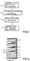
- FIG. 3illustrates an exemplary embodiment of the stack interconnection method according to the invention.
- the first stepmarked 61, consists in electrically connecting the pads P C of the plates P to the lateral faces of the stack. This step is illustrated in FIG. 4, which is a section along the plane AA in FIG. 1.
- a conductive wire Fis connected, for example by welding, to each of the pads P C of each of the wafers.
- Each of the wires Fis directed towards one of the faces of the stack, according to the needs of the connectors.
- the wires Fcan be replaced by conductive tapes.
- each of the plates Pcan be, before stacking, covered with a drop of protective insulating material (silicone or the like), as is customary for the protection of semiconductor pads.
- the assemblyis then joined together using an insulating material D, such as an epoxy resin.
- an insulating material Dsuch as an epoxy resin.
- the dielectric material Dhas not been hatched although seen in section.
- the stackis then cut or polished so that the wires F are flush with the faces of the stack.
- the next step (63, FIG. 3)consists in depositing one (or more) conductive layer M, metallic for example, on all of the faces of the stack thus formed.
- the next step (64, FIG. 3)consists in making connections on the lateral faces of the stack, from layer M, connecting the wires F to each other and to the pads P E.
- FIG. 5represents a stack according to the invention on which are illustrated examples of connections.
- FIGS. 6a and 6billustrate in more detail step 64 of making the connections C.
- FIG. 6arepresents a fractional and enlarged view of a piece of the stack of FIG. 5, where we see a connection C and a stacking pad P E.
- Figure 6bis a sectional view along an axis BB of Figure 6a.
- connection Cis formed by two etchings 51 and 52, produced using a laser which locally destroys the metallic layer M and brings up the insulating layer D (dotted in FIG. 6a for clarity of the diagram), making thus the electrical insulation of connection C from the rest of layer M.
- the stacking pads P Ecan advantageously be produced by the same laser engraving technique, as shown in FIG. 6a.
- the studs P Ewhen they are located in the vicinity of the base, extend a little on the latter so as to facilitate the mounting and the connection of the stack when these are produced on the surface , i.e. without connection pins.
- FIG. 7represents another embodiment of the method according to the invention.
- connection of wires (or ribbons) to the pads P C of the pads P(step 61), stacking and joining of the pads (step 62), are identical to what has been described in FIG. 3.
- the next step (73)consists in making a groove in the stack, at the level where the wires F are flush so as to release the end of the latter.
- This stephas been illustrated in FIG. 8 where an alignment of five wires F of the face F L of FIG. 5 has been reproduced by way of example, the groove being marked 81 and the stack, E.
- These grooves such as 81can be produced by laser engraving in the insulating material D (see FIG. 4).
- the next step (74)consists in depositing a conductive layer (metal for example) over the entire stack, that is to say faces of the stack, grooves (such as 81) and wires F.
- a conductive layermetal for example
- the last step (75) shown in FIG. 7consists in removing the conductive layer on the flat surfaces of the stack, so as to only allow it to remain in the grooves such as 81 where it makes the desired connection.
- This last stepcan be carried out for example by polishing or using a laser.
- FIG. 8shows by way of example a straight groove 81 connecting aligned wires F, but the grooves can of course take any shape and connect any wire F depending on the connections to be made.
- This embodimenthas the advantage, compared to the previous one, of allowing a smaller connection pitch.
- FIG. 9illustrates an alternative embodiment of the connections of the plates on the faces of the stack according to the invention.
- an insulating material 95is deposited in each of the grooves so as to seal them. If necessary, the section of the wires F is then cleaned so as to allow a later electrical connection.
- the next stepconsists in metallizing the entire stack E again and then in etching in this last conductive layer the contours (98) of the connections (96, 97) to be made, in a similar manner to that which is described below. above (step 64 of Figure 3 in conjunction with Figures 6).
- FIG. 9shows only two connections, which have been hatched for the readability of the figure, one (97) connecting one of the wires F of the groove 91 with other non-studs. shown and the other (96) passing through the two grooves (91, 81), without electrical connection.
- This variantthus makes it possible to simply cross connections on the surface of the stack.
- connection pads P E of the platesto the faces of the stack by wires allows these wires to emerge on any face (except the base).
- the wires Fcan be individually insulated.
- the connection to the printed circuitis made by the stacking pads P E which can be placed on any of the faces F V , F R or F L and which, therefore, can be numerous.
- the connection pads P E -Circuit printedare accessible and visible, which reduces the cost and allows certain applications, including military.
- the stackhas been described such that the plates are perpendicular to the printed circuit but that the stack can be produced in the other direction and the plates are parallel to this printed circuit.
- the stacking pads P Ehave been illustrated on the faces F V and F R , but may be arranged on any of the faces of the stack and anywhere on these faces, depending on the application; in fact, when the stack is, as shown in FIG. 1, intended to be placed on a printed circuit, the pads P E can be placed on any face, except the base, but preferably in the vicinity of the edges of the base; but it is also possible to interconnect two (or more) stacks with one another, in which case the studs P E can occupy any position.
- connections C by laserhas been described using an etching technique, but it is also possible to use a deposition technique using a laser; for this purpose, the stack is placed in an organometallic vapor and the area where it is desired to form the connection; the heating causes the decomposition of the vapor and the deposition of the metal at the desired location; the deposition of a local insulating layer is done, as necessary, in a similar manner by adapting the composition of the vapor.
- a single layer of connections Chas been shown on the stack, but it is possible to have several (isolated from one another), for example by the laser deposition technique described above, so for example to allow crossings of connections.
Landscapes
- Engineering & Computer Science (AREA)
- Power Engineering (AREA)
- Microelectronics & Electronic Packaging (AREA)
- Computer Hardware Design (AREA)
- General Physics & Mathematics (AREA)
- Physics & Mathematics (AREA)
- Condensed Matter Physics & Semiconductors (AREA)
- Manufacturing & Machinery (AREA)
- Internal Circuitry In Semiconductor Integrated Circuit Devices (AREA)
- Wire Bonding (AREA)
- Automatic Control Of Machine Tools (AREA)
- Auxiliary Devices For Machine Tools (AREA)
- Turning (AREA)
- Numerical Control (AREA)
- Design And Manufacture Of Integrated Circuits (AREA)
Abstract
Description
Translated fromFrenchLa présente invention a pour objet un procédé et un dispositif pour l'interconnexion de pastilles semi-conductrices empilées, chacune des pastilles contenant un circuit intégré.The present invention relates to a method and a device for the interconnection of stacked semiconductor pads, each of the pads containing an integrated circuit.
Il a déjà été proposé de réaliser des empilements de circuits intégrés, comme par exemple décrit dans le brevet américain n° 4. 706. 166. Selon cette réalisation, les pastilles sont disposées sur un circuit imprimé, accolées les unes aux autres perpendiculairement au circuit imprimé ; les plots de connexion de chacune des pastilles sont ramenés sur un même côté de la pastille ; ce côté est disposé sur le circuit imprimé et les connexions avec ce dernier y sont réalisées. Toutefois, cet arrangement présente notamment des limitations liées au nombre de plots qu'il est matériellement possible de disposer sur un seul côté d'une pastille semi-conductrice ; en outre, il est onéreux du fait que les pastilles ne sont pas standard (la disposition des plots doit être modifiée) ; enfin, les connexions ainsi réalisées sont peu accessibles et de plus non visibles, ce qui en limite l'utilisation.It has already been proposed to make stacks of integrated circuits, as for example described in American patent n ° 4. 706. 166. According to this embodiment, the pads are placed on a printed circuit, placed side by side perpendicular to the circuit. printed; the connection pads of each of the pads are brought to the same side of the pad; this side is arranged on the printed circuit and the connections with the latter are made there. However, this arrangement has in particular limitations linked to the number of pads that it is physically possible to have on one side of a semiconductor chip; in addition, it is expensive because the pads are not standard (the arrangement of the pads must be changed); finally, the connections thus made are not very accessible and moreover not visible, which limits their use.
La présente invention a pour objet un dispositif d'interconnexion de circuits intégrés empilés qui évite ces inconvénients et limitations par l'utilisation des faces de l'empilement comme surface d'interconnexion.The present invention relates to an interconnection device for stacked integrated circuits which avoids these drawbacks and limitations by the use of the faces of the stack as an interconnection surface.
Plus précisément, des plaquettes formées de une ou plusieurs pastilles semi-conductrices sont empilées et rendues solidaires les unes des autres ; dans un mode de réalisation, leurs plots de connexion sont chacun reliés à l'une quelconque des faces de l'empilement sauf une, dite base, qui est destinée à être en contact avec un substrat de circuit imprimé. La connexion des plaquettes entre elles est réalisée sur les faces de l'empilement ; le cas échéant, la connexion des plaquettes avec le circuit imprimé est réalisée par l'intermédiaire de plots dits d'empilement, formés sur les faces de l'empilement, par exemple au voisinage des arêtes de la base, les connexions joignant les plots entre eux étant formées sur les faces de l'empilement et certaines d'entre elles au moins étant non rectilignes.More specifically, wafers formed from one or more semiconductor wafers are stacked and made integral with each other; in one embodiment, their connection pads are each connected to any one of the faces of the stack except one, called base, which is intended to be in contact with a printed circuit substrate. The connection of the wafers to each other is carried out on the faces of the stack; where appropriate, the connection of the wafers with the printed circuit is carried out by means of so-called stacking pads, formed on the faces of the stack, for example in the vicinity of the edges of the base, the connections joining the pads between them being formed on the faces of the stack and at least some of them being non-rectilinear.
D'autres objets, particularités et résultats de l'invention ressortiront de la description suivante, illustrée par les dessins annexés qui représentent :
- la figure 1, une vue en perspective éclatée d'un mode de réalisation de l'empilement de plaquettes semi-conductrices selon l'invention ;
- la figure 2, un exemple de plaquette insérée dans l'empilement de la figure précédente ;
- la figure 3, un premier mode de réalisation du procédé d'interconnexion d'empilement selon l'invention ;
- la figure 4, une vue en coupe fractionnaire d'un mode de réalisation pratique de l'empilement selon l'invention ;
- la figure 5, un mode de réalisation des connexions des plaquettes sur les faces de l'empilement selon l'invention ;
- les figures 6a et 6b, des détails de réalisation de la figure précédente ;
- la figure 7, un autre mode de réalisation du procédé selon l'invention ;
- la figure 8, une vue fractionnaire d'une étape du procédé de la figure précédente ;
- la figure 9, une variante de réalisation des connexions des plaquettes sur les faces de l'empilement selon l'invention.
- Figure 1, an exploded perspective view of an embodiment of the stack of semiconductor wafers according to the invention;
- Figure 2, an example of insert inserted in the stack of the previous figure;
- FIG. 3, a first embodiment of the stack interconnection method according to the invention;
- Figure 4, a fractional sectional view of a practical embodiment of the stack according to the invention;
- FIG. 5, an embodiment of the connections of the plates on the faces of the stack according to the invention;
- Figures 6a and 6b, details of the embodiment of the previous figure;
- Figure 7, another embodiment of the method according to the invention;
- Figure 8, a fractional view of a step in the method of the previous figure;
- Figure 9, an alternative embodiment of the wafer connections on the faces of the stack according to the invention.
Sur ces différentes figures, les mêmes références se rapportent aux mêmes éléments. En outre, pour la clarté des dessins, l'échelle réelle n'est pas respectée.In these different figures, the same references relate to the same elements. In addition, for the sake of clarity of the drawings, the actual scale is not respected.
La figure 1 est donc une vue éclatée d'un empilement selon l'invention de plaquettes semi-conductrices.Figure 1 is therefore an exploded view of a stack according to the invention of semiconductor wafers.
Sur cette figure, on trouve donc une pluralité de plaquettes P (trois plaquettes sur le schéma) disposées parallèlement les unes aux autres. Les plaquettes P peuvent être des pastilles semi-conductrices ou un circuit imprimé, céramique ou époxy, comportant une ou plusieurs puces semi-conductrices. L'empilement est par exemple fermé par une première plaque isolante FV, formant face avant et une deuxième plaque isolante FR, formant face arrière.In this figure, there is therefore a plurality of plates P (three plates on the diagram) arranged parallel to each other. The plates P can be semiconductor wafers or a printed circuit, ceramic or epoxy, comprising one or more semiconductor chips. The stack is for example closed by a first insulating plate FV , forming the front face and a second insulating plate FR , forming the rear face.
La figure 2 représente, à titre d'exemple, une plaquette P de l'empilement de la figure précédente, constituée par une pastille semi-conductrice.FIG. 2 represents, by way of example, a wafer P of the stack of the previous figure, constituted by a semiconductor chip.
Celle-ci se compose d'une plaquette semi-conductrice 20 dans laquelle est réalisé un circuit intégré quelconque, une mémoire par exemple. A la surface de la plaquette P, apparaissent des plots PC, disposés par exemple au voisinage de deux des bords de la plaquette, permettant la connexion électrique du circuit contenu dans la plaquette vers l'extérieur ; les plots PC peuvent bien entendu être disposés autour des quatre côtés de la plaquette P, ou encore en un point quelconque de sa surface.This consists of a
L'empilement de la figure 1 est, dans ce mode de réalisation, destiné à être disposé sur un substrat de circuit imprimé CI par l'intermédiaire de l'une de ses faces B, appelée base. Les faces avant et arrière FV et FR, par exemple, portent des plots PE dits d'empilement, destinés à la connexion de l'empilement vers les autres circuits portés par le circuit imprimé CI. Ces plots d'empilement PE sont disposés par exemple au voisinage de la base B.The stack of FIG. 1 is, in this embodiment, intended to be placed on a printed circuit substrate CI via one of its faces B, called the base. The front and rear faces FV and FR , for example, carry so-called stack pads PE , intended for the connection of the stack to the other circuits carried by the printed circuit CI. These stacking pads PE are arranged for example in the vicinity of the base B.
La figure 3 illustre un exemple de réalisation du procédé d'interconnexion d'empilement selon l'invention.FIG. 3 illustrates an exemplary embodiment of the stack interconnection method according to the invention.
La première étape, repérée 61, consiste à relier électriquement les plots PC des plaquettes P aux faces latérales de l'empilement. Cette étape est illustrée sur la figure 4, qui est une coupe selon le plan A-A de la figure 1.The first step, marked 61, consists in electrically connecting the pads PC of the plates P to the lateral faces of the stack. This step is illustrated in FIG. 4, which is a section along the plane AA in FIG. 1.
Sur la figure 4, on retrouve la face avant FV, la face arrière FR et, entre ces deux faces, trois plaquettes P. Ainsi qu'il est connu, la surface de chacune de ces plaquettes est recouverte d'une couche d'isolant 30, sauf aux endroits des plots de connexion PC.In FIG. 4, we find the front face FV , the rear face FR and, between these two faces, three plates P. As is known, the surface of each of these plates is covered with a layer d insulation 30, except at the locations of the connection pads PC.
Selon l'invention, on connecte un fil conducteur F, par exemple par soudure, sur chacun des plots PC de chacune des plaquettes. Chacun des fils F est dirigé vers l'une des faces de l'empilement, selon les besoins de la connectique. Sur la figure 4 on a, à titre d'exemple, dirigé les fils F représentés vers la même face. Dans une variante de réalisation, les fils F peuvent être remplacés par des rubans conducteurs. Pour simplifier la description, on parlera ci-après uniquement de "fils conducteurs" ou de "conducteurs" F.According to the invention, a conductive wire F is connected, for example by welding, to each of the pads PC of each of the wafers. Each of the wires F is directed towards one of the faces of the stack, according to the needs of the connectors. In Figure 4 we have, by way of example, directed the son F shown to the same face. In an alternative embodiment, the wires F can be replaced by conductive tapes. To simplify the description, we will speak hereinafter only of "conductive wires" or of "conductors" F.
Lors de l'étape suivante (62, figure 3 ), on réalise l'empilement des plaquettes P. Dans une variante de réalisation, chacune des plaquettes P peut être, avant empilement, recouverte d'une goutte de matériau isolant de protection (silicone ou analogue), comme il est usuel pour la protection des pastilles semi-conductrices. On procède alors à la solidarisation de l'ensemble à l'aide d'un matériau isolant D, tel qu'une résine époxy. Pour la clarté de la figure 4, le matériau diélectrique D n'a pas été hachuré bien que vu en coupe. L'empilement est alors découpé ou poli de sorte que les fils F affleurent sur les faces de l'empilement.During the next step (62, FIG. 3), the plates P are stacked. In an alternative embodiment, each of the plates P can be, before stacking, covered with a drop of protective insulating material (silicone or the like), as is customary for the protection of semiconductor pads. The assembly is then joined together using an insulating material D, such as an epoxy resin. For the clarity of FIG. 4, the dielectric material D has not been hatched although seen in section. The stack is then cut or polished so that the wires F are flush with the faces of the stack.
L'étape suivante (63, figure 3) consiste à déposer une ( ou plusieurs ) couche M conductrice, métallique par exemple, sur l'ensemble des faces de l'empilement ainsi constitué.The next step (63, FIG. 3) consists in depositing one (or more) conductive layer M, metallic for example, on all of the faces of the stack thus formed.
L'étape suivante (64, figure 3) consiste à réaliser sur les faces latérales de l'empilement, à partir de la couche M, des connexions reliant les fils F entre eux et aux plots PE.The next step (64, FIG. 3) consists in making connections on the lateral faces of the stack, from layer M, connecting the wires F to each other and to the pads PE.
La figure 5 représente un empilement selon l'invention sur lequel sont illustrés des exemples de connexions.FIG. 5 represents a stack according to the invention on which are illustrated examples of connections.
Sur cette figure, on retrouve l'empilement comportant la face avant FV, la base B, la face opposée à la base (face supérieure) étant repérée FS et les deux faces restantes FL étant dites faces latérales . On voit les fils F affleurer sur une face latérale FL. Ils sont à la fois interconnectés entre eux et reliés à des plots d'empilement PE à l'aide de connexions C. On a représenté également, toujours à titre d'exemple, certains fils F affleurant sur la face supérieure FD de l'empilement et reliés chacun à un plot d'empilement PE distinct par une connexion C. A titre d'exemple encore, on a illustré des plots PE sur la face FV au voisinage de la base, mais il est entendu qu'ils peuvent occuper toute position sur les faces de l'empilement, sauf sur la base B.In this figure, we find the stack comprising the front face FV , the base B, the face opposite to the base (upper face) being marked FS and the two remaining faces FL being called lateral faces. We see the wires F flush on a lateral face FL. They are both interconnected with one another and connected to stacking studs PE by means of connections C. Also shown, still by way of example, certain wires F which are flush with the upper face FD of l stack and each connected to a separate stack pad PE by a connection C. As another example, pads PE have been illustrated on the face FV in the vicinity of the base, but it is understood that they can occupy any position on the faces of the stack, except on base B.
Les figures 6a et 6b illustrent plus en détail l'étape 64 de réalisation des connexions C.FIGS. 6a and 6b illustrate in
La figure 6a représente une vue fractionnaire et agrandie d'un morceau de l'empilement de la figure 5, où l'on voit une connexion C et un plot d'empilement PE. La figure 6b est une vue en coupe selon un axe BB de la figure 6a.FIG. 6a represents a fractional and enlarged view of a piece of the stack of FIG. 5, where we see a connection C and a stacking pad PE. Figure 6b is a sectional view along an axis BB of Figure 6a.
Chacune des connexions C est formée par deux gravures 51 et 52, réalisées à l'aide d'un laser qui détruit localement la couche métallique M et fait apparaître la couche isolante D (pointillée sur la figure 6a pour la clarté du schéma), réalisant ainsi l'isolation électrique de la connexion C du reste de la couche M.Each of the connections C is formed by two
Les plots d'empilement PE peuvent être avantageusement réalisés par la même technique de gravure laser, comme représenté sur la figure 6a.The stacking pads PE can advantageously be produced by the same laser engraving technique, as shown in FIG. 6a.
Dans une variante de réalisation, les plots PE, lorsqu'ils sont situés au voisinage de la base, se prolongent un peu sur cette dernière de façon à faciliter le montage et la connexion de l'empilement lorsque ceux-ci sont réalisés en surface, c'est-à-dire sans broches de connexion.In an alternative embodiment, the studs PE , when they are located in the vicinity of the base, extend a little on the latter so as to facilitate the mounting and the connection of the stack when these are produced on the surface , i.e. without connection pins.
La figure 7 représente un autre mode de réalisation du procédé selon l'invention.FIG. 7 represents another embodiment of the method according to the invention.
Les deux premières étapes du procédé, à savoir connexion de fils (ou rubans) sur les plots PC des plaquettes P (étape 61), empilement et solidarisation des plaquettes (étape 62), sont identiques à ce qui a été décrit figure 3.The first two stages of the process, namely connection of wires (or ribbons) to the pads PC of the pads P (step 61), stacking and joining of the pads (step 62), are identical to what has been described in FIG. 3.
L'étape suivante (73) consiste, à réaliser une rainure dans l'empilement, au niveau où les fils F affleurent de sorte à dégager l'extrémité de ces derniers. Cette étape a été illustrée sur la figure 8 où on a reproduit à titre d'exemple un alignement de cinq fils F de la face FL de la figure 5, la rainure étant repérée 81 et l'empilement, E. Ces rainures telles que 81 peuvent être réalisées par gravure laser dans le matériau isolant D ( voir figure 4 ).The next step (73) consists in making a groove in the stack, at the level where the wires F are flush so as to release the end of the latter. This step has been illustrated in FIG. 8 where an alignment of five wires F of the face FL of FIG. 5 has been reproduced by way of example, the groove being marked 81 and the stack, E. These grooves such as 81 can be produced by laser engraving in the insulating material D (see FIG. 4).
L'étape suivante (74) consiste à déposer une couche conductrice (métal par exemple) sur la totalité de l'empilement, c'est-à-dire faces de l'empilement, rainures (telles que 81) et fils F.The next step (74) consists in depositing a conductive layer (metal for example) over the entire stack, that is to say faces of the stack, grooves (such as 81) and wires F.
Enfin, la dernière étape (75) représentée figure 7 consiste à enlever la couche conductrice sur les surfaces planes de l'empilement, de sorte à ne la laisser subsister que dans les rainures telles que 81 où elle réalise la connexion recherchée. Cette dernière étape peut être réalisée par exemple par polissage ou à l'aide d'un laser.Finally, the last step (75) shown in FIG. 7 consists in removing the conductive layer on the flat surfaces of the stack, so as to only allow it to remain in the grooves such as 81 where it makes the desired connection. This last step can be carried out for example by polishing or using a laser.
On a représenté à titre d'exemple sur la figure 8 une rainure 81 droite reliant des fils F alignés, mais les rainures peuvent bien entendu affecter toute forme et relier tout fil F en fonction des connexions à réaliser.FIG. 8 shows by way of example a
Ce mode de réalisation a l'avantage, par rapport au précédent, de permettre un pas de connexion plus petit.This embodiment has the advantage, compared to the previous one, of allowing a smaller connection pitch.
La figure 9 illustre une variante de réalisation des connexions des plaquettes sur les faces de l'empilement selon l'invention.FIG. 9 illustrates an alternative embodiment of the connections of the plates on the faces of the stack according to the invention.
Sur cette figure, on a représenté l'empilement E tel qu'obtenu après le procédé décrit figure 7, c'est-à-dire présentant des rainures (81, 91) formées au niveau des fils F, les rainures et les fils F étant métallisés (couches 92 et 93, respectivement) et les faces planes FL de l'empilement étant dé-métallisées.In this figure, there is shown the stack E as obtained after the process described in Figure 7, that is to say having grooves (81, 91) formed at the son F, the grooves and son F being metallized (
Selon cette variante, on procède au dépôt d'un matériau isolant 95 dans chacune des rainures de sorte à les colmater. Si nécessaire, on nettoie ensuite la section des fils F de façon à permettre une connexion électrique ultérieure.According to this variant, an insulating
L'étape suivante consiste à métalliser à nouveau l'ensemble de l'empilement E puis à graver dans cette dernière couche conductrice les contours (98) des connexions (96, 97) à réaliser, de façon analogue à ce qui est décrit ci-dessus (étape 64 de la figure 3 en liaison avec les figures 6).The next step consists in metallizing the entire stack E again and then in etching in this last conductive layer the contours (98) of the connections (96, 97) to be made, in a similar manner to that which is described below. above (step 64 of Figure 3 in conjunction with Figures 6).
A titre d'exemple, on a représenté figure 9 deux connexions seulement, qu'on a hachuré pour la lisibilité de la figure, l'une (97) connectant l'un des fils F de la rainure 91 avec d'autres plots non représentés et l'autre (96) traversant les deux rainures ( 91, 81 ), sans connexion électrique.By way of example, FIG. 9 shows only two connections, which have been hatched for the readability of the figure, one (97) connecting one of the wires F of the
Cette variante permet ainsi de réaliser simplement des croisements de connexions à la surface de l'empilement.This variant thus makes it possible to simply cross connections on the surface of the stack.
Il apparaît qu'on a ainsi réalisé un empilement de plaquettes contenant des circuits intégrés qui peuvent être identiques entre eux ou non, tant sur le plan électrique que sur le plan de la géométrie de la plaquette. Ces plaquettes sont interconnectées entre elles par les faces de l'empilement, sans nécessiter de passage par le circuit imprimé, ce qui permet de diminuer le nombre de plots d'empilement PE ou, inversement, d'augmenter le nombre ou la complexité des plaquettes empilables.It appears that a stack of wafers has thus been produced containing integrated circuits which may or may not be identical to each other, both electrically and in terms of the geometry of the wafer. These plates are interconnected with each other by the faces of the stack, without requiring passage through the printed circuit, which allows reduce the number of stacking pads PE or, conversely, increase the number or complexity of stackable wafers.
Egalement, le fait de relier les plots PC des plaquettes aux faces de l'empilement par des fils permet de faire émerger ces fils sur n'importe quelle face (hors la base). Dans une variante de réalisation, les fils F peuvent être individuellement isolés. De plus, la connexion au circuit imprimé se fait par les plots d'empilement PE qui peuvent être placés sur n'importe laquelle des faces FV, FR ou FL et qui, de ce fait, peuvent être nombreux. Enfin, les connexions plots PE-circuit imprimé sont accessibles et visibles, ce qui en diminue le coût et autorise certaines applications, militaires notamment.Also, the fact of connecting the pads PC of the plates to the faces of the stack by wires allows these wires to emerge on any face (except the base). In an alternative embodiment, the wires F can be individually insulated. In addition, the connection to the printed circuit is made by the stacking pads PE which can be placed on any of the faces FV , FR or FL and which, therefore, can be numerous. Finally, the connection pads PE -Circuit printed are accessible and visible, which reduces the cost and allows certain applications, including military.
La description faite ci-dessus l'a été bien entendu à titre d'exemple non limitatif. C'est ainsi par exemple que l'empilement a été décrit tel que les plaquettes soient perpendiculaires au circuit imprimé mais que l'empilement peut être réalisé dans l'autre direction et les plaquettes être parallèles à ce circuit imprimé. Egalement, les plots d'empilement PE ont été illustrés sur les faces FV et FR, mais peuvent être disposés sur n'importe laquelle des faces de l'empilement et n'importe où sur ces faces, selon l'application ; en effet, lorsque l'empilement est, comme représenté figure 1, destiné à être disposé sur un circuit imprimé, on peut disposer les plots PE sur n'importe quelle face, sauf la base, mais de préférence au voisinage des arêtes de la base ; mais il est également possible d'interconnecter deux (ou plus) empilements entre eux, auquel cas les plots PE peuvent occuper n'importe quelle position. De la même manière, on a décrit un procédé de réalisation des connexions C par laser utilisant une technique de gravure mais on peut utiliser également une technique de dépôt à l'aide d'un laser ; à cet effet, on place l'empilement dans une vapeur organométallique et on chauffe à l'aide du laser la zone où on désire former la connexion ; l'échauffement provoque la décomposition de la vapeur et le dépôt du métal à l'endroit voulu ; le dépôt d'une couche isolante locale se fait, en tant que besoin, de façon analogue en adaptant la composition de la vapeur. Enfin, on a représenté une seule couche de connexions C sur l'empilement, mais on peut en disposer plusieurs (isolées entre elles), par exemple par la technique du dépôt laser décrite ci-dessus, de sorte par exemple à permettre les croisements de connexions.The description given above has been understood by way of non-limiting example. Thus, for example, the stack has been described such that the plates are perpendicular to the printed circuit but that the stack can be produced in the other direction and the plates are parallel to this printed circuit. Also, the stacking pads PE have been illustrated on the faces FV and FR , but may be arranged on any of the faces of the stack and anywhere on these faces, depending on the application; in fact, when the stack is, as shown in FIG. 1, intended to be placed on a printed circuit, the pads PE can be placed on any face, except the base, but preferably in the vicinity of the edges of the base; but it is also possible to interconnect two (or more) stacks with one another, in which case the studs PE can occupy any position. Likewise, a method of making connections C by laser has been described using an etching technique, but it is also possible to use a deposition technique using a laser; for this purpose, the stack is placed in an organometallic vapor and the area where it is desired to form the connection; the heating causes the decomposition of the vapor and the deposition of the metal at the desired location; the deposition of a local insulating layer is done, as necessary, in a similar manner by adapting the composition of the vapor. Finally, a single layer of connections C has been shown on the stack, but it is possible to have several (isolated from one another), for example by the laser deposition technique described above, so for example to allow crossings of connections.
Claims (12)
Translated fromFrenchApplications Claiming Priority (2)
| Application Number | Priority Date | Filing Date | Title |
|---|---|---|---|
| FR9015473AFR2670323B1 (en) | 1990-12-11 | 1990-12-11 | METHOD AND DEVICE FOR INTERCONNECTING THREE-DIMENSIONAL INTEGRATED CIRCUITS. |
| FR9015473 | 1990-12-11 |
Publications (2)
| Publication Number | Publication Date |
|---|---|
| EP0490739A1true EP0490739A1 (en) | 1992-06-17 |
| EP0490739B1 EP0490739B1 (en) | 1997-06-18 |
Family
ID=9403101
Family Applications (1)
| Application Number | Title | Priority Date | Filing Date |
|---|---|---|---|
| EP91403307AExpired - LifetimeEP0490739B1 (en) | 1990-12-11 | 1991-12-06 | Interconnection method and device for three-dimensional integrated circuits |
Country Status (7)
| Country | Link |
|---|---|
| EP (1) | EP0490739B1 (en) |
| JP (1) | JP3415621B2 (en) |
| KR (1) | KR920704344A (en) |
| DE (1) | DE69126599T2 (en) |
| ES (1) | ES2104681T3 (en) |
| FR (1) | FR2670323B1 (en) |
| WO (1) | WO1992010853A1 (en) |
Cited By (25)
| Publication number | Priority date | Publication date | Assignee | Title |
|---|---|---|---|---|
| WO1993018549A1 (en)* | 1992-03-13 | 1993-09-16 | Thomson-Csf | Process and device for three-dimensional interconnection of housings for electronic components |
| FR2688629A1 (en)* | 1992-03-10 | 1993-09-17 | Thomson Csf | Method and device for three-dimensional encapsulation of semiconductor chips |
| US5455455A (en)* | 1992-09-14 | 1995-10-03 | Badehi; Peirre | Methods for producing packaged integrated circuit devices and packaged integrated circuit devices produced thereby |
| EP0766909A4 (en)* | 1994-06-23 | 1997-10-22 | Cubic Memory | VERTICAL INTERCONNECTION PROCESS FOR SILICON SEGMENTS |
| US5716759A (en)* | 1993-09-02 | 1998-02-10 | Shellcase Ltd. | Method and apparatus for producing integrated circuit devices |
| US5847448A (en)* | 1990-12-11 | 1998-12-08 | Thomson-Csf | Method and device for interconnecting integrated circuits in three dimensions |
| EP0593330B1 (en)* | 1992-10-13 | 1998-12-09 | Thomson-Csf | 3D-interconnection method for electronic component housings and resulting 3D component |
| US5891761A (en)* | 1994-06-23 | 1999-04-06 | Cubic Memory, Inc. | Method for forming vertical interconnect process for silicon segments with thermally conductive epoxy preform |
| US6040235A (en)* | 1994-01-17 | 2000-03-21 | Shellcase Ltd. | Methods and apparatus for producing integrated circuit devices |
| US6080596A (en)* | 1994-06-23 | 2000-06-27 | Cubic Memory Inc. | Method for forming vertical interconnect process for silicon segments with dielectric isolation |
| US6117707A (en)* | 1994-07-13 | 2000-09-12 | Shellcase Ltd. | Methods of producing integrated circuit devices |
| US6124633A (en)* | 1994-06-23 | 2000-09-26 | Cubic Memory | Vertical interconnect process for silicon segments with thermally conductive epoxy preform |
| WO2001045172A1 (en)* | 1999-12-15 | 2001-06-21 | 3D Plus | Method and device for interconnecting electronic components in three dimensions |
| US6255726B1 (en) | 1994-06-23 | 2001-07-03 | Cubic Memory, Inc. | Vertical interconnect process for silicon segments with dielectric isolation |
| US6486528B1 (en) | 1994-06-23 | 2002-11-26 | Vertical Circuits, Inc. | Silicon segment programming apparatus and three terminal fuse configuration |
| US6624505B2 (en) | 1998-02-06 | 2003-09-23 | Shellcase, Ltd. | Packaged integrated circuits and methods of producing thereof |
| US7033664B2 (en) | 2002-10-22 | 2006-04-25 | Tessera Technologies Hungary Kft | Methods for producing packaged integrated circuit devices and packaged integrated circuit devices produced thereby |
| US7408249B2 (en) | 1998-02-06 | 2008-08-05 | Tessera Technologies Hungary Kft. | Packaged integrated circuits and methods of producing thereof |
| RU2336595C2 (en)* | 2006-09-01 | 2008-10-20 | Александр Иванович Завадский | Method of spatial mini module manufacturing for radio electronic devices |
| US7566853B2 (en) | 2005-08-12 | 2009-07-28 | Tessera, Inc. | Image sensor employing a plurality of photodetector arrays and/or rear-illuminated architecture |
| EP2202789A1 (en)* | 2008-12-24 | 2010-06-30 | Nxp B.V. | Stack of molded integrated circuit dies with side surface contact tracks |
| US7781240B2 (en) | 1998-02-06 | 2010-08-24 | Tessera Technologies Hungary Kft. | Integrated circuit device |
| RU2460171C2 (en)* | 2010-08-23 | 2012-08-27 | Федеральное государственное унитарное предприятие Омский научно-исследовательский институт приборостроения (ФГУП ОНИИП) | Volume module for radio electronics equipment |
| US8359740B2 (en) | 2008-12-19 | 2013-01-29 | 3D Plus | Process for the wafer-scale fabrication of electronic modules for surface mounting |
| US8461542B2 (en) | 2008-09-08 | 2013-06-11 | Koninklijke Philips Electronics N.V. | Radiation detector with a stack of converter plates and interconnect layers |
Families Citing this family (3)
| Publication number | Priority date | Publication date | Assignee | Title |
|---|---|---|---|---|
| FR2785452B1 (en)* | 1998-11-03 | 2003-06-13 | Tda Armements Sas | METHOD FOR PRODUCING RADIO WAVES RECEIVERS BY INTERCONNECTION OF THREE-DIMENSIONAL INTEGRATED CIRCUITS |
| JP5264640B2 (en)* | 2009-07-24 | 2013-08-14 | 新光電気工業株式会社 | Multilayer semiconductor device and manufacturing method thereof |
| DE102016104626A1 (en) | 2015-03-16 | 2016-09-22 | Jtekt Corporation | spindle device |
Citations (3)
| Publication number | Priority date | Publication date | Assignee | Title |
|---|---|---|---|---|
| US3746934A (en)* | 1971-05-06 | 1973-07-17 | Siemens Ag | Stack arrangement of semiconductor chips |
| EP0019186A1 (en)* | 1979-05-17 | 1980-11-26 | Siemens Aktiengesellschaft | Joining the connection wires of semiconductor systems to the carrier elements |
| FR2645681A1 (en)* | 1989-04-07 | 1990-10-12 | Thomson Csf | Vertical interconnection device for integrated-circuit chips and its method of manufacture |
- 1990
- 1990-12-11FRFR9015473Apatent/FR2670323B1/ennot_activeExpired - Fee Related
- 1991
- 1991-12-06WOPCT/FR1991/000978patent/WO1992010853A1/enunknown
- 1991-12-06JPJP50211392Apatent/JP3415621B2/ennot_activeExpired - Lifetime
- 1991-12-06DEDE69126599Tpatent/DE69126599T2/ennot_activeExpired - Lifetime
- 1991-12-06KRKR1019920701892Apatent/KR920704344A/ennot_activeAbandoned
- 1991-12-06ESES91403307Tpatent/ES2104681T3/ennot_activeExpired - Lifetime
- 1991-12-06EPEP91403307Apatent/EP0490739B1/ennot_activeExpired - Lifetime
Patent Citations (3)
| Publication number | Priority date | Publication date | Assignee | Title |
|---|---|---|---|---|
| US3746934A (en)* | 1971-05-06 | 1973-07-17 | Siemens Ag | Stack arrangement of semiconductor chips |
| EP0019186A1 (en)* | 1979-05-17 | 1980-11-26 | Siemens Aktiengesellschaft | Joining the connection wires of semiconductor systems to the carrier elements |
| FR2645681A1 (en)* | 1989-04-07 | 1990-10-12 | Thomson Csf | Vertical interconnection device for integrated-circuit chips and its method of manufacture |
Cited By (36)
| Publication number | Priority date | Publication date | Assignee | Title |
|---|---|---|---|---|
| US5847448A (en)* | 1990-12-11 | 1998-12-08 | Thomson-Csf | Method and device for interconnecting integrated circuits in three dimensions |
| FR2688629A1 (en)* | 1992-03-10 | 1993-09-17 | Thomson Csf | Method and device for three-dimensional encapsulation of semiconductor chips |
| EP0565391A1 (en)* | 1992-03-10 | 1993-10-13 | Thomson-Csf | Method and device for encapsulation of three-dimensional semi-conductor chips |
| US5400218A (en)* | 1992-03-10 | 1995-03-21 | Thomson-Csf | Device for the 3D encapsulation of semiconductor chips |
| FR2688630A1 (en)* | 1992-03-13 | 1993-09-17 | Thomson Csf | METHOD AND DEVICE FOR THREE-DIMENSIONAL INTERCONNECTION OF ELECTRONIC COMPONENT PACKAGES. |
| WO1993018549A1 (en)* | 1992-03-13 | 1993-09-16 | Thomson-Csf | Process and device for three-dimensional interconnection of housings for electronic components |
| US5885850A (en)* | 1992-03-13 | 1999-03-23 | Thomson-Csf | Method for the 3D interconnection of packages of electronic components, and device obtained by this method |
| EP0660967B1 (en)* | 1992-09-14 | 2001-04-11 | Shellcase Ltd. | Method for producing integrated circuit devices |
| US5455455A (en)* | 1992-09-14 | 1995-10-03 | Badehi; Peirre | Methods for producing packaged integrated circuit devices and packaged integrated circuit devices produced thereby |
| EP0593330B1 (en)* | 1992-10-13 | 1998-12-09 | Thomson-Csf | 3D-interconnection method for electronic component housings and resulting 3D component |
| US5716759A (en)* | 1993-09-02 | 1998-02-10 | Shellcase Ltd. | Method and apparatus for producing integrated circuit devices |
| US6040235A (en)* | 1994-01-17 | 2000-03-21 | Shellcase Ltd. | Methods and apparatus for producing integrated circuit devices |
| US6080596A (en)* | 1994-06-23 | 2000-06-27 | Cubic Memory Inc. | Method for forming vertical interconnect process for silicon segments with dielectric isolation |
| US5891761A (en)* | 1994-06-23 | 1999-04-06 | Cubic Memory, Inc. | Method for forming vertical interconnect process for silicon segments with thermally conductive epoxy preform |
| US6255726B1 (en) | 1994-06-23 | 2001-07-03 | Cubic Memory, Inc. | Vertical interconnect process for silicon segments with dielectric isolation |
| US5837566A (en)* | 1994-06-23 | 1998-11-17 | Cubic Memory, Inc. | Vertical interconnect process for silicon segments |
| US6124633A (en)* | 1994-06-23 | 2000-09-26 | Cubic Memory | Vertical interconnect process for silicon segments with thermally conductive epoxy preform |
| US6188126B1 (en) | 1994-06-23 | 2001-02-13 | Cubic Memory Inc. | Vertical interconnect process for silicon segments |
| EP0766909A4 (en)* | 1994-06-23 | 1997-10-22 | Cubic Memory | VERTICAL INTERCONNECTION PROCESS FOR SILICON SEGMENTS |
| US6486528B1 (en) | 1994-06-23 | 2002-11-26 | Vertical Circuits, Inc. | Silicon segment programming apparatus and three terminal fuse configuration |
| EP1158570A1 (en)* | 1994-06-23 | 2001-11-28 | Cubic Memory | Vertical interconnect process for silicon segments |
| US6117707A (en)* | 1994-07-13 | 2000-09-12 | Shellcase Ltd. | Methods of producing integrated circuit devices |
| US7781240B2 (en) | 1998-02-06 | 2010-08-24 | Tessera Technologies Hungary Kft. | Integrated circuit device |
| US6624505B2 (en) | 1998-02-06 | 2003-09-23 | Shellcase, Ltd. | Packaged integrated circuits and methods of producing thereof |
| US7408249B2 (en) | 1998-02-06 | 2008-08-05 | Tessera Technologies Hungary Kft. | Packaged integrated circuits and methods of producing thereof |
| WO2001045172A1 (en)* | 1999-12-15 | 2001-06-21 | 3D Plus | Method and device for interconnecting electronic components in three dimensions |
| US6809367B2 (en) | 1999-12-15 | 2004-10-26 | 3D Plus | Device for interconnecting, in three dimensions, electronic components |
| FR2802706A1 (en)* | 1999-12-15 | 2001-06-22 | 3D Plus Sa | METHOD AND DEVICE FOR THREE-DIMENSIONAL INTERCONNECTION OF ELECTRONIC COMPONENTS |
| EP2136401A1 (en)* | 1999-12-15 | 2009-12-23 | 3D Plus | Process and apparatus for tri-dimensional interconnection of electronic devices |
| US7033664B2 (en) | 2002-10-22 | 2006-04-25 | Tessera Technologies Hungary Kft | Methods for producing packaged integrated circuit devices and packaged integrated circuit devices produced thereby |
| US7566853B2 (en) | 2005-08-12 | 2009-07-28 | Tessera, Inc. | Image sensor employing a plurality of photodetector arrays and/or rear-illuminated architecture |
| RU2336595C2 (en)* | 2006-09-01 | 2008-10-20 | Александр Иванович Завадский | Method of spatial mini module manufacturing for radio electronic devices |
| US8461542B2 (en) | 2008-09-08 | 2013-06-11 | Koninklijke Philips Electronics N.V. | Radiation detector with a stack of converter plates and interconnect layers |
| US8359740B2 (en) | 2008-12-19 | 2013-01-29 | 3D Plus | Process for the wafer-scale fabrication of electronic modules for surface mounting |
| EP2202789A1 (en)* | 2008-12-24 | 2010-06-30 | Nxp B.V. | Stack of molded integrated circuit dies with side surface contact tracks |
| RU2460171C2 (en)* | 2010-08-23 | 2012-08-27 | Федеральное государственное унитарное предприятие Омский научно-исследовательский институт приборостроения (ФГУП ОНИИП) | Volume module for radio electronics equipment |
Also Published As
| Publication number | Publication date |
|---|---|
| DE69126599T2 (en) | 1997-10-02 |
| JPH05505067A (en) | 1993-07-29 |
| KR920704344A (en) | 1992-12-19 |
| WO1992010853A1 (en) | 1992-06-25 |
| EP0490739B1 (en) | 1997-06-18 |
| JP3415621B2 (en) | 2003-06-09 |
| FR2670323B1 (en) | 1997-12-12 |
| FR2670323A1 (en) | 1992-06-12 |
| ES2104681T3 (en) | 1997-10-16 |
| DE69126599D1 (en) | 1997-07-24 |
Similar Documents
| Publication | Publication Date | Title |
|---|---|---|
| EP0490739B1 (en) | Interconnection method and device for three-dimensional integrated circuits | |
| EP0565391B1 (en) | Method and device for encapsulation of three-dimensional semi-conductor chips | |
| EP0638933B1 (en) | Interconnection process of stacked semi-conductors chips and devices | |
| EP0584349B1 (en) | Process and device for three-dimensional interconnection of housings for electronic components | |
| EP0228953B1 (en) | Encapsulation housing for an electronic circuit | |
| EP0593330B1 (en) | 3D-interconnection method for electronic component housings and resulting 3D component | |
| EP0583201B1 (en) | Three-dimensional multichip module | |
| EP0923130B1 (en) | Electronic circuit, in particular for implantable active medical device, like a heart stimulator or defibrillator, and its manufacturing method | |
| FR2495377A1 (en) | ENCAPSULATION FOR AN INTEGRATED CIRCUIT | |
| EP0682365A1 (en) | Three-dimensional interconnection of electronic component housings using printed circuits | |
| EP0310463A1 (en) | Housing for a high-density integrated circuit | |
| EP0647357A1 (en) | Semiconductor chip encapsulation method, device produced by this method and its application to three dimensional chip interconnection | |
| EP0133125A1 (en) | Electronic component housing with a capacitor | |
| EP0254640A1 (en) | Realization method of an electronic memory card and card obtained by this method | |
| FR2645681A1 (en) | Vertical interconnection device for integrated-circuit chips and its method of manufacture | |
| EP1312116A1 (en) | Method for distributed shielding and/or bypass for electronic device with three-dimensional interconnection | |
| FR2572849A1 (en) | High-density monolithic module containing interconnected electronic components and its method of manufacture. | |
| EP0321327B1 (en) | Method of mounting an electronic component and its electronic connections on a support | |
| FR2635920A1 (en) | METHOD FOR MANUFACTURING A CONNECTION ZONE FOR A TRIPLATE-TYPE MICROWAVE CIRCUIT AND CIRCUIT THUS OBTAINED | |
| FR2476389A1 (en) | ELECTRONIC CIRCUIT BOX WITH ALIGNED AND OVERLAY SEMICONDUCTOR PELLETS | |
| WO2003081669A1 (en) | Integrated circuit module and method for making same | |
| EP1054446B1 (en) | Method of packaging semiconductor chip | |
| FR3147043A1 (en) | Method of manufacturing a plurality of electronic components | |
| FR2554964A1 (en) | DECOUPLING CAPACITOR AND MANUFACTURING METHOD THEREOF | |
| WO2000077730A1 (en) | Electronic device comprising a chip fixed on a support and method for making same |
Legal Events
| Date | Code | Title | Description |
|---|---|---|---|
| PUAI | Public reference made under article 153(3) epc to a published international application that has entered the european phase | Free format text:ORIGINAL CODE: 0009012 | |
| AK | Designated contracting states | Kind code of ref document:A1 Designated state(s):DE ES FR GB IT SE | |
| 17P | Request for examination filed | Effective date:19921125 | |
| RAP1 | Party data changed (applicant data changed or rights of an application transferred) | Owner name:THOMSON-CSF | |
| 17Q | First examination report despatched | Effective date:19941104 | |
| GRAG | Despatch of communication of intention to grant | Free format text:ORIGINAL CODE: EPIDOS AGRA | |
| GRAH | Despatch of communication of intention to grant a patent | Free format text:ORIGINAL CODE: EPIDOS IGRA | |
| GRAH | Despatch of communication of intention to grant a patent | Free format text:ORIGINAL CODE: EPIDOS IGRA | |
| GRAA | (expected) grant | Free format text:ORIGINAL CODE: 0009210 | |
| AK | Designated contracting states | Kind code of ref document:B1 Designated state(s):DE ES FR GB IT SE | |
| REF | Corresponds to: | Ref document number:69126599 Country of ref document:DE Date of ref document:19970724 | |
| GBT | Gb: translation of ep patent filed (gb section 77(6)(a)/1977) | Effective date:19970724 | |
| REG | Reference to a national code | Ref country code:ES Ref legal event code:FG2A Ref document number:2104681 Country of ref document:ES Kind code of ref document:T3 | |
| PGFP | Annual fee paid to national office [announced via postgrant information from national office to epo] | Ref country code:SE Payment date:19971117 Year of fee payment:7 | |
| PGFP | Annual fee paid to national office [announced via postgrant information from national office to epo] | Ref country code:ES Payment date:19971222 Year of fee payment:7 | |
| PLBE | No opposition filed within time limit | Free format text:ORIGINAL CODE: 0009261 | |
| STAA | Information on the status of an ep patent application or granted ep patent | Free format text:STATUS: NO OPPOSITION FILED WITHIN TIME LIMIT | |
| 26N | No opposition filed | ||
| PG25 | Lapsed in a contracting state [announced via postgrant information from national office to epo] | Ref country code:SE Free format text:LAPSE BECAUSE OF NON-PAYMENT OF DUE FEES Effective date:19981207 Ref country code:ES Free format text:LAPSE BECAUSE OF EXPIRATION OF PROTECTION Effective date:19981207 | |
| REG | Reference to a national code | Ref country code:ES Ref legal event code:FD2A Effective date:20010301 | |
| REG | Reference to a national code | Ref country code:GB Ref legal event code:IF02 | |
| REG | Reference to a national code | Ref country code:FR Ref legal event code:TP | |
| REG | Reference to a national code | Ref country code:FR Ref legal event code:CD | |
| PGFP | Annual fee paid to national office [announced via postgrant information from national office to epo] | Ref country code:FR Payment date:20101224 Year of fee payment:20 | |
| PGFP | Annual fee paid to national office [announced via postgrant information from national office to epo] | Ref country code:GB Payment date:20101201 Year of fee payment:20 Ref country code:IT Payment date:20101218 Year of fee payment:20 | |
| PGFP | Annual fee paid to national office [announced via postgrant information from national office to epo] | Ref country code:DE Payment date:20101130 Year of fee payment:20 | |
| REG | Reference to a national code | Ref country code:DE Ref legal event code:R071 Ref document number:69126599 Country of ref document:DE | |
| REG | Reference to a national code | Ref country code:DE Ref legal event code:R071 Ref document number:69126599 Country of ref document:DE | |
| REG | Reference to a national code | Ref country code:GB Ref legal event code:PE20 Expiry date:20111205 | |
| PG25 | Lapsed in a contracting state [announced via postgrant information from national office to epo] | Ref country code:GB Free format text:LAPSE BECAUSE OF EXPIRATION OF PROTECTION Effective date:20111205 | |
| PG25 | Lapsed in a contracting state [announced via postgrant information from national office to epo] | Ref country code:DE Free format text:LAPSE BECAUSE OF EXPIRATION OF PROTECTION Effective date:20111207 |