EP0476159A1 - Programmable neural logic device - Google Patents
Programmable neural logic deviceDownload PDFInfo
- Publication number
- EP0476159A1 EP0476159A1EP90117818AEP90117818AEP0476159A1EP 0476159 A1EP0476159 A1EP 0476159A1EP 90117818 AEP90117818 AEP 90117818AEP 90117818 AEP90117818 AEP 90117818AEP 0476159 A1EP0476159 A1EP 0476159A1
- Authority
- EP
- European Patent Office
- Prior art keywords
- cell
- programmable logic
- input
- inputs
- master
- Prior art date
- Legal status (The legal status is an assumption and is not a legal conclusion. Google has not performed a legal analysis and makes no representation as to the accuracy of the status listed.)
- Granted
Links
Images


Classifications
- H—ELECTRICITY
- H03—ELECTRONIC CIRCUITRY
- H03K—PULSE TECHNIQUE
- H03K19/00—Logic circuits, i.e. having at least two inputs acting on one output; Inverting circuits
- H03K19/02—Logic circuits, i.e. having at least two inputs acting on one output; Inverting circuits using specified components
- H03K19/173—Logic circuits, i.e. having at least two inputs acting on one output; Inverting circuits using specified components using elementary logic circuits as components
- H03K19/1733—Controllable logic circuits
- H03K19/1735—Controllable logic circuits by wiring, e.g. uncommitted logic arrays
- H03K19/1736—Controllable logic circuits by wiring, e.g. uncommitted logic arrays in which the wiring can be modified
- G—PHYSICS
- G06—COMPUTING OR CALCULATING; COUNTING
- G06N—COMPUTING ARRANGEMENTS BASED ON SPECIFIC COMPUTATIONAL MODELS
- G06N3/00—Computing arrangements based on biological models
- G06N3/02—Neural networks
- G06N3/06—Physical realisation, i.e. hardware implementation of neural networks, neurons or parts of neurons
- G06N3/063—Physical realisation, i.e. hardware implementation of neural networks, neurons or parts of neurons using electronic means
Definitions
- the inventionrelates to a programmable logic device whose logic can be set at the beginning of its operation and which can be changed during operation. A number of these devices are connected together such that the output of one device can alter the internal logic of another.
- Programmable logic or gate arrayshave been known for some time. These arrays allow the designer to use a small number of standard components rather than relying on customised designs when designing a logic circuit. Such arrays are produced, for example, by XILINX.
- CMOS-based XC3000 Logic Cell (TM) Array Familythe functions of the array are established by a configuration program which is loaded into an internal, distributed array of configuration memory cells. This configuration program is loaded into the array at power-up and may be reloaded on command.
- the program dataresides external to the logic cell in an EEPROM, EPROM or ROM on the application circuit board or on a floppy disc or hard disc.
- the logic within the cellscan be changed whenever required, however, this involves stopping the current operation of the circuit whilst the alterations are carried out.
- a truth table for this devicewould have the form shown in Fig. 2. It is possible for the weightings of the individual inputs to be changed using a feedback mechanism; the devices can then undergo a 'learning' process in which the weightings of each input are altered to give the required output in response to a series of inputs. Such a process mimics the learning process of the human brain - hence the name. The action of learning is described in more detail in the German magazine, CHIP, Nr 4, April 1990, pp 11-16, "Homme dem Weg Weg Kunststoff Denkmaschine” by THOMAS.
- a reconfigurable neural networkwas presented at the 1990 International Solid State Circuits Conference (see Digest of Technical Papers, 33, pp 144-145, "A reconfigurable CMOS neural network" by GRAF et al).
- the output currents of the individual 'neurons'are summed on a wire and the result compared with a reference value to give the output.
- the amount of current from each neuronis altered ('weighted') by programming the width of each FET transistor within the neutron using switches.
- the final output of the networkcould be altered by either varying the reference current value or by changing the amount of current each 'neuron' outputs.
- the logic of the deviceis, however, set by the hardwiring within the network.
- the invention describedis a novel combination of all of these prior art elements. It consists of a series of logic cells, the internal logic of which can be set to any desired logical value at power up. During operation, the number of inputs to the cell can be altered and its internal logic varied. The commands for changing the cell's function can be either supplied from an off-chip processor or as the results of the logic operation of another cell.
- the cellsare connected together to form a network whose output can be adjusted to take certain values upon the receipt of specified inputs.
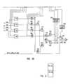
- Fig. 3shows the internal circuit of the programmable neural logic cell. It consists of four inputs, (A, B, C and F1) 102, 104, 106 and 108 which are passed to gates 122, 124, 126 and 128 whose other input comes from the master-slave latches 212, 214, 216 and 218. These latches are collectively called the invert control. Depending on the values contained in latches 212, 214, 216 or 218, the outputs of gates 122, 124, 126 or 128 are either the input values A, B, C, F1 or their inverses.
- the internal structure of gates 122, 124, 126 and 128is shown in Fig. 4.
- Each oneconsists of two inverters 132, 134, two AND gates 136, 138 and an OR gate 139.
- the inputis supplied along line 130 whilst the value held in the master-slave latch 212, 214, 216, 218 is supplied along 131.
- the output of the gateis produced by OR gate 139. It can be seen, by considering the logic of the circuit, that if the value 0 is supplied from the latch 212, 214, 216 or 218 then the output of the gate will be the same as its input 130. However, if line 131 has value 1 on it, then the output will be the inverse of the input 130.
- the output of the gates 122, 124, 126 and 128is each passed to a separate AND gate 162, 164, 166 or 168 whose other input comes from the 'enable control' formed by master-slave latches 222, 224, 226, 228. These gates select which of the inputs 102, 104, 106, 108 or inverted inputs are to be enabled and hence operated on in the cell.
- the outputs of these AND gates 162, 164, 166 and 168are passed to both an XOR gate 172, 174 or 179 and an OR gate 182, 184 or 189.
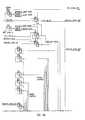
- Initialising the cell before operationbegins involves loading the invert control 212, 214, 216, 218 and enable control 222, 224, 226, 228 latches with values to indicate which inputs are to be enabled and which inverted. Since the latches are connected together as a chain, this is a simple matter of providing the required values at Ena/Inv_Scan_In 200 and clocking them through each latch. To save wiring on the chip, it is possible that the invert and enable control latches of several cells are connected together in a chain (as is shown on Fig. 3) so that the values to be placed in other cells are clocked into one cell using Ena/Inv_Scan_In 200 and out using Ena/Inv_Scan_Out 202.
- the Boolean select latches 252 and 254 and the clock select SRL 250are loaded through the Boolean Scan In 240, Boolean Scan Out 258 and other connected lines in a similar manner.
- the signals transferred into the cell on the Neu_Scan_In 246 lineare clocked from latch 248 to latch 249 and then out to the next cell on Neu_Scan_Out 247.
- the latch 248is connected to Clock mode select 262 which is in turn connected to the Boolean select latches 252 and 254 where its value determines whether these latches 252, 254 are responsive to the inputs on the Boolean Sell 242 and Boolean Sel2 244 lines.
- Clock Mode Select 260is connected to latch 249 and controls the SRL 250. It determines whether the value initially loaded into the SRL 250 is maintained during cell operation (Shift mode) or whether it can be changed during operation by the Clk_Sel input line 251 (Neuro mode).
- Clk - Sel 251is connected to the output of a previous cell as is shown on Fig. 7.
- the output of SRL 250is connected to clock mode 264 which causes the data SRL 232 to operate in either 'system clock mode' or in 'flush mode'. In the latter mode, both the master and slave latches are continuously active during operation and data is transferred immediately between cells rather than being held in SRL 232 until the next clock cycle. During testing of the circuit, however, the cell will be operated in system clock mode.
- the normal (i.e. non-neural) operation of the cellis straightforward.
- the required logicis loaded from Ena/Inv_Scan_In 200 and the data input at 102, 104, 106 and 108.
- the resultappears at SRL 232 from where it can be transferred out using Data_Scan_In 230.
- the whole cellcan operate in either system clock mode or flush mode depending on clock cycle time requirements.
- the neural mode of the cellis controlled by Clock Mode Select 262. It controls whether the Boolean select latches 252 and 254 operate with the logic mode clocked in through Boolean Scan In 240 or whether they are responsive to signals on lines Boolean Sell 242 and Boolean_Sel2 244.
- the output of gates 179, 189, 192 or 194 selected by the Boolean decoder 256will be altered by changes in these signals and hence the cell output, Q, 234 will be changed.
- the inputs 102, 104, 106 and 108do not necessarily have to change during this cycle.
- the values of Clk_Set 251, Boolean Sell 242 and Boolean Sel2 244may be derived either from inputs generated off the chip or be the results of operations from previous logic cells as shown on Fig. 7.
- the second mode of neural operationinvolves altering the invert control 212, 214, 216 and 218 and expand control 222, 224, 226 and 228 latches. After these have been initially set, their values can be changed during operation by having an extra input to the latch which will determine whether a data input to the cell 102, 104, 106 or 108 should be inverted or ignored during a cycle of operation. These extra latch inputs may either be generated off chip or be themselves the result of a logic operation by another cell as shown on Fig. 6.
- Fig. 5shows another embodiment of this invention. Instead of having four inputs to each cell, this figure shows eight inputs to the cell and hence each cell has been termed an 'Octopus'.
- the operation of this cellis exactly the same as that described above except that it is now possible to use up to eight different data inputs which allows a greater variety of applications. In principle, it would be possible to have as many data inputs to one single cell as are required, however, this will lead to complex internal cell configurations which may cause manufacturing problems. If more than eight inputs are required, then it will be better to connect two or more cells together rather than trying to produce one huge cell.
- a balanced designmay consist of a mix of small cells (4 inputs) and large cells (8 inputs).
- Fig. 6shows a typical data net in which octopus cells can be found. It is seen that the outputs of a number of cells are connected to the data inputs of the cells. These connections are formed by hardwiring. Connections between the output of some octopus cells and the Clk Sel, Boolean_Sel1 and Boolean_Sel2 inputs of Figs. 3 and 5 (the so-called 'neural connections') are shown on Fig. 7. It should be noted that the wiring is only shown seperately on two different figures for simplicity. In practice similar logic cells on the same chip will be connected using the two different but overlapping wiring networks.
Landscapes
- Engineering & Computer Science (AREA)
- Physics & Mathematics (AREA)
- Theoretical Computer Science (AREA)
- Computing Systems (AREA)
- General Engineering & Computer Science (AREA)
- Mathematical Physics (AREA)
- Health & Medical Sciences (AREA)
- Life Sciences & Earth Sciences (AREA)
- Biomedical Technology (AREA)
- Biophysics (AREA)
- Neurology (AREA)
- Artificial Intelligence (AREA)
- Computational Linguistics (AREA)
- Data Mining & Analysis (AREA)
- Evolutionary Computation (AREA)
- General Health & Medical Sciences (AREA)
- Molecular Biology (AREA)
- General Physics & Mathematics (AREA)
- Software Systems (AREA)
- Computer Hardware Design (AREA)
- Logic Circuits (AREA)
- Design And Manufacture Of Integrated Circuits (AREA)
Abstract

Description
- The invention relates to a programmable logic device whose logic can be set at the beginning of its operation and which can be changed during operation. A number of these devices are connected together such that the output of one device can alter the internal logic of another.
- Programmable logic or gate arrays have been known for some time. These arrays allow the designer to use a small number of standard components rather than relying on customised designs when designing a logic circuit. Such arrays are produced, for example, by XILINX. In this company's CMOS-based XC3000 Logic Cell (TM) Array Family, the functions of the array are established by a configuration program which is loaded into an internal, distributed array of configuration memory cells. This configuration program is loaded into the array at power-up and may be reloaded on command. The program data resides external to the logic cell in an EEPROM, EPROM or ROM on the application circuit board or on a floppy disc or hard disc. The logic within the cells can be changed whenever required, however, this involves stopping the current operation of the circuit whilst the alterations are carried out.
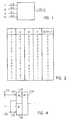
- Attention recently has been focused on neural or neuronal logic devices. These operate by weighting the values of the inputs into the logic device and producing an output which is a function of all the inputs. An example of this is shown by the device in Fig. 1 whose output is either 1 or 0 but whose inputs take various values. For example input 1 (i1) has a weighting value of 0.8, input 2 (i2) of 0.6, input 3 (i3) is 0.1 and input 4 (i4) is 0.4. It might then be decided that if i1 + 12 + 13 + i4> 1 then output = 1, otherwise output = 0
- A truth table for this device would have the form shown in Fig. 2. It is possible for the weightings of the individual inputs to be changed using a feedback mechanism; the devices can then undergo a 'learning' process in which the weightings of each input are altered to give the required output in response to a series of inputs. Such a process mimics the learning process of the human brain - hence the name. The action of learning is described in more detail in the German magazine, CHIP,
Nr 4, April 1990, pp 11-16, "Auf dem Weg zur Denkmaschine" by THOMAS. - A reconfigurable neural network was presented at the 1990 International Solid State Circuits Conference (see Digest of Technical Papers, 33, pp 144-145, "A reconfigurable CMOS neural network" by GRAF et al). In this device the output currents of the individual 'neurons' are summed on a wire and the result compared with a reference value to give the output. The amount of current from each neuron is altered ('weighted') by programming the width of each FET transistor within the neutron using switches. In this example, the final output of the network could be altered by either varying the reference current value or by changing the amount of current each 'neuron' outputs. The logic of the device is, however, set by the hardwiring within the network.
- The invention described is a novel combination of all of these prior art elements. It consists of a series of logic cells, the internal logic of which can be set to any desired logical value at power up. During operation, the number of inputs to the cell can be altered and its internal logic varied. The commands for changing the cell's function can be either supplied from an off-chip processor or as the results of the logic operation of another cell. The cells are connected together to form a network whose output can be adjusted to take certain values upon the receipt of specified inputs.
- Fig. 1 shows a neural logic cell with weighted inputs.
- Fig. 2 is the truth table for the cell shown in Fig. 1.
- Fig. 3 shows a neural logic cell according to this invention with four inputs.
- Fig. 4 shows the internal structure of the gates to which each input of the logic cell is connected.
- Fig. 5 shows a further embodiment of the neural programmable logic cell with eight inputs.
- Fig. 6 shows a network of neural logic cells whose outputs are connected to logical inputs.
- Fig. 7 shows a network of neural logic cells whose outputs are connected to neural inputs.
- Fig. 3 shows the internal circuit of the programmable neural logic cell. It consists of four inputs, (A, B, C and F1) 102, 104, 106 and 108 which are passed to
gates slave latches latches gates gates inverters gates OR gate 139. The input is supplied alongline 130 whilst the value held in the master-slave latch gate 139. It can be seen, by considering the logic of the circuit, that if thevalue 0 is supplied from thelatch input 130. However, ifline 131 hasvalue 1 on it, then the output will be the inverse of theinput 130. - The output of the
gates separate AND gate slave latches inputs gates XOR gate OR gate final XOR gate 179 and final ORgate 189 are then connected both directly and throughinverters Boolean decoder 256. Master-slave latches 252 and 254 are connected (via slave output latch) to theBoolean decoder 256. Their value determines which of the four outputs is passed to the Data Shift Register Latch (SRL) 232 and hence forms the output of the cell Q at 234. - Careful consideration of the circuit will show that it is possible to carry out all possible logic functions for the four inputs. It is clear from the logic of the circuit how XOR or OR combinations of the input can be obtained; the AND function is obtained by using the results of DeMorgan's theorem which states that result, Q, of an AND operation can be expressed in two ways: Q = A AND B = NOT ( (NOT A) OR (NOT B))
- This result can be generalised for the case of four (or more) inputs. Since the described logic circuit contains inverters for inverting the input (122, 124, 126, 128) and the output (192, 194), it can be seen that the circuit can also perform this fuction.
- Initialising the cell before operation begins involves loading the
invert control control latches 252 and 254 and the clock selectSRL 250 are loaded through the Boolean Scan In 240, Boolean Scan Out 258 and other connected lines in a similar manner. - The signals transferred into the cell on the Neu_Scan_In 246 line are clocked from
latch 248 tolatch 249 and then out to the next cell on Neu_Scan_Out 247. Thelatch 248 is connected to Clock mode select 262 which is in turn connected to the Booleanselect latches 252 and 254 where its value determines whether theselatches 252, 254 are responsive to the inputs on theBoolean Sell 242 andBoolean Sel2 244 lines.Clock Mode Select 260 is connected to latch 249 and controls theSRL 250. It determines whether the value initially loaded into theSRL 250 is maintained during cell operation (Shift mode) or whether it can be changed during operation by the Clk_Sel input line 251 (Neuro mode). Clk-Sel 251 is connected to the output of a previous cell as is shown on Fig. 7. The output ofSRL 250 is connected toclock mode 264 which causes thedata SRL 232 to operate in either 'system clock mode' or in 'flush mode'. In the latter mode, both the master and slave latches are continuously active during operation and data is transferred immediately between cells rather than being held inSRL 232 until the next clock cycle. During testing of the circuit, however, the cell will be operated in system clock mode. - The normal (i.e. non-neural) operation of the cell is straightforward. The required logic is loaded from Ena/
Inv_Scan_In 200 and the data input at 102, 104, 106 and 108. The result appears atSRL 232 from where it can be transferred out usingData_Scan_In 230. The whole cell can operate in either system clock mode or flush mode depending on clock cycle time requirements. - There are two forms of neural operation. In the first form, the neural mode of the cell is controlled by
Clock Mode Select 262. It controls whether the Booleanselect latches 252 and 254 operate with the logic mode clocked in through Boolean Scan In 240 or whether they are responsive to signals on linesBoolean Sell 242 andBoolean_Sel2 244. The output ofgates Boolean decoder 256 will be altered by changes in these signals and hence the cell output, Q, 234 will be changed. It should be noted that theinputs Clk_Set 251,Boolean Sell 242 andBoolean Sel2 244 may be derived either from inputs generated off the chip or be the results of operations from previous logic cells as shown on Fig. 7. - The second mode of neural operation involves altering the
invert control control cell - Fig. 5 shows another embodiment of this invention. Instead of having four inputs to each cell, this figure shows eight inputs to the cell and hence each cell has been termed an 'Octopus'. The operation of this cell is exactly the same as that described above except that it is now possible to use up to eight different data inputs which allows a greater variety of applications. In principle, it would be possible to have as many data inputs to one single cell as are required, however, this will lead to complex internal cell configurations which may cause manufacturing problems. If more than eight inputs are required, then it will be better to connect two or more cells together rather than trying to produce one huge cell. A balanced design may consist of a mix of small cells (4 inputs) and large cells (8 inputs).
- Fig. 6 shows a typical data net in which octopus cells can be found. It is seen that the outputs of a number of cells are connected to the data inputs of the cells. These connections are formed by hardwiring. Connections between the output of some octopus cells and the Clk Sel, Boolean_Sel1 and Boolean_Sel2 inputs of Figs. 3 and 5 (the so-called 'neural connections') are shown on Fig. 7. It should be noted that the wiring is only shown seperately on two different figures for simplicity. In practice similar logic cells on the same chip will be connected using the two different but overlapping wiring networks.
Claims (13)
Priority Applications (4)
| Application Number | Priority Date | Filing Date | Title |
|---|---|---|---|
| EP90117818AEP0476159B1 (en) | 1990-09-15 | 1990-09-15 | Programmable neural logic device |
| DE69029390TDE69029390T2 (en) | 1990-09-15 | 1990-09-15 | Programmable circuit for neural logic |
| JP3193423AJP2548852B2 (en) | 1990-09-15 | 1991-07-08 | Programmable logic cell |
| US07/758,642US5218245A (en) | 1990-09-15 | 1991-09-12 | Programmable neural logic device |
Applications Claiming Priority (1)
| Application Number | Priority Date | Filing Date | Title |
|---|---|---|---|
| EP90117818AEP0476159B1 (en) | 1990-09-15 | 1990-09-15 | Programmable neural logic device |
Publications (2)
| Publication Number | Publication Date |
|---|---|
| EP0476159A1true EP0476159A1 (en) | 1992-03-25 |
| EP0476159B1 EP0476159B1 (en) | 1996-12-11 |
Family
ID=8204473
Family Applications (1)
| Application Number | Title | Priority Date | Filing Date |
|---|---|---|---|
| EP90117818AExpired - LifetimeEP0476159B1 (en) | 1990-09-15 | 1990-09-15 | Programmable neural logic device |
Country Status (4)
| Country | Link |
|---|---|
| US (1) | US5218245A (en) |
| EP (1) | EP0476159B1 (en) |
| JP (1) | JP2548852B2 (en) |
| DE (1) | DE69029390T2 (en) |
Cited By (22)
| Publication number | Priority date | Publication date | Assignee | Title |
|---|---|---|---|---|
| EP0841621A1 (en)* | 1996-11-06 | 1998-05-13 | Sowa Institute of Technology Co., Ltd. | Learning methods in binary systems |
| EP0978791A4 (en)* | 1998-02-20 | 2000-07-05 | Sowa Inst Of Technology Co Ltd | METHOD FOR LEARNING A BINARY SYSTEM |
| WO2013090092A1 (en)* | 2011-12-15 | 2013-06-20 | Micron Technology, Inc. | Boolean logic in a state machine lattice |
| US9448965B2 (en) | 2013-03-15 | 2016-09-20 | Micron Technology, Inc. | Receiving data streams in parallel and providing a first portion of data to a first state machine engine and a second portion to a second state machine |
| US9524248B2 (en) | 2012-07-18 | 2016-12-20 | Micron Technology, Inc. | Memory management for a hierarchical memory system |
| US9703574B2 (en) | 2013-03-15 | 2017-07-11 | Micron Technology, Inc. | Overflow detection and correction in state machine engines |
| US10019311B2 (en) | 2016-09-29 | 2018-07-10 | Micron Technology, Inc. | Validation of a symbol response memory |
| US10146555B2 (en) | 2016-07-21 | 2018-12-04 | Micron Technology, Inc. | Adaptive routing to avoid non-repairable memory and logic defects on automata processor |
| US10268602B2 (en) | 2016-09-29 | 2019-04-23 | Micron Technology, Inc. | System and method for individual addressing |
| US10417236B2 (en) | 2008-12-01 | 2019-09-17 | Micron Technology, Inc. | Devices, systems, and methods to synchronize simultaneous DMA parallel processing of a single data stream by multiple devices |
| US10430210B2 (en) | 2014-12-30 | 2019-10-01 | Micron Technology, Inc. | Systems and devices for accessing a state machine |
| US10592450B2 (en) | 2016-10-20 | 2020-03-17 | Micron Technology, Inc. | Custom compute cores in integrated circuit devices |
| US10684983B2 (en) | 2009-12-15 | 2020-06-16 | Micron Technology, Inc. | Multi-level hierarchical routing matrices for pattern-recognition processors |
| US10691964B2 (en) | 2015-10-06 | 2020-06-23 | Micron Technology, Inc. | Methods and systems for event reporting |
| US10769099B2 (en) | 2014-12-30 | 2020-09-08 | Micron Technology, Inc. | Devices for time division multiplexing of state machine engine signals |
| US10846103B2 (en) | 2015-10-06 | 2020-11-24 | Micron Technology, Inc. | Methods and systems for representing processing resources |
| US10929764B2 (en) | 2016-10-20 | 2021-02-23 | Micron Technology, Inc. | Boolean satisfiability |
| US10977309B2 (en) | 2015-10-06 | 2021-04-13 | Micron Technology, Inc. | Methods and systems for creating networks |
| US11023758B2 (en) | 2009-01-07 | 2021-06-01 | Micron Technology, Inc. | Buses for pattern-recognition processors |
| US11366675B2 (en) | 2014-12-30 | 2022-06-21 | Micron Technology, Inc. | Systems and devices for accessing a state machine |
| US11488645B2 (en) | 2012-04-12 | 2022-11-01 | Micron Technology, Inc. | Methods for reading data from a storage buffer including delaying activation of a column select |
| US12197510B2 (en) | 2016-10-20 | 2025-01-14 | Micron Technology, Inc. | Traversal of S portion of a graph problem to be solved using automata processor |
Families Citing this family (6)
| Publication number | Priority date | Publication date | Assignee | Title |
|---|---|---|---|---|
| FR2704669B1 (en)* | 1993-04-29 | 1995-06-30 | France Telecom | NEURONAL NETWORK SYSTEM FOR SIGNAL PROCESSING, ESPECIALLY FOR ANALYSIS AND SYNTHESIS OF IMAGES. |
| US6140838A (en) | 1995-04-21 | 2000-10-31 | Johnson; Mark B. | High density and high speed magneto-electronic logic family |
| US6741494B2 (en)* | 1995-04-21 | 2004-05-25 | Mark B. Johnson | Magnetoelectronic memory element with inductively coupled write wires |
| US5732246A (en)* | 1995-06-07 | 1998-03-24 | International Business Machines Corporation | Programmable array interconnect latch |
| US5651013A (en)* | 1995-11-14 | 1997-07-22 | International Business Machines Corporation | Programmable circuits for test and operation of programmable gate arrays |
| US6687864B1 (en)* | 2000-06-08 | 2004-02-03 | Cypress Semiconductor Corp. | Macro-cell flip-flop with scan-in input |
Citations (3)
| Publication number | Priority date | Publication date | Assignee | Title |
|---|---|---|---|---|
| DE3606406A1 (en)* | 1985-02-27 | 1986-08-28 | Xilinx, Inc., San Jose, Calif. | CONFIGURABLE LOGIC ELEMENT |
| EP0322966A1 (en)* | 1987-12-23 | 1989-07-05 | Laboratoires D'electronique Philips | Neural network circuit and structure |
| EP0340890A2 (en)* | 1988-05-05 | 1989-11-08 | Altera Corporation | Programmable logic device with array blocks connected via a programmable interconnect array |
Family Cites Families (5)
| Publication number | Priority date | Publication date | Assignee | Title |
|---|---|---|---|---|
| US4612459A (en)* | 1984-05-31 | 1986-09-16 | Rca Corporation | Programmable buffer selectively settable to operate in different modes |
| US5019736A (en)* | 1986-11-07 | 1991-05-28 | Concurrent Logic, Inc. | Programmable logic cell and array |
| US5055897A (en)* | 1988-07-27 | 1991-10-08 | Intel Corporation | Semiconductor cell for neural network and the like |
| US4999687A (en)* | 1990-04-25 | 1991-03-12 | At&T Bell Laboratories | Logic element and article comprising the element |
| US5093900A (en)* | 1991-02-13 | 1992-03-03 | At&T Bell Laboratories | Reconfigurable neural network |
- 1990
- 1990-09-15EPEP90117818Apatent/EP0476159B1/ennot_activeExpired - Lifetime
- 1990-09-15DEDE69029390Tpatent/DE69029390T2/ennot_activeExpired - Fee Related
- 1991
- 1991-07-08JPJP3193423Apatent/JP2548852B2/ennot_activeExpired - Lifetime
- 1991-09-12USUS07/758,642patent/US5218245A/ennot_activeExpired - Lifetime
Patent Citations (3)
| Publication number | Priority date | Publication date | Assignee | Title |
|---|---|---|---|---|
| DE3606406A1 (en)* | 1985-02-27 | 1986-08-28 | Xilinx, Inc., San Jose, Calif. | CONFIGURABLE LOGIC ELEMENT |
| EP0322966A1 (en)* | 1987-12-23 | 1989-07-05 | Laboratoires D'electronique Philips | Neural network circuit and structure |
| EP0340890A2 (en)* | 1988-05-05 | 1989-11-08 | Altera Corporation | Programmable logic device with array blocks connected via a programmable interconnect array |
Non-Patent Citations (1)
| Title |
|---|
| IEEE INTERNATIONAL SOLID STATE CIRCUITS CONFERENCE. 15 February 1990, NEW YORK US pages 144 - 145; H. P. Graf: "A Reconfigurable CMOS Neural Network"* |
Cited By (54)
| Publication number | Priority date | Publication date | Assignee | Title |
|---|---|---|---|---|
| EP0841621A1 (en)* | 1996-11-06 | 1998-05-13 | Sowa Institute of Technology Co., Ltd. | Learning methods in binary systems |
| EP0978791A4 (en)* | 1998-02-20 | 2000-07-05 | Sowa Inst Of Technology Co Ltd | METHOD FOR LEARNING A BINARY SYSTEM |
| US10838966B2 (en) | 2008-12-01 | 2020-11-17 | Micron Technology, Inc. | Devices, systems, and methods to synchronize simultaneous DMA parallel processing of a single data stream by multiple devices |
| US10417236B2 (en) | 2008-12-01 | 2019-09-17 | Micron Technology, Inc. | Devices, systems, and methods to synchronize simultaneous DMA parallel processing of a single data stream by multiple devices |
| US12067767B2 (en) | 2009-01-07 | 2024-08-20 | Micron Technology, Inc. | Buses for pattern-recognition processors |
| US11023758B2 (en) | 2009-01-07 | 2021-06-01 | Micron Technology, Inc. | Buses for pattern-recognition processors |
| US11226926B2 (en) | 2009-12-15 | 2022-01-18 | Micron Technology, Inc. | Multi-level hierarchical routing matrices for pattern-recognition processors |
| US10684983B2 (en) | 2009-12-15 | 2020-06-16 | Micron Technology, Inc. | Multi-level hierarchical routing matrices for pattern-recognition processors |
| US11768798B2 (en) | 2009-12-15 | 2023-09-26 | Micron Technology, Inc. | Multi-level hierarchical routing matrices for pattern-recognition processors |
| US9118327B2 (en) | 2011-12-15 | 2015-08-25 | Micron Technology, Inc. | Boolean logic in a state machine lattice |
| WO2013090092A1 (en)* | 2011-12-15 | 2013-06-20 | Micron Technology, Inc. | Boolean logic in a state machine lattice |
| US9866218B2 (en) | 2011-12-15 | 2018-01-09 | Micron Technology, Inc. | Boolean logic in a state machine lattice |
| US9509312B2 (en) | 2011-12-15 | 2016-11-29 | Micron Technology, Inc. | Boolean logic in a state machine lattice |
| US8593175B2 (en) | 2011-12-15 | 2013-11-26 | Micron Technology, Inc. | Boolean logic in a state machine lattice |
| US12347519B2 (en) | 2012-04-12 | 2025-07-01 | Micron Technology, Inc. | Methods for reading data from a storage buffer including delaying activation of a column select |
| US11488645B2 (en) | 2012-04-12 | 2022-11-01 | Micron Technology, Inc. | Methods for reading data from a storage buffer including delaying activation of a column select |
| US9524248B2 (en) | 2012-07-18 | 2016-12-20 | Micron Technology, Inc. | Memory management for a hierarchical memory system |
| US10089242B2 (en) | 2012-07-18 | 2018-10-02 | Micron Technology, Inc. | Memory management for a hierarchical memory system |
| US10831672B2 (en) | 2012-07-18 | 2020-11-10 | Micron Technology, Inc | Memory management for a hierarchical memory system |
| US10067901B2 (en) | 2013-03-15 | 2018-09-04 | Micron Technology, Inc. | Methods and apparatuses for providing data received by a state machine engine |
| US9448965B2 (en) | 2013-03-15 | 2016-09-20 | Micron Technology, Inc. | Receiving data streams in parallel and providing a first portion of data to a first state machine engine and a second portion to a second state machine |
| US10372653B2 (en) | 2013-03-15 | 2019-08-06 | Micron Technology, Inc. | Apparatuses for providing data received by a state machine engine |
| US11775320B2 (en) | 2013-03-15 | 2023-10-03 | Micron Technology, Inc. | Overflow detection and correction in state machine engines |
| US10606787B2 (en) | 2013-03-15 | 2020-03-31 | Mircron Technology, Inc. | Methods and apparatuses for providing data received by a state machine engine |
| US9747242B2 (en) | 2013-03-15 | 2017-08-29 | Micron Technology, Inc. | Methods and apparatuses for providing data received by a plurality of state machine engines |
| US11016790B2 (en) | 2013-03-15 | 2021-05-25 | Micron Technology, Inc. | Overflow detection and correction in state machine engines |
| US10929154B2 (en) | 2013-03-15 | 2021-02-23 | Micron Technology, Inc. | Overflow detection and correction in state machine engines |
| US9703574B2 (en) | 2013-03-15 | 2017-07-11 | Micron Technology, Inc. | Overflow detection and correction in state machine engines |
| US11366675B2 (en) | 2014-12-30 | 2022-06-21 | Micron Technology, Inc. | Systems and devices for accessing a state machine |
| US10430210B2 (en) | 2014-12-30 | 2019-10-01 | Micron Technology, Inc. | Systems and devices for accessing a state machine |
| US10769099B2 (en) | 2014-12-30 | 2020-09-08 | Micron Technology, Inc. | Devices for time division multiplexing of state machine engine signals |
| US12130774B2 (en) | 2014-12-30 | 2024-10-29 | Micron Technology, Inc. | Devices for time division multiplexing of state machine engine signals |
| US11947979B2 (en) | 2014-12-30 | 2024-04-02 | Micron Technology, Inc. | Systems and devices for accessing a state machine |
| US11580055B2 (en) | 2014-12-30 | 2023-02-14 | Micron Technology, Inc. | Devices for time division multiplexing of state machine engine signals |
| US10977309B2 (en) | 2015-10-06 | 2021-04-13 | Micron Technology, Inc. | Methods and systems for creating networks |
| US10691964B2 (en) | 2015-10-06 | 2020-06-23 | Micron Technology, Inc. | Methods and systems for event reporting |
| US12174888B2 (en) | 2015-10-06 | 2024-12-24 | Micron Technology, Inc. | Methods and systems for creating automata networks |
| US10846103B2 (en) | 2015-10-06 | 2020-11-24 | Micron Technology, Inc. | Methods and systems for representing processing resources |
| US11977902B2 (en) | 2015-10-06 | 2024-05-07 | Micron Technology, Inc. | Methods and systems for event reporting |
| US11816493B2 (en) | 2015-10-06 | 2023-11-14 | Micron Technology, Inc. | Methods and systems for representing processing resources |
| US10698697B2 (en) | 2016-07-21 | 2020-06-30 | Micron Technology, Inc. | Adaptive routing to avoid non-repairable memory and logic defects on automata processor |
| US10146555B2 (en) | 2016-07-21 | 2018-12-04 | Micron Technology, Inc. | Adaptive routing to avoid non-repairable memory and logic defects on automata processor |
| US10339071B2 (en) | 2016-09-29 | 2019-07-02 | Micron Technology, Inc. | System and method for individual addressing |
| US10789182B2 (en) | 2016-09-29 | 2020-09-29 | Micron Technology, Inc. | System and method for individual addressing |
| US10268602B2 (en) | 2016-09-29 | 2019-04-23 | Micron Technology, Inc. | System and method for individual addressing |
| US10402265B2 (en) | 2016-09-29 | 2019-09-03 | Micron Technology, Inc. | Validation of a symbol response memory |
| US10949290B2 (en) | 2016-09-29 | 2021-03-16 | Micron Technology, Inc. | Validation of a symbol response memory |
| US10521366B2 (en) | 2016-09-29 | 2019-12-31 | Micron Technology, Inc. | System and method for individual addressing |
| US10019311B2 (en) | 2016-09-29 | 2018-07-10 | Micron Technology, Inc. | Validation of a symbol response memory |
| US11829311B2 (en) | 2016-10-20 | 2023-11-28 | Micron Technology, Inc. | Custom compute cores in integrated circuit devices |
| US10929764B2 (en) | 2016-10-20 | 2021-02-23 | Micron Technology, Inc. | Boolean satisfiability |
| US11194747B2 (en) | 2016-10-20 | 2021-12-07 | Micron Technology, Inc. | Custom compute cores in integrated circuit devices |
| US10592450B2 (en) | 2016-10-20 | 2020-03-17 | Micron Technology, Inc. | Custom compute cores in integrated circuit devices |
| US12197510B2 (en) | 2016-10-20 | 2025-01-14 | Micron Technology, Inc. | Traversal of S portion of a graph problem to be solved using automata processor |
Also Published As
| Publication number | Publication date |
|---|---|
| JP2548852B2 (en) | 1996-10-30 |
| DE69029390T2 (en) | 1997-06-12 |
| EP0476159B1 (en) | 1996-12-11 |
| DE69029390D1 (en) | 1997-01-23 |
| US5218245A (en) | 1993-06-08 |
| JPH04227116A (en) | 1992-08-17 |
Similar Documents
| Publication | Publication Date | Title |
|---|---|---|
| US5218245A (en) | Programmable neural logic device | |
| KR940010679B1 (en) | Integrated circuit with programmable logic circuit | |
| KR100235812B1 (en) | Shift register and programmable logic circuit and programmable logic circuit system | |
| US4225957A (en) | Testing macros embedded in LSI chips | |
| US6150837A (en) | Enhanced field programmable gate array | |
| US4771285A (en) | Programmable logic cell with flexible clocking and flexible feedback | |
| KR0130760B1 (en) | Semiconductor integrated circuit | |
| CA2038162C (en) | Programmable connector | |
| KR100187299B1 (en) | Input Row Driver for Programmable Logic Units | |
| US5121394A (en) | Method of organizing programmable logic array devices for board testability | |
| US5764076A (en) | Circuit for partially reprogramming an operational programmable logic device | |
| JPH09231788A5 (en) | ||
| EP0866558A2 (en) | Programmable logic array device with random access memory configurable as product terms | |
| US4983959A (en) | Logic output macrocell | |
| JPH07507194A (en) | Electrically programmable logic device chip with hybrid configuration optimized for both speed and flexibility | |
| KR920004936A (en) | Programmable Logic Devices Input / Output Macrocells | |
| US4761570A (en) | Programmable logic device with programmable signal inhibition and inversion means | |
| US5497107A (en) | Multiple, selectable PLAS having shared inputs and outputs | |
| US6879185B2 (en) | Low power clock distribution scheme | |
| US5075576A (en) | Field-programmable logic device with programmable foldback to control number of logic levels | |
| US5298803A (en) | Programmable logic device having low power microcells with selectable registered and combinatorial output signals | |
| JPH0568729B2 (en) | ||
| EP1126614B1 (en) | Programmable logic arrays | |
| US4851716A (en) | Single plane dynamic decoder | |
| US5977792A (en) | Configurable logic circuit and method |
Legal Events
| Date | Code | Title | Description |
|---|---|---|---|
| PUAI | Public reference made under article 153(3) epc to a published international application that has entered the european phase | Free format text:ORIGINAL CODE: 0009012 | |
| AK | Designated contracting states | Kind code of ref document:A1 Designated state(s):DE FR GB | |
| 17P | Request for examination filed | Effective date:19920817 | |
| 17Q | First examination report despatched | Effective date:19940411 | |
| GRAG | Despatch of communication of intention to grant | Free format text:ORIGINAL CODE: EPIDOS AGRA | |
| GRAH | Despatch of communication of intention to grant a patent | Free format text:ORIGINAL CODE: EPIDOS IGRA | |
| GRAH | Despatch of communication of intention to grant a patent | Free format text:ORIGINAL CODE: EPIDOS IGRA | |
| GRAA | (expected) grant | Free format text:ORIGINAL CODE: 0009210 | |
| AK | Designated contracting states | Kind code of ref document:B1 Designated state(s):DE FR GB | |
| PG25 | Lapsed in a contracting state [announced via postgrant information from national office to epo] | Ref country code:FR Effective date:19961211 | |
| REF | Corresponds to: | Ref document number:69029390 Country of ref document:DE Date of ref document:19970123 | |
| EN | Fr: translation not filed | ||
| PG25 | Lapsed in a contracting state [announced via postgrant information from national office to epo] | Ref country code:GB Free format text:LAPSE BECAUSE OF NON-PAYMENT OF DUE FEES Effective date:19970915 | |
| PGFP | Annual fee paid to national office [announced via postgrant information from national office to epo] | Ref country code:DE Payment date:19970926 Year of fee payment:8 | |
| PLBE | No opposition filed within time limit | Free format text:ORIGINAL CODE: 0009261 | |
| STAA | Information on the status of an ep patent application or granted ep patent | Free format text:STATUS: NO OPPOSITION FILED WITHIN TIME LIMIT | |
| 26N | No opposition filed | ||
| GBPC | Gb: european patent ceased through non-payment of renewal fee | Effective date:19970915 | |
| PG25 | Lapsed in a contracting state [announced via postgrant information from national office to epo] | Ref country code:DE Free format text:LAPSE BECAUSE OF NON-PAYMENT OF DUE FEES Effective date:19990701 |