EP0461990B1 - Micropoint cathode electron source - Google Patents
Micropoint cathode electron sourceDownload PDFInfo
- Publication number
- EP0461990B1 EP0461990B1EP91401536AEP91401536AEP0461990B1EP 0461990 B1EP0461990 B1EP 0461990B1EP 91401536 AEP91401536 AEP 91401536AEP 91401536 AEP91401536 AEP 91401536AEP 0461990 B1EP0461990 B1EP 0461990B1
- Authority
- EP
- European Patent Office
- Prior art keywords
- electron source
- source according
- resistive coating
- cathode
- resistive layer
- Prior art date
- Legal status (The legal status is an assumption and is not a legal conclusion. Google has not performed a legal analysis and makes no representation as to the accuracy of the status listed.)
- Expired - Lifetime
Links
- 239000004020conductorSubstances0.000claimsdescription50
- 229910052710siliconInorganic materials0.000claimsdescription10
- 239000010703siliconSubstances0.000claimsdescription10
- 239000000463materialSubstances0.000claimsdescription6
- 239000011248coating agentSubstances0.000claims8
- 238000000576coating methodMethods0.000claims8
- VAYOSLLFUXYJDT-RDTXWAMCSA-NLysergic acid diethylamideChemical compoundC1=CC(C=2[C@H](N(C)C[C@@H](C=2)C(=O)N(CC)CC)C2)=C3C2=CNC3=C1VAYOSLLFUXYJDT-RDTXWAMCSA-N0.000claims7
- VYPSYNLAJGMNEJ-UHFFFAOYSA-NSilicium dioxideChemical compoundO=[Si]=OVYPSYNLAJGMNEJ-UHFFFAOYSA-N0.000description10
- XUIMIQQOPSSXEZ-UHFFFAOYSA-NSiliconChemical compound[Si]XUIMIQQOPSSXEZ-UHFFFAOYSA-N0.000description9
- 230000000694effectsEffects0.000description7
- 238000000265homogenisationMethods0.000description7
- 230000015556catabolic processEffects0.000description6
- 239000000377silicon dioxideSubstances0.000description5
- UQSXHKLRYXJYBZ-UHFFFAOYSA-NIron oxideChemical compound[Fe]=OUQSXHKLRYXJYBZ-UHFFFAOYSA-N0.000description4
- 229910003437indium oxideInorganic materials0.000description3
- PJXISJQVUVHSOJ-UHFFFAOYSA-Nindium(iii) oxideChemical compound[O-2].[O-2].[O-2].[In+3].[In+3]PJXISJQVUVHSOJ-UHFFFAOYSA-N0.000description3
- 238000004519manufacturing processMethods0.000description3
- 239000011159matrix materialSubstances0.000description3
- 229910052750molybdenumInorganic materials0.000description3
- 229910052804chromiumInorganic materials0.000description2
- 229910052681coesiteInorganic materials0.000description2
- 229910052906cristobaliteInorganic materials0.000description2
- 230000001419dependent effectEffects0.000description2
- 230000005284excitationEffects0.000description2
- 239000011521glassSubstances0.000description2
- 229910052751metalInorganic materials0.000description2
- 239000002184metalSubstances0.000description2
- 229910052758niobiumInorganic materials0.000description2
- 238000001020plasma etchingMethods0.000description2
- 235000012239silicon dioxideNutrition0.000description2
- 238000004544sputter depositionMethods0.000description2
- 229910052682stishoviteInorganic materials0.000description2
- 239000000758substrateSubstances0.000description2
- XOLBLPGZBRYERU-UHFFFAOYSA-Ntin dioxideChemical compoundO=[Sn]=OXOLBLPGZBRYERU-UHFFFAOYSA-N0.000description2
- 229910001887tin oxideInorganic materials0.000description2
- 229910052905tridymiteInorganic materials0.000description2
- ZOKXTWBITQBERF-UHFFFAOYSA-NMolybdenumChemical compound[Mo]ZOKXTWBITQBERF-UHFFFAOYSA-N0.000description1
- ATJFFYVFTNAWJD-UHFFFAOYSA-NTinChemical compound[Sn]ATJFFYVFTNAWJD-UHFFFAOYSA-N0.000description1
- 241001639412VerresSpecies0.000description1
- 229910052782aluminiumInorganic materials0.000description1
- 238000005136cathodoluminescenceMethods0.000description1
- 239000013528metallic particleSubstances0.000description1
- 238000000034methodMethods0.000description1
- 239000011733molybdenumSubstances0.000description1
- 238000000206photolithographyMethods0.000description1
- 230000010287polarizationEffects0.000description1
- 230000001681protective effectEffects0.000description1
Images

Classifications
- H—ELECTRICITY
- H01—ELECTRIC ELEMENTS
- H01J—ELECTRIC DISCHARGE TUBES OR DISCHARGE LAMPS
- H01J1/00—Details of electrodes, of magnetic control means, of screens, or of the mounting or spacing thereof, common to two or more basic types of discharge tubes or lamps
- H01J1/02—Main electrodes
- H01J1/30—Cold cathodes, e.g. field-emissive cathode
- H01J1/304—Field-emissive cathodes
- H01J1/3042—Field-emissive cathodes microengineered, e.g. Spindt-type
- H—ELECTRICITY
- H01—ELECTRIC ELEMENTS
- H01J—ELECTRIC DISCHARGE TUBES OR DISCHARGE LAMPS
- H01J2201/00—Electrodes common to discharge tubes
- H01J2201/30—Cold cathodes
- H01J2201/319—Circuit elements associated with the emitters by direct integration
Definitions
- the subject of the present inventionis a source of electrons with microtip emissive cathodes and its manufacturing process. It applies in particular to the production of flat display screens.
- French patent Nos. 2,593,953 and 2,623,013disclose cathodoluminescence display devices excited by field emission, comprising an electron source with emissive cathodes with microtips.
- FIG. 1schematically represents a known source of electrons with microtip emissive cathodes described in detail in the aforementioned document No. 2,623,013.
- This sourcehas a matrix structure and optionally comprises on a substrate 2, for example made of glass, a thin layer of silica 4.
- a substrate 2for example made of glass
- a thin layer of silica 4On this layer of silica 4 are formed a plurality of electrodes 5 in the form of parallel conductive strips playing the role of cathodic conductors and constituting the columns of the matrix structure.
- the cathode conductorsare each covered by a resistive layer 7 which can be continuous (except on the ends to allow the connection of the cathode conductors with polarization means 20).
- Electrodes 10are formed above the insulating layer 8 in the form of parallel conductive strips. These electrodes 10 are perpendicular to the electrodes 5 and play the role of grids which constitute the lines of the matrix structure.
- the known sourcealso includes a plurality of elementary electron emitters (microtips), a copy of which is schematically represented in FIG. 2: in each of the crossing zones of the cathode conductors 5 and of the grids 10, the resistive layer 7 corresponding to this zone supports microtips 12, for example made of molybdenum, and the grid 10 corresponding to said zone has an opening 14 opposite each of the microtips.
- microtipselementary electron emitters
- the resistive layer 7 corresponding to this zonesupports microtips 12, for example made of molybdenum
- the grid 10 corresponding to said zonehas an opening 14 opposite each of the microtips.
- Each of the lattersubstantially matches the shape of a cone, the base of which rests on layer 7 and the apex of which is situated at the level of the corresponding opening 14.
- the insulating layer 8is also provided with openings 15 allowing the passage of the microtips 12.
- the essential purpose of the resistive layer 7is to limit the current in each emitter 12 and therefore, therefore, to homogenize the electronic emission. This allows, in an application to excite the bright spots (pixels) of a display screen, to eliminate too bright spots.
- the resistive layer 7also makes it possible to reduce the risks of breakdown at the level of the microtips 12 due to the current limitation and thus to avoid the appearance of short circuits between lines and columns.
- the resistive layer 7is supposed to authorize the short-circuit of some transmitters 12 with a grid 10, the very limited leakage current (of the order of a few ⁇ A) in these short-circuits not having to disturb the functioning of the rest of the cathode conductor.
- the problem posed by the appearance of short circuits between microtips and a gridis not satisfactorily resolved by a device of the type described in French patent No. 2,623,013.
- FIG 3there is shown schematically a microtip.
- a metallic particle 16causes a short circuit of the microtip 12 with a grid 10; in this case, all the voltage applied between gate 10 and cathode conductor 5 (Vcg, of the order of 100 V) is transferred to the terminals of the resistive layer 7.
- Vcgvoltage applied between gate 10 and cathode conductor 5
- the resistive layer 7To be able to tolerate some short circuits of this type, which are almost inevitable due to the very large number of microtips, the resistive layer 7 must be able to withstand a voltage of around 100 V, which requires that its thickness be greater than 2 ⁇ m. Otherwise, it slams by thermal effect and a short circuit can appear between the grid and the cathode conductor making the electron source unusable.
- the present inventionovercomes this drawback. It aims to improve the breakdown resistance of an electron source with microtip emissive cathodes, this improvement being obtained without increasing the thickness of the resistive source.
- the inventionrecommends the use of electrodes (for example, the conductors cathodic) in a lattice shape so that these electrodes and the associated resistive layers are substantially in the same plane.
- the breakdown resistanceno longer depends (at first order) on the thickness of the resistive layer but on the distance between the cathode conductor and the microtip. It is therefore sufficient to maintain a sufficient distance between the cathode conductor and the microtip to avoid breakdown while retaining a homogenization effect for which the resistive layer is provided.
- Each of the electrodes of at least one of the serieshas a lattice structure in contact with a resistive layer.
- the electrodes having a lattice structureare metallic; they are for example in AI, Mo, Cr, Nb or other. It therefore has better conductivity.
- the dimension of a mesh of the trellisis less than the dimension of a crossing zone.
- a crossing zonecovers several meshes of the trellis.
- the mesh of the trelliscan have any shape; they can for example be rectangular or square.
- the meshes of the trellisare square.
- the cathode conductorshave a lattice structure.
- the microtipsoccupy the central regions of the mesh of the lattice. This arrangement makes it possible to provide a sufficient distance between a cathode conductor and the microtips to avoid breakdown.
- each cathode conductoris covered by a resistive layer.
- a resistive layeris interposed between the insulating support and each cathode conductor.
- the resistive layercan be made of a material such as indium oxide, tin oxide or iron oxide.
- the resistive layeris made of doped silicon.
- This resistivityis generally greater than 102 ⁇ cm while the resistivity of the cathode conductor is generally less than 10 ⁇ 3 ⁇ cm.
- the gridshave a lattice structure.
- the cathode conductorsmay or may not have a lattice structure.
- the resistive layeris no longer necessary, it can however be present to maintain a homogenization effect.
- each gridis covered by a second resistive layer pierced with openings facing the microtips.
- each gridrests on a second resistive layer pierced with openings facing the microtips.
- the resistive layercan be made of a material such as indium oxide, tin oxide or iron oxide.
- the resistive layeris made of doped silicon.
- resistivitysuited to the effects of homogenization and protection against short-circuits. This resistivity is generally greater than 102 ⁇ cm while the resistivity of the cathode conductor is generally less than 10 ⁇ 3 ⁇ cm.
- the meshes of the latticesare preferably of the same dimensions opposite.
- the cathode conductors 5have a lattice structure.
- the mesh of the trelliscan be of any geometry. In the embodiment shown, the meshes of the trellis are square.
- the pitch of the mesh pis, for example, about 50 micrometers and the width d of the conductive tracks forming the lattice is for example about 5 micrometers.
- These conductive tracksare preferably metallic, for example Al, Mo, Cr, Nb or other.
- a cathode conductor 5has a width of 400 micrometers, the cathode conductors being separated from each other by a distance equal to approximately 50 micrometers.
- a crossover zone of a cathode conductor 5 with a grid 10covers several meshes of the lattice. Under these conditions, each area of overlap of a cathode conductor 5 with a grid 10 comprises 48 meshes. The non-operation of a mesh due to short circuits between the grid 10 and microtips only disturbs the assembly in the proportion of 1/48, which has no significant effect.
- the microtips 12are united in the central areas of the meshes and are connected to the cathode conductor 5 by a resistive layer 7 made of doped silicon for example.
- the distance a separating each microtip 12can be 5 micrometers for example; the distance r between the microtips 12 of the conductive tracks of the lattice forming a cathode conductor 5 must be sufficient for the voltage drop in the resistive layer 7, nominal, in operation to produce the aforementioned homogenization effect.
- the resistive layer 7 of doped siliconbeing approximately 0.5 micrometer for example, this distance r is at least 5 micrometers for a voltage drop of between 5 and 10 V in nominal operation. For example, the distance r is chosen equal to 10 micrometers.
- n36.
- the access resistance of the cathode conductor 5 to all of the microtips 12is not very dependent on the size of the mesh and the number of microtips it contains. It essentially depends on the resistivity and the thickness of the resistive layer 7.
- the resistivity pis of the order of 3 103 Ohmscm; its thickness e is for example equal to 0.5 micrometer.
- the current of leakage in a meshis substantially equal to 10 microamps, which is tolerable because it does not alter the functioning of the electron source.
- the microtipsare only produced inside the meshes. A positioning of the microtips relative to the meshes of the cathode conductors is therefore necessary with an accuracy of the order of ⁇ 5 micrometers.
- the cathode conductors 5 having a lattice structurerest on a resistive layer 7.
- a resistive layer 7is therefore interposed between the insulating support (more particularly the layer 4) and each cathode conductor 5.
- a second resistive layer 18for example made of doped silicon with a resistivity of approximately 104 Ohmscm and a thickness equal to 0.4 micrometer, rests on the insulating layer 8. It is pierced with openings 20 to allow passage of the microtips 12.
- the grids 10a in the form of a square mesh trellisrest on the second resistive layer 18.
- the microtips 12are placed inside the central zone of the mesh of the trellis.
- the second resistive layer 18covers the grids 10b which rest on the insulating layer 8.
- the gridscan be made of Nb and have a thickness of 0.2 micrometer.
- the width of each grid 10a or 10bcan be 5 micrometers for a mesh pitch of 50 micrometers.
- the second resistive layer 18has a protective role against short circuits, the resistive layer 7 ensuring the function of homogenization of the electronic emission.
- the resistive layers 7may be doped silicon having for example a resistivity of 105 Ohmscm and a thickness of 0.1 micrometer.
- the cathode conductors 5can for example be made of ITO (indium oxide doped with tin).
- the grids and the cathode conductorshave a lattice structure with square meshes.
- the meshes of the grids and the cathode conductorsare then superimposed: the conductive tracks forming the meshes of the grids and the cathode conductors are opposite in the overlap zones.
- a second resistive layer 18covers each grid 10b or the grids 10a can also cover the second resistive layer 10a.
- cathode conductorsthese can be covered by the insulating layer 7 (cathode conductor reference 5b) or else cover it (cathode conductor reference 5a).
- a source of electrons having lattice-shaped electrodesmakes it possible to reduce the risks of breakdown while ensuring good homogenization of the electronic emission.
- the lattice structuremakes it possible to increase the access resistance of the microtips to the cathode conductors without increasing the thickness of the resistive layer.
Landscapes
- Cold Cathode And The Manufacture (AREA)
- Cathode-Ray Tubes And Fluorescent Screens For Display (AREA)
Description
Translated fromFrenchLa présente invention a pour objet une source d'électrons à cathodes émissives à micropointes et son procédé de fabrication. Elle s'applique notamment à la réalisation d'écrans plats de visualisation.The subject of the present invention is a source of electrons with microtip emissive cathodes and its manufacturing process. It applies in particular to the production of flat display screens.
On connaît, par les brevets français n° 2 593 953 et 2 623 013, des dispositifs de visualisation par cathodoluminescence excitée par émission de champ, comprenant une source d'électrons à cathodes émissives à micropointes.French patent Nos. 2,593,953 and 2,623,013 disclose cathodoluminescence display devices excited by field emission, comprising an electron source with emissive cathodes with microtips.
La figure 1 représente schématiquement une source connue d'électrons à cathodes émissives à micropointes décrite en détails dans le document n° 2 623 013 précité. Cette source a une structure matricielle et comprend éventuellement sur un substrat 2, par exemple en verre, une mince couche de silice 4. Sur cette couche de silice 4 sont formées une pluralité d'électrodes 5 en forme de bandes conductrices parallèles jouant le rôle de conducteurs cathodiques et constituant les colonnes de la structure matricielle.FIG. 1 schematically represents a known source of electrons with microtip emissive cathodes described in detail in the aforementioned document No. 2,623,013. This source has a matrix structure and optionally comprises on a
Les conducteurs cathodiques sont recouverts chacun par une couche résistive 7 qui peut être continue (excepté sur les extrémités pour permettre la connexion des conducteurs cathodiques avec des moyens de polarisation 20).The cathode conductors are each covered by a
Une couche électriquement isolante 8, en silice, recouvre les couches résistives 7.An electrically insulating
Au-dessus de la couche isolante 8 sont formées une pluralité d'électrodes 10 également en forme de bandes conductrices parallèles. Ces électrodes 10 sont perpendiculaires aux électrodes 5 et jouent le rôle de grilles qui constituent les lignes de la structure matricielle.Above the
La source connue comporte également une pluralité d'émetteurs élémentaires d'électrons (micropointes) dont un exemplaire est schématiquement représenté sur la figure 2 : dans chacune des zones de croisement des conducteurs cathodiques 5 et des grilles 10, la couche résistive 7 correspondant à cette zone supporte des micropointes 12 par exemple en molybdène et la grille 10 correspondant à ladite zone comporte une ouverture 14 en regard de chacune des micropointes 12. Chacune de ces dernières épouse sensiblement la forme d'un cône dont la base repose sur la couche 7 et dont le sommet est situé au niveau de l'ouverture 14 correspondante. Bien entendu, la couche isolante 8 est également pourvue d'ouvertures 15 permettant le passage des micropointes 12.The known source also includes a plurality of elementary electron emitters (microtips), a copy of which is schematically represented in FIG. 2: in each of the crossing zones of the
A titre indicatif, on peut citer les ordres de grandeurs suivants :
- épaisseur de la couche isolante 8 : 1 micromètre,
- épaisseur d'une grille 10 : 0,4 micromètre,
- diamètre d'une ouverture 14 : 1,4 micromètre,
- diamètre d'une basse d'une micropointe 12 : 1,1 micromètre,
- épaisseur d'un conducteur cathodique 5 : 0,2 micromètre,
- épaisseur d'une couche résistive : 0,5 micromètre.
- thickness of the insulating layer 8: 1 micrometer,
- thickness of a grid 10: 0.4 micrometer,
- diameter of an opening 14: 1.4 micrometer,
- diameter of a bass of a microtip 12: 1.1 micrometer,
- thickness of a cathode conductor 5: 0.2 micrometer,
- thickness of a resistive layer: 0.5 micrometer.
La couche résistive 7 a pour but essentiel de limiter le courant dans chaque émetteur 12 et donc, par conséquent, d'homogénéiser l'émission électronique. Cela permet, dans une application à l'excitation des points lumineux (pixels) d'un écran d'affichage, d'éliminer les points trop brillants.The essential purpose of the
La couche résistive 7 permet aussi de réduire les risques de claquage au niveau des micropointes 12 du fait de la limitation en courant et ainsi d'éviter l'apparition de courts-circuits entre lignes et colonnes.The
Enfin, la couche résistive 7 est sensée autoriser le court-circuit de quelques émetteurs 12 avec une grille 10, le courant de fuite très limité (de l'ordre de quelques µA) dans ces courts-circuits ne devant pas perturber le fonctionnement du reste du conducteur cathodique. Malheureusement, le problème pose par l'apparition de courts-circuits entre des micropointes et une grille n'est pas résolu de façon satisfaisante par un dispositif du type de celui décrit dans le brevet français n° 2 623 013.Finally, the
Sur la figure 3, on a représenté schématiquement une micropointe. Une particule métallique 16 provoque un court-circuit de la micropointe 12 avec une grille 10 ; dans ce cas, toute la tension appliquée entre grille 10 et conducteur cathodique 5 (Vcg, de l'ordre de 100 V) est reportée aux bornes de la couche résistive 7.In Figure 3, there is shown schematically a microtip. A
Pour pouvoir tolérer quelques courts-circuits de ce type, quasiment inévitables du fait du très grand nombre de micropointes, la couche résistive 7 doit pouvoir supporter une tension avoisinant 100 V, ce qui nécessite que son épaisseur soit supérieure à 2 µm. Dans le cas contraire, elle claque par effet thermique et un court-circuit franc peut apparaître entre la grille et le conducteur cathodique rendant la source d'électrons inutilisable.To be able to tolerate some short circuits of this type, which are almost inevitable due to the very large number of microtips, the
La présente invention pallie cet inconvénient. Elle a pour but l'amélioration de la résistance au claquage d'une source d'électrons à cathodes émissives à micropointes, cette amélioration étant obtenue sans pour autant augmenter l'épaisseur de la source résistive.The present invention overcomes this drawback. It aims to improve the breakdown resistance of an electron source with microtip emissive cathodes, this improvement being obtained without increasing the thickness of the resistive source.
Pour atteindre ce but, l'invention préconise d'utiliser des électrodes (par exemple, les conducteurs cathodiques) en forme de treillis de manière à ce que ces électrodes et les couches résistives associées soient sensiblement dans le même plan. Dans cette configuration, la résistance au claquage ne dépend plus (au premier ordre) de l'épaisseur de la couche résistive mais de la distance entre le conducteur cathodique et la micropointe. Il suffit donc de maintenir un éloignement suffisant entre le conducteur cathodique et la micropointe pour éviter le claquage tout en conservant un effet d'homogénéïsation pour lequel la couche résistive est prévue.To achieve this object, the invention recommends the use of electrodes (for example, the conductors cathodic) in a lattice shape so that these electrodes and the associated resistive layers are substantially in the same plane. In this configuration, the breakdown resistance no longer depends (at first order) on the thickness of the resistive layer but on the distance between the cathode conductor and the microtip. It is therefore sufficient to maintain a sufficient distance between the cathode conductor and the microtip to avoid breakdown while retaining a homogenization effect for which the resistive layer is provided.
De façon plus précise, la présente invention concerne une source d'électrons comprenant :
- sur un support isolant,une première série d'électrodes parallèles jouant le rôle de conducteurs cathodiques et portant une pluralité de micropointes en matériau émetteur d'électrons,
- une seconde série d'électrodes parallèles, jouant le rôle de grilles, électriquement isolées des conducteurs cathodiques par une couche isolante et faisant un angle avec ceux-ci, ce qui définit des zones de croisement des conducteurs cathodiques et des grilles, les grilles et la couche isolante étant percées d'ouvertures respectivement en regard des micropointes, une couche résistive disposée au moins entre une des séries d'électrodes et la couche isolant.
- on an insulating support, a first series of parallel electrodes acting as cathode conductors and carrying a plurality of microtips made of electron emitting material,
- a second series of parallel electrodes, playing the role of grids, electrically isolated from the cathode conductors by an insulating layer and making an angle with them, which defines crossing zones of the cathode conductors and grids, the grids and the insulating layer being pierced with openings respectively opposite the microtips, a resistive layer disposed at least between one of the series of electrodes and the insulating layer.
Chacune des électrodes d'au moins une des séries possède une structure en treillis en contact avec une couche résistive.Each of the electrodes of at least one of the series has a lattice structure in contact with a resistive layer.
De manière préférée, les électrodes possédant une structure en treillis sont métalliques ; elles sont par exemple en AI, Mo, Cr, Nb ou autre. Elle présente ainsi une meilleure conductivité.Preferably, the electrodes having a lattice structure are metallic; they are for example in AI, Mo, Cr, Nb or other. It therefore has better conductivity.
De manière préférée, la dimension d'une maille du treillis est inférieure à la dimension d'une zone de croisement.Preferably, the dimension of a mesh of the trellis is less than the dimension of a crossing zone.
Avantageusement, une zone de croisement recouvre plusieurs mailles du treillis.Advantageously, a crossing zone covers several meshes of the trellis.
Cela favorise le fonctionnement de la source d'électrons pour deux raisons :
- a) le courant nominal par maille est d'autant plus faible que le nombre de mailles est important. Lorsque les conducteurs cathodiques présentent une structure en treillis, la résistance d'accès d'un conducteur cathodique à l'ensemble des micropointes d'une maille peut être tolérée d'autant plus grande que le nombre de mailles est important, ce qui permet de réduire le courant de fuite en cas de court-circuit. En effet, la résistance d'accès est peu dépendante de la dimension de la maille et du nombre de micropointes par maille. Elle dépend principalement de la résistivité et de l'épaisseur de la couche résistive.
- b) Plus le nombre de mailles est grand à l'intérieur d'une zone de recouvrement, moins le non-fonctionnement (court-circuit) d'une maille perturbe le fonctionnement de la source d'électrons. (Dans le cas d'une application à l'excitation d'un écran, seule une fraction d'un pixel est éteint pour une maille défaillante, ce qui n'est pas visible sur l'écran).
- a) the nominal current per mesh is lower the greater the number of meshes. When the cathode conductors have a lattice structure, the access resistance of a cathode conductor to all of the microtips of a mesh can be tolerated the greater the greater the number of meshes, which makes it possible to reduce the leakage current in the event of a short circuit. Indeed, the access resistance is not very dependent on the dimension of the mesh and the number of microtips per mesh. It mainly depends on the resistivity and the thickness of the resistive layer.
- b) The greater the number of meshes inside an overlap zone, the less the non-functioning (short-circuit) of a mesh disturbs the functioning of the electron source. (In the case of an application to the excitation of a screen, only a fraction of a pixel is extinguished for a faulty mesh, which is not visible on the screen).
Les mailles du treillis peuvent avoir une forme quelconque ; elles peuvent être par exemple rectangulaires ou carrées.The mesh of the trellis can have any shape; they can for example be rectangular or square.
Selon un mode de réalisation préféré, les mailles du treillis sont carrées.According to a preferred embodiment, the meshes of the trellis are square.
Selon une variante de réalisation, les conducteurs cathodiques présentent une structure en treillis.According to an alternative embodiment, the cathode conductors have a lattice structure.
Dans ce cas, avantageusement, les micropointes occupent les régions centrales des mailles du treillis. Cette disposition permet de ménager une distance suffisante entre un conducteur cathodique et les micropointes pour éviter le claquage.In this case, advantageously, the microtips occupy the central regions of the mesh of the lattice. This arrangement makes it possible to provide a sufficient distance between a cathode conductor and the microtips to avoid breakdown.
Selon un mode de réalisation particulier de cette variante, chaque conducteur cathodique est recouvert par une couche résistive.According to a particular embodiment of this variant, each cathode conductor is covered by a resistive layer.
Selon un autre mode de réalisation particulier de cette variante, une couche résistive est intercalée entre le support isolant et chaque conducteur cathodique.According to another particular embodiment of this variant, a resistive layer is interposed between the insulating support and each cathode conductor.
La couche résistive peut être constituée en matériau tels que l'oxyde d'indium, l'oxyde d'étain ou l'oxyde de fer. De manière préférée, la couche résistive est en silicium dopé.The resistive layer can be made of a material such as indium oxide, tin oxide or iron oxide. Preferably, the resistive layer is made of doped silicon.
Quel que soit le matériau choisi, il faut s'assurer que celui-ci présente bien une résistivite adaptée aux effets d'homogénéïsation et de protection contre les courts-circuits. Cette résistivite est généralement supérieure à 10² Ωcm alors que la résistivite du conducteur cathodique est généralement inférieure à 10⁻³ Ωcm.Whatever the material chosen, you must ensure that it has a resistivity adapted to the effects of homogenization and protection against short-circuits. This resistivity is generally greater than 10² Ωcm while the resistivity of the cathode conductor is generally less than 10⁻³ Ωcm.
Dans une autre variante de réalisation, les grilles possèdent une structure en treillis. Dans ce cas, les conducteurs cathodiques peuvent avoir ou non une structure en treillis. La couche résistive n'est plus nécessaire, elle peut cependant être présente pour conserver un effet d'homogénéïsation.In another alternative embodiment, the grids have a lattice structure. In this case, the cathode conductors may or may not have a lattice structure. The resistive layer is no longer necessary, it can however be present to maintain a homogenization effect.
Dans un mode de réalisation de cette variante, chaque grille est recouverte par une seconde couche résistive percée d'ouvertures en regard des micropointes.In one embodiment of this variant, each grid is covered by a second resistive layer pierced with openings facing the microtips.
Dans un autre mode de réalisation de cette variante, chaque grille repose sur une seconde couche résistive percée d'ouvertures en regard des micropointes.In another embodiment of this variant, each grid rests on a second resistive layer pierced with openings facing the microtips.
La couche résistive peut être constituée en matériau tels que l'oxyde d'indium, l'oxyde d'étain ou l'oxyde de fer. De manière préférée, la couche résistive est en silicium dopé.The resistive layer can be made of a material such as indium oxide, tin oxide or iron oxide. Preferably, the resistive layer is made of doped silicon.
Quel que soit le matériau choisi, il faut s'assurer que celui-ci présente bien une résistivité adaptée aux effets d'homogénéïsation et de protection contre les courts-circuits. Cette résistivité est généralement supérieure à 10² Ωcm alors que la résistivité du conducteur cathodique est généralement inférieure à 10⁻³ Ω cm.Whatever the material chosen, it must be ensured that it has a resistivity suited to the effects of homogenization and protection against short-circuits. This resistivity is generally greater than 10² Ωcm while the resistivity of the cathode conductor is generally less than 10⁻³ Ω cm.
Si les grilles et les conducteurs cathodiques possèdent tous une structure en treillis, les mailles des treillis sont préférentiellement de mêmes dimensions en vis-à-vis.If the grids and the cathode conductors all have a lattice structure, the meshes of the lattices are preferably of the same dimensions opposite.
Les caractéristiques et avantages de l'invention apparaîtront mieux après la description qui suit donnée à titre explicatif et nullement limitatif. Cette description se réfère à des dessins annexes sur lesquels :
- la figure 1, déjà décrite et relative à l'art antérieur, représente schématiquement une source d'électrons à cathodes émissives à micropointes ;
- la figure 2, déjà décrite et relative à l'art antérieur, représente schématiquement une vue en coupe et partielle d'une source d'électrons à cathodes émissives à micropointes ;
- la figure 3, déjà décrite et relative à l'art antérieur, représente schématiquement un émetteur d'électrons en court-circuit avec une grille ;
- la figure 4 est une vue schématique en coupe et partielle d'un premier mode de réalisation d'une source d'électrons conforme à l'invention ;
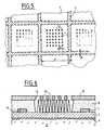
- la figure 5 est une vue schématique de dessus et partielle de la réalisation de la figure 4 ;
- la figure 6 est une vue schématique d'un autre mode de réalisation de l'invention ;
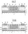
- la figure 7 est une vue schématique d'un autre mode de réalisation de l'invention ;
- la figure 8 est une vue schématique d'un autre mode de réalisation de l'invention.
- FIG. 1, already described and relating to the prior art, schematically represents a source of electrons with emissive cathodes with microtips;
- FIG. 2, already described and relating to the prior art, schematically represents a sectional and partial view of an electron source with emissive cathodes with microtips;
- FIG. 3, already described and relating to the prior art, schematically represents an electron emitter in short circuit with a grid;
- Figure 4 is a schematic sectional and partial view of a first embodiment of an electron source according to the invention;
- Figure 5 is a schematic top view and partial of the embodiment of Figure 4;
- Figure 6 is a schematic view of another embodiment of the invention;
- Figure 7 is a schematic view of another embodiment of the invention;
- Figure 8 is a schematic view of another embodiment of the invention.
En référence aux figures 4 et 5, on décrit maintenant une source d'électrons conforme à l'invention. Dans cette réalisation, les conducteurs cathodiques 5 présentent une structure en treillis. Les mailles du treillis peuvent être de géométrie quelconque. Dans la réalisation représentée, les mailles du treillis sont carrées. Le pas de la maille p est, par exemple, d'environ 50 micromètres et la largeur d des pistes conductrices formant le treillis est par exemple d'environ 5 micromètres. Ces pistes conductrices sont de préférence métalliques, par exemple en Al, Mo, Cr, Nb ou autre. Un conducteur cathodique 5 présente une largeur de 400 micromètres, les conducteurs cathodiques étant séparés les uns des autres d'une distance égale à 50 micromètres environ. On comprend donc qu'une zone de croisement d'un conducteur cathodique 5 avec une grille 10 (de largeur égale à 300 micromètres) recouvre plusieurs mailles du treillis. Dans ces conditions, chaque zone de recouvrement d'un conducteur cathodique 5 avec une grille 10 comprend 48 mailles. Le non fonctionnement d'une maille dû à des courts-circuits entre la grille 10 et des micropointes ne perturbe l'ensemble que dans la proportion de 1/48, ce qui n'a pas d'effet notable.With reference to FIGS. 4 and 5, a source of electrons according to the invention will now be described. In this embodiment, the
Les micropointes 12 sont réunies dans les zones centrales des mailles et sont reliées au conducteur cathodique 5 par une couche résistive 7 en silicium dope par exemple. La distance a séparant chaque micropointe 12 peut être de 5 micromètres par exemple ; la distance r séparant les micropointes 12 des pistes conductrices du treillis formant un conducteur cathodique 5 doit être suffisante pour que la chute de tension dans la couche résistive 7, nominal, en fonctionnement produise l'effet d'homogénéisation précité. La couche résistive 7 en silicium dope étant d'environ 0,5 micromètre par exemple, cette distance r est au minimum de 5 micromètres pour une chute de tension comprise entre 5 et 10 V en fonctionnement nominal. Par exemple, la distance r est choisie égale à 10 micromètres.The
Chaque maille contient un nombre n de micropointes 12 avec
Dans l'exemple représenté, n égale 36.In the example shown, n equals 36.
Dans cette réalisation, la résistance d'accès du conducteur cathodique 5 à l'ensemble des micropointes 12 est peu dépendante de la dimension de la maille et du nombre de micropointes qu'elle contient. Elle dépend essentiellement de la résistivite et de l'épaisseur de la couche résistive 7. Pour une couche résistive en silicium, la résistivité p est de l'ordre de 3 10³ Ohmscm ; son épaisseur e est par exemple égale à 0,5 micromètre.In this embodiment, the access resistance of the
La résistance d'accès R peut être approximativement calculée à l'aide de la formule :
on trouve que R égale approximativement 10⁷ Ohms, ce qui est suffisant pour obtenir une chute de tension d'environ 10 V dans la couche résistive 7.The access resistance R can be roughly calculated using the formula:
we find that R equals approximately 10⁷ Ohms, which is sufficient to obtain a voltage drop of approximately 10 V in the
Dans ces conditions, en cas de court-circuit entre un émetteur 12 et la grille 10, le courant de fuite dans une maille est sensiblement égal à 10 microampères, ce qui est tolérable car il n'altère pas le fonctionnement de la source d'électrons.Under these conditions, in the event of a short circuit between a
Un procédé de réalisation d'un tel dispositif peut par exemple comporter les étapes suivantes :
- a) sur
un substrat isolant 2, par exemple en verre, recouvert une fine couche 4 (d'épaisseur 1000 Å) de SiO₂, on dépose, par exemple par pulvérisation cathodique une couche métallique (d'épaisseur 2000 Å) par exemple en Nb ; - b) on réalise, par exemple par photolithographie et gravure ionique réactive, une structure en treillis dans la couche métallique. Cette structure est donc réalisée sur toute la surface active la source d'électrons ;
- c) on dépose, par exemple par pulvérisation cathodique, une couche résistive de silicium dope (d'épaisseur 5000 Å) ;
- d) on grave, par exemple par photogravure et gravure ionique réactive, la couche résistive et la couche métallique de manière à former des colonnes conductrices (par exemple, de largeur égale à 400 micromètres et espacées de 50 micromètres entre-elles) ;
- e) on termine ensuite la source d'électrons par la réalisation d'une couche isolante, de la grille et des micropointes selon des étapes décrites par exemple dans le brevet français n° 2 593 953 déposé au nom du demandeur.
- a) on an insulating
substrate 2, for example made of glass, covered with a thin layer 4 (of thickness 1000 Å) of SiO₂, a metallic layer (of thickness 2000 Å), for example of Nb, is deposited, for example by sputtering ; - b) a lattice structure in the metal layer is produced, for example by photolithography and reactive ion etching. This structure is therefore produced over the entire active surface of the electron source;
- c) a resistive layer of doped silicon (of thickness 5000 Å) is deposited, for example by sputtering;
- d) the resistive layer and the metal layer are etched, for example by photogravure and reactive ion etching, so as to form conductive columns (for example, of width equal to 400 micrometers and spaced 50 micrometers apart);
- e) the electron source is then terminated by the production of an insulating layer, the grid and the microtips according to steps described for example in French patent No. 2,593,953 filed in the name of the applicant.
Conformément à l'invention, les micropointes ne sont réalisées qu'à l'intérieur des mailles. Un positionnement des micropointes par rapport aux mailles des conducteurs cathodiques est donc nécessaire avec une précision de l'ordre de ± 5 micromètres.In accordance with the invention, the microtips are only produced inside the meshes. A positioning of the microtips relative to the meshes of the cathode conductors is therefore necessary with an accuracy of the order of ± 5 micrometers.
Selon un autre mode de réalisation représenté schématiquement sur la figure 6, les conducteurs cathodiques 5 possédant une structure en treillis reposent sur une couche résistive 7. Dans cette configuration, une couche résistive 7 est donc intercalée entre le support isolant (plus particulièrement la couche 4) et chaque conducteur cathodique 5.According to another embodiment shown schematically in FIG. 6, the
Selon une variante de réalisation représentée en coupe sur la figure 7, ce ne sont plus les conducteurs cathodiques 5 qui possèdent une structure en treillis mais les grilles.According to an alternative embodiment shown in section in FIG. 7, it is no longer the
Selon un premier mode de réalisation, une seconde couche résistive 18, par exemple en silicium dopé d'une résistivité d'environ 10⁴ Ohmscm et d'épaisseur égale à 0,4 micromètre, repose sur la couche isolante 8. Elle est percée d'ouvertures 20 pour permettre le passage des micropointes 12.According to a first embodiment, a second
Les grilles 10a en forme de treillis à mailles carrées reposent sur la seconde couche résistive 18. Les micropointes 12 sont placées à l'intérieur de la zone centrale des mailles du treillis.The
Selon un second mode de réalisation, la seconde couche résistive 18 recouvre les grilles 10b qui reposent sur la couche isolante 8.According to a second embodiment, the second
Dans cette variante de réalisation, les grilles peuvent être en Nb et présentent une épaissseur de 0,2 micromètre. La largeur de chaque grille 10a ou 10b peut être de 5 micromètres pour un pas de maille de 50 micromètres.In this alternative embodiment, the grids can be made of Nb and have a thickness of 0.2 micrometer. The width of each
Que ce soit dans le premier ou le second mode de réalisation, la seconde couche résistive 18 a un rôle de protection contre les courts-circuits, la couche résistive 7 assurant la fonction d'homogénéïsation de l'émission électronique.Whether in the first or second embodiment, the second
Dans cette variante de réalisation, les couches résistives 7 peuvent être en silicium dopé ayant par exemple une résistivité de 10⁵ Ohmscm et une épaisseur de 0,1 micromètre. Les conducteurs cathodiques 5 peuvent être par exemple en I T O (oxyde d'indium dopé à l'étain).In this variant embodiment, the
Selon une autre variante de réalisation, représentée schématiquement en coupe sur la figure 8, les grilles et les conducteurs cathodiques possèdent une structure en treillis à mailles carrées. Les mailles des grilles et des conducteurs cathodiques sont alors superposées : les pistes conductrices formant les mailles des grilles et des conducteurs cathodiques sont en regard dans les zones de recouvrement.According to another alternative embodiment, shown diagrammatically in section in FIG. 8, the grids and the cathode conductors have a lattice structure with square meshes. The meshes of the grids and the cathode conductors are then superimposed: the conductive tracks forming the meshes of the grids and the cathode conductors are opposite in the overlap zones.
De même que précédemment, une seconde couche résistive 18 recouvre chaque grille 10b ou bien les grilles 10a peuvent aussi recouvrir la seconde couche résistive 10a.As previously, a second
En ce qui concerne les conducteurs cathodiques, ceux-ci peuvent être recouverts par la couche isolante 7 (conducteur cathodique référence 5b) ou bien la recouvrir (conducteur cathodique référence 5a).As regards the cathode conductors, these can be covered by the insulating layer 7 (
Quelle que soit la variante de réalisation retenue, une source d'électrons possédant des électrodes en forme de treillis permet de diminuer les risques de claquage tout en assurant une bonne homogénéïsation de l'émission électronique. La structure en treillis permet d'augmenter la résistance d'accès des micropointes aux conducteurs cathodiques sans pour autant augmenter l'épaisseur de la couche résistive.Whatever the variant of embodiment chosen, a source of electrons having lattice-shaped electrodes makes it possible to reduce the risks of breakdown while ensuring good homogenization of the electronic emission. The lattice structure makes it possible to increase the access resistance of the microtips to the cathode conductors without increasing the thickness of the resistive layer.
Claims (13)
- Electron source comprising on an insulating support (2, 4) a first series of parallel electrodes serving as cathode conductors (5) and carrying a plurality of microdots (12) made from an electron emitting material and a second series of parallel electrodes (10) serving as grids and which are elastically insulated from the cathode conductors (5) by an insulating layer (8) and forming an angle therewith, which defines the intersection zones of the cathode conductors (5) and the grids (10), the girds (10) and the insulating layer (8) having openings (14) respectively facing the microdots (12), a resistive coating (7, 18) placed at least between one of the series of electrodes and the insulating layer (8), characterized in that each of the electrodes (5, 10) of at least one of the series has a grating structure in contact with a resistive coating (7, 18).
- Electron source according to claim 1, characterized in that the size of a mesh of the grating is less than the size of an intersection zone.
- Electron source according to claim 2, characterized in that an intersection zone covers several grating meshes.
- Electron source according to claim 1, characterized in that the grating meshes are square.
- Electron source according to claim 1, characterized in that the cathode conductors (5) have a grating structure.
- Electron source according to claim 5, characterized in that the microdots (12) occupy the central regions of the grating meshes.
- Electron source according to claim 5, characterized in that each cathode conductor (5) is covered by a resistive coating (7).
- Electron source according to claim 5, characterized in that a resistive coating (7) is inserted between the insulating support (2, 4) and each cathode conductor (5).
- Electron source according to either of the claims 7 and 8, characterized in that the resistive coating (7) is of doped silicon.
- Electron source according to claim 1, characterized in that the grids (10) have a grating structure.
- Electron source according to claim 10, characterized in that each grid (10) is covered by a second resistive coating (18) with openings (20) facing the microdots (12).
- Electron source according to claim 10, characterized in that each grid (10) rests on a second resistive coating (18) having openings (20) facing the microdots (12).
- Electron source according to either of the claims 11 and 12, characterized in that the second resistive coating (18) is of doped silicon.
Applications Claiming Priority (2)
| Application Number | Priority Date | Filing Date | Title |
|---|---|---|---|
| FR9007347 | 1990-06-13 | ||
| FR9007347AFR2663462B1 (en) | 1990-06-13 | 1990-06-13 | SOURCE OF ELECTRON WITH EMISSIVE MICROPOINT CATHODES. |
Publications (2)
| Publication Number | Publication Date |
|---|---|
| EP0461990A1 EP0461990A1 (en) | 1991-12-18 |
| EP0461990B1true EP0461990B1 (en) | 1994-10-19 |
Family
ID=9397551
Family Applications (1)
| Application Number | Title | Priority Date | Filing Date |
|---|---|---|---|
| EP91401536AExpired - LifetimeEP0461990B1 (en) | 1990-06-13 | 1991-06-11 | Micropoint cathode electron source |
Country Status (7)
| Country | Link |
|---|---|
| US (1) | US5194780A (en) |
| EP (1) | EP0461990B1 (en) |
| JP (1) | JP2657984B2 (en) |
| KR (1) | KR100204327B1 (en) |
| DE (1) | DE69104653T2 (en) |
| FI (1) | FI912802A7 (en) |
| FR (1) | FR2663462B1 (en) |
Families Citing this family (163)
| Publication number | Priority date | Publication date | Assignee | Title |
|---|---|---|---|---|
| FR2669124B1 (en)* | 1990-11-08 | 1993-01-22 | Commissariat Energie Atomique | BISTABLE ELECTROOPTIC DEVICE, SCREEN COMPRISING SUCH A DEVICE AND METHOD FOR IMPLEMENTING THE SCREEN. |
| JP3054205B2 (en)* | 1991-02-20 | 2000-06-19 | 株式会社リコー | Electron-emitting device integrated substrate |
| US5536193A (en) | 1991-11-07 | 1996-07-16 | Microelectronics And Computer Technology Corporation | Method of making wide band gap field emitter |
| FR2687839B1 (en)* | 1992-02-26 | 1994-04-08 | Commissariat A Energie Atomique | ELECTRON SOURCE WITH MICROPOINT EMISSIVE CATHODES AND FIELD EMISSION-EXCITED CATHODOLUMINESCENCE VISUALIZATION DEVICE USING THE SOURCE. |
| US5449970A (en) | 1992-03-16 | 1995-09-12 | Microelectronics And Computer Technology Corporation | Diode structure flat panel display |
| US5686791A (en) | 1992-03-16 | 1997-11-11 | Microelectronics And Computer Technology Corp. | Amorphic diamond film flat field emission cathode |
| US6127773A (en) | 1992-03-16 | 2000-10-03 | Si Diamond Technology, Inc. | Amorphic diamond film flat field emission cathode |
| US5543684A (en) | 1992-03-16 | 1996-08-06 | Microelectronics And Computer Technology Corporation | Flat panel display based on diamond thin films |
| US5679043A (en) | 1992-03-16 | 1997-10-21 | Microelectronics And Computer Technology Corporation | Method of making a field emitter |
| US5675216A (en) | 1992-03-16 | 1997-10-07 | Microelectronics And Computer Technololgy Corp. | Amorphic diamond film flat field emission cathode |
| US5548185A (en)* | 1992-03-16 | 1996-08-20 | Microelectronics And Computer Technology Corporation | Triode structure flat panel display employing flat field emission cathode |
| US5763997A (en) | 1992-03-16 | 1998-06-09 | Si Diamond Technology, Inc. | Field emission display device |
| US5721472A (en)* | 1992-04-07 | 1998-02-24 | Micron Display Technology, Inc. | Identifying and disabling shorted electrodes in field emission display |
| US5459480A (en)* | 1992-04-07 | 1995-10-17 | Micron Display Technology, Inc. | Architecture for isolating display grid sections in a field emission display |
| US5424605A (en)* | 1992-04-10 | 1995-06-13 | Silicon Video Corporation | Self supporting flat video display |
| US5374868A (en)* | 1992-09-11 | 1994-12-20 | Micron Display Technology, Inc. | Method for formation of a trench accessible cold-cathode field emission device |
| US5717285A (en)* | 1993-03-17 | 1998-02-10 | Commissariat A L 'energie Atomique | Microtip display device having a current limiting layer and a charge avoiding layer |
| FR2702869B1 (en)* | 1993-03-17 | 1995-04-21 | Commissariat Energie Atomique | Microtip display device and method of manufacturing the device. |
| US6034480A (en)* | 1993-07-08 | 2000-03-07 | Micron Technology, Inc. | Identifying and disabling shorted electrodes in field emission display |
| US5909203A (en)* | 1993-07-08 | 1999-06-01 | Micron Technology, Inc. | Architecture for isolating display grids in a field emission display |
| FR2707795B1 (en)* | 1993-07-12 | 1995-08-11 | Commissariat Energie Atomique | Improvement to a manufacturing process of a microtip electron source. |
| US5564959A (en)* | 1993-09-08 | 1996-10-15 | Silicon Video Corporation | Use of charged-particle tracks in fabricating gated electron-emitting devices |
| US5559389A (en)* | 1993-09-08 | 1996-09-24 | Silicon Video Corporation | Electron-emitting devices having variously constituted electron-emissive elements, including cones or pedestals |
| US7025892B1 (en) | 1993-09-08 | 2006-04-11 | Candescent Technologies Corporation | Method for creating gated filament structures for field emission displays |
| US5462467A (en)* | 1993-09-08 | 1995-10-31 | Silicon Video Corporation | Fabrication of filamentary field-emission device, including self-aligned gate |
| JP2699827B2 (en)* | 1993-09-27 | 1998-01-19 | 双葉電子工業株式会社 | Field emission cathode device |
| JP2743794B2 (en)* | 1993-10-25 | 1998-04-22 | 双葉電子工業株式会社 | Field emission cathode and method of manufacturing field emission cathode |
| CA2172803A1 (en) | 1993-11-04 | 1995-05-11 | Nalin Kumar | Methods for fabricating flat panel display systems and components |
| US5786659A (en)* | 1993-11-29 | 1998-07-28 | Futaba Denshi Kogyo K.K. | Field emission type electron source |
| TW253971B (en)* | 1994-02-21 | 1995-08-11 | Futaba Denshi Kogyo Kk | Method for driving electron gun and cathode ray tube |
| US5442193A (en)* | 1994-02-22 | 1995-08-15 | Motorola | Microelectronic field emission device with breakdown inhibiting insulated gate electrode |
| JP2856672B2 (en)* | 1994-02-28 | 1999-02-10 | 三星電管株式會社 | Field electron emission device and method of manufacturing the same |
| FR2717304B1 (en)* | 1994-03-09 | 1996-04-05 | Commissariat Energie Atomique | Electron source with microtip emissive cathodes. |
| US5583393A (en)* | 1994-03-24 | 1996-12-10 | Fed Corporation | Selectively shaped field emission electron beam source, and phosphor array for use therewith |
| US5448131A (en)* | 1994-04-13 | 1995-09-05 | Texas Instruments Incorporated | Spacer for flat panel display |
| FR2719156B1 (en)* | 1994-04-25 | 1996-05-24 | Commissariat Energie Atomique | Source of microtip electrons, microtips having two parts. |
| US5538450A (en)* | 1994-04-29 | 1996-07-23 | Texas Instruments Incorporated | Method of forming a size-arrayed emitter matrix for use in a flat panel display |
| JPH0845445A (en)* | 1994-04-29 | 1996-02-16 | Texas Instr Inc <Ti> | Flat panel,display unit and its manufacture |
| KR950034365A (en)* | 1994-05-24 | 1995-12-28 | 윌리엄 이. 힐러 | Anode Plate of Flat Panel Display and Manufacturing Method Thereof |
| US5491376A (en)* | 1994-06-03 | 1996-02-13 | Texas Instruments Incorporated | Flat panel display anode plate having isolation grooves |
| US5453659A (en) | 1994-06-10 | 1995-09-26 | Texas Instruments Incorporated | Anode plate for flat panel display having integrated getter |
| US5607335A (en)* | 1994-06-29 | 1997-03-04 | Silicon Video Corporation | Fabrication of electron-emitting structures using charged-particle tracks and removal of emitter material |
| FR2722913B1 (en)* | 1994-07-21 | 1996-10-11 | Pixel Int Sa | MICROPOINT CATHODE FOR FLAT SCREEN |
| DE69513581T2 (en)* | 1994-08-01 | 2000-09-07 | Motorola, Inc. | Arc suppressor for a field emission device |
| FR2723799B1 (en)* | 1994-08-16 | 1996-09-20 | Commissariat Energie Atomique | METHOD FOR MANUFACTURING A MICROPOINT ELECTRON SOURCE |
| US5525857A (en)* | 1994-08-19 | 1996-06-11 | Texas Instruments Inc. | Low density, high porosity material as gate dielectric for field emission device |
| EP0707301A1 (en) | 1994-09-14 | 1996-04-17 | Texas Instruments Incorporated | Power management for a display device |
| JP2907024B2 (en)* | 1994-09-26 | 1999-06-21 | 関西日本電気株式会社 | Electron-emitting device |
| US6252569B1 (en)* | 1994-09-28 | 2001-06-26 | Texas Instruments Incorporated | Large field emission display (FED) made up of independently operated display sections integrated behind one common continuous large anode which displays one large image or multiple independent images |
| US5521660A (en)* | 1994-09-29 | 1996-05-28 | Texas Instruments Inc. | Multimedia field emission device portable projector |
| EP0706164A1 (en) | 1994-10-03 | 1996-04-10 | Texas Instruments Incorporated | Power management for display devices |
| US5528098A (en)* | 1994-10-06 | 1996-06-18 | Motorola | Redundant conductor electron source |
| US5502347A (en) | 1994-10-06 | 1996-03-26 | Motorola, Inc. | Electron source |
| US5669690A (en) | 1994-10-18 | 1997-09-23 | Texas Instruments Incorporated | Multimedia field emission device projection system |
| FR2726122B1 (en) | 1994-10-19 | 1996-11-22 | Commissariat Energie Atomique | METHOD FOR MANUFACTURING A MICROPOINT ELECTRON SOURCE |
| JPH10508147A (en)* | 1994-10-31 | 1998-08-04 | ハネウエル・インコーポレーテッド | Field emitter display |
| US5527651A (en)* | 1994-11-02 | 1996-06-18 | Texas Instruments Inc. | Field emission device light source for xerographic printing process |
| DE69517700T2 (en)* | 1994-11-04 | 2000-11-23 | Micron Technology, Inc. | ARMING PROCEDURE FOR EMISSION POINTS THROUGH OXYDATION AT LOW TEMPERATURE |
| FR2726689B1 (en) | 1994-11-08 | 1996-11-29 | Commissariat Energie Atomique | FIELD-EFFECT ELECTRON SOURCE AND MANUFACTURING METHOD THEREOF, APPLICATION TO CATHODOLUMINESCENCE VISUALIZATION DEVICES |
| FR2726688B1 (en) | 1994-11-08 | 1996-12-06 | Commissariat Energie Atomique | FIELD-EFFECT ELECTRON SOURCE AND MANUFACTURING METHOD THEREOF, APPLICATION TO CATHODOLUMINESCENCE VISUALIZATION DEVICES |
| US5569975A (en)* | 1994-11-18 | 1996-10-29 | Texas Instruments Incorporated | Cluster arrangement of field emission microtips |
| EP0713236A1 (en) | 1994-11-18 | 1996-05-22 | Texas Instruments Incorporated | Electron emission apparatus |
| US5557159A (en)* | 1994-11-18 | 1996-09-17 | Texas Instruments Incorporated | Field emission microtip clusters adjacent stripe conductors |
| US5536993A (en)* | 1994-11-18 | 1996-07-16 | Texas Instruments Incorporated | Clustered field emission microtips adjacent stripe conductors |
| US5541466A (en)* | 1994-11-18 | 1996-07-30 | Texas Instruments Incorporated | Cluster arrangement of field emission microtips on ballast layer |
| US5477284A (en) | 1994-12-15 | 1995-12-19 | Texas Instruments Incorporated | Dual mode overhead projection system using field emission device |
| US5542866A (en)* | 1994-12-27 | 1996-08-06 | Industrial Technology Research Institute | Field emission display provided with repair capability of defects |
| US5554828A (en)* | 1995-01-03 | 1996-09-10 | Texas Instruments Inc. | Integration of pen-based capability into a field emission device system |
| US6559818B1 (en) | 1995-01-24 | 2003-05-06 | Micron Technology, Inc. | Method of testing addressable emissive cathodes |
| US5751262A (en)* | 1995-01-24 | 1998-05-12 | Micron Display Technology, Inc. | Method and apparatus for testing emissive cathodes |
| JP2897671B2 (en)* | 1995-01-25 | 1999-05-31 | 日本電気株式会社 | Field emission cold cathode |
| JP3079352B2 (en)* | 1995-02-10 | 2000-08-21 | 双葉電子工業株式会社 | Vacuum hermetic element using NbN electrode |
| US5598057A (en) | 1995-03-13 | 1997-01-28 | Texas Instruments Incorporated | Reduction of the probability of interlevel oxide failures by minimization of lead overlap area through bus width reduction |
| US5578902A (en)* | 1995-03-13 | 1996-11-26 | Texas Instruments Inc. | Field emission display having modified anode stripe geometry |
| US5578896A (en)* | 1995-04-10 | 1996-11-26 | Industrial Technology Research Institute | Cold cathode field emission display and method for forming it |
| US5594297A (en)* | 1995-04-19 | 1997-01-14 | Texas Instruments Incorporated | Field emission device metallization including titanium tungsten and aluminum |
| US5601466A (en)* | 1995-04-19 | 1997-02-11 | Texas Instruments Incorporated | Method for fabricating field emission device metallization |
| US5760858A (en)* | 1995-04-21 | 1998-06-02 | Texas Instruments Incorporated | Field emission device panel backlight for liquid crystal displays |
| US5628659A (en)* | 1995-04-24 | 1997-05-13 | Microelectronics And Computer Corporation | Method of making a field emission electron source with random micro-tip structures |
| US6296740B1 (en) | 1995-04-24 | 2001-10-02 | Si Diamond Technology, Inc. | Pretreatment process for a surface texturing process |
| FR2733253B1 (en) | 1995-04-24 | 1997-06-13 | Commissariat Energie Atomique | DEVICE FOR DEPOSITING MATERIAL BY EVAPORATION ON LARGE SURFACE SUBSTRATES |
| US5657054A (en)* | 1995-04-26 | 1997-08-12 | Texas Instruments Incorporated | Determination of pen location on display apparatus using piezoelectric point elements |
| US5657053A (en)* | 1995-04-26 | 1997-08-12 | Texas Instruments Incorporated | Method for determining pen location on display apparatus using piezoelectric point elements |
| US5591352A (en)* | 1995-04-27 | 1997-01-07 | Industrial Technology Research Institute | High resolution cold cathode field emission display method |
| US5631518A (en)* | 1995-05-02 | 1997-05-20 | Motorola | Electron source having short-avoiding extraction electrode and method of making same |
| US5543691A (en)* | 1995-05-11 | 1996-08-06 | Raytheon Company | Field emission display with focus grid and method of operating same |
| US5633120A (en)* | 1995-05-22 | 1997-05-27 | Texas Instruments Inc. | Method for achieving anode stripe delineation from an interlevel dielectric etch in a field emission device |
| US5577943A (en)* | 1995-05-25 | 1996-11-26 | Texas Instruments Inc. | Method for fabricating a field emission device having black matrix SOG as an interlevel dielectric |
| US5608285A (en)* | 1995-05-25 | 1997-03-04 | Texas Instruments Incorporated | Black matrix sog as an interlevel dielectric in a field emission device |
| US5621272A (en)* | 1995-05-30 | 1997-04-15 | Texas Instruments Incorporated | Field emission device with over-etched gate dielectric |
| US5589728A (en)* | 1995-05-30 | 1996-12-31 | Texas Instruments Incorporated | Field emission device with lattice vacancy post-supported gate |
| US5686782A (en)* | 1995-05-30 | 1997-11-11 | Texas Instruments Incorporated | Field emission device with suspended gate |
| US5759078A (en)* | 1995-05-30 | 1998-06-02 | Texas Instruments Incorporated | Field emission device with close-packed microtip array |
| US5558554A (en)* | 1995-05-31 | 1996-09-24 | Texas Instruments Inc. | Method for fabricating a field emission device anode plate having multiple grooves between anode conductors |
| US5594305A (en)* | 1995-06-07 | 1997-01-14 | Texas Instruments Incorporated | Power supply for use with switched anode field emission display including energy recovery apparatus |
| US5666024A (en)* | 1995-06-23 | 1997-09-09 | Texas Instruments Incorporated | Low capacitance field emission device with circular microtip array |
| US5674407A (en)* | 1995-07-03 | 1997-10-07 | Texas Instruments Incorporated | Method for selective etching of flat panel display anode plate conductors |
| US5611719A (en)* | 1995-07-06 | 1997-03-18 | Texas Instruments Incorporated | Method for improving flat panel display anode plate phosphor efficiency |
| FR2736753B1 (en)* | 1995-07-10 | 1997-08-22 | Commissariat Energie Atomique | METHOD FOR DETERMINING THE OPTIMAL GEOMETRIC CHARACTERISTICS OF THE MESHES OF A MICROPOINT TRANSMISSION SOURCE AND MICROPOINT SOURCE STRUCTURES OBTAINED BY THIS PROCESS |
| EP0757341B1 (en)* | 1995-08-01 | 2003-06-04 | STMicroelectronics S.r.l. | Limiting and selfuniforming cathode currents through the microtips of a field emission flat panel display |
| FR2737927B1 (en)* | 1995-08-17 | 1997-09-12 | Commissariat Energie Atomique | METHOD AND DEVICE FOR FORMING HOLES IN A LAYER OF PHOTOSENSITIVE MATERIAL, PARTICULARLY FOR THE MANUFACTURE OF ELECTRON SOURCES |
| FR2737928B1 (en)* | 1995-08-17 | 1997-09-12 | Commissariat Energie Atomique | DEVICE FOR INSOLATING MICROMETRIC AND / OR SUBMICROMETRIC ZONES IN A PHOTOSENSITIVE LAYER AND METHOD FOR PRODUCING PATTERNS IN SUCH A LAYER |
| US5635791A (en)* | 1995-08-24 | 1997-06-03 | Texas Instruments Incorporated | Field emission device with circular microtip array |
| US5606225A (en)* | 1995-08-30 | 1997-02-25 | Texas Instruments Incorporated | Tetrode arrangement for color field emission flat panel display with barrier electrodes on the anode plate |
| US5628662A (en)* | 1995-08-30 | 1997-05-13 | Texas Instruments Incorporated | Method of fabricating a color field emission flat panel display tetrode |
| US5763998A (en)* | 1995-09-14 | 1998-06-09 | Chorus Corporation | Field emission display arrangement with improved vacuum control |
| CN1202974A (en) | 1995-10-26 | 1998-12-23 | 图象技术公司 | Cold cathode field emitter flat screen display |
| US5818165A (en)* | 1995-10-27 | 1998-10-06 | Texas Instruments Incorporated | Flexible fed display |
| US5672933A (en)* | 1995-10-30 | 1997-09-30 | Texas Instruments Incorporated | Column-to-column isolation in fed display |
| US5767619A (en)* | 1995-12-15 | 1998-06-16 | Industrial Technology Research Institute | Cold cathode field emission display and method for forming it |
| US6031250A (en)* | 1995-12-20 | 2000-02-29 | Advanced Technology Materials, Inc. | Integrated circuit devices and methods employing amorphous silicon carbide resistor materials |
| US6252347B1 (en) | 1996-01-16 | 2001-06-26 | Raytheon Company | Field emission display with suspended focusing conductive sheet |
| US5952987A (en)* | 1996-01-18 | 1999-09-14 | Micron Technology, Inc. | Method and apparatus for improved gray scale control in field emission displays |
| JPH09219144A (en)* | 1996-02-08 | 1997-08-19 | Futaba Corp | Electric field emitting cathode and its manufacture |
| US5593562A (en)* | 1996-02-20 | 1997-01-14 | Texas Instruments Incorporated | Method for improving flat panel display anode plate phosphor efficiency |
| US5733160A (en)* | 1996-03-01 | 1998-03-31 | Texas Instruments Incorporated | Method of forming spacers for a flat display apparatus |
| US5944975A (en)* | 1996-03-26 | 1999-08-31 | Texas Instruments Incorporated | Method of forming a lift-off layer having controlled adhesion strength |
| US5684356A (en)* | 1996-03-29 | 1997-11-04 | Texas Instruments Incorporated | Hydrogen-rich, low dielectric constant gate insulator for field emission device |
| US5830527A (en)* | 1996-05-29 | 1998-11-03 | Texas Instruments Incorporated | Flat panel display anode structure and method of making |
| US5865659A (en)* | 1996-06-07 | 1999-02-02 | Candescent Technologies Corporation | Fabrication of gated electron-emitting device utilizing distributed particles to define gate openings and utilizing spacer material to control spacing between gate layer and electron-emissive elements |
| US6187603B1 (en) | 1996-06-07 | 2001-02-13 | Candescent Technologies Corporation | Fabrication of gated electron-emitting devices utilizing distributed particles to define gate openings, typically in combination with lift-off of excess emitter material |
| US5865657A (en)* | 1996-06-07 | 1999-02-02 | Candescent Technologies Corporation | Fabrication of gated electron-emitting device utilizing distributed particles to form gate openings typically beveled and/or combined with lift-off or electrochemical removal of excess emitter material |
| US5755944A (en)* | 1996-06-07 | 1998-05-26 | Candescent Technologies Corporation | Formation of layer having openings produced by utilizing particles deposited under influence of electric field |
| US5811926A (en)* | 1996-06-18 | 1998-09-22 | Ppg Industries, Inc. | Spacer units, image display panels and methods for making and using the same |
| US5834891A (en)* | 1996-06-18 | 1998-11-10 | Ppg Industries, Inc. | Spacers, spacer units, image display panels and methods for making and using the same |
| US5791961A (en)* | 1996-06-21 | 1998-08-11 | Industrial Technology Research Institute | Uniform field emission device |
| JP2970539B2 (en)* | 1996-06-27 | 1999-11-02 | 日本電気株式会社 | Field emission cathode and cathode ray tube using the same |
| FR2751785A1 (en)* | 1996-07-29 | 1998-01-30 | Commissariat Energie Atomique | METHOD AND DEVICE FOR FORMING PATTERNS IN A PHOTOSENSITIVE RESIN LAYER BY CONTINUOUS LASER INSOLATION, APPLICATION TO THE MANUFACTURE OF EMISSIVE MICROPOINT CATHODE ELECTRON SOURCES AND FLAT SCREENS |
| EP0834897B1 (en) | 1996-10-04 | 2002-05-02 | STMicroelectronics S.r.l. | Method of fabricating flat field emission display screens and flat screen obtained thereby |
| US5719406A (en)* | 1996-10-08 | 1998-02-17 | Motorola, Inc. | Field emission device having a charge bleed-off barrier |
| US5821680A (en)* | 1996-10-17 | 1998-10-13 | Sandia Corporation | Multi-layer carbon-based coatings for field emission |
| US5760535A (en)* | 1996-10-31 | 1998-06-02 | Motorola, Inc. | Field emission device |
| US6081246A (en) | 1996-11-12 | 2000-06-27 | Micron Technology, Inc. | Method and apparatus for adjustment of FED image |
| US5836799A (en)* | 1996-12-06 | 1998-11-17 | Texas Instruments Incorporated | Self-aligned method of micro-machining field emission display microtips |
| JP3156755B2 (en)* | 1996-12-16 | 2001-04-16 | 日本電気株式会社 | Field emission cold cathode device |
| US5780960A (en)* | 1996-12-18 | 1998-07-14 | Texas Instruments Incorporated | Micro-machined field emission microtips |
| US5938493A (en)* | 1996-12-18 | 1999-08-17 | Texas Instruments Incorporated | Method for increasing field emission tip efficiency through micro-milling techniques |
| US5828163A (en)* | 1997-01-13 | 1998-10-27 | Fed Corporation | Field emitter device with a current limiter structure |
| JP3764906B2 (en)* | 1997-03-11 | 2006-04-12 | 独立行政法人産業技術総合研究所 | Field emission cathode |
| JPH10340666A (en)* | 1997-06-09 | 1998-12-22 | Futaba Corp | Field electron emission element |
| US6013986A (en)* | 1997-06-30 | 2000-01-11 | Candescent Technologies Corporation | Electron-emitting device having multi-layer resistor |
| US6147664A (en)* | 1997-08-29 | 2000-11-14 | Candescent Technologies Corporation | Controlling the brightness of an FED device using PWM on the row side and AM on the column side |
| FR2769114B1 (en)* | 1997-09-30 | 1999-12-17 | Pixtech Sa | SIMPLIFICATION OF THE ADDRESSING OF A MICROPOINT SCREEN |
| US6144144A (en)* | 1997-10-31 | 2000-11-07 | Candescent Technologies Corporation | Patterned resistor suitable for electron-emitting device |
| US5910792A (en)* | 1997-11-12 | 1999-06-08 | Candescent Technologies, Corp. | Method and apparatus for brightness control in a field emission display |
| JP3353818B2 (en)* | 1998-03-26 | 2002-12-03 | 日本電気株式会社 | Field emission cold cathode device |
| US6710538B1 (en)* | 1998-08-26 | 2004-03-23 | Micron Technology, Inc. | Field emission display having reduced power requirements and method |
| US6417627B1 (en)* | 1999-02-03 | 2002-07-09 | Micron Technology, Inc. | Matrix-addressable display with minimum column-row overlap and maximum metal line-width |
| KR100385322B1 (en)* | 1999-11-27 | 2003-05-23 | 새천년 태양 주식회사 | A method for preparing healthy alcohol using medicinal herbs |
| KR20020008727A (en)* | 2000-07-25 | 2002-01-31 | 유종근 | Health Drink of Hobakdaebocha Using the Pumpkin and Medicinal Herbs and Manufacturing Method Thereof |
| KR20020008729A (en)* | 2000-07-25 | 2002-01-31 | 유종근 | Health Drink of Hobakpalbocha Using the Pumpkin and Medicinal Herbs and Manufacturing Method Thereof |
| JP2002334670A (en)* | 2001-05-09 | 2002-11-22 | Hitachi Ltd | Display device |
| JP2003249182A (en)* | 2002-02-22 | 2003-09-05 | Hitachi Ltd | Display device |
| KR100852690B1 (en)* | 2002-04-22 | 2008-08-19 | 삼성에스디아이 주식회사 | Carbon nanotube emitter paste composition for field emission display device and manufacturing method of carbon nanotube emitter for field emission display device using same |
| US20040245224A1 (en)* | 2003-05-09 | 2004-12-09 | Nano-Proprietary, Inc. | Nanospot welder and method |
| KR20050087376A (en)* | 2004-02-26 | 2005-08-31 | 삼성에스디아이 주식회사 | Emitter composition of flat panel display and carbon emitter using the same |
| JP2005340133A (en)* | 2004-05-31 | 2005-12-08 | Sony Corp | Cathode panel treating method, as well as cold-cathode field electron emission display device, and its manufacturing method |
| US20080020499A1 (en)* | 2004-09-10 | 2008-01-24 | Dong-Wook Kim | Nanotube assembly including protective layer and method for making the same |
| US7868850B2 (en)* | 2004-10-06 | 2011-01-11 | Samsung Electronics Co., Ltd. | Field emitter array with split gates and method for operating the same |
| TWI272870B (en)* | 2005-11-18 | 2007-02-01 | Tatung Co | Field emission display device |
| KR20080075360A (en)* | 2007-02-12 | 2008-08-18 | 삼성에스디아이 주식회사 | Light emitting device and display device using same |
| US8260174B2 (en) | 2008-06-30 | 2012-09-04 | Xerox Corporation | Micro-tip array as a charging device including a system of interconnected air flow channels |
| US9053890B2 (en) | 2013-08-02 | 2015-06-09 | University Health Network | Nanostructure field emission cathode structure and method for making |
Family Cites Families (11)
| Publication number | Priority date | Publication date | Assignee | Title |
|---|---|---|---|---|
| US3735183A (en)* | 1971-05-19 | 1973-05-22 | Ferranti Ltd | Gaseous discharge display device with a layer of electrically resistive material |
| JPS5325632B2 (en)* | 1973-03-22 | 1978-07-27 | ||
| US4020381A (en)* | 1974-12-09 | 1977-04-26 | Texas Instruments Incorporated | Cathode structure for a multibeam cathode ray tube |
| US4098536A (en)* | 1976-11-24 | 1978-07-04 | Mills Marion T | Weathershield for golf carts |
| DE3243596C2 (en)* | 1982-11-25 | 1985-09-26 | M.A.N. Maschinenfabrik Augsburg-Nürnberg AG, 8000 München | Method and device for transferring images to a screen |
| FR2593953B1 (en)* | 1986-01-24 | 1988-04-29 | Commissariat Energie Atomique | METHOD FOR MANUFACTURING A DEVICE FOR VIEWING BY CATHODOLUMINESCENCE EXCITED BY FIELD EMISSION |
| US4721885A (en)* | 1987-02-11 | 1988-01-26 | Sri International | Very high speed integrated microelectronic tubes |
| FR2617534A1 (en)* | 1987-06-30 | 1989-01-06 | Inst Francais Du Petrole | DEVICE FOR PUMPING A FLUID INTO THE BOTTOM OF A WELL |
| JP2607251B2 (en)* | 1987-08-26 | 1997-05-07 | 松下電工株式会社 | Field emission cathode |
| FR2623013A1 (en)* | 1987-11-06 | 1989-05-12 | Commissariat Energie Atomique | ELECTRO SOURCE WITH EMISSIVE MICROPOINT CATHODES AND FIELD EMISSION-INDUCED CATHODOLUMINESCENCE VISUALIZATION DEVICE USING THE SOURCE |
| US5075591A (en)* | 1990-07-13 | 1991-12-24 | Coloray Display Corporation | Matrix addressing arrangement for a flat panel display with field emission cathodes |
- 1990
- 1990-06-13FRFR9007347Apatent/FR2663462B1/ennot_activeExpired - Lifetime
- 1991
- 1991-05-31USUS07/703,684patent/US5194780A/ennot_activeExpired - Lifetime
- 1991-06-10KRKR1019910009509Apatent/KR100204327B1/ennot_activeExpired - Fee Related
- 1991-06-11JPJP13895991Apatent/JP2657984B2/ennot_activeExpired - Lifetime
- 1991-06-11EPEP91401536Apatent/EP0461990B1/ennot_activeExpired - Lifetime
- 1991-06-11DEDE69104653Tpatent/DE69104653T2/ennot_activeExpired - Lifetime
- 1991-06-11FIFI912802Apatent/FI912802A7/ennot_activeApplication Discontinuation
Also Published As
| Publication number | Publication date |
|---|---|
| FI912802L (en) | 1991-12-14 |
| DE69104653T2 (en) | 1995-05-04 |
| FR2663462A1 (en) | 1991-12-20 |
| JP2657984B2 (en) | 1997-09-30 |
| FR2663462B1 (en) | 1992-09-11 |
| US5194780A (en) | 1993-03-16 |
| DE69104653D1 (en) | 1994-11-24 |
| FI912802A0 (en) | 1991-06-11 |
| FI912802A7 (en) | 1991-12-14 |
| KR920001744A (en) | 1992-01-30 |
| EP0461990A1 (en) | 1991-12-18 |
| JPH04229922A (en) | 1992-08-19 |
| KR100204327B1 (en) | 1999-07-01 |
Similar Documents
| Publication | Publication Date | Title |
|---|---|---|
| EP0461990B1 (en) | Micropoint cathode electron source | |
| EP0316214B1 (en) | Electron source comprising emissive cathodes with microtips, and display device working by cathodoluminescence excited by field emission using this source | |
| EP0558393B1 (en) | Micropoint cathode electron source and display device with cathodo-luminescence excited by field emission using same source | |
| EP0234989B1 (en) | Method of manufacturing an imaging device using field emission cathodoluminescence | |
| EP0267824B1 (en) | Transistor-driven electro-optical visualization screen, and method of manufacturing it | |
| EP1885649A2 (en) | Method for making an emissive cathode | |
| FR2710781A1 (en) | Device forming a field-emission cathode | |
| EP1826797B1 (en) | Nanotube cathode structure for emissive screen | |
| FR2707795A1 (en) | Improvement to a method of manufacturing a microtip electron source. | |
| FR2742578A1 (en) | Manufacturing field emission cathode | |
| EP1139374A1 (en) | Cathode plate of a flat viewing screen | |
| EP0671755B1 (en) | Electron source comprising emissive cathodes with microtips | |
| EP0734042B1 (en) | Anode of a flat viewing screen with resistive strips | |
| EP0616356B1 (en) | Micropoint display device and method of fabrication | |
| EP0708473B1 (en) | Manufacturing method for micropoint electron source | |
| EP0625277B1 (en) | Flat screen having individually dipole-protected microdots | |
| EP0806788A1 (en) | Anode of a flat display screen with protection ring | |
| EP1210721B1 (en) | Field emission flat screen with modulating electrode | |
| EP0884753A1 (en) | Method for making spacers for a flat panel display | |
| EP0877407A1 (en) | Anode of a flat display screen | |
| FR2790329A1 (en) | RESISTIVE FLAT SCREEN ANODE | |
| US5903100A (en) | Reduction of smearing in cold cathode displays | |
| EP0867908A1 (en) | Uniforming the potential electron emission 0f a cathode of a flat screen with microtips | |
| WO2000021112A1 (en) | Electron source comprising at least a protective electrode against spurious emissions | |
| WO2008074825A1 (en) | Cathode structure for a flat screen with refocusing grid |
Legal Events
| Date | Code | Title | Description |
|---|---|---|---|
| PUAI | Public reference made under article 153(3) epc to a published international application that has entered the european phase | Free format text:ORIGINAL CODE: 0009012 | |
| AK | Designated contracting states | Kind code of ref document:A1 Designated state(s):CH DE GB IT LI NL SE | |
| 17P | Request for examination filed | Effective date:19920516 | |
| 17Q | First examination report despatched | Effective date:19931221 | |
| GRAA | (expected) grant | Free format text:ORIGINAL CODE: 0009210 | |
| AK | Designated contracting states | Kind code of ref document:B1 Designated state(s):CH DE GB IT LI NL SE | |
| REF | Corresponds to: | Ref document number:69104653 Country of ref document:DE Date of ref document:19941124 | |
| ITF | It: translation for a ep patent filed | ||
| EAL | Se: european patent in force in sweden | Ref document number:91401536.7 | |
| GBT | Gb: translation of ep patent filed (gb section 77(6)(a)/1977) | Effective date:19950111 | |
| PLBE | No opposition filed within time limit | Free format text:ORIGINAL CODE: 0009261 | |
| STAA | Information on the status of an ep patent application or granted ep patent | Free format text:STATUS: NO OPPOSITION FILED WITHIN TIME LIMIT | |
| 26N | No opposition filed | ||
| PGFP | Annual fee paid to national office [announced via postgrant information from national office to epo] | Ref country code:SE Payment date:19960529 Year of fee payment:6 | |
| PGFP | Annual fee paid to national office [announced via postgrant information from national office to epo] | Ref country code:CH Payment date:19970610 Year of fee payment:7 | |
| PG25 | Lapsed in a contracting state [announced via postgrant information from national office to epo] | Ref country code:SE Effective date:19970612 | |
| PGFP | Annual fee paid to national office [announced via postgrant information from national office to epo] | Ref country code:NL Payment date:19970626 Year of fee payment:7 | |
| EUG | Se: european patent has lapsed | Ref document number:91401536.7 | |
| PG25 | Lapsed in a contracting state [announced via postgrant information from national office to epo] | Ref country code:LI Free format text:LAPSE BECAUSE OF NON-PAYMENT OF DUE FEES Effective date:19980630 Ref country code:CH Free format text:LAPSE BECAUSE OF NON-PAYMENT OF DUE FEES Effective date:19980630 | |
| PG25 | Lapsed in a contracting state [announced via postgrant information from national office to epo] | Ref country code:NL Free format text:LAPSE BECAUSE OF NON-PAYMENT OF DUE FEES Effective date:19990101 | |
| REG | Reference to a national code | Ref country code:CH Ref legal event code:PL | |
| NLV4 | Nl: lapsed or anulled due to non-payment of the annual fee | Effective date:19990101 | |
| REG | Reference to a national code | Ref country code:GB Ref legal event code:IF02 | |
| PGFP | Annual fee paid to national office [announced via postgrant information from national office to epo] | Ref country code:IT Payment date:20100625 Year of fee payment:20 | |
| PGFP | Annual fee paid to national office [announced via postgrant information from national office to epo] | Ref country code:GB Payment date:20100618 Year of fee payment:20 Ref country code:DE Payment date:20100625 Year of fee payment:20 | |
| REG | Reference to a national code | Ref country code:DE Ref legal event code:R071 Ref document number:69104653 Country of ref document:DE | |
| REG | Reference to a national code | Ref country code:DE Ref legal event code:R071 Ref document number:69104653 Country of ref document:DE | |
| REG | Reference to a national code | Ref country code:GB Ref legal event code:PE20 Expiry date:20110610 | |
| PG25 | Lapsed in a contracting state [announced via postgrant information from national office to epo] | Ref country code:GB Free format text:LAPSE BECAUSE OF EXPIRATION OF PROTECTION Effective date:20110610 | |
| PG25 | Lapsed in a contracting state [announced via postgrant information from national office to epo] | Ref country code:DE Free format text:LAPSE BECAUSE OF EXPIRATION OF PROTECTION Effective date:20110612 |