EP0461926B1 - Multilevel inclusion in multilevel cache hierarchies - Google Patents
Multilevel inclusion in multilevel cache hierarchiesDownload PDFInfo
- Publication number
- EP0461926B1 EP0461926B1EP91305422AEP91305422AEP0461926B1EP 0461926 B1EP0461926 B1EP 0461926B1EP 91305422 AEP91305422 AEP 91305422AEP 91305422 AEP91305422 AEP 91305422AEP 0461926 B1EP0461926 B1EP 0461926B1
- Authority
- EP
- European Patent Office
- Prior art keywords
- level cache
- cache
- way
- data
- controller
- Prior art date
- Legal status (The legal status is an assumption and is not a legal conclusion. Google has not performed a legal analysis and makes no representation as to the accuracy of the status listed.)
- Expired - Lifetime
Links
Images


Classifications
- G—PHYSICS
- G06—COMPUTING OR CALCULATING; COUNTING
- G06F—ELECTRIC DIGITAL DATA PROCESSING
- G06F12/00—Accessing, addressing or allocating within memory systems or architectures
- G06F12/02—Addressing or allocation; Relocation
- G06F12/08—Addressing or allocation; Relocation in hierarchically structured memory systems, e.g. virtual memory systems
- G06F12/0802—Addressing of a memory level in which the access to the desired data or data block requires associative addressing means, e.g. caches
- G06F12/0806—Multiuser, multiprocessor or multiprocessing cache systems
- G06F12/0811—Multiuser, multiprocessor or multiprocessing cache systems with multilevel cache hierarchies
- G—PHYSICS
- G06—COMPUTING OR CALCULATING; COUNTING
- G06F—ELECTRIC DIGITAL DATA PROCESSING
- G06F12/00—Accessing, addressing or allocating within memory systems or architectures
- G06F12/02—Addressing or allocation; Relocation
- G06F12/08—Addressing or allocation; Relocation in hierarchically structured memory systems, e.g. virtual memory systems
- G06F12/0802—Addressing of a memory level in which the access to the desired data or data block requires associative addressing means, e.g. caches
- G06F12/0806—Multiuser, multiprocessor or multiprocessing cache systems
- G06F12/0815—Cache consistency protocols
- G06F12/0831—Cache consistency protocols using a bus scheme, e.g. with bus monitoring or watching means
Definitions
- the present inventionrelates to microprocessor cache subsystems in computer systems, and more specifically to a method and apparatus for achieving multilevel inclusion among first level and second level caches in a computer system so that the second level cache controller can perform the principal snooping responsibilities for both caches.
- the personal computer industryis a vibrant and growing field that continues to evolve as new innovations occur.
- the driving force behind this innovationhas been the increasing demand for faster and more powerful computers.
- a major bottleneck in personal computer speedhas historically been the speed with which data can be accessed from memory, referred to as the memory access time.
- the microprocessorwith its relatively fast processor cycle times, has generally been delayed by the use of wait states during memory accesses to account for the relatively slow memory access times. Therefore, improvement in memory access times has been one of the major areas of research in enhancing computer performance.
- a cacheis a small amount of very fast, and expensive, zero wait state memory that is used to store a copy of frequently accessed code and data from main memory.
- the microprocessorcan operate out of this very fast memory and thereby reduce the number of wait states that must be interposed during memory accesses.
- a cache read hittakes place, and the data from the memory access can be returned to the processor from the cache without incurring wait states.
- a cache read misstakes place, and the memory request is forwarded to the system and the data is retrieved from main memory, as would normally be done if the cache did not exist.
- the data that is retrieved from memoryis provided to the processor and is also written into the cache due to the statistical likelihood that this data will be requested again by the processor.
- An efficient cacheyields a high "hit rate”, which is the percentage of cache hits that occur during all memory accesses.
- hit rateis the percentage of cache hits that occur during all memory accesses.
- the majority of memory accessesare serviced with zero wait states.
- the net effect of a high cache hit rateis that the wait states incurred on a relatively infrequent miss are averaged over a large number of zero wait state cache hit accesses, resulting in an average of nearly zero wait states per access.
- cache hitsare serviced locally without requiring use of the system bus. Therefore, a processor operating out of its local cache has a much lower "bus utilization.” This reduces system bus bandwidth used by the processor, making more bandwidth available for other bus masters.
- cachesAnother important feature of caches is that the processor can operate out of its local cache when it does not have control of the system bus, thereby increasing the efficiency of the computer system. In systems without microprocessor caches, the processor generally must remain idle while it does not have control of the system bus. This reduces the overall efficiency of the computer system because the processor cannot do any useful work at this time. However, if the processor includes a cache placed on its local bus, it can retrieve the necessary code and data from its cache to perform useful work while other devices have control of the system bus, thereby increasing system efficiency.
- Cache performanceis dependent on many factors, including the hit rate and the cache memory access time.
- the hit rateis a measure of how efficient a cache is in maintaining a copy of the most frequently used code and data, and, to a large extent, it is a function of the size of the cache.
- a larger cachewill generally have a higher hit rate than a smaller cache.
- Increasing the size of the cachecan possibly degrade the cache memory access time.
- cache designs for a larger cachecan be achieved using cache memory with the fastest possible access times such that the limiting factor in the design is the minimum CPU access time. In this way, a larger cache would not be penalized by a possibly slower cache memory access time with respect to the memory access time of a smaller cache because the limiting factor in the design would be the minimum CPU access time.
- a cachecan generally be organized into either a direct-mapped or set-associative configuration.
- the physical address space of the computeris conceptually divided up into a number of equal pages, with the page size equaling the size of the cache.
- the cacheis divided up into a number of sets, with each set having a certain number of lines.
- Each of the pages in main memoryhas a number of lines equivalent to the number of lines in the cache, and each line from a respective page in main memory corresponds to a similarly located line in the cache.
- each memory line from a page in main memoryreferred to as a page offset
- a page offsetcan only reside in the equivalently located line or page offset in the cache. Due to this restriction, the cache only need refer to a certain number of the upper address bits of a memory address, referred to as a tag, to determine if a copy of the data from the respective memory address resides in the cache because the lower order address bits are pre-determined by the page offset of the memory address.
- a direct-mapped cacheis organized as one bank of memory that is equivalent in size to a conceptual page in main memory
- a set-associative cacheincludes a number of banks, or ways, of memory that are each equivalent in size to a conceptual page in main memory. Accordingly, a page offset in main memory can be mapped to a number of locations in the cache equal to the number of ways in the cache. For example, in a 4-way set associative cache, a line or page offset from main memory can reside in the equivalent page offset location in any of the four ways of the cache.
- a set-associative cachegenerally includes a replacement algorithm that determines which bank, or way, with which to fill data when a read miss occurs.
- Many set-associative cachesuse some form of a least recently used (LRU) algorithm that places new data in the way that was least recently accessed. This is because, statistically, the way most recently used or accessed to provide data to the processor is the one most likely to be needed again in the future. Therefore, the LRU algorithm ensures that the block which is replaced is the least likely to have data requested by the cache.
- LRUleast recently used
- Cache managementis generally performed by a device referred to as a cache controller.
- the cache controllerincludes a directory that holds an associated entry for each set in the cache. This entry generally has three components: a tag, a tag valid bit, and a number of line valid bits equaling the number of lines in each cache set.
- the tagacts as a main memory page number, and it holds the upper address bits of the particular page in main memory from which the copy of data residing in the respective set of the cache originated.
- the status of the tag valid bitdetermines whether the data in the respective set of the cache is considered valid or invalid. If the tag valid bit is clear, then the entire set is considered invalid. If the tag valid bit is true, then an individual line within the set is considered valid or invalid depending on the status of its respective line valid bit.
- a principal cache management policyis the preservation of cache coherency.
- Cache coherencyrefers to the requirement that any copy of data in a cache must be identical to (or actually be) the owner of that location's data.
- the owner of a location's datais generally defined as the respective location having the most recent version of the data residing in the respective memory location.
- the owner of datacan be either an unmodified location in main memory, or a modified location in a write-back cache.
- a bus mastersuch as a direct memory access controller, network or disk interface card, or video graphics card, might alter the contents of a main memory location that is duplicated in the cache. When this occurs, the cache is said to hold "stale" or invalid data.
- the cache controllerIn order to maintain cache coherency, it is necessary for the cache controller to monitor the system bus when the processor does not own the system bus to see if another bus master accesses main memory. This method of monitoring the bus is referred to as snooping.
- the cache controllermust monitor the system bus during memory reads by a bus master in a write-back cache design because of the possibility that a previous processor write may have altered a copy of data in the cache that has not been updated in main memory. This is referred to as read snooping. On a read snoop hit where the cache contains data not yet updated in main memory, the cache controller generally provides the respective data to main memory, and the requesting bus master generally reads this data en route from the cache controller to main memory, this operation being referred to as snarfing. The cache controller must also monitor the system bus during memory writes because the bus master may write to or alter a memory location that resides in the cache. This is referred to as write snooping.
- the cache entryOn a write snoop hit, the cache entry is either marked invalid in the cache directory by the cache controller, signifying that this entry is no longer correct, or the cache is updated along with main memory. Therefore, when a bus master reads or writes to main memory in a write-back cache design, or writes to main memory in a write-through cache design, the cache controller must latch the system address and perform a cache look-up in the tag directory corresponding to the page offset location where the memory access occurred to see if the main memory location being accessed also resides in the cache. If a copy of the data from this location does reside in the cache, then the cache controller takes the appropriate action depending on whether a read or write snoop hit has occurred. This prevents incompatible data from being stored in main memory and the cache, thereby preserving cache coherency.
- processor writes to memoryAnother consideration in the preservation of cache coherency is the handling of processor writes to memory.
- the memory locationWhen the processor writes to main memory, the memory location must be checked to determine if a copy of the data from this location also resides in the cache. If a processor write hit occurs in a write-back cache design, then the cache location is updated with the new data and main memory may be updated with the new data at a later time or should the need arise.
- the main memory locationis generally updated in conjunction with the cache location on a processor write hit. If a processor write miss occurs, the cache controller may ignore the write miss in a write-through cache design because the cache is unaffected in this design.
- the cache controllermay perform a "write-allocate" whereby the cache controller allocates a new line in the cache in addition to passing the data the data to the main memory.
- the cache controllerIn a write-back cache design, the cache controller generally allocates a new line in the cache when a processor write miss occurs. This generally involves reading the remaining entries to fill the line from main memory before or jointly with providing the write data to the cache. Main memory is updated at a later time should the need arise.
- Cacheshave generally been designed independently of the microprocessor.
- the cacheis placed on the local bus of the microprocessor and interfaced between the processor and the system bus during the design of the computer system.
- many processorsare currently being designed with an on-chip cache in order to meet performance goals with regard to memory access times.
- the on-chip cache used in these processorsis generally small, an exemplary size being 8 kbytes in size.
- the smaller, on-chip cacheis generally faster than a large off-chip cache and reduces the gap between fast processor cycle times and the relatively slow access times of large caches.
- an external, second level cacheis often added to the system to further improve memory access time.
- the second level cacheis generally much larger than the on-chip cache, and, when used in conjunction with the on-chip cache, provides a greater overall hit rate than the on-chip cache would provide by itself.
- the on-chip or first level cacheis first checked to see if a copy of the data resides there. If so, then a first level cache hit occurs, and the first level cache provides the appropriate data to the processor. If a first level cache miss occurs, then the second level cache is then checked. If a second level cache hit occurs, then the data is provided from the second level cache to the processor. If a second level cache miss occurs, then the data is retrieved from main memory. Write operations are similar, with mix and matching of the operations discussed above being possible.
- Multilevel inclusionprovides that the second level cache is guaranteed to have a copy of what is inside the first level, or on-chip cache. When this occurs, the second level cache is said to hold a superset of the first level cache. Multilevel inclusion has mostly been used in multi-processor systems to prevent cache coherency problems. When multilevel inclusion is implemented in multi-processor systems, the higher level caches can shield the lower level caches from cache coherency problems and thereby prevent unnecessary blind checks and invalidations that would otherwise occur in the lower level caches if multilevel inclusion were not implemented.
- Multilevel cache hierarchies with multilevel inclusionare for example disclosed in Journal of Parallel and Distributed Computing, vol 6, no. 3, June 1989, DULUTH, MN, US, pages 451-476, BAER et AL.
- the present inventionincludes a method and apparatus for achieving multilevel inclusion among first and second level caches in a computer system.
- Multilevel inclusionobviates the necessity of the cache controller of the first level cache to snoop the system bus for every memory write that occurs while the processor is not in control of the system bus because the cache controller of the second level cache can assume this duty for both caches. This frees up the first level cache controller and thereby allows the microprocessor to operate more efficiently out of the first level cache when it does not have control of the system bus.
- the second level cachepreferably has a number of ways equal to or greater than the number of ways in the first level cache.
- the first level and second level cachesare 4-way set associative caches in the preferred embodiment of the present invention. In this embodiment there is a one-to-one correspondence between the cache ways in the first level cache and the cache ways in the second level cache.
- the first level cache controllercommunicates to the second level cache controller the particular first level cache way in which the data is to be placed so that the second level cache controller can place the data in the corresponding second level cache way.
- the second level cache controllerinforms the first level cache controller which second level cache way the data is coming from.
- the first level cache controllerdisregards its normal replacement algorithm and fills the corresponding first level cache way. In this manner, the first and second level caches align themselves on a "way basis.” This "way" alignment prevents the second level cache controller from placing data in a different way than the first level cache and in the process possibly discarding data that resides in the first level cache.
- the cache organization of the first level cache according to the present inventionis a write-through architecture.
- the informationis preferably written to the first level cache, regardless of whether a write hit or write miss occurs, and external write bus cycles are initiated which write the information to the second level cache.
- the first level cachebroadcasts the particular first level cache way where the data was placed to the second level cache controller so that the second level cache controller can place the data in the corresponding second level cache way, thereby retaining the "way" alignment.
- the second level cacheis preferably a write-back cache according to the preferred embodiment, but could be a write-through cache if desired.
- the second level cache controllerutilizes an inclusion bit with respect to each line of data in the second level cache in order to remember whether a copy of this data also resides in the first level cache.
- the second level cache controllersets an inclusion bit for that location in the second level cache to signify that a copy of this data is duplicated in the first level cache.
- all other locations in the second level cache that correspond to the same location in the first level cachehave their inclusion bits cleared by the second level cache controller to signify that the data held in these locations does not reside in the first level cache.
- the second level cache controllerperforms the principal snooping duties for both caches when the processor does not have control of the system bus.
- the inclusion bitis read by the second level cache controller to see whether the first level cache controller must also snoop the memory access. If the inclusion bit is not set, then the first level cache controller is left alone. If the inclusion bit is set, then the second level cache controller directs the first level cache controller to snoop that particular memory access. In this manner, the first level cache controller can neglect its snooping duties until the second level cache controller determines that a write snoop hit on the first level cache has actually occurred. This allows the processor to operate more efficiently out of its first level cache when it does not have control of the system bus.
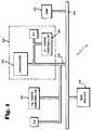
- the computer system Sincludes a microprocessor 20 that is connected to a first level cache C1 that is preferably located on the same chip 22 as the processor 20.
- the chip 22includes a C1 cache controller 30 that is connected to the C1 cache and controls the operation of the C1 cache.
- the processor 20, the first level cache C1, and the first level cache controller 30are connected to a system bus 24 through a local processor bus 25.
- a second level cache C2is connected to the local processor bus 25.
- a second level cache controller, referred to as the C2 cache controller 32,is connected to the C2 cache and the local processor bus 25.
- Random access memory 26, which is 4 Gigabytes in size according to the present embodiment, and an intelligent bus master 28are connected to the system bus 24.
- the random access memory (RAM) 26includes a system memory controller (not shown) that controls the operation of the RAM 26.
- the RAM 26 and the system memory controller (not shown)are hereinafter referred to as main memory 26.
- the system bus 24includes a data bus and a 32-bit address bus, the address bus including address bits A2 to A31, which allows access to any of 2 30 32-bit doublewords in main memory 26.
- the bus master 28may be any of the type that controls the system bus 24 when the processor system is on hold, such as the system direct memory access (DMA) controller, a hard disk interface, a local area network (LAN) interface or a video graphics processor system.
- DMAsystem direct memory access
- LANlocal area network
- the C1 and C2 cachesare aligned on a "way" basis such that a copy of data placed in a particular way in one of the caches can only be placed in a predetermined corresponding way in the other cache.
- This "way" alignmentrequires that the C2 cache have at least as many cache ways as does the C1 cache. If the C1 and C2 caches have the same number of ways, then there is a one-to-one correspondence between the cache ways in the C1 cache and the cache ways in the C2 cache. If the C2 cache has more cache ways than the C1 cache, then each cache way in the C1 cache corresponds to one or more cache ways in the C2 cache. However, no two C1 cache ways can correspond to the same C2 cache way.
- each memory addresshas only one possible location in each of the C1 and C2 caches. Accordingly, if two C1 cache ways corresponded to a single C2 cache way, then there would be memory address locations residing in the C1 cache that would be incapable of residing in the C2 cache. The respective C2 cache way location would be incapable of holding the two memory addresses which would reside in each of the respective C1 cache ways that corresponded to the respective C2 cache way location.
- each of the cachesis not important for the purposes of the invention.
- the C2 cachemust be at least as large as the C1 cache to achieve multilevel inclusion, and the C2 cache is preferably at least four times as large as the C1 cache to provide for an improved cache hit rate.
- the C1 cacheis 8 kbytes in size and the C2 cache is preferably 512 kbytes in size.
- the C1 cache and the C2 cacheare each 4-way set associative caches.
- the C1 and C2 cachesare each 2-way set-associative caches.
- FIG. 2 and 3conceptual diagrams of the C1 and C2 caches with their respective cache controllers 30 and 32 configured in a 2-way set-associative organization are generally shown.
- the following discussionis intended to provide an introduction to the structure and operation of a set-associative cache as well as the relationship between the cache memory, cache directories, and main memory 26.
- the C1 and C2 cachesare discussed with reference to a 2-way set-associative cache organization as a simpler example of the more complex 4-way set-associative cache organization of the preferred embodiment.
- the special cache controller design considerations that arise in a 4-way set-associative cache organization that do not occur in a 2-way set-associative organizationare noted in the following discussion.
- the C1 cacheincludes two banks or ways of memory, referred to as A1 and B1, which are each 4 kbytes in size. Each of the cache ways A1 and B1 are organized into 128 sets, with each set including eight lines 58 of memory storage. Each line includes one 32-bit doubleword, or four bytes of memory.
- Main memory 26is conceptually organized as 2 20 pages with a page size of 4 kbytes, which is equivalent to the size of each C1 cache way A1 and B1. Each conceptual page in main memory 26 includes 1024 lines, which is the same number of lines as have each of the cache ways A1 and B1. The unit of transfer between the main memory 26 and the C1 cache is one line.
- a particular line location, or page offset, from each of the pages in main memory 26,maps to the similarly located line in each of the cache ways A1 and B1.
- the page offset from each of the pages in main memory 26 that is shadedmaps to the equivalently located, and shaded, line offset in each of the cache ways A1 and B1.
- a particular page offset memory location from main memory 26can only map to one of two locations in the C1 cache, these locations being in each of the cache ways A1 and B1.
- Each of the cache ways A1 and B1include a cache directory, referred to as directory DA1 and directory DB1, respectively, that are located in the C1 cache controller 30 of the C1 cache.
- the directories DA1 and DB1each include one entry 60 and 62, respectively, for each of the 128 sets in the respective cache way A1 and B1.
- the cache directory entry for each sethas three components: a tag, a tag valid bit, and eight line valid bits, as shown.
- the number of line valid bitsequals the number of lines in each set.
- the 20 bits in the tag fieldhold the upper address bits, address bits A12 to A31, of the main memory address location of the copy of data that resides in the respective set of the cache.
- the upper address bitsaddress the appropriate 4 kbyte conceptual page in main memory 26 where the data in the respective set of the cache is located.
- the remaining address bits from this main memory address location, address bits A2 to A11can be partitioned into a set address field comprising seven bits, A5 to A11, which are used to select one of the 128 sets in the C1 cache, and a line address field comprising 3 bits, A2 to A4, which are used to select an individual line from the eight lines in the selected set. Therefore, the lower address bits A2 through A11 serve as the "cache address" which directly selects one of the line locations in each of the ways A1 and B1 of the C1 cache.
- the address bits A5 to A11are used to select one of the 128 sets, and the address bits A2 to A4 are used to select one of the respective line valid bits within each entry in the respective directories DA1 and DB1 from the selected set.
- the lower address bits A2 to A11are also used to select the appropriate line in the C1 cache.
- the cache controllercompares the upper address bit tag field of the requested memory address with each of the tags stored in the selected directory entries of the selected set for each of the cache ways A1 and B1. At the same time, both the tag valid and line valid bits are checked.
- the resultis a cache hit, and the corresponding cache way is directed to drive the selected line of data onto the data bus.
- a misscan occur in either of two ways. The first is known as a line miss and occurs when the upper address bits of the requested memory address match one of the tags in either of the directories DA1 or DB1 of the selected set and the respective tag valid bit is set, but the respective line valid bit(s) where the requested data resides are clear. The second is called a tag miss and occurs when either the upper address bits of the requested memory address do not match either of the respective tags in directories DA1 or DB1 of the selected set where the requested data is located, or the respective tag valid bit for each of the directories DA1 or DB1 are not clear.
- the C1 cache controller 30includes a replacement algorithm that determines which cache way, A1 or B1, in which to place new data.
- the replacement algorithm usedis a least recently used (LRU) algorithm that places new data in the cache way that was least recently accessed by the processor for data. This is because, statistically, the way most recently used is the way most likely to be needed again in the near future.
- the C1 cache controller 30includes a directory 70 that holds a LRU bit for each set in the cache, and the LRU bit is pointed away from the cache way that was most recently accessed by the processor. Therefore, if data requested by the processor resides in way A1, then the LRU bit is pointed toward B1. If the data requested by the processor resides in way B1, then the LRU bit is pointed toward A1.
- a more elaborate LRU or pseudo-LRU replacement algorithmcan be used in the C1 cache controller 30.
- the choice of a replacement algorithmis generally irrelevant to the present invention, and it is suggested that an LRU or pseudo-LRU algorithm be chosen to optimize the particular cache design used in the chosen embodiment.
- One replacement algorithm that can be used in the C1 cache controller 30 in the 4-way set-associative C1 cache organization of the preferred embodimentis a pseudo-LRU algorithm which operates as follows.
- the 4-way set-associative C1 cacheincludes four ways of memory referred to as W0, W1, W2, and W3.
- X0, X1, and X2are located in the C1 cache controller 30 and are defined for a respective set in each of the ways in the 4-way C1 cache. These bits are called LRU bits and are updated for every hit or replace in the C1 cache. If the most recent access in the respective set was to way W0 or way W1, then X0 is set to 1 or a logic high value. Bit X0 is set to 0 or a logic low value if the most recent access was to way W2 or way W3. If X0 is set to 1 and the most recent access between way W0 and way W1 was to way W0, then X1 is set to 1, otherwise X1 is set to 0. If X0 is set to 0 and the most recent access between way W2 and way W3 was to way W2, then X2 is set to 1, otherwise X2 is set to 0.
- the pseudo LRU replacement mechanismworks in the following manner.
- the C1 cache controller 30uses the X0 bit to first select the respective ways W0 and W1 or W2 and W3 where the particular line relocation candidate that was least recently used is located.
- the C1 cache controllerthen utilizes the X1 and X2 bits to determine which of the two selected cache ways W0 and W1 or W2 and W3 holds the respective line location that was least recently used, and this line location is marked for replacement.
- the C1 cache controller 30broadcasts its LRU information to the C2 cache controller 32 on C1 and C2 cache read misses and on processor writes according to the present invention.
- the C2 cache controller 32is able to place the copy of data that it receives from either the main memory 26 on read misses or from the processor 20 on processor writes into the C2 cache way corresponding to the C1 cache way where the C1 cache controller placed the copy of data, thereby achieving multilevel inclusion.
- the C1 cache controller 30ignores its LRU replacement algorithm on a C1 cache read miss and a C2 cache read hit so that the C1 cache controller 30 can place the copy of data that it receives from the C2 cache controller 32 in the C1 cache way corresponding to the C2 cache way where the read hit occurred.
- the 2-way set-associative C2 cacheis organized in a manner similar to that of the 2-way set-associative C1 cache.
- the C2 cachepreferably comprises 512 kbytes of cache data RAM.
- each cache way A2 and B2 in the C2 cacheis 256 kbytes in size and includes 8192 sets of eight lines each.
- the line size in the C2 cacheis one 32-bit doubleword, which is the same as that of the C1 cache.
- the 4 Gigabyte main memory 26is organized into 2 14 conceptual pages with each conceptual page being 256 kbytes in size.
- each line location or page offset in main memory 26maps to a similarly located line in each of the cache ways A2 and B2.
- the C2 cache controller 32includes cache way directories DA2 and DB2.
- the cache way directories DA2 and DB2have set entries which include 14-bit tag fields, as opposed to the 20-bit tag fields in the entries of the C1 cache directories DA1 and DB1.
- the 14-bit tag fieldshold the upper address bits, address bits A18 to A31, that address the appropriate 256 kbyte conceptual page in main memory 26 where the data in the respective set of the cache is located.
- the remaining address bits, A2 to A17can be partitioned into a set address field comprising thirteen bits, A5 to A17, which are used to select one of the 8192 mete in the C2 cache, and a line address field comprising 3 bits, A2 to A4, which are used to select an individual line from the eight lines in the selected set. Therefore, in the C2 cache the lower address bits A2 to A17 serve as the "cache address" which directly selects one of the line locations in each of the ways A2 and B2 of the C2 cache.
- the C2 cache controller 32does not generally require a replacement algorithm because the C2 cache receives new data only on C1 and C2 cache read misses and on processor writes, and in those instances the C2 cache controller receives the way location from the C1 cache controller and must fill the corresponding C2 cache way. Therefore, the C2 cache controller 32 does not need a replacement algorithm because the respective C2 cache way where data is placed is determined by the data's way location in the C1 cache. However, if the C2 cache has more ways than has the C1 cache, then the C2 cache controller 32 will require use of a replacement algorithm. In this instance, a C1 cache way will correspond to two or more C2 cache ways.
- the C2 cache controller 32will need a replacement algorithm in order to decide between the multiple C2 cache ways that correspond to the C1 cache way location in which to place the received data.
- the 2-way set-associative C1 and C2 cachesare aligned on a "way" basis such that the ways A1 and B1 in the C1 cache have a one-to-one correspondence with the ways A2 and B2, respectively, of the C2 cache.
- a page offset from main memory 26 that is placed in the respective line location in a C1 cache way A1 or B1has only one possible location in the corresponding C2 cache way A2 or B2, respectively.
- a respective line location in a C2 cache way A2 or B2has only one possible location in the corresponding C1 cache way A1 or B1, respectively.
- each of the C2 cache ways A2 or B2hold 64 lines of data that each correspond to, or could be located in, a single line or page offset location in the corresponding C1 cache way A1 or B1. Therefore, the C2 cache controller 32 according to the present invention includes inclusion bits 80 for each of its respective lines. This enables the C2 cache controller 32 to remember whether a copy of data from the respective C2 cache line also resides in the corresponding C1 cache line location.
- inclusion bits 80allows the C2 cache controller 32 to remember which of the 64 lines of data in the respective C2 cache way A2 or B2 that corresponds to a single C1 cache way location holds a copy of data that is duplicated in that C1 cache location. For example, if a line in the C2 cache receives a copy of data from main memory 26 that was also placed in the C1 cache, or if a line in the C2 cache provides a copy of data that is placed in the C1 cache, then an inclusion bit for the respective C2 cache line is true or set to a logic high value, signifying that the respective C2 cache line holds a copy of data that is duplicated in the respective C1 cache location.
- the other 63 line locations in the C2 cache which correspond to the respective C1 cache location involved in the above operationhave their inclusion bits cleared as a reminder that the copy of data that they hold is not duplicated in a C1 cache location. This is important because one of these other 63 line locations may hold data that was previously duplicated in the respective C1 cache location before one of the operations mentioned above placed new data in the respective C1 cache location, and therefore one of these 63 locations may have its inclusion bit set.
- the only instance where one of these other 63 C2 cache locations would not have its inclusion bit setis when the respective C2 cache line location that was involved in the above operation and had its inclusion bit set also held the copy of data that was duplicated in the respective C1 cache location before the operation took place and therefore already had its inclusion bit set.
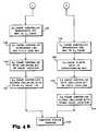
- Step 100represents that the computer system S is operating or turned on. In some computer systems, the processor is required to have control of the system bus 24 before it may issue memory reads or writes.
- the processor 20is not required to have control of the system bus 24 when it issues memory reads or writes but rather the processor 20 can operate out of the C1 cache and the C2 cache without requiring use of the system bus 24 until a C1 and C2 cache read miss or a processor write beyond any posting depth occurs.
- the C1 cache controller 30first checks the C1 cache in step 104 to determine if a copy of the requested main memory data resides in the C1 cache. If a copy of the requested data does not reside in the C1 cache, then a C1 cache read miss occurs in step 106, and the read operation is passed on to the C2 cache, where the C2 cache controller 32 then checks the C2 cache in step 108. If a copy of the requested data does not reside in the C2 cache, then a C2 cache read miss occurs in step 110, and the operation is passed onto the system memory controller to obtain the necessary data from main memory 26.
- Main memory 26provides the requested data to the C1 cache, the C2 cache and the processor 20 in step 112, and the C1 cache controller 30 places the data into one of its cache ways A1 or B1 according to its particular replacement algorithm in step 114.
- the datais placed in the C1 cache because of the statistical likelihood that this data will be requested again soon by the processor 20.
- the C1 cache controller 30 during this periodhas been broadcasting to the C2 cache controller 32 the particular C1 cache way A1 or B1 in which it is placing the data, represented in step 118, so that the C2 cache controller 32 can place the data in the corresponding C2 cache way A2 or B2 in step 120.
- the C2 cache controller 32sets the inclusion bit on the respective C2 cache memory location where the data is stored in step 122, signifying that a copy of the data in this location also resides in the C1 cache.
- the C2 cache controller 32also clears the inclusion bits on the other 63 C2 cache locations that correspond to the same page offset location in the C1 cache in step 124 to signify that a copy of the data in these locations does not reside in the C1 cache.
- the computer systemUpon completion of the memory read, the computer system returns to step 100.
- the C2 cache controller 32When the processor 20 initiates a main memory read in step 102 and the C2 cache controller 32 checks the C2 cache in step 108 after a C1 cache miss occurs in step 106, and a copy of the requested data resides in the C2 cache, then a C2 cache hit occurs in step 130.
- the C2 cache controller 32provides the requested data to the processor 20 in step 132, and also provides the data to the C1 cache in step 134 due to the statistical likelihood that this data will be requested again soon by the processor 20.
- the C2 cache controller 32informs the C1 cache controller 30 as to the particular C2 cache way A2 or B2 in which the data is located in the C2 cache in step 136 so that the C1 cache controller 30 can place the data in the corresponding C1 cache way A1 or B1 in step 138.
- the C1 and C2 cachesmaintain their "way" alignment without a requirement for the C2 cache controller 32 to transfer data between the ways in the C2 cache.
- the C2 cache controller 32sets the inclusion bit on the C2 cache location where the requested data is located in step 140, signifying that a copy of this data also resides in the C1 cache.
- the C2 cache controller 32also clears the other 63 inclusion bits on the C2 cache memory locations that correspond to the same page offset location to signify that a copy of the data in these locations does not reside in the C1 cache.
- the computer system Sis then finished with the memory read and returns to step 100.
- the processor 20initiates a memory read in step 102 and checks the contents of the C1 cache in step 104 to determine if a copy of the requested data resides there, and a copy of the requested data does reside in the C1 cache, then a C1 cache hit takes place in step 150.
- the C1 cache controller 30provides the requested data to the processor 20 in step 152, and operation of the computer system S is resumed in step 100. Since multilevel inclusion exists in the cache subsystem, the C2 cache is guaranteed to have a copy of the data that the C1 cache controller 30 provided to the processor 20, and no transfer of data from the C1 cache controller 30 to the C2 cache controller 32 is necessary when a C1 cache read hit takes place.
- the cache architecture of the C1 cache in the preferred embodimentis preferably a write-through cache architecture and the cache architecture of the C2 cache is preferably a write-back cache architecture.
- the use of other cache architectures for the C1 cache and the C2 cacheis also contemplated.
- the C1 and C2 cachesallocate write misses according to the present invention. It is preferred that the C1 and C2 either both allocate write misses or both do not allocate write misses. If the C1 cache were to not allocate writes and the C2 cache were to allocate writes, the designs would be more complicated.
- the C2 cache controller 32would require an LRU algorithm and would need to insure that if the C2 cache controller LRU algorithm selected a particular C2 cache way that contains a copy of data that is duplicated in the C1 cache, the LRU algorithm would be overridden or the caching aborted so that multilevel inclusion remained guaranteed.
- the C2 cache controller 32watches or "snoops" the system bus 24 in step 202 to see if the bus master 28 performs any writes, and reads in the case of a write-back cache, to main memory 26, and, if so, which memory location is being accessed.
- the C2 cache controller 32can perform the snooping responsibilities for both the C1 and C2 caches because the C2 cache is guaranteed to have a copy of all the data that resides in the C1 cache due to the multilevel inclusion.
- the C2 cache controller 32checks the inclusion bit for the respective C2 cache location to see whether the C1 cache controller 30 must also snoop the memory access in step 208. If the inclusion bit is not set in step 208, then a copy of the data from the memory location being written to does not reside in the C1 cache, and the C1 cache controller 30 is left alone. In this case, the C2 cache receives the new copy of data in step 210 and the C2 cache controller 32 resumes its snooping duties in step 202.
- the C2 cache controllerdirects the C1 cache controller 30 to snoop that particular memory access in step 212.
- the C1 and C2 cacheseach receive a copy of the new data, and the C2 cache controller 32 resumes its snooping duties in step 202.
- a snoop missoccurs in step 206 after the bus master 28 writes to a memory location in step 204, then the C2 cache controller 32 resumes its snooping duties in step 202.
- the C2 cache controller 32continues to snoop the system bus 24 in step 202 until the bus master 28 is no longer in control of the system bus 24.
- the C2 cache controller 32checks the C2 cache location in step 222 to determine if it is the owner of the respective memory location. If not, then main memory 26 or other source services the data request, and the C2 cache controller 32 resumes snooping in step 202. If the C2 cache controller 32 is the owner of the memory location, then the C2 cache controller 32 provides the requested data to main memory 26 in step 224. The bus master 28 reads this data in step 226 when the data has been placed on the data bus, this being referred to as snarfing.
- the C2 cache controller 32then resumes its snooping duties in step 202. If a snoop miss occurs in step 220 after the bus master 28 reads a memory location in step 204, then the C2 cache controller 32 resumes its snooping duties in step 202.
- the C1 cache controller 30can neglect its snooping duties until the C2 cache controller 32 determines that a snoop hit on data held in the C1 cache has actually occurred. This allows the processor 20 to operate more efficiently out of the C1 cache while it does not have control of the system bus 24 because the C1 cache controller 30 only has to snoop the system bus 24 when a C1 cache snoop hit occurs, not on every memory write as it normally would.
Landscapes
- Engineering & Computer Science (AREA)
- Theoretical Computer Science (AREA)
- Physics & Mathematics (AREA)
- General Engineering & Computer Science (AREA)
- General Physics & Mathematics (AREA)
- Memory System Of A Hierarchy Structure (AREA)
- Oscillators With Electromechanical Resonators (AREA)
Abstract
Description
Claims (12)
- A method for achieving multilevel inclusion ina computer system having a microprocessor (20), a systembus (24), a first level set associative cache (C1)including a first number of ways, a first level cachecontroller (30), a second level set associative cache (C2)including a second number of ways, a secondlevel cache controller (32), means coupled to the secondlevel cache controller for setting and clearing aninclusion bit on data inside the second level cache,means coupled to the first and second level cachecontrollers for communicating and transmitting databetween the first level and second level caches, a busmaster device (28), and a random access memory (26), the method beingcharacterized by:
having said second number of ways of the second level cache being equal to or greater than thefirst number of ways of the first level cache, whereineach of the ways in the first level cache correspondsto at least one way in the second level cache;the first level cache controller communicating tothe second level cache controller the particular firstlevel cache way in which a copy of data received fromthe random access memory is placed on a first level andsecond level cache read miss;the second level cache controller placing the copyof data received from the random access memory in thesecond level cache way corresponding to the first levelcache way communicated by the first level cachecontroller on the first level and second level cacheread miss;the second level cache controller communicating tothe first level cache controller the particular secondlevel cache way where a copy of data is located on afirst level cache read miss and second level cache readhit;the first level cache controller placing the copyof data transmitted from the second level cachecontroller to the processor in the corresponding firstlevel cache way; andthe second level cache controller setting aninclusion bit on the second level cache location of thecopy of data and clearing inclusion bits on any othersecond level cache locations that correspond to thefirst level cache location where the first level cachecontroller placed the copy of data. - The method of claim 1, wherein the first levelcache controller uses a replacement algorithm thatdetermines the first level cache way in which toplace a received copy of data, the step of the firstlevel cache controller copying the data into the firstlevel cache way corresponding to the second level cacheway including:
the first level cache controller disregarding itsreplacement algorithm on first level cache read missand second level cache read hit cases. - The method of claim 1, further comprising:the first level cache controller communicating tothe second level cache controller the particular firstlevel cache way in which a copy of received data isplaced on a processor write; andthe second level cache controller placing the copyof received data in the second level cache waycorresponding to the first level cache way communicatedby the first level cache controller;
- The method of claim 1, wherein more thanone way in the first level cache cannot correspond toone way in the second level cache and more than one way in the second level cache cancorrespond to one way in the first level cache.
- The method of claim 1, further comprising:the second level cache controller snooping thesystem bus when the processor does not have control ofthe system bus to determine if the bus master device iswriting to a cached memory location;the second level cache controller checking theinclusion bit on a second level cache location where asecond level cache write snoop hit occurs to determineif a copy of data from the random access memorylocation being written to resides in the first levelcache; andthe second level cache controller directing thefirst level cache controller to snoop the system bus ifsaid inclusion bit is set.
- The method of claim 5, wherein the secondlevel cache is a write-back cache, the method furthercomprising:the second level cache controller snooping thesystem bus when the processor does not have control ofthe system bus to determine if the bus master device isreading a cached memory location;the second level cache controller determining ifthe second level cache has an updated version of thedata residing in the requested memory location on asecond level cache read snoop hit;the second level cache controller providing therequested data to main memory if the second level cachehas an updated version of the data; andthe bus controller reading the requested dataprovided by the second level cache controller:
- An apparatus for achieving multilevelinclusion in a computer system, comprising:a system bus (24);a random access memory (26) coupled to said system bus;a microprocessor (20) coupled to said system bus;a first level set associative cache (C1) coupled to saidmicroprocessor and including a first number of ways;a first level cache controller (30) coupled to saidfirst level cache, said microprocessor and said systembus;a second level set associative cache (C2) of a size greater than orequal to the size of the first level cacheincluding a second number of ways andincluding inclusion information indicating presence ofdata in the second level cache that is duplicated inthe first level cache;a second level cache controller (31) coupled to saidsystem bus, said second level cache, saidmicroprocessor, and said first level cache controller;the apparatus being characterized by said second number of waysof the second level cache being equal to or greater than thefirst number of ways of the first level cache, whereineach of the ways in the first level cache correspondsto at least one way in the second level cache;said first level cache controller including an output for transmitting wayinformation and an input for receiving way information;said second level cache controllerincluding an input coupled to said first levelcache controller way information output for receivingway information and an output coupled to said firstlevel cache controller way information input fortransmitting way information; andwherein on a first and second level cache readmiss said first level cache controller is adapted to transmit wayinformation to said second level cache controller andsaid second level cache controller is adapted to place received datain a way of the second level cache corresponding to thereceived way information,wherein on a first level cache read miss and asecond level cache read hit said second level cachecontroller is adapted to transmit way information to said firstlevel cache controller and said first level cachecontroller is adapted to place received data in a way of the firstlevel cache corresponding to the received wayinformation, andwherein said second level cache controller is adapted to setthe inclusion bit in the second level cache locationwhich contains the data placed in the first level cacheand is adapted to clear the inclusion bits of any other second levelcache locations which correspond to the first levelcache location where the data was placed.
- The apparatus of claim 7, wherein said firstlevel cache controller includes a replacement meansthat determines the first level cache way in which toplace a received copy of data, wherein said first levelcache controller is adapted to disregard said replacement means onfirst level cache read miss and second level cache readhits cases.
- The apparatus of claim 7, wherein more thanone way in the first level cache cannot correspond toone way in the second level cache and morethan one way in the second level cache can correspondto one way in the first level cache.
- The apparatus of claim 7, wherein on aprocessor write said first level cache controller is adapted totransmit way information to said second level cachecontroller and said second level cache controller is adapted toplace received data in a way of the second level cachecorresponding to the received way information.
- The apparatus of claim 7, further comprising:a bus master device (28) coupled to said system bus;andwherein said first level cache controller includesmeans for snooping the system bus when saidmicroprocessor does not have control of said system busto determine if the bus master device is writing to arandom access memory location that is cached in thefirst level cache, andwherein said second level cache controller furtherincludes:means for snooping the system bus when saidmicroprocessor does not have control of said system busto determine if the bus master device is writing to arandom access memory location that is cached in thesecond level cache;means for checking the inclusion bit on a secondlevel cache location where a second level cache writesnoop hit occurs to determine if a copy of data fromsaid random access memory location being written toalso resides in said first level cache; andmeans coupled to said first level cache controllerfor directing said first level cache controller tosnoop the system bus if said inclusion bit is set.
- The apparatus of claim 11, furthercomprising:said second level cache being a write-back cache,wherein said second level cache controller furtherincludes:means for snooping the system bus when saidmicroprocessor does not have control of said system busto determine if the bus master device is reading arandom access memory location that is cached in thesecond level cache;means for determining whether the second levelcache includes an updated version of the data residingin the requested memory location when a second levelcache read snoop hit occurs; andmeans for providing the requested data to mainmemory if the second level cache has an updated versionof the data, wherein the bus controller reads therequested data provided by the second level cachecontroller.
Applications Claiming Priority (2)
| Application Number | Priority Date | Filing Date | Title |
|---|---|---|---|
| US53889490A | 1990-06-15 | 1990-06-15 | |
| US538894 | 1990-06-15 |
Publications (3)
| Publication Number | Publication Date |
|---|---|
| EP0461926A2 EP0461926A2 (en) | 1991-12-18 |
| EP0461926A3 EP0461926A3 (en) | 1992-05-06 |
| EP0461926B1true EP0461926B1 (en) | 1998-09-02 |
Family
ID=24148867
Family Applications (1)
| Application Number | Title | Priority Date | Filing Date |
|---|---|---|---|
| EP91305422AExpired - LifetimeEP0461926B1 (en) | 1990-06-15 | 1991-06-14 | Multilevel inclusion in multilevel cache hierarchies |
Country Status (6)
| Country | Link |
|---|---|
| US (1) | US5369753A (en) |
| EP (1) | EP0461926B1 (en) |
| JP (1) | JPH04233048A (en) |
| AT (1) | ATE170642T1 (en) |
| CA (1) | CA2044689A1 (en) |
| DE (1) | DE69130086T2 (en) |
Families Citing this family (129)
| Publication number | Priority date | Publication date | Assignee | Title |
|---|---|---|---|---|
| US5146473A (en) | 1989-08-14 | 1992-09-08 | International Mobile Machines Corporation | Subscriber unit for wireless digital subscriber communication system |
| EP0549219B1 (en)* | 1991-12-24 | 1998-06-10 | Motorola, Inc. | A cache controller |
| US5724549A (en)* | 1992-04-06 | 1998-03-03 | Cyrix Corporation | Cache coherency without bus master arbitration signals |
| US5524212A (en)* | 1992-04-27 | 1996-06-04 | University Of Washington | Multiprocessor system with write generate method for updating cache |
| JPH05324468A (en)* | 1992-05-21 | 1993-12-07 | Fujitsu Ltd | Hierarchical cache memory |
| JPH06110781A (en)* | 1992-09-30 | 1994-04-22 | Nec Corp | Cache memory device |
| EP0608622A1 (en)* | 1993-01-29 | 1994-08-03 | International Business Machines Corporation | Multiprocessor system with multilevel caches |
| EP0622738B1 (en)* | 1993-04-30 | 1998-08-05 | Siemens Nixdorf Informationssysteme Aktiengesellschaft | Method for carrying out requests to a multilevel cache memory in a data processing system and cache memory configurated accordingly |
| US5640531A (en)* | 1993-06-22 | 1997-06-17 | Unisys Corporation | Enhanced computer operational system using auxiliary mini-cache for enhancement to general cache |
| US5544342A (en)* | 1993-06-30 | 1996-08-06 | International Business Machines Corporation | System and method for prefetching information in a processing system |
| US5586270A (en)* | 1993-09-30 | 1996-12-17 | Intel Corporation | Method and apparatus for upgrading a central processing unit and existing memory structure in a computer system |
| US5636365A (en)* | 1993-10-05 | 1997-06-03 | Nec Corporation | Hierarchical buffer memories for selectively controlling data coherence including coherence control request means |
| US5530832A (en)* | 1993-10-14 | 1996-06-25 | International Business Machines Corporation | System and method for practicing essential inclusion in a multiprocessor and cache hierarchy |
| US5522057A (en)* | 1993-10-25 | 1996-05-28 | Intel Corporation | Hybrid write back/write through cache having a streamlined four state cache coherency protocol for uniprocessor computer systems |
| US5623627A (en)* | 1993-12-09 | 1997-04-22 | Advanced Micro Devices, Inc. | Computer memory architecture including a replacement cache |
| US5692154A (en)* | 1993-12-20 | 1997-11-25 | Compaq Computer Corporation | Circuit for masking a dirty status indication provided by a cache dirty memory under certain conditions so that a cache memory controller properly controls a cache tag memory |
| US5832534A (en)* | 1994-01-04 | 1998-11-03 | Intel Corporation | Method and apparatus for maintaining cache coherency using a single controller for multiple cache memories |
| US5603004A (en)* | 1994-02-14 | 1997-02-11 | Hewlett-Packard Company | Method for decreasing time penalty resulting from a cache miss in a multi-level cache system |
| US6006299A (en)* | 1994-03-01 | 1999-12-21 | Intel Corporation | Apparatus and method for caching lock conditions in a multi-processor system |
| US5717894A (en)* | 1994-03-07 | 1998-02-10 | Dell Usa, L.P. | Method and apparatus for reducing write cycle wait states in a non-zero wait state cache system |
| US5588131A (en)* | 1994-03-09 | 1996-12-24 | Sun Microsystems, Inc. | System and method for a snooping and snarfing cache in a multiprocessor computer system |
| JP2778913B2 (en)* | 1994-04-26 | 1998-07-23 | 株式会社東芝 | Multiprocessor system and memory allocation method |
| US5548742A (en)* | 1994-08-11 | 1996-08-20 | Intel Corporation | Method and apparatus for combining a direct-mapped cache and a multiple-way cache in a cache memory |
| US5813031A (en)* | 1994-09-21 | 1998-09-22 | Industrial Technology Research Institute | Caching tag for a large scale cache computer memory system |
| US5634073A (en)* | 1994-10-14 | 1997-05-27 | Compaq Computer Corporation | System having a plurality of posting queues associated with different types of write operations for selectively checking one queue based upon type of read operation |
| US6006312A (en)* | 1995-02-27 | 1999-12-21 | Sun Microsystems, Inc. | Cachability attributes of virtual addresses for optimizing performance of virtually and physically indexed caches in maintaining multiply aliased physical addresses |
| WO1996033462A1 (en)* | 1995-04-18 | 1996-10-24 | International Business Machines Corporation | Cache memory |
| US5623632A (en)* | 1995-05-17 | 1997-04-22 | International Business Machines Corporation | System and method for improving multilevel cache performance in a multiprocessing system |
| US5850534A (en)* | 1995-06-05 | 1998-12-15 | Advanced Micro Devices, Inc. | Method and apparatus for reducing cache snooping overhead in a multilevel cache system |
| US5740400A (en)* | 1995-06-05 | 1998-04-14 | Advanced Micro Devices Inc. | Reducing cache snooping overhead in a multilevel cache system with multiple bus masters and a shared level two cache by using an inclusion field |
| DE19524023B4 (en)* | 1995-06-30 | 2004-02-05 | Fujitsu Siemens Computers Gmbh | Multiprocessor system with a very large number of microprocessors |
| US5778427A (en)* | 1995-07-07 | 1998-07-07 | Sun Microsystems, Inc. | Method and apparatus for selecting a way of a multi-way associative cache by storing waylets in a translation structure |
| US5652859A (en)* | 1995-08-17 | 1997-07-29 | Institute For The Development Of Emerging Architectures, L.L.C. | Method and apparatus for handling snoops in multiprocessor caches having internal buffer queues |
| US5740399A (en)* | 1995-08-23 | 1998-04-14 | International Business Machines Corporation | Modified L1/L2 cache inclusion for aggressive prefetch |
| US5758119A (en)* | 1995-08-23 | 1998-05-26 | International Business Machines Corp. | System and method for indicating that a processor has prefetched data into a primary cache and not into a secondary cache |
| JP2964926B2 (en)* | 1995-08-29 | 1999-10-18 | 富士ゼロックス株式会社 | Database management apparatus and method |
| US5712970A (en)* | 1995-09-28 | 1998-01-27 | Emc Corporation | Method and apparatus for reliably storing data to be written to a peripheral device subsystem using plural controllers |
| US5809537A (en)* | 1995-12-08 | 1998-09-15 | International Business Machines Corp. | Method and system for simultaneous processing of snoop and cache operations |
| US5832250A (en)* | 1996-01-26 | 1998-11-03 | Unisys Corporation | Multi set cache structure having parity RAMs holding parity bits for tag data and for status data utilizing prediction circuitry that predicts and generates the needed parity bits |
| US6070233A (en)* | 1996-01-26 | 2000-05-30 | Unisys Corporation | Processor bus traffic optimization system for multi-level cache utilizing reflection status bit to indicate data inclusion in higher level cache |
| US5829038A (en)* | 1996-06-20 | 1998-10-27 | Intel Corporation | Backward inquiry to lower level caches prior to the eviction of a modified line from a higher level cache in a microprocessor hierarchical cache structure |
| US5835950A (en)* | 1996-07-12 | 1998-11-10 | Samsung Electronics Co., Ltd. | Self-invalidation method for reducing coherence overheads in a bus-based shared-memory multiprocessor apparatus |
| US6049847A (en)* | 1996-09-16 | 2000-04-11 | Corollary, Inc. | System and method for maintaining memory coherency in a computer system having multiple system buses |
| US5897656A (en) | 1996-09-16 | 1999-04-27 | Corollary, Inc. | System and method for maintaining memory coherency in a computer system having multiple system buses |
| US5926830A (en)* | 1996-10-07 | 1999-07-20 | International Business Machines Corporation | Data processing system and method for maintaining coherency between high and low level caches using inclusive states |
| US5809526A (en)* | 1996-10-28 | 1998-09-15 | International Business Machines Corporation | Data processing system and method for selective invalidation of outdated lines in a second level memory in response to a memory request initiated by a store operation |
| US6202125B1 (en) | 1996-11-25 | 2001-03-13 | Intel Corporation | Processor-cache protocol using simple commands to implement a range of cache configurations |
| US5809528A (en)* | 1996-12-24 | 1998-09-15 | International Business Machines Corporation | Method and circuit for a least recently used replacement mechanism and invalidated address handling in a fully associative many-way cache memory |
| US5787478A (en)* | 1997-03-05 | 1998-07-28 | International Business Machines Corporation | Method and system for implementing a cache coherency mechanism for utilization within a non-inclusive cache memory hierarchy |
| US5895495A (en)* | 1997-03-13 | 1999-04-20 | International Business Machines Corporation | Demand-based larx-reserve protocol for SMP system buses |
| US6374330B1 (en)* | 1997-04-14 | 2002-04-16 | International Business Machines Corporation | Cache-coherency protocol with upstream undefined state |
| US5943684A (en)* | 1997-04-14 | 1999-08-24 | International Business Machines Corporation | Method and system of providing a cache-coherency protocol for maintaining cache coherency within a multiprocessor data-processing system |
| US6105112A (en)* | 1997-04-14 | 2000-08-15 | International Business Machines Corporation | Dynamic folding of cache operations for multiple coherency-size systems |
| US6061755A (en)* | 1997-04-14 | 2000-05-09 | International Business Machines Corporation | Method of layering cache and architectural specific functions to promote operation symmetry |
| FR2762420B1 (en)* | 1997-04-16 | 1999-05-21 | Thomson Multimedia Sa | METHOD AND DEVICE FOR OBTAINING AN ADAPTIVE SELECTION OF DATA SETS STORED IN A MASS MEMORY |
| US5987577A (en)* | 1997-04-24 | 1999-11-16 | International Business Machines | Dual word enable method and apparatus for memory arrays |
| US6209072B1 (en) | 1997-05-06 | 2001-03-27 | Intel Corporation | Source synchronous interface between master and slave using a deskew latch |
| US5923898A (en)* | 1997-05-14 | 1999-07-13 | International Business Machines Corporation | System for executing I/O request when an I/O request queue entry matches a snoop table entry or executing snoop when not matched |
| US6065101A (en)* | 1997-06-12 | 2000-05-16 | International Business Machines Corporation | Pipelined snooping of multiple L1 cache lines |
| US5996048A (en)* | 1997-06-20 | 1999-11-30 | Sun Microsystems, Inc. | Inclusion vector architecture for a level two cache |
| US6115795A (en) | 1997-08-06 | 2000-09-05 | International Business Machines Corporation | Method and apparatus for configurable multiple level cache with coherency in a multiprocessor system |
| US6000015A (en)* | 1997-09-16 | 1999-12-07 | Unisys Corporation | Processor bus traffic optimization system for multi-level cache utilizing reflection status bit to indicate data inclusion in a higher level cache |
| US6073212A (en)* | 1997-09-30 | 2000-06-06 | Sun Microsystems, Inc. | Reducing bandwidth and areas needed for non-inclusive memory hierarchy by using dual tags |
| US5909697A (en)* | 1997-09-30 | 1999-06-01 | Sun Microsystems, Inc. | Reducing cache misses by snarfing writebacks in non-inclusive memory systems |
| US6321297B1 (en)* | 1998-01-05 | 2001-11-20 | Intel Corporation | Avoiding tag compares during writes in multi-level cache hierarchy |
| US6253291B1 (en)* | 1998-02-13 | 2001-06-26 | Sun Microsystems, Inc. | Method and apparatus for relaxing the FIFO ordering constraint for memory accesses in a multi-processor asynchronous cache system |
| US6094605A (en)* | 1998-07-06 | 2000-07-25 | Storage Technology Corporation | Virtual automated cartridge system |
| US6405322B1 (en) | 1999-04-13 | 2002-06-11 | Hewlett-Packard Company | System and method for recovery from address errors |
| US6510493B1 (en) | 1999-07-15 | 2003-01-21 | International Business Machines Corporation | Method and apparatus for managing cache line replacement within a computer system |
| US6324617B1 (en) | 1999-08-04 | 2001-11-27 | International Business Machines Corporation | Method and system for communicating tags of data access target and castout victim in a single data transfer |
| US6343347B1 (en) | 1999-08-04 | 2002-01-29 | International Business Machines Corporation | Multiprocessor system bus with cache state and LRU snoop responses for read/castout (RCO) address transaction |
| US6343344B1 (en) | 1999-08-04 | 2002-01-29 | International Business Machines Corporation | System bus directory snooping mechanism for read/castout (RCO) address transaction |
| US6338124B1 (en) | 1999-08-04 | 2002-01-08 | International Business Machines Corporation | Multiprocessor system bus with system controller explicitly updating snooper LRU information |
| US6502171B1 (en)* | 1999-08-04 | 2002-12-31 | International Business Machines Corporation | Multiprocessor system bus with combined snoop responses explicitly informing snoopers to scarf data |
| US6353875B1 (en) | 1999-08-04 | 2002-03-05 | International Business Machines Corporation | Upgrading of snooper cache state mechanism for system bus with read/castout (RCO) address transactions |
| US6349367B1 (en) | 1999-08-04 | 2002-02-19 | International Business Machines Corporation | Method and system for communication in which a castout operation is cancelled in response to snoop responses |
| US6321305B1 (en) | 1999-08-04 | 2001-11-20 | International Business Machines Corporation | Multiprocessor system bus with combined snoop responses explicitly cancelling master allocation of read data |
| US6587923B1 (en)* | 2000-05-22 | 2003-07-01 | International Business Machines Corporation | Dual line size cache directory |
| US6725341B1 (en)* | 2000-06-28 | 2004-04-20 | Intel Corporation | Cache line pre-load and pre-own based on cache coherence speculation |
| US6732234B1 (en)* | 2000-08-07 | 2004-05-04 | Broadcom Corporation | Direct access mode for a cache |
| US6748492B1 (en)* | 2000-08-07 | 2004-06-08 | Broadcom Corporation | Deterministic setting of replacement policy in a cache through way selection |
| US6848024B1 (en)* | 2000-08-07 | 2005-01-25 | Broadcom Corporation | Programmably disabling one or more cache entries |
| US6721856B1 (en)* | 2000-10-26 | 2004-04-13 | International Business Machines Corporation | Enhanced cache management mechanism via an intelligent system bus monitor |
| US6631450B1 (en)* | 2000-10-26 | 2003-10-07 | International Business Machines Corporation | Symmetric multiprocessor address bus protocol with intra-cache line access information |
| US6704843B1 (en) | 2000-10-26 | 2004-03-09 | International Business Machines Corporation | Enhanced multiprocessor response bus protocol enabling intra-cache line reference exchange |
| US6601144B1 (en) | 2000-10-26 | 2003-07-29 | International Business Machines Corporation | Dynamic cache management in a symmetric multiprocessor system via snoop operation sequence analysis |
| US6629210B1 (en) | 2000-10-26 | 2003-09-30 | International Business Machines Corporation | Intelligent cache management mechanism via processor access sequence analysis |
| US6763433B1 (en) | 2000-10-26 | 2004-07-13 | International Business Machines Corporation | High performance cache intervention mechanism for symmetric multiprocessor systems |
| US6826662B2 (en) | 2001-03-22 | 2004-11-30 | Sony Computer Entertainment Inc. | System and method for data synchronization for a computer architecture for broadband networks |
| US7231500B2 (en) | 2001-03-22 | 2007-06-12 | Sony Computer Entertainment Inc. | External data interface in a computer architecture for broadband networks |
| US6526491B2 (en) | 2001-03-22 | 2003-02-25 | Sony Corporation Entertainment Inc. | Memory protection system and method for computer architecture for broadband networks |
| US7093104B2 (en) | 2001-03-22 | 2006-08-15 | Sony Computer Entertainment Inc. | Processing modules for computer architecture for broadband networks |
| US7233998B2 (en) | 2001-03-22 | 2007-06-19 | Sony Computer Entertainment Inc. | Computer architecture and software cells for broadband networks |
| US7516334B2 (en) | 2001-03-22 | 2009-04-07 | Sony Computer Entertainment Inc. | Power management for processing modules |
| US6809734B2 (en) | 2001-03-22 | 2004-10-26 | Sony Computer Entertainment Inc. | Resource dedication system and method for a computer architecture for broadband networks |
| US6748495B2 (en) | 2001-05-15 | 2004-06-08 | Broadcom Corporation | Random generator |
| US6662272B2 (en)* | 2001-09-29 | 2003-12-09 | Hewlett-Packard Development Company, L.P. | Dynamic cache partitioning |
| US7114038B2 (en)* | 2001-12-28 | 2006-09-26 | Intel Corporation | Method and apparatus for communicating between integrated circuits in a low power mode |
| US6983348B2 (en)* | 2002-01-24 | 2006-01-03 | Intel Corporation | Methods and apparatus for cache intervention |
| US7100001B2 (en)* | 2002-01-24 | 2006-08-29 | Intel Corporation | Methods and apparatus for cache intervention |
| US7024519B2 (en)* | 2002-05-06 | 2006-04-04 | Sony Computer Entertainment Inc. | Methods and apparatus for controlling hierarchical cache memory |
| US7266587B2 (en)* | 2002-05-15 | 2007-09-04 | Broadcom Corporation | System having interfaces, switch, and memory bridge for CC-NUMA operation |
| US20040153611A1 (en)* | 2003-02-04 | 2004-08-05 | Sujat Jamil | Methods and apparatus for detecting an address conflict |
| US7287126B2 (en)* | 2003-07-30 | 2007-10-23 | Intel Corporation | Methods and apparatus for maintaining cache coherency |
| US7093075B2 (en)* | 2003-11-07 | 2006-08-15 | International Business Machines Corporation | Location-based placement algorithms for set associative cache memory |
| US7236918B2 (en)* | 2003-12-31 | 2007-06-26 | International Business Machines Corporation | Method and system for selective compilation of instrumentation entities into a simulation model of a digital design |
| US7213107B2 (en)* | 2003-12-31 | 2007-05-01 | Intel Corporation | Dedicated cache memory |
| US8224639B2 (en) | 2004-03-29 | 2012-07-17 | Sony Computer Entertainment Inc. | Methods and apparatus for achieving thermal management using processing task scheduling |
| JP4673584B2 (en)* | 2004-07-29 | 2011-04-20 | 富士通株式会社 | Cache memory device, arithmetic processing device, and control method for cache memory device |
| US20060089826A1 (en)* | 2004-10-21 | 2006-04-27 | International Business Machines Corporation | Method, system and program product for defining and recording minimum and maximum count events of a simulation |
| US7392169B2 (en)* | 2004-10-21 | 2008-06-24 | International Business Machines Corporation | Method, system and program product for defining and recording minimum and maximum event counts of a simulation utilizing a high level language |
| US7454325B2 (en)* | 2004-12-07 | 2008-11-18 | International Business Machines Corporation | Method, system and program product for defining and recording threshold-qualified count events of a simulation by testcases |
| US7552043B2 (en)* | 2005-09-15 | 2009-06-23 | International Business Machines Corporation | Method, system and program product for selectively removing instrumentation logic from a simulation model |
| US7711537B2 (en)* | 2006-05-03 | 2010-05-04 | International Business Machines Corporation | Signals for simulation result viewing |
| US7493248B2 (en)* | 2006-05-08 | 2009-02-17 | International Business Machines Corporation | Method, system and program product supporting phase events in a simulation model of a digital system |
| US7912694B2 (en)* | 2007-01-30 | 2011-03-22 | International Business Machines Corporation | Print events in the simulation of a digital system |
| US7917699B2 (en) | 2007-12-21 | 2011-03-29 | Mips Technologies, Inc. | Apparatus and method for controlling the exclusivity mode of a level-two cache |
| US7890699B2 (en)* | 2008-01-10 | 2011-02-15 | International Business Machines Corporation | Processing unit incorporating L1 cache bypass |
| KR20100058825A (en)* | 2008-11-25 | 2010-06-04 | 삼성전자주식회사 | Semiconductor device using variable resistive element, card or system using the same and operating method the semiconductor device |
| US8782374B2 (en)* | 2008-12-02 | 2014-07-15 | Intel Corporation | Method and apparatus for inclusion of TLB entries in a micro-op cache of a processor |
| US8453080B2 (en)* | 2008-12-16 | 2013-05-28 | International Business Machines Corporation | Model build in the presence of a non-binding reference |
| JP5440067B2 (en)* | 2009-09-18 | 2014-03-12 | 富士通株式会社 | Cache memory control device and cache memory control method |
| US8504774B2 (en) | 2010-10-13 | 2013-08-06 | Microsoft Corporation | Dynamic cache configuration using separate read and write caches |
| US10102129B2 (en)* | 2015-12-21 | 2018-10-16 | Intel Corporation | Minimizing snoop traffic locally and across cores on a chip multi-core fabric |
| US10635766B2 (en) | 2016-12-12 | 2020-04-28 | International Business Machines Corporation | Simulation employing level-dependent multitype events |
| US10366008B2 (en)* | 2016-12-12 | 2019-07-30 | Advanced Micro Devices, Inc. | Tag and data organization in large memory caches |
| US10417135B2 (en)* | 2017-09-28 | 2019-09-17 | Intel Corporation | Near memory miss prediction to reduce memory access latency |
| TWI697902B (en) | 2019-01-24 | 2020-07-01 | 瑞昱半導體股份有限公司 | Electronic device and method for managing electronic device |
| CN112433961B (en)* | 2020-12-02 | 2022-07-08 | 海光信息技术股份有限公司 | Compound cache directory system and management method thereof |
Family Cites Families (17)
| Publication number | Priority date | Publication date | Assignee | Title |
|---|---|---|---|---|
| US4464712A (en)* | 1981-07-06 | 1984-08-07 | International Business Machines Corporation | Second level cache replacement method and apparatus |
| US4442487A (en)* | 1981-12-31 | 1984-04-10 | International Business Machines Corporation | Three level memory hierarchy using write and share flags |
| US4493026A (en)* | 1982-05-26 | 1985-01-08 | International Business Machines Corporation | Set associative sector cache |
| US4736293A (en)* | 1984-04-11 | 1988-04-05 | American Telephone And Telegraph Company, At&T Bell Laboratories | Interleaved set-associative memory |
| US4823259A (en)* | 1984-06-29 | 1989-04-18 | International Business Machines Corporation | High speed buffer store arrangement for quick wide transfer of data |
| US4985829A (en)* | 1984-07-31 | 1991-01-15 | Texas Instruments Incorporated | Cache hierarchy design for use in a memory management unit |
| US4774654A (en)* | 1984-12-24 | 1988-09-27 | International Business Machines Corporation | Apparatus and method for prefetching subblocks from a low speed memory to a high speed memory of a memory hierarchy depending upon state of replacing bit in the low speed memory |
| US4755930A (en)* | 1985-06-27 | 1988-07-05 | Encore Computer Corporation | Hierarchical cache memory system and method |
| US4783736A (en)* | 1985-07-22 | 1988-11-08 | Alliant Computer Systems Corporation | Digital computer with multisection cache |
| US5091846A (en)* | 1986-10-03 | 1992-02-25 | Intergraph Corporation | Cache providing caching/non-caching write-through and copyback modes for virtual addresses and including bus snooping to maintain coherency |
| US5023776A (en)* | 1988-02-22 | 1991-06-11 | International Business Machines Corp. | Store queue for a tightly coupled multiple processor configuration with two-level cache buffer storage |
| US5202972A (en)* | 1988-12-29 | 1993-04-13 | International Business Machines Corporation | Store buffer apparatus in a multiprocessor system |
| US5133074A (en)* | 1989-02-08 | 1992-07-21 | Acer Incorporated | Deadlock resolution with cache snooping |
| US5072369A (en)* | 1989-04-07 | 1991-12-10 | Tektronix, Inc. | Interface between buses attached with cached modules providing address space mapped cache coherent memory access with SNOOP hit memory updates |
| US5136700A (en)* | 1989-12-22 | 1992-08-04 | Digital Equipment Corporation | Apparatus and method for reducing interference in two-level cache memories |
| US5253353A (en)* | 1990-01-02 | 1993-10-12 | Digital Equipment Corporation | System and method for efficiently supporting access to I/O devices through large direct-mapped data caches |
| US5163140A (en)* | 1990-02-26 | 1992-11-10 | Nexgen Microsystems | Two-level branch prediction cache |
- 1991
- 1991-06-14EPEP91305422Apatent/EP0461926B1/ennot_activeExpired - Lifetime
- 1991-06-14ATAT91305422Tpatent/ATE170642T1/ennot_activeIP Right Cessation
- 1991-06-14CACA002044689Apatent/CA2044689A1/ennot_activeAbandoned
- 1991-06-14DEDE69130086Tpatent/DE69130086T2/ennot_activeExpired - Fee Related
- 1991-06-15JPJP3170565Apatent/JPH04233048A/enactivePending
- 1993
- 1993-05-27USUS08/068,294patent/US5369753A/ennot_activeExpired - Lifetime
Also Published As
| Publication number | Publication date |
|---|---|
| DE69130086D1 (en) | 1998-10-08 |
| JPH04233048A (en) | 1992-08-21 |
| US5369753A (en) | 1994-11-29 |
| DE69130086T2 (en) | 1999-01-21 |
| EP0461926A2 (en) | 1991-12-18 |
| EP0461926A3 (en) | 1992-05-06 |
| ATE170642T1 (en) | 1998-09-15 |
| CA2044689A1 (en) | 1991-12-16 |
Similar Documents
| Publication | Publication Date | Title |
|---|---|---|
| EP0461926B1 (en) | Multilevel inclusion in multilevel cache hierarchies | |
| US5325504A (en) | Method and apparatus for incorporating cache line replacement and cache write policy information into tag directories in a cache system | |
| US7698508B2 (en) | System and method for reducing unnecessary cache operations | |
| US5802572A (en) | Write-back cache having sub-line size coherency granularity and method for maintaining coherency within a write-back cache | |
| US7237068B2 (en) | Computer system employing bundled prefetching and null-data packet transmission | |
| US7032074B2 (en) | Method and mechanism to use a cache to translate from a virtual bus to a physical bus | |
| US6345342B1 (en) | Cache coherency protocol employing a read operation including a programmable flag to indicate deallocation of an intervened cache line | |
| US6571322B2 (en) | Multiprocessor computer system with sectored cache line mechanism for cache intervention | |
| US7827354B2 (en) | Victim cache using direct intervention | |
| JP3281893B2 (en) | Method and system for implementing a cache coherency mechanism utilized within a cache memory hierarchy | |
| EP0800137B1 (en) | Memory controller | |
| US6343347B1 (en) | Multiprocessor system bus with cache state and LRU snoop responses for read/castout (RCO) address transaction | |
| US6185658B1 (en) | Cache with enhanced victim selection using the coherency states of cache lines | |
| US7305523B2 (en) | Cache memory direct intervention | |
| US6321306B1 (en) | High performance multiprocessor system with modified-unsolicited cache state | |
| US20020078304A1 (en) | System and method for allocating a directory entry for use in multiprocessor-node data processing systems | |
| US7281092B2 (en) | System and method of managing cache hierarchies with adaptive mechanisms | |
| US7117312B1 (en) | Mechanism and method employing a plurality of hash functions for cache snoop filtering | |
| US7325102B1 (en) | Mechanism and method for cache snoop filtering | |
| US8473686B2 (en) | Computer cache system with stratified replacement | |
| US5809537A (en) | Method and system for simultaneous processing of snoop and cache operations | |
| US7380068B2 (en) | System and method for contention-based cache performance optimization | |
| US6345344B1 (en) | Cache allocation mechanism for modified-unsolicited cache state that modifies victimization priority bits | |
| US6349367B1 (en) | Method and system for communication in which a castout operation is cancelled in response to snoop responses | |
| US6279086B1 (en) | Multiprocessor system bus with combined snoop responses implicitly updating snooper LRU position |
Legal Events
| Date | Code | Title | Description |
|---|---|---|---|
| PUAI | Public reference made under article 153(3) epc to a published international application that has entered the european phase | Free format text:ORIGINAL CODE: 0009012 | |
| AK | Designated contracting states | Kind code of ref document:A2 Designated state(s):AT BE CH DE DK ES FR GB GR IT LI LU NL SE | |
| PUAL | Search report despatched | Free format text:ORIGINAL CODE: 0009013 | |
| AK | Designated contracting states | Kind code of ref document:A3 Designated state(s):AT BE CH DE DK ES FR GB GR IT LI LU NL SE | |
| 17P | Request for examination filed | Effective date:19921023 | |
| GRAG | Despatch of communication of intention to grant | Free format text:ORIGINAL CODE: EPIDOS AGRA | |
| 17Q | First examination report despatched | Effective date:19971028 | |
| GRAG | Despatch of communication of intention to grant | Free format text:ORIGINAL CODE: EPIDOS AGRA | |
| GRAH | Despatch of communication of intention to grant a patent | Free format text:ORIGINAL CODE: EPIDOS IGRA | |
| GRAH | Despatch of communication of intention to grant a patent | Free format text:ORIGINAL CODE: EPIDOS IGRA | |
| GRAA | (expected) grant | Free format text:ORIGINAL CODE: 0009210 | |
| AK | Designated contracting states | Kind code of ref document:B1 Designated state(s):AT BE CH DE DK ES FR GB GR IT LI LU NL SE | |
| PG25 | Lapsed in a contracting state [announced via postgrant information from national office to epo] | Ref country code:IT Free format text:LAPSE BECAUSE OF FAILURE TO SUBMIT A TRANSLATION OF THE DESCRIPTION OR TO PAY THE FEE WITHIN THE PRE;WARNING: LAPSES OF ITALIAN PATENTS WITH EFFECTIVE DATE BEFORE 2007 MAY HAVE OCCURRED AT ANY TIME BEFORE 2007. THE CORRECT EFFECTIVE DATE MAY BE DIFFERENT FROM THE ONE RECORDED.SCRIBED TIME-LIMIT Effective date:19980902 Ref country code:NL Free format text:LAPSE BECAUSE OF FAILURE TO SUBMIT A TRANSLATION OF THE DESCRIPTION OR TO PAY THE FEE WITHIN THE PRESCRIBED TIME-LIMIT Effective date:19980902 Ref country code:AT Free format text:LAPSE BECAUSE OF FAILURE TO SUBMIT A TRANSLATION OF THE DESCRIPTION OR TO PAY THE FEE WITHIN THE PRESCRIBED TIME-LIMIT Effective date:19980902 Ref country code:LI Free format text:LAPSE BECAUSE OF FAILURE TO SUBMIT A TRANSLATION OF THE DESCRIPTION OR TO PAY THE FEE WITHIN THE PRESCRIBED TIME-LIMIT Effective date:19980902 Ref country code:GR Free format text:LAPSE BECAUSE OF NON-PAYMENT OF DUE FEES Effective date:19980902 Ref country code:CH Free format text:LAPSE BECAUSE OF FAILURE TO SUBMIT A TRANSLATION OF THE DESCRIPTION OR TO PAY THE FEE WITHIN THE PRESCRIBED TIME-LIMIT Effective date:19980902 Ref country code:BE Free format text:LAPSE BECAUSE OF FAILURE TO SUBMIT A TRANSLATION OF THE DESCRIPTION OR TO PAY THE FEE WITHIN THE PRESCRIBED TIME-LIMIT Effective date:19980902 Ref country code:ES Free format text:THE PATENT HAS BEEN ANNULLED BY A DECISION OF A NATIONAL AUTHORITY Effective date:19980902 | |
| REF | Corresponds to: | Ref document number:170642 Country of ref document:AT Date of ref document:19980915 Kind code of ref document:T | |
| REG | Reference to a national code | Ref country code:CH Ref legal event code:EP | |
| REF | Corresponds to: | Ref document number:69130086 Country of ref document:DE Date of ref document:19981008 | |
| PG25 | Lapsed in a contracting state [announced via postgrant information from national office to epo] | Ref country code:SE Free format text:LAPSE BECAUSE OF FAILURE TO SUBMIT A TRANSLATION OF THE DESCRIPTION OR TO PAY THE FEE WITHIN THE PRESCRIBED TIME-LIMIT Effective date:19981202 Ref country code:DK Free format text:LAPSE BECAUSE OF FAILURE TO SUBMIT A TRANSLATION OF THE DESCRIPTION OR TO PAY THE FEE WITHIN THE PRESCRIBED TIME-LIMIT Effective date:19981202 | |
| ET | Fr: translation filed | ||
| NLV1 | Nl: lapsed or annulled due to failure to fulfill the requirements of art. 29p and 29m of the patents act | ||
| REG | Reference to a national code | Ref country code:CH Ref legal event code:PL | |
| PG25 | Lapsed in a contracting state [announced via postgrant information from national office to epo] | Ref country code:LU Free format text:LAPSE BECAUSE OF NON-PAYMENT OF DUE FEES Effective date:19990614 | |
| PLBE | No opposition filed within time limit | Free format text:ORIGINAL CODE: 0009261 | |
| STAA | Information on the status of an ep patent application or granted ep patent | Free format text:STATUS: NO OPPOSITION FILED WITHIN TIME LIMIT | |
| 26N | No opposition filed | ||
| REG | Reference to a national code | Ref country code:GB Ref legal event code:IF02 | |
| PGFP | Annual fee paid to national office [announced via postgrant information from national office to epo] | Ref country code:DE Payment date:20070731 Year of fee payment:17 | |
| PGFP | Annual fee paid to national office [announced via postgrant information from national office to epo] | Ref country code:GB Payment date:20070628 Year of fee payment:17 | |
| PGFP | Annual fee paid to national office [announced via postgrant information from national office to epo] | Ref country code:FR Payment date:20070618 Year of fee payment:17 | |
| GBPC | Gb: european patent ceased through non-payment of renewal fee | Effective date:20080614 | |
| REG | Reference to a national code | Ref country code:FR Ref legal event code:ST Effective date:20090228 | |
| PG25 | Lapsed in a contracting state [announced via postgrant information from national office to epo] | Ref country code:DE Free format text:LAPSE BECAUSE OF NON-PAYMENT OF DUE FEES Effective date:20090101 | |
| PG25 | Lapsed in a contracting state [announced via postgrant information from national office to epo] | Ref country code:GB Free format text:LAPSE BECAUSE OF NON-PAYMENT OF DUE FEES Effective date:20080614 | |
| PG25 | Lapsed in a contracting state [announced via postgrant information from national office to epo] | Ref country code:FR Free format text:LAPSE BECAUSE OF NON-PAYMENT OF DUE FEES Effective date:20080630 |