EP0455070B1 - Capacitive sensor with frequency output - Google Patents
Capacitive sensor with frequency outputDownload PDFInfo
- Publication number
- EP0455070B1 EP0455070B1EP91106333AEP91106333AEP0455070B1EP 0455070 B1EP0455070 B1EP 0455070B1EP 91106333 AEP91106333 AEP 91106333AEP 91106333 AEP91106333 AEP 91106333AEP 0455070 B1EP0455070 B1EP 0455070B1
- Authority
- EP
- European Patent Office
- Prior art keywords
- base body
- capacitive sensor
- silicon
- electrodes
- ring oscillator
- Prior art date
- Legal status (The legal status is an assumption and is not a legal conclusion. Google has not performed a legal analysis and makes no representation as to the accuracy of the status listed.)
- Expired - Lifetime
Links
Images

Classifications
- G—PHYSICS
- G01—MEASURING; TESTING
- G01L—MEASURING FORCE, STRESS, TORQUE, WORK, MECHANICAL POWER, MECHANICAL EFFICIENCY, OR FLUID PRESSURE
- G01L9/00—Measuring steady of quasi-steady pressure of fluid or fluent solid material by electric or magnetic pressure-sensitive elements; Transmitting or indicating the displacement of mechanical pressure-sensitive elements, used to measure the steady or quasi-steady pressure of a fluid or fluent solid material, by electric or magnetic means
- G01L9/0041—Transmitting or indicating the displacement of flexible diaphragms
- G01L9/0072—Transmitting or indicating the displacement of flexible diaphragms using variations in capacitance
- G01L9/0073—Transmitting or indicating the displacement of flexible diaphragms using variations in capacitance using a semiconductive diaphragm
- G—PHYSICS
- G01—MEASURING; TESTING
- G01D—MEASURING NOT SPECIALLY ADAPTED FOR A SPECIFIC VARIABLE; ARRANGEMENTS FOR MEASURING TWO OR MORE VARIABLES NOT COVERED IN A SINGLE OTHER SUBCLASS; TARIFF METERING APPARATUS; MEASURING OR TESTING NOT OTHERWISE PROVIDED FOR
- G01D5/00—Mechanical means for transferring the output of a sensing member; Means for converting the output of a sensing member to another variable where the form or nature of the sensing member does not constrain the means for converting; Transducers not specially adapted for a specific variable
- G01D5/12—Mechanical means for transferring the output of a sensing member; Means for converting the output of a sensing member to another variable where the form or nature of the sensing member does not constrain the means for converting; Transducers not specially adapted for a specific variable using electric or magnetic means
- G01D5/14—Mechanical means for transferring the output of a sensing member; Means for converting the output of a sensing member to another variable where the form or nature of the sensing member does not constrain the means for converting; Transducers not specially adapted for a specific variable using electric or magnetic means influencing the magnitude of a current or voltage
- G01D5/24—Mechanical means for transferring the output of a sensing member; Means for converting the output of a sensing member to another variable where the form or nature of the sensing member does not constrain the means for converting; Transducers not specially adapted for a specific variable using electric or magnetic means influencing the magnitude of a current or voltage by varying capacitance
- G01D5/241—Mechanical means for transferring the output of a sensing member; Means for converting the output of a sensing member to another variable where the form or nature of the sensing member does not constrain the means for converting; Transducers not specially adapted for a specific variable using electric or magnetic means influencing the magnitude of a current or voltage by varying capacitance by relative movement of capacitor electrodes
- G01D5/2417—Mechanical means for transferring the output of a sensing member; Means for converting the output of a sensing member to another variable where the form or nature of the sensing member does not constrain the means for converting; Transducers not specially adapted for a specific variable using electric or magnetic means influencing the magnitude of a current or voltage by varying capacitance by relative movement of capacitor electrodes by varying separation
- G—PHYSICS
- G01—MEASURING; TESTING
- G01L—MEASURING FORCE, STRESS, TORQUE, WORK, MECHANICAL POWER, MECHANICAL EFFICIENCY, OR FLUID PRESSURE
- G01L9/00—Measuring steady of quasi-steady pressure of fluid or fluent solid material by electric or magnetic pressure-sensitive elements; Transmitting or indicating the displacement of mechanical pressure-sensitive elements, used to measure the steady or quasi-steady pressure of a fluid or fluent solid material, by electric or magnetic means
- G01L9/12—Measuring steady of quasi-steady pressure of fluid or fluent solid material by electric or magnetic pressure-sensitive elements; Transmitting or indicating the displacement of mechanical pressure-sensitive elements, used to measure the steady or quasi-steady pressure of a fluid or fluent solid material, by electric or magnetic means by making use of variations in capacitance, i.e. electric circuits therefor
- G01L9/125—Measuring steady of quasi-steady pressure of fluid or fluent solid material by electric or magnetic pressure-sensitive elements; Transmitting or indicating the displacement of mechanical pressure-sensitive elements, used to measure the steady or quasi-steady pressure of a fluid or fluent solid material, by electric or magnetic means by making use of variations in capacitance, i.e. electric circuits therefor with temperature compensating means
Definitions
- the inventionrelates to a capacitive sensor according to the preamble of claim 1.
- the capacitance of a measuring capacitoris changed by the action of a measured variable.
- This change in capacitanceserves as a measure of the measured variable to be recorded.
- the change in capacitancecan have different causes depending on the properties of this measured variable.
- Capacitive sensorsare particularly suitable for measuring mechanical quantities, for example force, pressure or acceleration, in which, under the effect of the quantity to be measured, a body provided with electrodes is mechanically deflected relative to another electrode and the associated change in capacitance is detected.
- capacitive sensors for measuring mechanical quantitieshave the advantage of a lower temperature dependence and a higher sensitivity.
- sensorsare particularly advantageous which convert a measurement variable to be detected into a frequency-analog electrical output signal.
- Frequency signalscan largely be transmitted without interference are and are suitable for digital processing without subsequent analog-digital conversion.
- the measuring capacitance of the sensoris interconnected in a ring oscillator circuit together with a further, predetermined capacitance and several resistors and inverters.
- the oscillation frequency of this ring oscillatorchanges with the measuring capacity and is therefore a measure of the quantity of coolant flowing in a coolant line as a measured variable (US Pat. No. 4,344,293).
- a capacitive sensorIn a further known embodiment of a capacitive sensor, several identical measuring capacitors are connected as frequency-determining elements together with an identical number of inverters in a ring oscillator. Each measuring capacitance is dependent on the same measured variable and is assigned to exactly one inverter of the ring oscillator. Several such ring oscillators can also be provided. A digital output signal for the measured variable to be determined is derived from the frequency-analog signals of the ring oscillators with the aid of a digital counter.
- the measuring capacitors and the other components of the ring oscillatorare implemented separately as discrete components (Patent Abstracts of Japan, Vol. 10, No. 106, P-449, page 2163, April 22, 1986 and JP-A-60 238715).
- a capacitive pressure sensor with frequency-analog output integrated in siliconin which a common first electrode arranged on a silicon membrane with a second and third electrode each forms a measuring capacitor.
- the second and third electrodesare arranged in mirror image to one another with respect to a plane of symmetry that is perpendicular to the surface of the silicon membrane and divides the first electrode into two equal halves.
- the measuring capacities of the two measuring capacitorsthus change in the same way with the pressure acting on the membrane.
- the two same measuring capacitorsare connected as frequency-determining elements in a simple Wien-Robinson oscillator, the frequency of which depends on one of the two measuring capacitors and is evaluated as a frequency-analog signal for the pressure (EP-A-0 195 985).
- the inventionis based on the object, a capacitive sensor with a frequency-analog output and with several capacitors as frequency-determining elements, the capacitances of which depend on a measured variable and to which an inverter of a ring oscillator with an odd number of inverters is assigned, as miniaturized in silicon To further develop pressure sensor in which parasitic capacitances are largely suppressed.
- the capacitive sensorcontains a body which can be deflected by the pressure relative to a base body made of silicon and which is formed by a central thickening of a silicon membrane. On the silicon body several electrodes are arranged, which together with the deflectable silicon body each form a measuring capacitor.
- This sensorcan be manufactured and structured particularly easily with the aid of the highly developed silicon microstructure technology.
- the electrodesare arranged on or in an at least partially self-supporting insulator layer above the silicon base body. This reduces the capacitance between the electrodes and the base body and increases the sensitivity of the sensor.
- the insulator layeris preferably supported on several bases.
- the ring oscillatorcan preferably be integrated into the silicon base body.
- the etching steps required for producing the deflectable body in micromechanical technology and for producing the integrated circuit required for the ring oscillatorscan then take place on different silicon wafers. This eliminates, for example, additional process steps that are required to protect the electronic circuits integrated in the silicon wafer from the etching processes required for the mechanical structuring.
- a second capacitor arrangement and a second ring oscillator assigned to itcan also be provided. Capacitor arrangements are advantageous in which there is a dependency of the output frequencies of the two ring oscillators on the measured variable. One can then be made from the two frequency-analog signals Differential frequency or a frequency ratio can be formed as a digital signal. This increases the sensitivity and reduces the dependence on disturbance variables, such as the temperature.
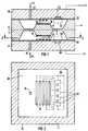
- a capacitive pressure sensorcontains a Si body 6 which is provided with an electrode 16 and can be deflected relative to a fixed silicon (Si) base body 8.
- the Si body 6is designed as part of a Si membrane 4 and is Membrane 4 connected to a support frame 2.
- the Si body 6is formed by a thickening in the central region of the Si membrane 4 and has a flat side facing the Si base body 8 and oriented parallel to the plane spanned by the Si membrane 4.
- the electrode 16is arranged on this flat side.
- the thickeningcauses deflection of the Si membrane 4, the electrode 16 is only displaced essentially parallel to the direction of the deflection.
- the mechanical properties of the membrane 4are not influenced by the electrode 16.
- the support frame 2, the membrane 4 and the body 6are preferably made of monocrystalline silicon with a (100) surface.
- Membrane 4 and body 6can then be produced by anisotropic etching, for example with a mixture of ethylenediamine and pyrocatechol EDP or potassium hydroxide KOH.
- the flanks between the membrane 4 and the body 6 and the support frame 2are then formed by (111) surfaces, so that a membrane 4 results in the shape of a rectangular frame, over which in the center of the body 6 as a base in the form of a Truncated pyramid rises.
- an electrode 16which is vapor-deposited on the body 6 and is made of aluminum Al, for example, is shown.
- the support frame 2, the membrane 4 and the body 6can, however, also consist of highly doped silicon, so that an electrode which is specially vapor-deposited on the surface of the body 6 is not required.
- the support frame 2is applied vacuum-tight to the base body 8 made of silicon via an insulator layer 20, for example silicon dioxide SiO2 or silicon nitride Si3N4.
- the base body 8is provided with a passage opening 14, via which a pressure P1 to be measured, for example is transferred to the membrane 4 by an incompressible fluid.
- These capacitorsare part of a ring oscillator 30 formed from an odd number of inverters, which is preferably also integrated in the base body 8 made of silicon. This measure ensures that the etching processes for producing the membrane 4 and the technological processes for integrating the ring oscillator circuit can take place on different wafers.
- a differential pressure sensor with a symmetrical structurein which the support frame 2, the membrane 4 and the body 6 are designed, for example, mirror-symmetrically to a plane of symmetry 9 running parallel to the plane of the membrane 4.
- the body 6then has the shape of two truncated pyramids.
- the support frame 2is arranged between the base body 8 and a cover plate 10, which is also provided with a passage opening 12 through which the membrane can be pressurized with a pressure P2.
- the space between cover plate 10 and membrane 4is evacuated.
- a membrane 4 with a thickness of about 50 »m and a frame width of about 1 mmis provided for a pressure sensor for the measuring range 104 Pa.
- the base area of the truncated pyramid-shaped body 6 in this exampleis approximately 4 ⁇ 4 mm 2 and the distance between the electrode 16 and the electrodes 24 is approximately 5 to 10 ⁇ m.
- the body 6 and the cover plate 10are also provided on their mutually facing flat sides with electrodes 18 and 26, which also form capacitors which are connected to a further ring oscillator 32.
- This ring oscillator 32is preferably also integrated in a cover plate 10 made of silicon.
- the ring oscillators 30 and 32are each formed by an odd number of inverters, preferably each corresponding to the number of electrodes 24 and 26, respectively. In the preferred embodiment of the figure, the number of electrodes 24 does not match the number of electrodes 26. For example, 5 electrodes 24 and 3 electrodes 26 can be provided. This measure ensures that the ring oscillators 30 and 32 oscillate at different fundamental frequencies, so that undesired couplings are suppressed.
- These changes in capacitythus lead to an opposite dependence of the output frequencies f30 and f32 of the ring oscillators 30 and 32 on the deflection.
- the ring oscillators 30 and 32can also be arranged on the surface of the base body 8 as separate hybrid chips 30 'and 32' shown in broken lines in the figure.
- the chips 30 'and 32'are glued to the surface, for example, and bonded or soldered to corresponding contact pads of the electrodes 24 and 26, respectively. This measure enables the technologically complex IC manufacturing process to be carried out on a separate Si wafer with better utilization of the wafer area.
- Figure 2shows an arrangement of the electrodes 24 on the base body 8 in a plan view.
- the ring oscillator 30,which is made up of a number of inverters 34 corresponding to the number of electrodes 24, is integrated in the base body 8.
- the inverters 3can be produced both in MOS technology or in bipolar technology.
- the conductor tracks, which lead from the electrodes 24 to the inverter outputs, and the inverters 34are shown in dashed lines in the figure.
- a ring oscillatoris provided in a preferred embodiment, which contains an odd number of CMOS inverters 34, each of which contains a p-channel transistor 36 and an n-channel transistor 38.
- Each inverter outputis connected to an electrode 24, so that in each case a capacitor consisting of an electrode 24 and the electrode 16 at ground potential with the capacitance C m is connected to ground at the inverter outputs.
- the capacitance C m of these capacitorsin each case influences the gate delay time of the inverter 34 assigned to it and thus the frequency of the ring oscillator. Since this capacitance C m depends on the deflection of the body carrying the electrodes 16, the mechanical deflection of the body is converted directly into a frequency change at the output A of the ring oscillator.
- the capacitances C mare also connected in parallel with parasitic capacitances C s , which are produced by the capacitors formed in each case between the base body 8 (FIG. 1) and the electrodes 24.
- parasitic capacitances C sare undesirable because they reduce the sensitivity of the pressure sensor.
- the electrodes assigned to the base bodyare arranged in or on an at least partially self-supporting insulator layer above the base body in all embodiments.
- the recesses to be provided in the embodiment according to FIG. 1 corresponding to the embodiments described below according to FIGS. 4 and 5 in the base body 8 in an area below the electrodes 24 and in the cover plate 10 in an area below the electrodes 26are shown in FIG 1 not shown.
- the electrodes 28 assigned to the base body 8are supported on an insulator layer 20 on truncated pyramid-shaped bases 82a, b, c, d.
- FIG. 5shows a sectional view of a surface section running parallel to the surface of the base body 8 provided with the electrodes 28.
- the insulator layer 20is supported on the base body 8 in a self-supporting manner via a plurality of bases and is provided with a plurality of slots 50, for example running in the [100] direction. These slots are required to undercut the insulation layer 20 and allow the anisotropic etchant to attack the silicon substrate of the base plate 8.
- the electrodes 28which were structured beforehand and are shown in broken lines in the figure extend essentially parallel to the slots in the example of the figure 50 and are electrically insulated from one another by the slots 50 and the insulation layer 20 connected via the base 82. In this example, there is no electrode 28 directly above the base. These measures largely reduce the parasitic capacitances C s .
- the dimensions of the pyramid-shaped base 82depend on the duration of exposure to the anisotropic etchant and become smaller as the etching process progresses. In a further embodiment of the invention, the etching process is continued to such an extent that these bases 82 also disappear and a self-supporting insulator layer 20 results, which is only connected to the base body 8 at its outer edges. The electrodes 28 are then free over the Base body 8 arranged and can also be freely designed in terms of their geometric shape.
Landscapes
- Physics & Mathematics (AREA)
- General Physics & Mathematics (AREA)
- Engineering & Computer Science (AREA)
- Power Engineering (AREA)
- Measuring Fluid Pressure (AREA)
- Pressure Sensors (AREA)
Description
Translated fromGermanDie Erfindung bezieht sich auf einen kapazitiven Sensor gemäß dem Oberbegriff des Anspruchs 1.The invention relates to a capacitive sensor according to the preamble of claim 1.
Bei kapazitiven Sensoren wird durch Einwirkung einer Meßgröße die Kapazität eines Meßkondensators verändert. Diese Kapazitätsänderung dient als Maß für die zu erfassende Meßgröße. Die Kapazitätsänderung kann abhängig von den Eigenschaften dieser Meßgröße verschiedene Ursachen haben.In the case of capacitive sensors, the capacitance of a measuring capacitor is changed by the action of a measured variable. This change in capacitance serves as a measure of the measured variable to be recorded. The change in capacitance can have different causes depending on the properties of this measured variable.
Zur Messung mechanischer Größen, beispielsweise Kraft, Druck oder Beschleunigung, eignen sich insbesondere kapazitive Sensoren, bei denen unter der Wirkung der zu messenden Größe ein mit Elektroden versehener Körper relativ zu einer anderen Elektrode mechanisch ausgelenkt und die damit verbundene Kapazitätsänderung erfaßt wird. Kapazitive Sensoren zur Messung mechanischer Größen haben dabei gegenüber piezoresistiven Sensoren, bei denen eine mechanische Auslenkung eines Körpers durch eine damit verbundene Änderung des Spannungszustandes von auf oder in diesem Körper angeordneten Silizium-Widerständen erfaßt wird, den Vorteil einer geringeren Temperaturabhängigkeit und einer höheren Empfindlichkeit.Capacitive sensors are particularly suitable for measuring mechanical quantities, for example force, pressure or acceleration, in which, under the effect of the quantity to be measured, a body provided with electrodes is mechanically deflected relative to another electrode and the associated change in capacitance is detected. Compared to piezoresistive sensors, in which a mechanical deflection of a body is detected by an associated change in the voltage state of silicon resistors arranged on or in this body, capacitive sensors for measuring mechanical quantities have the advantage of a lower temperature dependence and a higher sensitivity.
In der modernen Meßtechnik sind insbesondere solche Sensoren von Vorteil, die eine zu erfassende Meßgröße in ein frequenzanaloges elektrisches Ausgangssignal umwandeln. Frequenzsignale können weitgehend störungsfrei übertragen werden und sind ohne nachfolgende Analog-Digital-Wandlung zur digitalen Weiterverarbeitung geeignet.In modern measurement technology, sensors are particularly advantageous which convert a measurement variable to be detected into a frequency-analog electrical output signal. Frequency signals can largely be transmitted without interference are and are suitable for digital processing without subsequent analog-digital conversion.
Um aus einer Kapazitätsänderung durch eine Meßgröße ein frequenzanaloges Ausgangssignal zu erzeugen, ist bei einer bekannten Ausführungsform eines kapazitiven Strömungssensors für ein Kühlmittel die Meßkapazität des Sensors zusammen mit einer weiteren, fest vorgegebenen Kapazität und mehreren Widerständen und Invertern in einer Ringoszillatorschaltung zusammengeschaltet. Die Schwingungsfrequenz dieses Ringoszillators ändert sich mit der Meßkapazität und ist damit ein Maß für die in einer Kühlmittelleitung fließende Kühlmittelmenge als Meßgröße (US 4 344 293).In order to generate a frequency-analog output signal from a change in capacitance by means of a measured variable, in a known embodiment of a capacitive flow sensor for a coolant the measuring capacitance of the sensor is interconnected in a ring oscillator circuit together with a further, predetermined capacitance and several resistors and inverters. The oscillation frequency of this ring oscillator changes with the measuring capacity and is therefore a measure of the quantity of coolant flowing in a coolant line as a measured variable (US Pat. No. 4,344,293).
Bei einer weiteren bekannten Ausführungsform eines kapazitiven Sensors sind mehrere gleiche Meßkondensatoren als frequenzbestimmende Elemente zusammen mit einer gleichen Anzahl von Invertern in einem Ringoszillator geschaltet. Jede Meßkapazität ist dabei abhängig von derselben Meßgröße und ist genau einem Inverter des Ringoszillators zugeordnet. Es können auch mehrere solche Ringoszillatoren vorgesehen sein. Aus den frequenzanalogen Signalen der Ringoszillatoren wird mit Hilfe eines digitalen Zählers ein digitales Ausgangssignal für die zu bestimmende Meßgröße hergeleitet. Die Meßkondensatoren und die anderen Bestandteile des Ringoszillators sind dabei separat als diskrete Bauteile realisiert (Patent Abstracts of Japan, Vol. 10, No. 106, P-449, Seite 2163, 22. April 1986 und JP-A-60 238715).In a further known embodiment of a capacitive sensor, several identical measuring capacitors are connected as frequency-determining elements together with an identical number of inverters in a ring oscillator. Each measuring capacitance is dependent on the same measured variable and is assigned to exactly one inverter of the ring oscillator. Several such ring oscillators can also be provided. A digital output signal for the measured variable to be determined is derived from the frequency-analog signals of the ring oscillators with the aid of a digital counter. The measuring capacitors and the other components of the ring oscillator are implemented separately as discrete components (Patent Abstracts of Japan, Vol. 10, No. 106, P-449, page 2163, April 22, 1986 and JP-A-60 238715).
Es ist ferner ein in Silizium integrierter kapazitiver Drucksensor mit frequenzanalogem Ausgang bekannt, bei dem eine auf einer Silizium-Membran angeordnete gemeinsame erste Elektrode mit einer zweiten und dritten Elektrode jeweils einen Meßkondensator bildet. Die zweite und dritte Elektrode sind spiegelbildlich zueinander bezüglich einer Symmetrieebene angeordnet, die senkrecht auf der Oberfläche der Silizium-Membran steht und die erste Elektrode in zwei gleiche Hälften teilt. Die Meßkapazitäten der beiden Meßkondensatoren ändern sich somit in gleicher Weise mit dem auf die Membran einwirkenden Druck. Die beiden gleichen Meßkapazitäten sind als frequenzbestimmende Elemente in einen einfachen Wien-Robinson-Oszillator geschaltet, dessen Frequenz von einer der beiden Meßkapazitäten abhängt und als frequenzanaloges Signal für den Druck ausgewertet wird (EP-A-0 195 985).Furthermore, a capacitive pressure sensor with frequency-analog output integrated in silicon is known, in which a common first electrode arranged on a silicon membrane with a second and third electrode each forms a measuring capacitor. The second and third electrodes are arranged in mirror image to one another with respect to a plane of symmetry that is perpendicular to the surface of the silicon membrane and divides the first electrode into two equal halves. The measuring capacities of the two measuring capacitors thus change in the same way with the pressure acting on the membrane. The two same measuring capacitors are connected as frequency-determining elements in a simple Wien-Robinson oscillator, the frequency of which depends on one of the two measuring capacitors and is evaluated as a frequency-analog signal for the pressure (EP-A-0 195 985).
Der Erfindung liegt nun die Aufgabe zugrunde, einen kapazitiven Sensor mit frequenzanalogem Ausgang und mit mehreren Kondensatoren als frequenzbestimmenden Elementen, deren Kapazitäten von einer Meßgröße abhängen und denen jeweils ein Inverter eines Ringoszillators mit einer ungeraden Anzahl von Invertern zugeordnet ist, als in Silizium gefertigten, miniaturisierbaren Drucksensor weiterzubilden, bei dem parasitäre Kapazitäten weitgehend unterdrückt werden.The invention is based on the object, a capacitive sensor with a frequency-analog output and with several capacitors as frequency-determining elements, the capacitances of which depend on a measured variable and to which an inverter of a ring oscillator with an odd number of inverters is assigned, as miniaturized in silicon To further develop pressure sensor in which parasitic capacitances are largely suppressed.
Die genannte Aufgabe wird gelöst mit den Merkmalen des Anspruchs 1.The stated object is achieved with the features of claim 1.
Der kapazitive Sensor enthält einen durch den Druck relativ zu einem Grundkörper aus Silizium auslenkbaren Körper, der durch eine zentrale Verdickung einer Silizium-Membran gebildet wird. Auf dem Silizium-Grundkörper sind mehrere Elektroden angeordnet, die zusammen mit dem auslenkbaren Silizium-Körper jeweils einen Meßkondensator bilden. Dieser Sensor kann mit Hilfe der hochentwickelten Silizium-Mikrostrukturtechnik besonders leicht hergestellt und strukturiert werden.The capacitive sensor contains a body which can be deflected by the pressure relative to a base body made of silicon and which is formed by a central thickening of a silicon membrane. On the silicon body several electrodes are arranged, which together with the deflectable silicon body each form a measuring capacitor. This sensor can be manufactured and structured particularly easily with the aid of the highly developed silicon microstructure technology.
Zur Verringerung von Streukapazitäten sind die Elektroden auf oder in einer wenigstens teilweise freitragenden Isolatorschicht über dem Silizium-Grundkörper angeordnet. Dadurch wird die Kapazität zwischen den Elektroden und dem Grundkörper verringert und die Empfindlichkeit des Sensors erhöht. Zur Erhöhung der mechanischen Stabilität ist die Isolatorschicht vorzugsweise auf mehreren Sockeln abgestützt.To reduce stray capacitance, the electrodes are arranged on or in an at least partially self-supporting insulator layer above the silicon base body. This reduces the capacitance between the electrodes and the base body and increases the sensitivity of the sensor. To increase the mechanical stability, the insulator layer is preferably supported on several bases.
Der Ringoszillator kann vorzugsweise in den Silizium-Grundkörper integriert werden. Die zur Herstellung des auslenkbaren Körpers in der mikromechanischen Technologie erforderlichen Ätzschritte sowie die zur Herstellung des für die Ringoszillatoren erforderlichen integrierten Schaltkreises können dann auf unterschiedlichen Silizium-Wafern erfolgen. Dadurch entfallen beispielsweise zusätzliche Prozeßschritte, die erforderlich sind, um die in den Silizium-Wafer integrierten elektronischen Schaltkreise vor den zur mechanischen Strukturierung erforderlichen Ätzprozessen zu schützen.The ring oscillator can preferably be integrated into the silicon base body. The etching steps required for producing the deflectable body in micromechanical technology and for producing the integrated circuit required for the ring oscillators can then take place on different silicon wafers. This eliminates, for example, additional process steps that are required to protect the electronic circuits integrated in the silicon wafer from the etching processes required for the mechanical structuring.
Es kann außerdem eine zweite Kondensatoranordnung sowie ein ihr zugeordneter zweiter Ringoszillator vorgesehen sein. Dabei sind Kondensatoranordnungen vorteilhaft, bei denen sich eine von der Meßgröße gegenläufige Abhängigkeit der Ausgangsfrequenzen der beiden Ringoszillatoren ergibt. Aus den beiden frequenzanalogen Signalen kann dann eine Differenzfrequenz oder ein Frequenzverhältnis als digitales Signal gebildet werden. Dadurch wird die Empfindlichkeit erhöht und die Abhängigkeit von Störgrößen, wie beispielsweise der Temperatur, verringert.A second capacitor arrangement and a second ring oscillator assigned to it can also be provided. Capacitor arrangements are advantageous in which there is a dependency of the output frequencies of the two ring oscillators on the measured variable. One can then be made from the two frequency-analog signals Differential frequency or a frequency ratio can be formed as a digital signal. This increases the sensitivity and reduces the dependence on disturbance variables, such as the temperature.
Zur weiteren Erläuterung der Erfindung wird auf die Zeichnung verwiesen, in deren
- Figur 1
- ein kapazitiver Drucksensor gemäß der Erfindung schematisch in einem Schnittbild veranschaulicht ist.
Figur 2- zeigt eine Elektrodenanordnung auf einem Grundkörper eines kapazitiven Drucksensors in einer Draufsicht und in
- Figur 3
- ist das Schaltbild einer zum Erzeugen eines frequenzanalogen Ausgangssignals bevorzugten Ringoszillator-Schaltung dargestellt. Anhand der
- Figuren 4 und 5
- wird eine besonders vorteilhafte Ausgestaltung der auf dem Grundkörper befindlichen Elektrodenanordnung jeweils in einem Schnittbild veranschaulicht.
- Figure 1
- a capacitive pressure sensor according to the invention is schematically illustrated in a sectional view.
- Figure 2
- shows an electrode arrangement on a base body of a capacitive pressure sensor in a plan view and in
- Figure 3
- the circuit diagram of a preferred ring oscillator circuit for generating a frequency-analog output signal is shown. Based on
- Figures 4 and 5
- A particularly advantageous embodiment of the electrode arrangement located on the base body is illustrated in each case in a sectional view.
Gemäß Figur 1 enthält ein kapazitiver Drucksensor einen mit einer Elektrode 16 versehenen und relativ zu einem feststehenden Silizium(Si)-Grundkörper 8 auslenkbaren Si-Körper 6. Der Si-Körper 6 ist als Teil einer Si-Membran 4 ausgebildet und über diese Si-Membran 4 mit einem Stützrahmen 2 verbunden. Der Si-Körper 6 wird durch eine Verdickung im zentralen Bereich der Si-Membran 4 gebildet und hat eine dem Si-Grundkörper 8 zugewandte, parallel zu der durch die Si-Membran 4 aufgespannten Ebene orientierte Flachseite. Auf dieser Flachseite ist die Elektrode 16 angeordnet. Durch die Verdickung wird bewirkt, daß bei einer Auslenkung der Si-Membran 4 die Elektrode 16 im wesentlichen nur parallel zur Richtung der Auslenkung verschoben wird. Außerdem werden die mechanischen Eigenschaften der Membran 4 nicht durch die Elektrode 16 beeinflußt.According to FIG. 1, a capacitive pressure sensor contains a
Der Stützrahmen 2, die Membran 4 und der Körper 6 bestehen vorzugsweise aus monokristallinem Silizium mit einer (100)-Oberfläche. Membran 4 und Körper 6 können dann durch anisotropes Ätzen, beispielsweise mit einer Mischung aus Ethylendiamin und Pyrocatechol EDP oder Kaliumhydroxid KOH, hergestellt werden. Die Flanken zwischen der Membran 4 und dem Körper 6 sowie dem Stützrahmen 2 werden dann durch (111)-Flächen gebildet, so daß sich eine Membran 4 in Gestalt eines rechteckigen Rahmens ergibt, über den sich im Zentrum der Körper 6 als Sockel in Gestalt eines Pyramidenstumpfes erhebt.The
Im Beispiel der Figur ist eine auf dem Körper 6 aufgedampfte und beispielsweise aus Aluminium Al bestehende Elektrode 16 dargestellt. Der Stützrahmen 2, die Membran 4 und der Körper 6 können jedoch auch aus hochdotiertem Silizium bestehen, so daß eine eigens auf die Oberfläche des Körpers 6 aufgedampfte Elektrode nicht erforderlich ist.In the example of the figure, an
Der Stützrahmen 2 ist über eine Isolatorschicht 20, beispielsweise Siliziumdioxid SiO₂ oder Siliziumnitrid Si₃N₄, vakuumdicht auf den aus Silizium bestehenden Grundkörper 8 aufgebracht.The
Der Grundkörper 8 ist mit einer Durchlaßöffnung 14 versehen, über die ein zu messender Druck P1 beispielsweise durch ein inkompressibles Fluid auf die Membran 4 übertragen wird.The
Auf der Isolierschicht 20 des Grundkörpers 8 sind gegenüber der Elektrode 16 vorzugsweise mehrere Elektroden 24 angeordnet, die voneinander elektrisch isoliert sind und zusammen mit der Elektrode 16 eine ungerade Anzahl, beispielsweise 5, Kondensatoren bilden. Diese Kondensatoren sind Bestandteil eines aus einer ungeraden Anzahl von Invertern gebildeten Ringoszillators 30, der vorzugsweise ebenfalls in den aus Silizium bestehenden Grundkörper 8 integriert ist. Durch diese Maßnahme wird erreicht, daß die Ätzprozesse zur Herstellung der Membran 4 und die technologischen Prozesse zur Integration des Ringoszillator-Schaltkreises auf unterschiedlichen Wafern stattfinden können.A plurality of
Im Beispiel der Figur ist ein Differenzdruck-Sensor mit symmetrischem Aufbau veranschaulicht, bei dem der Stützrahmen 2, die Membran 4 und der Körper 6 eine beispielsweise spiegelsymmetrisch zu einer parallel zur Ebene der Membran 4 verlaufenden Symmetrieebene 9 gestaltet ist. Der Körper 6 hat dann die Form zweier zusammengesetzter Pyramidenstumpfe. Der Stützrahmen 2 ist zwischen dem Grundkörper 8 und einer Deckplatte 10 angeordnet, die ebenfalls mit einer Durchlaßöffnung 12 versehen ist, über die die Membran mit einem Druck P2 beaufschlagt werden kann. Bei einem entsprechenden Absolutdruck-Sensor ist der Raum zwischen Deckplatte 10 und Membran 4 evakuiert. In einem Ausführungsbeispiel ist bei einem Drucksensor für den Meßbereich 10⁴ Pa eine Membran 4 mit einer Dicke von etwa 50 »m und einer Rahmenbreite von etwa 1 mm vorgesehen. Die Grundfläche des pyramidenstumpfförmigen Körpers 6 beträgt in diesem Beispiel etwa 4 x 4 mm² und der Abstand zwischen der Elektrode 16 und den Elektroden 24 beträgt etwa 5 bis 10 »m.In the example of the figure, a differential pressure sensor with a symmetrical structure is illustrated, in which the
Der Körper 6 und die Deckplatte 10 sind auf ihren einander zugewandten Flachseiten ebenfalls mit Elektroden 18 bzw. 26 versehen, die ebenfalls Kondensatoren bilden, die einem weiteren Ringoszillator 32 zugeschaltet sind. Dieser Ringoszillator 32 ist vorzugsweise ebenfalls in eine aus Silizium bestehende Deckplatte 10 integriert. Die Ringoszillatoren 30 und 32 werden jeweils durch eine ungerade, vorzugsweise jeweils der Anzahl der Elektroden 24 bzw. 26 entsprechenden Anzahl von Invertern gebildet. Im bevorzugten Ausführungsbeispiel der Figur stimmt die Zahl der Elektroden 24 mit der Zahl der Elektroden 26 nicht überein. So können beispielsweise 5 Elektroden 24 und 3 Elektroden 26 vorgesehen sein. Durch diese Maßnahme wird erreicht, daß die Ringoszillatoren 30 und 32 mit unterschiedlichen Grundfrequenzen schwingen, so daß unerwünschte Kopplungen unterdrückt werden.The
Eine Auslenkung der Membran 4, im Beispiel der Figur nach oben wenn der Druck P1 größer als der Druck P2 ist, bewirkt jeweils eine Verringerung der Kapazität der von den Elektroden 16 und 24 gebildeten Kondensatoren und jeweils eine Vergrößerung der Kapazität der von den Elektroden 18 und 26 gebildeten Kondensatoren. Diese Kapazitätsänderungen führen somit zu einer gegenläufigen Abhängigkeit der Ausgangsfrequenzen f₃₀ und f₃₂ der Ringoszillatoren 30 bzw. 32 von der Auslenkung. Durch Auswertung der Differenzfrequenz oder des Frequenzverhältnisses können sowohl die Empfindlichkeit erhöht als auch die Querempfindlichkeiten verringert werden.A deflection of the membrane 4, in the example of the figure upwards when the pressure P1 is greater than the pressure P2, causes a reduction in the capacitance of the capacitors formed by the
Der im Beispiel der Figur dargestellte spiegelsymmetrische Aufbau des Stützrahmens 2, der Membran 4 und des Körpers 6 ist nicht notwendig, da die Ausgangsfrequenzen f₃₀ und f₃₂ der Ringoszillatoren 30 bzw. 32 weder im nichtausgelenkten Zustand der Membran 4 noch hinsichtlich ihrer betragsmäßigen Abhängigkeit von der Auslenkung der Membran 4 übereinstimmen müssen.The mirror-symmetrical structure of the
Die Ringoszillatoren 30 und 32 können auch als separate, in der Figur gestrichelt eingezeichnete hybride Chips 30′ und 32′ auf der Oberfläche des Grundkörpers 8 angeordnet sein. Die Chips 30′ und 32′ sind beispielsweise auf die Oberfläche geklebt und an entsprechende Kontaktpads der Elektroden 24 bzw. 26 gebondet oder verlötet. Durch diese Maßnahme kann der technologisch aufwendige IC-Herstellungsprozeß auf einem separaten Si-Wafer mit einer besseren Ausnutzung der Wafer-Fläche erfolgen.The ring oscillators 30 and 32 can also be arranged on the surface of the
Figur 2 zeigt eine Anordnung der Elektroden 24 auf dem Grundkörper 8 in einer Draufsicht. Im Grundkörper 8 ist der Ringoszillator 30, der aus einer der Anzahl der Elektroden 24 entsprechenden Anzahl von Invertern 34 aufgebaut ist, integriert. Die Inverter 3 können sowohl in MOS-Technologie oder in bipolarer Technologie hergestellt sein. Die Leiterbahnen, die von den Elektroden 24 zu den Inverterausgängen führen, sowie die Inverter 34 sind in der Figur gestrichelt dargestellt.Figure 2 shows an arrangement of the
Gemäß Figur 3 ist in einer bevorzugten Ausführungsform ein Ringoszillator vorgesehen, der eine ungerade Anzahl von CMOS-Invertern 34 enthält, die jeweils einen p-Kanal-Transistor 36 und einen n-Kanal-Transistor 38 enthalten. Jeder Inverterausgang ist mit einer Elektrode 24 verbunden, so daß jeweils an den Inverterausgängen ein aus einer Elektrode 24 und der auf Massepotential befindlichen Elektrode 16 bestehender Kondensator mit der Kapazität Cm nach Masse geschaltet ist. Die Kapazität Cm dieser Kondensatoren beeinflußt jeweils die Gatterlaufzeit des ihm zugeordneten Inverters 34 und somit die Frequenz des Ringoszillators. Da diese Kapazität Cm von der Auslenkung des die Elektroden 16 tragenden Körpers abhängig ist, wird die mechanische Auslenkung des Körpers direkt in eine Frequenzänderung am Ausgang A des Ringoszillators umgewandelt.According to FIG. 3, a ring oscillator is provided in a preferred embodiment, which contains an odd number of
Den Kapazitäten Cm sind noch parasitäre Kapazitäten Cs parallelgeschaltet, die durch die zwischen dem Grundkörper 8 (Figur 1) und den Elektroden 24 jeweils gebildeten Kondensatoren entsteht. Diese parasitären Kapazitäten Cs sind jedoch unerwünscht, da sie die Empfindlichkeit des Drucksensors verringern.The capacitances Cm are also connected in parallel with parasitic capacitances Cs , which are produced by the capacitors formed in each case between the base body 8 (FIG. 1) and the
Zur Verringerung dieser parasitären Kapazitäten Cs sind in allen Ausführungsformen die dem Grundkörper zugeordneten Elektroden in oder auf einer wenigstens teilweise freitragenden Isolatorschicht über dem Grundkörper angeordnet. (Die in der Ausführungsform gemäß FIG. 1 dazu entsprechend den im folgenden beschriebenen Ausführungsformen gemäß den FIG. 4 und 5 vorzusehenden Ausnehmungen in dem Grundkörper 8 in einem Bereich unterhalb der Elektroden 24 und in der Deckplatte 10 in einem Bereich unterhalb der Elektroden 26 sind in der FIG. 1 nicht dargestellt.)To reduce these parasitic capacitances Cs , the electrodes assigned to the base body are arranged in or on an at least partially self-supporting insulator layer above the base body in all embodiments. (The recesses to be provided in the embodiment according to FIG. 1 corresponding to the embodiments described below according to FIGS. 4 and 5 in the
In einer weiteren Ausführungsform gemäß Figur 4 sind die dem Grundkörper 8 zugeordneten Elektroden 28 über eine Isolatorschicht 20 auf pyramidenstumpfförmigen Sockeln 82a, b, c, d abgestützt.In a further embodiment according to FIG. 4, the
In Figur 5 ist ein Schnittbild eines parallel zu der mit den Elektroden 28 versehene Oberfläche des Grundkörpers 8 verlaufenden Flächenausschnitts dargestellt. Die Isolatorschicht 20 ist über mehrere Sockel freitragend auf dem Grundkörper 8 abgestützt und mit mehreren beispielsweise in [100]-Richtung verlaufenden Schlitzen 50 versehen. Diese Schlitze werden zur Unterätzung der Isolationsschicht 20 benötigt und ermöglichen den Angriff des anisotropen Ätzmittels auf das Siliziumsubstrat der Grundplatte 8. Die vorher geeignet strukturierten Elektroden 28, die in der Figur gestrichelt eingezeichnet sind, erstrecken sich im Beispiel der Figur im wesentlichen parallel zu den Schlitzen 50 und sind voneinander durch die Schlitze 50 und die über den Sockel 82 zusammenhängende Isolationsschicht 20 elektrisch isoliert. Unmittelbar über dem Sockel befindet sich in diesem Beispiel keine Elektrode 28. Durch diese Maßnahmen werden die parasitären Kapazitäten Cs weitgehend verringert.FIG. 5 shows a sectional view of a surface section running parallel to the surface of the
Die Ausmaße der pyramidenförmigen Sockel 82 hängen von der Dauer der Einwirkung des anisotropen Ätzmittels ab und werden bei fortschreitendem Ätzprozeß kleiner. In einer weiteren Ausgestaltung der Erfindung wird der Ätzprozeß soweit fortgeführt, daß auch diese Sockel 82 verschwinden und sich eine freitragende Isolatorschicht 20 ergibt, die nur noch an ihren äußeren Rändern mit dem Grundkörper 8 verbunden ist. Die Elektroden 28 sind dann frei über dem Grundkörper 8 angeordnet und können auch hinsichtlich ihrer geometrischen Form frei gestaltet werden.The dimensions of the pyramid-shaped
Claims (7)
- Capacitive sensor having a frequency output and several capacitors as frequency-determining elements, the respective capacitance Cm of which capacitors depends upon a measurable quantity, there being assigned to each of the capacitors an inverter (34) of a ring oscillator (30) having an uneven number of inverters (34), characterised in thata) the capacitance Cm of the each of the capacitors depends upon a mechanical deflection of a silicon body (6) relative to a silicon base body (8) provided with electrodes (24), whereby this silicon body (6) is formed by a central thickening of a silicon membrane (4) and its mechanical deflection is caused by a pressure which is the measurable quantity, andb) the electrodes (24) are arranged above the silicon base body (8) on or in an insulation layer (20) which is at least partly unsupported.
- Capacitive sensor according to claim 1, characterised in that the ring oscillator (30) is arranged on or in the base body (8).
- Capacitive sensor according to claim 1 or 2, characterised in that the ring oscillator (30) is integrated into the base body (8).
- Capacitive sensor according to claim 1 or 2, characterised in that the ring oscillator is arranged on the base body (8) as a hybrid chip (30′).
- Capacitive sensor according to one of the preceding claims, characterised in that there is provided a further capacitor arrangement (18, 26) containing at least one capacitor having a capacitance dependent upon the measurable quantity, with the capacitor or capacitors of this arrangement being connected, as the frequency-determining element or elements, to a second ring oscillator (32).
- Capacitive sensor according to claim 5, characterised in that capacitor arrangements (16, 24 and 18, 26) are provided so that an opposite dependence of the output frequencies f₃₀ and f₃₂ of the two ring oscillators (30 and 32, respectively) on the measurable quantity results.
- Capacitive sensor according to claim 5 or 6, characterised in that the body (6) is arranged between the base body (8) and a cover plate (10) also provided with electrodes (26).
Applications Claiming Priority (2)
| Application Number | Priority Date | Filing Date | Title |
|---|---|---|---|
| DE4014137 | 1990-05-02 | ||
| DE4014137 | 1990-05-02 |
Publications (2)
| Publication Number | Publication Date |
|---|---|
| EP0455070A1 EP0455070A1 (en) | 1991-11-06 |
| EP0455070B1true EP0455070B1 (en) | 1994-06-22 |
Family
ID=6405605
Family Applications (1)
| Application Number | Title | Priority Date | Filing Date |
|---|---|---|---|
| EP91106333AExpired - LifetimeEP0455070B1 (en) | 1990-05-02 | 1991-04-19 | Capacitive sensor with frequency output |
Country Status (2)
| Country | Link |
|---|---|
| EP (1) | EP0455070B1 (en) |
| DE (1) | DE59101980D1 (en) |
Cited By (7)
| Publication number | Priority date | Publication date | Assignee | Title |
|---|---|---|---|---|
| US6114862A (en)* | 1996-02-14 | 2000-09-05 | Stmicroelectronics, Inc. | Capacitive distance sensor |
| US6180989B1 (en) | 1998-02-17 | 2001-01-30 | Stmicroelectronics, Inc. | Selectively doped electrostatic discharge layer for an integrated circuit sensor |
| US6191593B1 (en) | 1997-12-17 | 2001-02-20 | Stmicroelectronics, Inc. | Method for the non-invasive sensing of physical matter on the detection surface of a capacitive sensor |
| US6320394B1 (en) | 1996-02-14 | 2001-11-20 | Stmicroelectronics S.R.L. | Capacitive distance sensor |
| US6987871B2 (en) | 1997-09-11 | 2006-01-17 | Upek, Inc. | Electrostatic discharge protection of a capacitive type fingerprint sensing array |
| US7239227B1 (en) | 1999-12-30 | 2007-07-03 | Upek, Inc. | Command interface using fingerprint sensor input system |
| DE102006001493A1 (en)* | 2006-01-11 | 2007-07-19 | Austriamicrosystems Ag | MEMS sensor and method of manufacture |
Families Citing this family (13)
| Publication number | Priority date | Publication date | Assignee | Title |
|---|---|---|---|---|
| FR2722878B1 (en)* | 1994-07-22 | 1996-09-06 | Suisse Electronique Microtech | CAPACITIVE TYPE DIFFERENTIAL PRESSURE SENSOR |
| DE4439238A1 (en)* | 1994-11-03 | 1996-05-09 | Telefunken Microelectron | Capacitive acceleration sensor |
| DE69618559T2 (en) | 1996-02-14 | 2002-08-14 | Stmicroelectronics S.R.L., Agrate Brianza | Capacitive distance sensor, especially for capturing fingerprints |
| JP3255273B2 (en)* | 1996-06-26 | 2002-02-12 | 株式会社鷹山 | Sensor circuit |
| GB2318231A (en)* | 1996-10-10 | 1998-04-15 | David Frank Moore | Micromechanical ring oscillator sensor |
| EP0950884B1 (en) | 1998-04-17 | 2004-08-18 | Micronas GmbH | Capacitive sensor |
| DE19847563A1 (en) | 1998-04-17 | 1999-10-28 | Micronas Intermetall Gmbh | Capacitative sensor for pressure determination by deformation of a membrane causing a change in capacitance |
| US6512381B2 (en) | 1999-12-30 | 2003-01-28 | Stmicroelectronics, Inc. | Enhanced fingerprint detection |
| GB2385132A (en)* | 2002-02-12 | 2003-08-13 | Seiko Epson Corp | A capacitance sensor |
| US6948388B1 (en)* | 2003-12-18 | 2005-09-27 | The United States Of America As Represented By The Secretary Of The Navy | Wireless remote sensor |
| US8115497B2 (en) | 2007-11-13 | 2012-02-14 | Authentec, Inc. | Pixel sensing circuit with common mode cancellation |
| US9436338B2 (en) | 2014-12-22 | 2016-09-06 | Microsoft Technology Licensing, Llc | Active matrix capacitive touch sensor |
| DE102018105868A1 (en)* | 2018-03-14 | 2019-09-19 | Endress+Hauser SE+Co. KG | Method for producing a semiconductor-based pressure sensor |
Family Cites Families (3)
| Publication number | Priority date | Publication date | Assignee | Title |
|---|---|---|---|---|
| US4091683A (en)* | 1976-09-27 | 1978-05-30 | Panex, Inc. | Single channel electrical comparative measuring system |
| JPS56119474A (en)* | 1980-02-25 | 1981-09-19 | Nippon Denso Co | Device for responding to refrigerang amount for refrigerant circulating apparatus |
| DE3668499D1 (en)* | 1985-03-27 | 1990-03-01 | Siemens Ag | CAPACITIVE PRESSURE SENSOR. |
- 1991
- 1991-04-19EPEP91106333Apatent/EP0455070B1/ennot_activeExpired - Lifetime
- 1991-04-19DEDE59101980Tpatent/DE59101980D1/ennot_activeExpired - Fee Related
Cited By (10)
| Publication number | Priority date | Publication date | Assignee | Title |
|---|---|---|---|---|
| US6114862A (en)* | 1996-02-14 | 2000-09-05 | Stmicroelectronics, Inc. | Capacitive distance sensor |
| US6320394B1 (en) | 1996-02-14 | 2001-11-20 | Stmicroelectronics S.R.L. | Capacitive distance sensor |
| US6731120B2 (en) | 1996-02-14 | 2004-05-04 | Stmicroelectronics, S.R.L. | Capacitive distance sensor |
| US6998855B2 (en) | 1996-02-14 | 2006-02-14 | Upek, Inc. | Capacitive distance sensor |
| US6987871B2 (en) | 1997-09-11 | 2006-01-17 | Upek, Inc. | Electrostatic discharge protection of a capacitive type fingerprint sensing array |
| US6191593B1 (en) | 1997-12-17 | 2001-02-20 | Stmicroelectronics, Inc. | Method for the non-invasive sensing of physical matter on the detection surface of a capacitive sensor |
| US6180989B1 (en) | 1998-02-17 | 2001-01-30 | Stmicroelectronics, Inc. | Selectively doped electrostatic discharge layer for an integrated circuit sensor |
| US7239227B1 (en) | 1999-12-30 | 2007-07-03 | Upek, Inc. | Command interface using fingerprint sensor input system |
| DE102006001493A1 (en)* | 2006-01-11 | 2007-07-19 | Austriamicrosystems Ag | MEMS sensor and method of manufacture |
| DE102006001493B4 (en)* | 2006-01-11 | 2007-10-18 | Austriamicrosystems Ag | MEMS sensor and method of manufacture |
Also Published As
| Publication number | Publication date |
|---|---|
| EP0455070A1 (en) | 1991-11-06 |
| DE59101980D1 (en) | 1994-07-28 |
Similar Documents
| Publication | Publication Date | Title |
|---|---|---|
| EP0455070B1 (en) | Capacitive sensor with frequency output | |
| DE69925803T2 (en) | MICROMECHANICAL SEMICONDUCTOR ACCELERATION SENSOR | |
| DE4332843C2 (en) | Method for producing a micromechanical device and micromechanical device | |
| DE3741941C2 (en) | ||
| DE69315544T2 (en) | Integrated accelerometer with measuring axis parallel to the substrate | |
| DE4000903C1 (en) | ||
| DE69528284T2 (en) | INTEGRATED RESONANT MICROBALK SENSOR AND TRANSISTOR OSCILLATOR | |
| DE69133193T2 (en) | Method for producing a capacitive detector with three substrates, surrounding regions and a working body (force, acceleration, magnetic) | |
| DE68911294T2 (en) | MICRO WORKED ACCELERATOR. | |
| EP0454883B1 (en) | Capacitive sensor | |
| DE69934620T2 (en) | Method of manufacturing a semiconductor acceleration sensor | |
| EP0720748B1 (en) | Integrated micromechanical sensor device and process for producing it | |
| EP0981755B1 (en) | Acceleration sensor | |
| DE19810534A1 (en) | Multiple axis acceleration sensor | |
| WO1991012507A1 (en) | Integratable capacitative pressure sensor and process for its manufacture | |
| DE19750131C2 (en) | Micromechanical differential pressure sensor device | |
| EP0494143B1 (en) | Device for measuring mechanical forces and dynamic effects | |
| DE2505461A1 (en) | MEASURING SIZE CONVERTER | |
| EP0710843B1 (en) | Capacitive acceleration sensor | |
| DE4309206C1 (en) | Semiconductor device having a force and/or acceleration sensor | |
| DE69209743T2 (en) | Differential capacity structure and method of making it | |
| DE3837883A1 (en) | CAPACITIVE ACCELEROMETER AND METHOD FOR THE PRODUCTION THEREOF | |
| DE69714204T2 (en) | pressure monitor | |
| DE69627970T2 (en) | Pressure sensor with rectangular layers and vertical transducer | |
| DE4419267A1 (en) | Semiconductor acceleration sensor and test method therefor |
Legal Events
| Date | Code | Title | Description |
|---|---|---|---|
| PUAI | Public reference made under article 153(3) epc to a published international application that has entered the european phase | Free format text:ORIGINAL CODE: 0009012 | |
| AK | Designated contracting states | Kind code of ref document:A1 Designated state(s):DE FR GB IT | |
| 17P | Request for examination filed | Effective date:19911127 | |
| 17Q | First examination report despatched | Effective date:19921204 | |
| GRAA | (expected) grant | Free format text:ORIGINAL CODE: 0009210 | |
| AK | Designated contracting states | Kind code of ref document:B1 Designated state(s):DE FR GB IT | |
| REF | Corresponds to: | Ref document number:59101980 Country of ref document:DE Date of ref document:19940728 | |
| ITF | It: translation for a ep patent filed | ||
| GBT | Gb: translation of ep patent filed (gb section 77(6)(a)/1977) | Effective date:19940914 | |
| ET | Fr: translation filed | ||
| PLBE | No opposition filed within time limit | Free format text:ORIGINAL CODE: 0009261 | |
| STAA | Information on the status of an ep patent application or granted ep patent | Free format text:STATUS: NO OPPOSITION FILED WITHIN TIME LIMIT | |
| 26N | No opposition filed | ||
| PGFP | Annual fee paid to national office [announced via postgrant information from national office to epo] | Ref country code:GB Payment date:19960322 Year of fee payment:6 | |
| PGFP | Annual fee paid to national office [announced via postgrant information from national office to epo] | Ref country code:FR Payment date:19960422 Year of fee payment:6 | |
| PGFP | Annual fee paid to national office [announced via postgrant information from national office to epo] | Ref country code:DE Payment date:19960620 Year of fee payment:6 | |
| PG25 | Lapsed in a contracting state [announced via postgrant information from national office to epo] | Ref country code:GB Effective date:19970419 | |
| GBPC | Gb: european patent ceased through non-payment of renewal fee | Effective date:19970419 | |
| PG25 | Lapsed in a contracting state [announced via postgrant information from national office to epo] | Ref country code:FR Free format text:LAPSE BECAUSE OF NON-PAYMENT OF DUE FEES Effective date:19971231 | |
| PG25 | Lapsed in a contracting state [announced via postgrant information from national office to epo] | Ref country code:DE Free format text:LAPSE BECAUSE OF NON-PAYMENT OF DUE FEES Effective date:19980101 | |
| REG | Reference to a national code | Ref country code:FR Ref legal event code:ST | |
| PG25 | Lapsed in a contracting state [announced via postgrant information from national office to epo] | Ref country code:IT Free format text:LAPSE BECAUSE OF NON-PAYMENT OF DUE FEES;WARNING: LAPSES OF ITALIAN PATENTS WITH EFFECTIVE DATE BEFORE 2007 MAY HAVE OCCURRED AT ANY TIME BEFORE 2007. THE CORRECT EFFECTIVE DATE MAY BE DIFFERENT FROM THE ONE RECORDED. Effective date:20050419 |