EP0453785A1 - Method of making multilayer thin film circuit comprising integrated thin film resistors - Google Patents
Method of making multilayer thin film circuit comprising integrated thin film resistorsDownload PDFInfo
- Publication number
- EP0453785A1 EP0453785A1EP91104653AEP91104653AEP0453785A1EP 0453785 A1EP0453785 A1EP 0453785A1EP 91104653 AEP91104653 AEP 91104653AEP 91104653 AEP91104653 AEP 91104653AEP 0453785 A1EP0453785 A1EP 0453785A1
- Authority
- EP
- European Patent Office
- Prior art keywords
- thin
- layer
- conductor
- film resistors
- layers
- Prior art date
- Legal status (The legal status is an assumption and is not a legal conclusion. Google has not performed a legal analysis and makes no representation as to the accuracy of the status listed.)
- Withdrawn
Links
- 239000010409thin filmSubstances0.000titleclaimsabstractdescription48
- 238000004519manufacturing processMethods0.000titleclaimsabstractdescription6
- 239000004020conductorSubstances0.000claimsabstractdescription52
- 238000000034methodMethods0.000claimsabstractdescription35
- 239000000758substrateSubstances0.000claimsabstractdescription14
- 239000010410layerSubstances0.000claimsdescription81
- 239000000463materialSubstances0.000claimsdescription13
- 239000012790adhesive layerSubstances0.000claimsdescription12
- 229920002120photoresistant polymerPolymers0.000claimsdescription12
- 229920001721polyimidePolymers0.000claimsdescription9
- 239000004642PolyimideSubstances0.000claimsdescription8
- UMIVXZPTRXBADB-UHFFFAOYSA-NbenzocyclobuteneChemical compoundC1=CC=C2CCC2=C1UMIVXZPTRXBADB-UHFFFAOYSA-N0.000claimsdescription3
- 238000005530etchingMethods0.000claimsdescription3
- 239000002918waste heatSubstances0.000claimsdescription2
- 238000007669thermal treatmentMethods0.000claims1
- VNNRSPGTAMTISX-UHFFFAOYSA-Nchromium nickelChemical compound[Cr].[Ni]VNNRSPGTAMTISX-UHFFFAOYSA-N0.000description4
- 229910052802copperInorganic materials0.000description4
- 238000009413insulationMethods0.000description4
- 229910001120nichromeInorganic materials0.000description4
- 229910052782aluminiumInorganic materials0.000description2
- 229910052804chromiumInorganic materials0.000description2
- 229910052737goldInorganic materials0.000description2
- 230000017525heat dissipationEffects0.000description2
- 229910052759nickelInorganic materials0.000description2
- 229910052719titaniumInorganic materials0.000description2
- 229910052721tungstenInorganic materials0.000description2
- 239000000919ceramicSubstances0.000description1
- 238000010276constructionMethods0.000description1
- 238000001312dry etchingMethods0.000description1
- ZINJLDJMHCUBIP-UHFFFAOYSA-Nethametsulfuron-methylChemical compoundCCOC1=NC(NC)=NC(NC(=O)NS(=O)(=O)C=2C(=CC=CC=2)C(=O)OC)=N1ZINJLDJMHCUBIP-UHFFFAOYSA-N0.000description1
- 239000002184metalSubstances0.000description1
- 229910052751metalInorganic materials0.000description1
- 239000011241protective layerSubstances0.000description1
- 238000004544sputter depositionMethods0.000description1
Images
Classifications
- H—ELECTRICITY
- H01—ELECTRIC ELEMENTS
- H01L—SEMICONDUCTOR DEVICES NOT COVERED BY CLASS H10
- H01L21/00—Processes or apparatus adapted for the manufacture or treatment of semiconductor or solid state devices or of parts thereof
- H01L21/70—Manufacture or treatment of devices consisting of a plurality of solid state components formed in or on a common substrate or of parts thereof; Manufacture of integrated circuit devices or of parts thereof
- H01L21/702—Manufacture or treatment of devices consisting of a plurality of solid state components formed in or on a common substrate or of parts thereof; Manufacture of integrated circuit devices or of parts thereof of thick-or thin-film circuits or parts thereof
- H01L21/707—Manufacture or treatment of devices consisting of a plurality of solid state components formed in or on a common substrate or of parts thereof; Manufacture of integrated circuit devices or of parts thereof of thick-or thin-film circuits or parts thereof of thin-film circuits or parts thereof
- H—ELECTRICITY
- H05—ELECTRIC TECHNIQUES NOT OTHERWISE PROVIDED FOR
- H05K—PRINTED CIRCUITS; CASINGS OR CONSTRUCTIONAL DETAILS OF ELECTRIC APPARATUS; MANUFACTURE OF ASSEMBLAGES OF ELECTRICAL COMPONENTS
- H05K1/00—Printed circuits
- H05K1/16—Printed circuits incorporating printed electric components, e.g. printed resistor, capacitor, inductor
- H05K1/167—Printed circuits incorporating printed electric components, e.g. printed resistor, capacitor, inductor incorporating printed resistors
- H—ELECTRICITY
- H05—ELECTRIC TECHNIQUES NOT OTHERWISE PROVIDED FOR
- H05K—PRINTED CIRCUITS; CASINGS OR CONSTRUCTIONAL DETAILS OF ELECTRIC APPARATUS; MANUFACTURE OF ASSEMBLAGES OF ELECTRICAL COMPONENTS
- H05K1/00—Printed circuits
- H05K1/02—Details
- H05K1/03—Use of materials for the substrate
- H05K1/0306—Inorganic insulating substrates, e.g. ceramic, glass
- H—ELECTRICITY
- H05—ELECTRIC TECHNIQUES NOT OTHERWISE PROVIDED FOR
- H05K—PRINTED CIRCUITS; CASINGS OR CONSTRUCTIONAL DETAILS OF ELECTRIC APPARATUS; MANUFACTURE OF ASSEMBLAGES OF ELECTRICAL COMPONENTS
- H05K2201/00—Indexing scheme relating to printed circuits covered by H05K1/00
- H05K2201/03—Conductive materials
- H05K2201/0302—Properties and characteristics in general
- H05K2201/0317—Thin film conductor layer; Thin film passive component
- H—ELECTRICITY
- H05—ELECTRIC TECHNIQUES NOT OTHERWISE PROVIDED FOR
- H05K—PRINTED CIRCUITS; CASINGS OR CONSTRUCTIONAL DETAILS OF ELECTRIC APPARATUS; MANUFACTURE OF ASSEMBLAGES OF ELECTRICAL COMPONENTS
- H05K2201/00—Indexing scheme relating to printed circuits covered by H05K1/00
- H05K2201/09—Shape and layout
- H05K2201/09209—Shape and layout details of conductors
- H05K2201/095—Conductive through-holes or vias
- H05K2201/09509—Blind vias, i.e. vias having one side closed
- H05K2201/09518—Deep blind vias, i.e. blind vias connecting the surface circuit to circuit layers deeper than the first buried circuit layer
- H—ELECTRICITY
- H05—ELECTRIC TECHNIQUES NOT OTHERWISE PROVIDED FOR
- H05K—PRINTED CIRCUITS; CASINGS OR CONSTRUCTIONAL DETAILS OF ELECTRIC APPARATUS; MANUFACTURE OF ASSEMBLAGES OF ELECTRICAL COMPONENTS
- H05K2203/00—Indexing scheme relating to apparatus or processes for manufacturing printed circuits covered by H05K3/00
- H05K2203/03—Metal processing
- H05K2203/0361—Stripping a part of an upper metal layer to expose a lower metal layer, e.g. by etching or using a laser
- H—ELECTRICITY
- H05—ELECTRIC TECHNIQUES NOT OTHERWISE PROVIDED FOR
- H05K—PRINTED CIRCUITS; CASINGS OR CONSTRUCTIONAL DETAILS OF ELECTRIC APPARATUS; MANUFACTURE OF ASSEMBLAGES OF ELECTRICAL COMPONENTS
- H05K2203/00—Indexing scheme relating to apparatus or processes for manufacturing printed circuits covered by H05K3/00
- H05K2203/17—Post-manufacturing processes
- H05K2203/171—Tuning, e.g. by trimming of printed components or high frequency circuits
- H—ELECTRICITY
- H05—ELECTRIC TECHNIQUES NOT OTHERWISE PROVIDED FOR
- H05K—PRINTED CIRCUITS; CASINGS OR CONSTRUCTIONAL DETAILS OF ELECTRIC APPARATUS; MANUFACTURE OF ASSEMBLAGES OF ELECTRICAL COMPONENTS
- H05K3/00—Apparatus or processes for manufacturing printed circuits
- H05K3/10—Apparatus or processes for manufacturing printed circuits in which conductive material is applied to the insulating support in such a manner as to form the desired conductive pattern
- H05K3/108—Apparatus or processes for manufacturing printed circuits in which conductive material is applied to the insulating support in such a manner as to form the desired conductive pattern by semi-additive methods; masks therefor
- H—ELECTRICITY
- H05—ELECTRIC TECHNIQUES NOT OTHERWISE PROVIDED FOR
- H05K—PRINTED CIRCUITS; CASINGS OR CONSTRUCTIONAL DETAILS OF ELECTRIC APPARATUS; MANUFACTURE OF ASSEMBLAGES OF ELECTRICAL COMPONENTS
- H05K3/00—Apparatus or processes for manufacturing printed circuits
- H05K3/38—Improvement of the adhesion between the insulating substrate and the metal
- H05K3/388—Improvement of the adhesion between the insulating substrate and the metal by the use of a metallic or inorganic thin film adhesion layer
- H—ELECTRICITY
- H05—ELECTRIC TECHNIQUES NOT OTHERWISE PROVIDED FOR
- H05K—PRINTED CIRCUITS; CASINGS OR CONSTRUCTIONAL DETAILS OF ELECTRIC APPARATUS; MANUFACTURE OF ASSEMBLAGES OF ELECTRICAL COMPONENTS
- H05K3/00—Apparatus or processes for manufacturing printed circuits
- H05K3/46—Manufacturing multilayer circuits
- H05K3/4644—Manufacturing multilayer circuits by building the multilayer layer by layer, i.e. build-up multilayer circuits
- Y—GENERAL TAGGING OF NEW TECHNOLOGICAL DEVELOPMENTS; GENERAL TAGGING OF CROSS-SECTIONAL TECHNOLOGIES SPANNING OVER SEVERAL SECTIONS OF THE IPC; TECHNICAL SUBJECTS COVERED BY FORMER USPC CROSS-REFERENCE ART COLLECTIONS [XRACs] AND DIGESTS
- Y10—TECHNICAL SUBJECTS COVERED BY FORMER USPC
- Y10S—TECHNICAL SUBJECTS COVERED BY FORMER USPC CROSS-REFERENCE ART COLLECTIONS [XRACs] AND DIGESTS
- Y10S428/00—Stock material or miscellaneous articles
- Y10S428/901—Printed circuit
- Y—GENERAL TAGGING OF NEW TECHNOLOGICAL DEVELOPMENTS; GENERAL TAGGING OF CROSS-SECTIONAL TECHNOLOGIES SPANNING OVER SEVERAL SECTIONS OF THE IPC; TECHNICAL SUBJECTS COVERED BY FORMER USPC CROSS-REFERENCE ART COLLECTIONS [XRACs] AND DIGESTS
- Y10—TECHNICAL SUBJECTS COVERED BY FORMER USPC
- Y10T—TECHNICAL SUBJECTS COVERED BY FORMER US CLASSIFICATION
- Y10T29/00—Metal working
- Y10T29/49—Method of mechanical manufacture
- Y10T29/49002—Electrical device making
- Y10T29/49082—Resistor making
- Y10T29/49099—Coating resistive material on a base
- Y—GENERAL TAGGING OF NEW TECHNOLOGICAL DEVELOPMENTS; GENERAL TAGGING OF CROSS-SECTIONAL TECHNOLOGIES SPANNING OVER SEVERAL SECTIONS OF THE IPC; TECHNICAL SUBJECTS COVERED BY FORMER USPC CROSS-REFERENCE ART COLLECTIONS [XRACs] AND DIGESTS
- Y10—TECHNICAL SUBJECTS COVERED BY FORMER USPC
- Y10T—TECHNICAL SUBJECTS COVERED BY FORMER US CLASSIFICATION
- Y10T428/00—Stock material or miscellaneous articles
- Y10T428/24—Structurally defined web or sheet [e.g., overall dimension, etc.]
- Y10T428/24802—Discontinuous or differential coating, impregnation or bond [e.g., artwork, printing, retouched photograph, etc.]
- Y10T428/24917—Discontinuous or differential coating, impregnation or bond [e.g., artwork, printing, retouched photograph, etc.] including metal layer
Definitions
- the inventionis in the field of printed circuit board manufacture and relates to a method according to the preamble of claim 1, with which two-layer or multi-layer thin-film circuits with integrated, trimmable thin-film resistors can be produced.
- a methodwould be advantageous, with the aid of which thin-film resistors can be integrated into multilayer thin-film circuits in such a way that they can be exposed to as high a current load as the resistance material allows with sufficient heat dissipation. To do this, one would have to be able to place the thin-film resistors directly on the heat-dissipating substrate without having to subject them to a subsequent, damaging process step.
- This methodis based on the fact that in the production of the lower layers of the multilayer thin-film circuit closer to the substrate Zones are formed in which thin-film resistors are created after the damaging process steps, for example, only when the uppermost layer, which is furthest from the substrate, is produced. These lie directly on the substrate in these zones and can be trimmed afterwards if necessary.
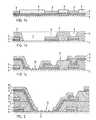
- Typical thicknesses of the layers produced by the process describedare: 0.01 ⁇ m for the adhesive layers 1 or 1 ′, 0.2 ⁇ m for the conductive layers 2 or 2 ′ and 5 ⁇ m for the conductor tracks 3 or 3 ′.
- the thin-film resistor 10 shown in FIG. 1cis connected in the figure on the left side to a conductor of the second (upper) conductor layer, on the right side in the figure to a conductor of the first (lower) conductor layer, between which conductors the resistor is now can be adjusted.
- corresponding windowscan be created with thin-film resistors that are in contact with other conductor layers, for example with the second (upper) conductor layer on both sides.
- a protective layercan be applied over everything.
- more than two-layer thin-film circuitscan also be produced in the manner described, the thin-film resistors always being formed with the uppermost, most distant, layer of the conductor that is built up last, but may be in contact with conductors from any of the conductor layers .
- Figure 2shows a corresponding arrangement of a three-layer thin-film circuit.
- the thin-film resistor 10was created as part of the adhesive layer 3 ′′ of the third (uppermost) conductor layer, the third conductor layer being produced according to the method steps described in connection with FIG. 1c.
- the thin film resistor shownis in contact with the third (top) conductor layer on the left side in the figure, and with the second (middle) conductor layer on the right side in the figure.
- the windowbreaks through both insulating layers 5 and 5 '.
- the method according to the inventioncan be used to produce thin-film resistors which are in contact with any of the conductor layers.
- Similar windows as for thin-film resistorscan also be left open in multilayer thin-film circuits and then equipped with components that generate a lot of waste heat during operation. Such windows can also be created for bond wires and other connections between components and conductors of the lower conductor layers.
Landscapes
- Engineering & Computer Science (AREA)
- Microelectronics & Electronic Packaging (AREA)
- Physics & Mathematics (AREA)
- Condensed Matter Physics & Semiconductors (AREA)
- General Physics & Mathematics (AREA)
- Manufacturing & Machinery (AREA)
- Computer Hardware Design (AREA)
- Power Engineering (AREA)
- Parts Printed On Printed Circuit Boards (AREA)
- Apparatuses And Processes For Manufacturing Resistors (AREA)
Abstract
Description
Translated fromGermanDie Erfindung liegt auf dem Gebiete der Leiterplattenherstellung und betrifft ein Verfahren gemäss dem Oberbegriff des Patentanspruchs 1, mit dem zwei- oder mehrlagige Dünnschichtschaltungen mit integrierten, trimmbaren Dünnschichtwiderständen hergestellt werden können.The invention is in the field of printed circuit board manufacture and relates to a method according to the preamble of
Verfahren zur Herstellung von mehrlagigen Dünnschichtschaltungen sind bekannt zum Beispiel aus der Europäischen Patentanmeldung 0 286 854 (Verfahren zum Herstellen einer mehrlagigen Dünnschichtschaltung). Dieses Verfahren wird hier als bekannt vorausgesetzt.Methods for producing multilayer thin-film circuits are known, for example, from European patent application 0 286 854 (method for producing a multilayer thin-film circuit). This procedure is assumed to be known here.
Mehrlagige Dünnschichtschaltungen weisen heute sehr hohe Leiterbahnendichten und dadurch kurze Verbindungen auf. Erfordert zum Beispiel ein Schaltkreis grosse Speiseströme, die über kurze, breite Leitungen geführt werden müssen, und hohe Leiterbahndichte, wird man vorteilhaft eine mehrlagige Dünnschichtschaltung verwenden. Kommen nun aber als zusätzliche Forderungen genaue, trimmbare Widerstände hinzu, muss eine andere Technik oder eine Mischtechnik angewendet werden, denn in mehrlagige Dünnschichtschaltungen lassen sich bis anhin aus den folgenden Gründen keine Dünnschichtwiderstände integrieren:
- Werden die Widerstände in der dem wärmeableitenden Substrat am nächsten, untersten Lage der Dünnschichtschaltung integriert, müssen nachher darüber eine oder mehrere Isolationsschichten erstellt und bei für den Widerstandswerkstoff zu hohen Temperaturen ausgehärtet werden (z.B. Imidisierung von Polyimidschichten bei 300 bis 400°C).
- Werden die Widerstände in der zweiten oder einer weiteren Lage integriert, sind sie durch mindestens eine Isolationsschicht vom wärmeabführenden Substrat getrennt und können deshalb nicht so belastet werden, wie es bei einer direkten Wärmeabführung durch das Substrat möglich wäre.
- If the resistors are integrated in the lowest layer of the thin-film circuit closest to the heat-dissipating substrate, Afterwards, one or more insulation layers must be created and cured at temperatures that are too high for the resistance material (eg imidization of polyimide layers at 300 to 400 ° C).
- If the resistors are integrated in the second or a further layer, they are separated from the heat-dissipating substrate by at least one insulation layer and therefore cannot be loaded as much as would be possible with direct heat dissipation through the substrate.
Die Anwendungen aber, für die eine solche Kombination von mehrlagigen Dünnschichtschaltungen mit Dünnschichtwiderständen vorteilhaft wären, sind zahlreich. Ein Beispiel dafür sind schnelle Analog/Digitalwandler. Der analoge Teil braucht genaue, trimmbare Widerstände, der digitale Teil benötigt eine hohe Verbindungsdichte und die schnellen Bausteine insgesamt grosse Speiseströme.However, the applications for which such a combination of multilayer thin-film circuits with thin-film resistors would be advantageous are numerous. An example of this are fast analog / digital converters. The analog part needs precise, trimmable resistors, the digital part needs a high connection density and the fast components all in all large feed currents.
Vorteilhaft wäre ein Verfahren, mit dessen Hilfe Dünnschichtwiderstände in mehrlagige Dünnschichtschaltungen so integriert werden können, dass sie einer so hohen Strom-Belastung ausgesetzt werden können, wie es der Widerstandswerkstoff bei ausreichender Wärmeabführung zulässt. Dazu müsste man die Dünnschichtwiderstände direkt auf das wärmeableitende Substrat aufsetzen können, ohne sie nachher einem darauffolgenden, schädigenden Verfahrensschritt unterziehen zu müssen.A method would be advantageous, with the aid of which thin-film resistors can be integrated into multilayer thin-film circuits in such a way that they can be exposed to as high a current load as the resistance material allows with sufficient heat dissipation. To do this, one would have to be able to place the thin-film resistors directly on the heat-dissipating substrate without having to subject them to a subsequent, damaging process step.
Ein solches Verfahren ist im Patentanspruch 1 definiert und wird nun anhand eines Beispiels detailliert beschrieben.Such a method is defined in
Dieses Verfahren basiert darauf, dass bei der Herstellung der unteren, dem Substrat näheren Lagen der mehrlagigen Dünnschichtschaltung Zonen gebildet werden, in denen nach den schädigenden Verfahrensschritten, bspw. erst mit der Herstellung der obersten, vom Substrat am weitesten entfernten Lage Dünnschichtwiderstände erstellt werden. Diese liegen in diesen Zonen direkt auf dem Substrat und können, falls erforderlich, nachträglich getrimmt werden.This method is based on the fact that in the production of the lower layers of the multilayer thin-film circuit closer to the substrate Zones are formed in which thin-film resistors are created after the damaging process steps, for example, only when the uppermost layer, which is furthest from the substrate, is produced. These lie directly on the substrate in these zones and can be trimmed afterwards if necessary.
Zur Illustration der detaillierten Beschreibung des erfindungsgemässen Verfahrens dienen die folgenden Figuren. Sie zeigen:
- Fig. 1:
- einen typischen Verfahrensablauf für das erfindungsgemässe Verfahren und
- Fig. 2:
- ein Beispiel eines nach dem erfindungsgemässen Verfahren hergestellten, in eine dreilagige Dünnschichtschaltung integrierten Dünnschichtwiderstandes.
- Fig. 1:
- a typical procedure for the inventive method and
- Fig. 2:
- an example of a thin-film resistor produced by the method according to the invention and integrated in a three-layer thin-film circuit.
Figur 1 zeigt die Hauptschritte des erfindungsgemässen Verfahrens am Beispiel einer zweilagigen Dünnschichtschaltung:
- 1a:
- Auf ein Keramiksubstrat S wird nach bekannten Methoden eine erste Leiterlage aufgebracht. Zum Beispiel wird ganzflächig eine
Haftschicht 1 gesputtert aus einem oxydationsfreudigen Metall (bspw. Cr, Ti, W, Al, NiCr). Auf dieHaftschicht 1 wird ganzflächig eine Leitschicht 2 (bspw. aus Cu, Ni) gesputtert. Über dieserLeitschicht 2 wird eine Schicht Photolack 4 angebracht und auf photolithographischem Wege zum gewünschten Leiterbild dieser Leiterlage strukturiert. Darauf werden die Leiterbahnen 3 (bspw. aus Cu, Au) selektiv galvanisch aufgebracht. - 1b:
- Die
Photolackschicht 4 wird entfernt. Die nun freigelegten Teile derLeitschicht 2 werden mit einem dem Material dieser Schicht angepassten Ätzmittel weggeätzt. Die dadurch freigelegten Teile derHaftschicht 1 werden dann mit einem dem Material dieser Haftschicht angepassten Ätzmittel wegeätzt. Die ganze erste Leiterlage wird nun mit einer Isolierschicht 5 (z.B. aus negativ-photosensitivem Polyimid) bedeckt. Durch eine dem Material der Isolierschicht entsprechende Methode (z.B. UV-Belichtung durch eine Photomaske und anschliessende Entwicklung) wird die Isolierschicht strukturiert. Die Isolierschicht wird überall dort entfernt, wo Durchkontaktierungen zwischen der bereits erstellten und der darüber liegenden Leiterlage hergestellt werden sollen (Stellen 6) und neu, gemäss dem erfindungsgemässen Verfahren dort, wo für Dünnschichtwiderstände Fenster (Zonen) offengehalten werden sollen (Stellen 7), und dort, wo die zu erstellenden Dünnschichtwiderstände mit Leitern der untersten Lage kontaktiert werden sollen (Stellen 8). Nun wird dieIsolierschicht 5 bei der adäquaten Temperatur polymerisiert. An Stelle photoaktiver Polyimide lassen sich andere Materialien für dieIsolierschichten 5 verwenden, wie zum trockenätzen geeignete Polyimide oder Benzocyclobuten, Polyphenylquinoxalin oder verwandte Materialien. Dabei wird die Isolierschicht zunächst polymerisiert bzw. mit bis zu 400°C gehärtet, mit strukturiertem Aetzresist nach einer gängigen Variante maskiert, anschliessend im Plasma trockengeäzt und schliesslich die Maskierung entfernt. - 1c:
- Eine zweite Leiterlage wird aufgebracht, indem in analoger Weise, wie im Zusammenhang mit Figur 1a beschrieben, eine
Haftschicht 1' zum Beispiel aus NiCr oder TaN und eine Leitschicht 2' ganzflächig gesputtert werden. DieHaftschicht 1' liegt in den im ersten Arbeitsgang offen gelassenen Fenstern direkt auf dem Substrat S und wird dort dieDünnschichtwiderstände 10 bilden. Weiter wird eine Photoresistschicht aufgebracht (in der Figur nicht sichtbar), gemäss den gewünschten Leiterbahnen dieser zweiten Leiterlage strukturiert, die Leiterbahnen 3' galvanisch aufgebracht und die Photoresistschicht entfernt. Die Leiterbahnen der zweiten Leiterlage kontaktieren die Leiterbahnen der ersten Leiterlage: anStellen 6, wo Kontaktierungszonen durch dieIsolierschicht 5 hindurch vorgesehen wurden, und anStellen 8, wo Kontaktierungen der ersten (unteren) Leiterlage mit denDünnschichtwiderständen 10 vorgesehen sind. Nach dem Aufbau der Leiterbahnen 3' der zweiten Leiterlage wird die dazu aufgetragene Photolackschicht entfernt und die freigelegten Teile der Leitschicht 2' wegeätzt. Vor dem Wegätzen der nun freigelegten Teile derHaftschicht 1' (Zonen 7 und 11) wird erneut eine Photolackschicht (in der Figur ebenfalls nicht sichtbar) aufgebracht, in die die Widerstandsstrukturen (Zone 7) eingebracht werden. Dies sind vorteilhafterweise trimmbare Muster, die nachträglich mit Laser fei ngetrimmt werden können. DieHaftschicht 1' wird dann geätzt, wodurch dieDünnschichtwiderstände 10 entstehen.
- 1a:
- A first conductor layer is applied to a ceramic substrate S using known methods. For example, an
adhesive layer 1 is sputtered over the entire surface from a metal that is easy to oxidize (for example Cr, Ti, W, Al, NiCr). A conductive layer 2 (for example made of Cu, Ni) is sputtered over the entire surface of theadhesive layer 1. A layer ofphotoresist 4 is applied over thisconductive layer 2 and structured in a photolithographic way to the desired conductor pattern of this conductor layer. The conductor tracks 3 (for example made of Cu, Au) are selectively electroplated thereon. - 1b:
- The
photoresist layer 4 is removed. The parts of theconductive layer 2 which are now exposed are etched away with an etchant which is adapted to the material of this layer. The parts of theadhesive layer 1 which are thereby exposed are then etched away with an etchant which is adapted to the material of this adhesive layer. The entire first conductor layer is now covered with an insulating layer 5 (for example made of negative photosensitive polyimide). The insulation layer is structured by a method corresponding to the material of the insulation layer (for example UV exposure through a photomask and subsequent development). The insulating layer is removed wherever plated-through holes between the conductor layer already created and the conductor layer above it are to be made (points 6) and new, according to the inventive method, where windows (zones) are to be kept open for thin-film resistors (points 7), and where the thin-film resistors to be created are to be contacted with conductors in the lowest position (positions 8). Now the insulatinglayer 5 is polymerized at the adequate temperature. Instead of photoactive polyimides, other materials can be used for the insulatinglayers 5, such as polyimides or benzocyclobutene suitable for dry etching, polyphenylquinoxaline or related materials. The insulating layer is first polymerized or cured at up to 400 ° C, masked with structured etching resist according to a common variant, then dry-etched in the plasma and finally the mask is removed. - 1c:
- A second conductor layer is applied by sputtering an
adhesive layer 1 ', for example made of NiCr or TaN, and a conductive layer 2' over the entire surface in an analogous manner, as described in connection with FIG. 1a. Theadhesive layer 1 'lies in the windows left open in the first operation directly on the substrate S and will form the thin-film resistors 10 there. Furthermore, a photoresist layer is applied (not visible in the figure), structured according to the desired conductor tracks of this second conductor layer, the conductor tracks 3 ' galvanically applied and the photoresist layer removed. The conductor tracks of the second conductor layer contact the conductor tracks of the first conductor layer: atpoints 6 where contact zones have been provided through the insulatinglayer 5 and atpoints 8 where contacts of the first (lower) conductor layer with thethin film resistors 10 are provided. After the construction of the conductor tracks 3 'of the second conductor layer, the photoresist layer applied for this purpose is removed and the exposed parts of the conductive layer 2' are etched away. Before the now exposed parts of theadhesive layer 1 '(zones 7 and 11) are etched away, a photoresist layer (likewise not visible in the figure) is applied, into which the resistance structures (zone 7) are introduced. These are advantageously trimmable patterns that can be finely trimmed with laser afterwards. Theadhesive layer 1 'is then etched, as a result of which the thin-film resistors 10 are formed.
Typische Dicken der nach dem beschriebenen Verfahren hergestellten Schichten sind: 0,01µm für die Haftschichten 1 oder 1', 0,2µm für die Leitschichten 2 oder 2' und 5µm für die Leiterbahnen 3 oder 3'.Typical thicknesses of the layers produced by the process described are: 0.01 μm for the
Der in der Figur 1c abgebildete Dünnschichtwiderstand 10 ist in der Figur auf der linken Seite mit einem Leiter der zweiten (oberen) Leiterlage, auf der in der Figur rechten Seite mit einem Leiter der ersten (unteren) Leiterlage verbunden, zwischen welchen Leitern der Widerstand nun eingestellt werden kann. In analoger Weise können entsprechende Fenster erstellt werden mit Dünnschichtwiderständen, die mit anderen Leiterlagen kontaktiert sind, bspw. beidseitig mit der zweiten (oberen) Leiterlage. Falls erwünscht, kann zum Schluss noch eine Schutzschicht über alles appliziert werden.The thin-
Mit demselben Verfahren lassen sich in der beschriebenen Weise auch mehr als zweilagige Dünnschichtschaltungen herstellen, wobei die Dünnschichtwiderstände immer mit der obersten, vom Substrat am weitesten entfernten, Leiterlage, die zuletzt aufgebaut wird, entstehen, aber mit Leitern aus irgend einer der Leiterlagen kontaktiert sein können.With the same method, more than two-layer thin-film circuits can also be produced in the manner described, the thin-film resistors always being formed with the uppermost, most distant, layer of the conductor that is built up last, but may be in contact with conductors from any of the conductor layers .
Figur 2 zeigt eine entsprechende Anordnung einer dreilagigen Dünnschichtschaltung. Der Dünnschichtwiderstand 10 ist in diesem Falle als Teil der Haftschicht 3'' der dritten (obersten) Leiterlage entstanden, wobei die dritte Leiterlage nach den im Zusammenhang mit Figur 1c beschriebenen Verfahrensschritten hergestellt wird. Der abgebildete Dünnschichtwiderstand ist auf der in der Figur linken Seite mit der dritten (obersten) Leiterlage, auf der in der Figur rechten Seite mit der zweiten (mittleren) Leiterlage kontaktiert. Das Fenster durchbricht beide Isolierschichten 5 und 5'.Figure 2 shows a corresponding arrangement of a three-layer thin-film circuit. In this case, the thin-
Auch im Falle von mehr als zweilagigen Dünnschichtschaltungen können mit dem erfindungsgemässen Verfahren Dünnschichtwiderstände erstellt werden, die mit irgend einer der Leiterlagen kontaktiert sind.Even in the case of more than two-layer thin-film circuits, the method according to the invention can be used to produce thin-film resistors which are in contact with any of the conductor layers.
Ähnliche Fenster wie für Dünnschichtwiderstände können in mehrlagigen Dünnschichtschaltungen auch offen gelassen und dann mit Komponenten, die im Betrieb viel Abwärme erzeugen, bestückt werden. Auch für Bonddrähte und andere Verbindungen zwischen Komponenten und Leitern der unteren Leiterlagen können solche Fenster erstellt werden.Similar windows as for thin-film resistors can also be left open in multilayer thin-film circuits and then equipped with components that generate a lot of waste heat during operation. Such windows can also be created for bond wires and other connections between components and conductors of the lower conductor layers.
Claims (7)
Translated fromGermanApplications Claiming Priority (2)
| Application Number | Priority Date | Filing Date | Title |
|---|---|---|---|
| CH378/90 | 1990-02-06 | ||
| CH137890 | 1990-04-24 |
Publications (1)
| Publication Number | Publication Date |
|---|---|
| EP0453785A1true EP0453785A1 (en) | 1991-10-30 |
Family
ID=4209025
Family Applications (1)
| Application Number | Title | Priority Date | Filing Date |
|---|---|---|---|
| EP91104653AWithdrawnEP0453785A1 (en) | 1990-04-24 | 1991-03-25 | Method of making multilayer thin film circuit comprising integrated thin film resistors |
Country Status (2)
| Country | Link |
|---|---|
| US (1) | US5227012A (en) |
| EP (1) | EP0453785A1 (en) |
Families Citing this family (43)
| Publication number | Priority date | Publication date | Assignee | Title |
|---|---|---|---|---|
| JPH05129760A (en)* | 1991-11-06 | 1993-05-25 | Fujitsu Ltd | Method of forming conductor pattern |
| US5355014A (en)* | 1993-03-03 | 1994-10-11 | Bhasker Rao | Semiconductor device with integrated RC network and Schottky diode |
| US5370766A (en)* | 1993-08-16 | 1994-12-06 | California Micro Devices | Methods for fabrication of thin film inductors, inductor networks and integration with other passive and active devices |
| JPH07131155A (en)* | 1993-11-01 | 1995-05-19 | Hitachi Ltd | Method for manufacturing multilayer wiring board and multilayer wiring board |
| US5965065A (en)* | 1994-12-05 | 1999-10-12 | Powell; Stephen Forbes | Method of filtering x-rays |
| JP2917867B2 (en)* | 1995-08-14 | 1999-07-12 | 日本電気株式会社 | Multilayer wiring board |
| KR100272850B1 (en)* | 1995-10-23 | 2001-01-15 | 엔도 마사루 | Resin filler and multilayer printed wiring board |
| US6010768A (en) | 1995-11-10 | 2000-01-04 | Ibiden Co., Ltd. | Multilayer printed circuit board, method of producing multilayer printed circuit board and resin filler |
| US5863446A (en)* | 1996-11-08 | 1999-01-26 | W. L. Gore & Associates, Inc. | Electrical means for extracting layer to layer registration |
| US5976392A (en)* | 1997-03-07 | 1999-11-02 | Yageo Corporation | Method for fabrication of thin film resistor |
| US6787047B1 (en)* | 1997-03-13 | 2004-09-07 | Robert Bosch Gmbh | Methods for manufacturing a microstructured sensor |
| US5903525A (en)* | 1997-04-18 | 1999-05-11 | Read-Rite Corporation | Coil for use with magneto-optical head |
| US5978319A (en)* | 1997-11-06 | 1999-11-02 | Read-Rite Corporation | Thin electro-magnetic coil assembly for attachment to a slider |
| MY139405A (en)* | 1998-09-28 | 2009-09-30 | Ibiden Co Ltd | Printed circuit board and method for its production |
| US6303423B1 (en) | 1998-12-21 | 2001-10-16 | Megic Corporation | Method for forming high performance system-on-chip using post passivation process |
| US8178435B2 (en)* | 1998-12-21 | 2012-05-15 | Megica Corporation | High performance system-on-chip inductor using post passivation process |
| US7531417B2 (en)* | 1998-12-21 | 2009-05-12 | Megica Corporation | High performance system-on-chip passive device using post passivation process |
| US7381642B2 (en)* | 2004-09-23 | 2008-06-03 | Megica Corporation | Top layers of metal for integrated circuits |
| US6965165B2 (en) | 1998-12-21 | 2005-11-15 | Mou-Shiung Lin | Top layers of metal for high performance IC's |
| US6495442B1 (en)* | 2000-10-18 | 2002-12-17 | Magic Corporation | Post passivation interconnection schemes on top of the IC chips |
| US6229181B1 (en) | 1999-04-30 | 2001-05-08 | Digital Devices, Inc. | Semiconductor device and method of forming a semiconductor structure to provide electrostatic discharge protection |
| US6262442B1 (en)* | 1999-04-30 | 2001-07-17 | Dmitri G. Kravtchenko | Zener diode and RC network combination semiconductor device for use in integrated circuits |
| US6542379B1 (en)* | 1999-07-15 | 2003-04-01 | International Business Machines Corporation | Circuitry with integrated passive components and method for producing |
| DE60041314D1 (en)* | 1999-11-10 | 2009-02-26 | Boeing Co | Manufacturing method for thin-film components |
| US6404615B1 (en) | 2000-02-16 | 2002-06-11 | Intarsia Corporation | Thin film capacitors |
| US20050148271A1 (en)* | 2000-02-25 | 2005-07-07 | Si Diamond Technology, Inc. | Nanotubes cold cathode |
| US6486530B1 (en) | 2000-10-16 | 2002-11-26 | Intarsia Corporation | Integration of anodized metal capacitors and high temperature deposition capacitors |
| US7271489B2 (en) | 2003-10-15 | 2007-09-18 | Megica Corporation | Post passivation interconnection schemes on top of the IC chips |
| US7372161B2 (en)* | 2000-10-18 | 2008-05-13 | Megica Corporation | Post passivation interconnection schemes on top of the IC chips |
| KR100641732B1 (en)* | 2000-12-29 | 2006-11-06 | 엘지.필립스 엘시디 주식회사 | Method of manufacturing X-ray detection element |
| US6759275B1 (en)* | 2001-09-04 | 2004-07-06 | Megic Corporation | Method for making high-performance RF integrated circuits |
| US7319277B2 (en) | 2003-05-08 | 2008-01-15 | Megica Corporation | Chip structure with redistribution traces |
| TWI236763B (en)* | 2003-05-27 | 2005-07-21 | Megic Corp | High performance system-on-chip inductor using post passivation process |
| US7459790B2 (en)* | 2003-10-15 | 2008-12-02 | Megica Corporation | Post passivation interconnection schemes on top of the IC chips |
| US7355282B2 (en)* | 2004-09-09 | 2008-04-08 | Megica Corporation | Post passivation interconnection process and structures |
| US8008775B2 (en) | 2004-09-09 | 2011-08-30 | Megica Corporation | Post passivation interconnection structures |
| US7521805B2 (en)* | 2004-10-12 | 2009-04-21 | Megica Corp. | Post passivation interconnection schemes on top of the IC chips |
| US8384189B2 (en)* | 2005-03-29 | 2013-02-26 | Megica Corporation | High performance system-on-chip using post passivation process |
| CN1901162B (en) | 2005-07-22 | 2011-04-20 | 米辑电子股份有限公司 | Method for manufacturing circuit assembly by continuous electroplating and circuit assembly structure |
| US8749021B2 (en)* | 2006-12-26 | 2014-06-10 | Megit Acquisition Corp. | Voltage regulator integrated with semiconductor chip |
| CN102265716B (en) | 2008-12-26 | 2015-04-01 | 高通股份有限公司 | Chip packaging with power management integrated circuits and related technologies |
| US8410374B2 (en)* | 2009-02-27 | 2013-04-02 | Ibiden Co., Ltd. | Printed wiring board |
| KR102752220B1 (en)* | 2019-10-30 | 2025-01-10 | 교세라 가부시키가이샤 | Wiring board |
Citations (2)
| Publication number | Priority date | Publication date | Assignee | Title |
|---|---|---|---|---|
| FR2079345A1 (en)* | 1970-02-10 | 1971-11-12 | Fujitsu Ltd | |
| US4496435A (en)* | 1983-02-08 | 1985-01-29 | Nec Corporation | Method of manufacturing thin film circuits |
Family Cites Families (2)
| Publication number | Priority date | Publication date | Assignee | Title |
|---|---|---|---|---|
| JPS60113993A (en)* | 1983-11-25 | 1985-06-20 | 三菱電機株式会社 | Method of producing multilayer circuit board |
| EP0286854A1 (en)* | 1987-04-13 | 1988-10-19 | Oerlikon-Contraves AG | Method for making a multilayer thin-film circuit |
- 1991
- 1991-03-25EPEP91104653Apatent/EP0453785A1/ennot_activeWithdrawn
- 1991-04-15USUS07/684,816patent/US5227012A/ennot_activeExpired - Fee Related
Patent Citations (2)
| Publication number | Priority date | Publication date | Assignee | Title |
|---|---|---|---|---|
| FR2079345A1 (en)* | 1970-02-10 | 1971-11-12 | Fujitsu Ltd | |
| US4496435A (en)* | 1983-02-08 | 1985-01-29 | Nec Corporation | Method of manufacturing thin film circuits |
Also Published As
| Publication number | Publication date |
|---|---|
| US5227012A (en) | 1993-07-13 |
Similar Documents
| Publication | Publication Date | Title |
|---|---|---|
| EP0453785A1 (en) | Method of making multilayer thin film circuit comprising integrated thin film resistors | |
| DE102006050890B4 (en) | Process for the production of a printed circuit board with fine conductor structures and padless vias | |
| EP0175045B1 (en) | Method for the production of flexible printed circuit boards for high bending strain with conductive through-holes | |
| DE69005785T2 (en) | Chip-type electrical resistance for surface mounting and process for its manufacture. | |
| DE69111890T2 (en) | Method of manufacturing a multilayer printed circuit board. | |
| DE3545989C2 (en) | ||
| DE69133409T2 (en) | Process for the production of multilayer structures | |
| DE69012444T2 (en) | Excimer-induced flexible interconnection structure. | |
| EP0700630B1 (en) | Foil printed circuit boards and method of producing the same | |
| EP0016925B1 (en) | Method of depositing metal on metal patterns on dielectric substrates | |
| EP0508946A1 (en) | Metal foil with structural surface | |
| DE2709933A1 (en) | PROCESS FOR PRODUCING CONTINUOUS METALLIC JOINTS BETWEEN MULTIPLE METALLIZATION LEVELS IN SEMICONDUCTOR DEVICES | |
| DE3013667A1 (en) | CIRCUIT BOARD AND METHOD FOR THE PRODUCTION THEREOF | |
| EP0841668A1 (en) | Electrical resistor and method of manufacturing the same | |
| EP0234487B1 (en) | Thin film circuit and method for manufacturing the same | |
| DE3544539A1 (en) | SEMICONDUCTOR ARRANGEMENT WITH METALIZING TRACKS OF DIFFERENT THICKNESS AND METHOD FOR THE PRODUCTION THEREOF | |
| DE3130159C2 (en) | Process for manufacturing printed circuit boards | |
| DE112017004155T5 (en) | Printed circuit board and method for producing the same | |
| DE2903428C2 (en) | Process for the production of circuits in thin-film technology with thick-film components | |
| DE4115316A1 (en) | THIN FILM MULTI-LAYER CIRCUIT AND METHOD FOR PRODUCING THIN FILM MULTI-LAYER CIRCUITS | |
| DE3632511A1 (en) | RULE RESISTANCE MODULE AND METHOD FOR PRODUCING THE SAME | |
| DE19512272C2 (en) | Method for producing a multilayer printed circuit board for a chassis of a consumer electronic device and printed circuit board produced according to this method | |
| DE69131951T2 (en) | Method of manufacturing a multilayer organic resin wiring substrate | |
| DE3812494C1 (en) | ||
| DE102004030588A1 (en) | Connecting material template and method of use |
Legal Events
| Date | Code | Title | Description |
|---|---|---|---|
| PUAI | Public reference made under article 153(3) epc to a published international application that has entered the european phase | Free format text:ORIGINAL CODE: 0009012 | |
| AK | Designated contracting states | Kind code of ref document:A1 Designated state(s):AT BE CH DE FR GB IT LI NL SE | |
| 17P | Request for examination filed | Effective date:19920115 | |
| RAP1 | Party data changed (applicant data changed or rights of an application transferred) | Owner name:OERLIKON-CONTRAVES AG | |
| 17Q | First examination report despatched | Effective date:19940407 | |
| STAA | Information on the status of an ep patent application or granted ep patent | Free format text:STATUS: THE APPLICATION IS DEEMED TO BE WITHDRAWN | |
| 18D | Application deemed to be withdrawn | Effective date:19941231 |